US9678134B2 - Method for determining maintenance time for contacts, and testing apparatus - Google Patents
Method for determining maintenance time for contacts, and testing apparatus Download PDFInfo
- Publication number
- US9678134B2 US9678134B2 US14/528,115 US201414528115A US9678134B2 US 9678134 B2 US9678134 B2 US 9678134B2 US 201414528115 A US201414528115 A US 201414528115A US 9678134 B2 US9678134 B2 US 9678134B2
- Authority
- US
- United States
- Prior art keywords
- contact
- voltage value
- voltage
- wire
- test
- Prior art date
- Legal status (The legal status is an assumption and is not a legal conclusion. Google has not performed a legal analysis and makes no representation as to the accuracy of the status listed.)
- Active, expires
Links
Images


Classifications
-
- G01R31/04—
-
- G—PHYSICS
- G01—MEASURING; TESTING
- G01R—MEASURING ELECTRIC VARIABLES; MEASURING MAGNETIC VARIABLES
- G01R3/00—Apparatus or processes specially adapted for the manufacture or maintenance of measuring instruments, e.g. of probe tips
-
- G—PHYSICS
- G01—MEASURING; TESTING
- G01R—MEASURING ELECTRIC VARIABLES; MEASURING MAGNETIC VARIABLES
- G01R31/00—Arrangements for testing electric properties; Arrangements for locating electric faults; Arrangements for electrical testing characterised by what is being tested not provided for elsewhere
- G01R31/50—Testing of electric apparatus, lines, cables or components for short-circuits, continuity, leakage current or incorrect line connections
- G01R31/66—Testing of connections, e.g. of plugs or non-disconnectable joints
-
- G—PHYSICS
- G01—MEASURING; TESTING
- G01R—MEASURING ELECTRIC VARIABLES; MEASURING MAGNETIC VARIABLES
- G01R31/00—Arrangements for testing electric properties; Arrangements for locating electric faults; Arrangements for electrical testing characterised by what is being tested not provided for elsewhere
- G01R31/28—Testing of electronic circuits, e.g. by signal tracer
- G01R31/2801—Testing of printed circuits, backplanes, motherboards, hybrid circuits or carriers for multichip packages [MCP]
- G01R31/2806—Apparatus therefor, e.g. test stations, drivers, analysers, conveyors
- G01R31/2808—Holding, conveying or contacting devices, e.g. test adapters, edge connectors, extender boards
Definitions
- This disclosure relates to a method for determining if maintenance is required on a contact of a connection jig.
- the connection jig uses multiple contacts to electronically connect a target object to be tested to a testing apparatus configured to test an electrical characteristic. More specifically, the disclosure relates to methods for determining if maintenance is needed on a contact, by determining when a contact of a connection jig should be replaced; and prompting a user to replace the contact before occurrence of a contact connection failure.
- the disclosure also relates to a testing apparatus having such contact maintenance function.
- wires serve as paths through which ICs (Integrated Circuits), semiconductor components, and other electronic components transmit and receive electric signals to and from one another.
- ICs Integrated Circuits
- semiconductor components semiconductor components
- other electronic components transmit and receive electric signals to and from one another.
- wires on a circuit board are formed more finely, a test as to whether or not the wire is defective has been required to be conducted with high accuracy.
- the test as to whether or not a wire is defective involves testing a continuity state and an insulation state of the wire.
- the continuity state is determined from a calculated resistance value between two test points defined on a wire.
- the insulation state is determined from a calculated resistance value between a wire to be tested and a different wire from the wire to be tested.
- Wires are subjected to the tests described above by bringing a tip end of a conductive contact into contact with a test point defined on each wire.
- the contact establishes an electrical connection between the test point on the wire and a testing apparatus.
- the continuity test and the insulation test are conducted on the wires on the basis of electric signals transmitted and received by the testing apparatus.
- a contact is configured to establish electrical connection between a testing apparatus and a test point.
- the contact generally has an elongated rod shape. Examples thereof may include a contact formed into a conductive probe shape, and a contact having a spring that expands and contracts in the longitudinal direction.
- the contact is a constituent of a testing jig having a plurality of contacts. In such testing jig, each of the contacts has a leading end that comes into contact with a test point, and a trailing end that comes into contact with an electrode of the testing jig that is electrically connected to a testing apparatus. In an actual test, the test point and the electrode are pressed against the contact so as to ensure the stability of electrical contact.
- the number of contacts corresponds to the number of test points to be defined on wires on a circuit board.
- a testing jig may have several hundred to several thousand contacts, depending on the type.
- the contacts of the testing jig repeatedly make contact with and release from wires on a circuit board.
- the contacts are used for testing a large number of circuit boards, for example, not less than 50,000 circuit boards per day. In such a case, each contact may repeatedly make contact with and release from wires 50,000 times each day. Therefore, the contact is required to be durable and also has to be quickly replaceable if the contact is determined to be abnormal.
- a contact repeatedly contacts with and releases from a test point.
- the test point is formed of a solder bump
- a fragment of the solder bump may adhere to the contact when the contact comes into contact with the solder bump.
- the fragment of the solder bump affects the contact state of the contact with the test point, which may result in failure to accurately conduct the test.
- the contact which repeatedly contacts with and releases from the test point many times, may become bent at a tip end thereof. The bent contact has to be replaced with a new one.
- further tests are needed to determine whether or not the wire is actually defective or whether or not the contact is abnormal.
- JP 7-161783 A discloses a technique for overcoming such a drawback. According to the technique disclosed in JP 7-161783 A, a tip end of a contact is irradiated with a laser beam in order to determine whether or not the contact is abnormal.
- the method requires a laser emitting mechanism (laser emitting part, light receiving part) for emitting the laser beam, and includes a step of determining whether or not the contact is abnormal.
- the present disclosure provides a method of conducting a continuity test on a wire to be tested and, concurrently, determining the state of the contact to the wire, thereby detecting if a contact should be replaced before the contact fails, without requiring a special step of testing such a contact
- One or more embodiments of the disclosure provide a method for determining when maintenance is needed on a contact of a connection jig for connecting between a target object to be subjected to an electrical test and a testing apparatus configured to conduct the electrical test on the target object.
- the method includes: bringing a plurality of contacts of the connection jig into contact with a plurality of test points defined on the target object, wherein the contacts correspond to the test points; selecting the test point to be tested from the target object, and supplying power for the electrical test to the selected test point through the corresponding contact; detecting a change in voltage at the contact to which the power is supplied; and issuing maintenance information indicating that the contact is abnormal, upon detecting if the voltage does not successively rise.
- the electrical test conducted on the target object may be a continuity test for determining a continuity state between the selected test points.
- maintenance information indicating that the contact is abnormal may be issued when a portion where the voltage does not successively rise is detected in a voltage interval that increases up to a preset voltage value and when a portion where the voltage does not successively rise is detected again in a period of time from the preset voltage value to a voltage value set to be higher than the preset voltage value.
- the testing apparatus includes: a power supply part configured to supply power for conducting a continuity test on the target object; a detection part configured to detect a value of voltage applied to the target object by the power supply part; and a determination part configured to determine that a contact electrically connecting between the target object and the power supply part is abnormal, upon detection of a portion where the voltage value does not successively increase over a period of time when the power supply part supplies the power for conducting the continuity test to the target object.
- the method and apparatus are capable of detecting an abnormal contact that is in electrical contact with a target object. Therefore, the method and the apparatus are capable of detecting a time to replace the contact with a new one before the contact becomes unusable.
- a test as to whether or not a contact is abnormal has been conducted only after a defective state is detected during a continuity test or a short-circuit test.
- the method and the apparatus do not require such a retest, and can eliminate a defective state due to an abnormal contact.
- the method and the apparatus prevent reduction in productivity due to an abnormal contact. Therefore, the method and the apparatus are capable of improving productivity.
- the method according to one or more embodiments of the disclosure is capable of determining whether or not maintenance is needed on a contact in a continuity test. Therefore, the method is capable of testing the contact without a separate step of determining whether or not the contact is abnormal.
- the method according to one or more embodiments of the disclosure is capable of detecting a change in voltage in a multilevel manner. Therefore, the method is capable of shortening a testing time and is capable of detecting an abnormal contact with high accuracy.
- FIG. 1 is a schematic side view for illustrating a continuity test
- FIG. 2 illustrates a schematic configuration of a testing apparatus, and a circuit board to be tested
- FIGS. 3A and 3B are graphs illustrating changes in voltage
- FIGS. 4A and 4B are graphs illustrating changes in voltage in a case of setting a first voltage value and a second voltage value.
- FIG. 5 exemplarily illustrates a continuity test to be conducted using the testing apparatus.
- the disclosure intends, in a case of conducting a continuity test on a target object, to manage the maintenance of a contact that is in contact with the target object, using a power supply provided for conducting the continuity test.
- FIG. 1 is a schematic side view for illustrating a continuity test.
- the continuity test is conducted on a target object which is a wire T on a circuit board CB.
- the continuity test illustrated in FIG. 1 involves testing a continuity state of the wire T on the circuit board CB.
- contacts P P 1 and P 2 in FIG. 1
- a current source CC connected in series to the contacts P supplies current to the wire T through the contacts P.
- a voltmeter V is connected to measure the voltage between the contacts P.
- a resistance value of the wire T is calculated from a value of the voltage measured by the voltmeter V and a value of the current fed by the current source CC.
- a determination as to whether or not the continuity state of the wire T is favorable is made on the basis of the calculated resistance value.
- the voltmeter V measures the voltage after a predetermined period of time has lapsed from the start of current supply from the current source CC.
- the electrical characteristic of the wire T being tested can be stabilized.
- the voltage can be measured with high accuracy when the electrical characteristic is stabilized.
- a change in voltage is measured upon supply of current for conducting the continuity test on the wire T, thereby determining whether or not the contact P is defective and needs to be changed.
- the voltmeter V measures a temporal change (successive change over time) of the applied voltage, as will be described in detail later.
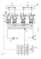
- FIG. 2 illustrates a schematic configuration of the circuit board testing apparatus 1 .
- the circuit board testing apparatus 1 includes a power supply part 2 , a detection part 3 , a calculation part 4 , a determination part 5 , a selection part 6 , a memory part 10 , a display part 11 , and the like.
- the circuit board testing apparatus 1 is provided with a jig (not illustrated) for electrically connecting between a wire T on a circuit board CB and the circuit board testing apparatus 1 .
- the jig has a contact CP coming into contact with a predetermined test point on the wire T.
- FIG. 2 illustrates the circuit board testing apparatus 1 prepared to conduct a continuity test on the circuit board CB, and also illustrates two wires T 1 and T 2 on the circuit board CB.
- the wires T 1 and T 2 are subjected to a continuity test based on a two-terminal measurement method.
- two contacts CP are brought into electrical contact with a first end of the wire T
- two contacts CP are brought into electrical contact with a second end of the wire T.
- the four-terminal measurement method is implemented using the two contacts CP connected to each of the first and second ends of the wire T, as a pair of contacts, i.e., a current feeding contact and a voltage measuring contact.
- the power supply part 2 supplies power for testing the continuity state of the wire T on the circuit board CB.
- the power supply part 2 is capable of feeding current having at least two values, i.e., a first current value and a second current value.
- the power supply part 2 may be, for example, a constant current source. In this case, the power supply part 2 transmits a value of current to be fed to the wire T, as current value information, to the calculation part 4 and the like.
- the detection part 3 detects voltage at the wire T being tested, in the state that the power supply part 2 supplies power to the wire T.
- the calculation part 4 calculates a resistance value of the wire T on the basis of the detected voltage at the wire T, as will be described later.
- the detection part 3 may be a voltmeter.
- the power supply part 2 , the detection part 3 , and a current detection part 12 are connected to the calculation part 4 , the memory part 10 , and the like to transmit, as information, current feeding conditions (current value, voltage value) for conduct of the continuity test, and the detected current value and voltage value.
- the detection part 3 successively measures a voltage value of the wire T to which power is supplied.
- the detection part 3 transmits the voltage value as measurement information (voltage value information) to the memory part 10 and the like, as described above.
- the calculation part 4 calculates the resistance value of the wire T being tested, on the basis of the voltage value information detected by the detection part 3 .
- the calculation part 4 calculates the resistance value on the basis of the current value information from the power supply part 2 and the voltage value information from the detection part 3 .
- the calculation part 4 may calculate the resistance value by performing arithmetic processing using, for example, Ohm's law.
- the calculation part 4 transmits the calculation result (resistance value information) to the determination part 5 and the memory part 10 .
- the determination part 5 determines whether or not the continuity state of the wire T being tested is favorable, on the basis of the resistance value calculated by the calculation part 4 .
- the determination part 5 may make the determination based on the resistance value information by defining a range of resistance that identifies a favorable continuity state. When the resistance value falls within the defined range, the determination part 5 may determine that the continuity state is favorable.
- the determination part 5 transmits the determination result (determination information) to the memory part 10 and the display part 11 .
- the determination part 5 detects whether maintenance is needed on the contact CP, on the basis of a change of the voltage value information detected by the detection part 3 .
- the determination part 5 successively monitors the voltage value information of the wire T in the continuity test.
- the determination part 5 is capable of obtaining maintenance information (replacement information) on the contact CP from the change of the voltage value information.
- the determination part 5 may obtain the maintenance information as follows.
- the determination part 5 obtains information that the contact CP should be replaced, when the voltage changes in a predetermined way when power is supplied.
- the determination part 5 obtains the replacement information based on whether or not there is a successive rise in voltage applied to the wire T being tested. More specifically, the determination part 5 successively stores therein the voltage value information detected by the detection part 3 , thereby detecting successive changes in the voltage over time.
- the determination part 5 determines when it is time to replace the contact CP, on the basis of the successive change of the voltage value information. Therefore, the determination part 5 is capable of determining whether or not to replace the contact CP, in accordance with the successive change of the voltage value information.
- FIG. 3A is a graph illustrating the change of the voltage value information in the case where the contact CP is normal.
- the voltage rises with a fixed gradient except for the voltage immediately after the start of power supply (around a point in time t 1 ), and the voltage immediately before a steady voltage value is reached for conducting the continuity test (around a point in time t 2 ).
- the contact CP is abnormal, the voltage does not rise at a substantially fixed rate or gradient. As illustrated in FIG.
- the voltage may temporarily drop (a temporal voltage drop at a point in time t 4 ) or otherwise deviate from a fixed rate of rise.
- the voltage does not rise with a fixed gradient, there is a high possibility that the contact CP is abnormal. Identifying such phenomenon allows management of when it is time to replace the contact CP.
- the determination part 5 determines that the contact CP is normal (i.e., the contact CP does not need to be replaced) in the case where the voltage value increases at a constant rate or gradient. On the other hand, the determination part 5 determines that the contact CP is abnormal (i.e., the contact CP needs to be replaced) in the case where the voltage value does not increase at a constant rate or gradient.
- the determination part 5 makes such a determination by monitoring the change of the voltage value during a period of time from the start of power supply for the continuity test to the start of measurement for the continuity test.
- the determination part 5 may determine that the contact CP needs to be replaced, upon detection of a negative gradient, i.e., a decrease of the voltage value.
- the determination part 5 may make such a determination by monitoring the voltage value for a predetermined period of time when the power is supplied, and identifying how the voltage value increases in that period of time. When the voltage value does not increase at a constant rate (gradient) in the predetermined period of time, the determination part 5 determines that the contact CP needs to be replaced.
- gradient constant rate
- the display part 11 displays the contact CP and a message prompting a user to replace the contact CP.
- the determination part 5 makes the foregoing determination by monitoring the voltage value information during the period of time from the start of the power supply to the conduct of the continuity test. In order to more accurately detect the time to replace the contact CP, the determination part 5 may monitor the voltage value in a multilevel manner.
- the determination part 5 may monitor the voltage value in a multilevel manner based on a first voltage value to be set for conducting the continuity test and a second voltage value to be set for determining the time to replace the contact CP.
- the first voltage value is set to be smaller than the second voltage value.
- the voltage value is increased to the second voltage value.
- the determination part 5 monitors the voltage value so as to detect the replacement information during the period of time from the first voltage value to the second voltage value.
- the determination part 5 When the determination part 5 detects the need for a replacement (a predetermined change of the voltage value) during the period of time from the first voltage value to the second voltage value, then the determination part 5 issues a replacement information request on the contact CP. As described above, the determination part 5 utilizes, as preliminary replacement information, the replacement information issued by the point in time when the voltage value reaches the first voltage value. When the preliminary replacement information is detected, the voltage value is increased to the second voltage value. Thus, the determination part 5 is capable of determining whether or not the contact CP needs to be replaced, on the basis of the change of the voltage value in this interval.
- V 1 represents the first voltage value
- V 2 represents the second voltage value.
- the determination part 5 monitors whether or not the voltage drops at the first voltage value V 1 and whether or not the voltage drops at the second voltage value V 2 .
- the determination part 5 determines that the contact CP does not need to be replaced, and the continuity test is conducted. In this case, the continuity test may be conducted at the second voltage value.
- the determination part 5 detects a voltage drop p 2 in the period of time from the first voltage value V 1 to the second voltage value V 2 , then the determination part 5 determines that the contact CP is abnormal, and the contact CP electrically connected to the target object is replaced with a new one.
- the determination part 5 stores therein the point in time and the voltage value upon detection of the voltage drop p 2 . Particularly, storing the voltage value upon detection of the voltage drop p 2 allows more accurate detection of a time to replace the contact CP.
- the determination part 5 may determine whether or not the contact CP needs to be replaced, again, on the basis of the voltage value upon detection of the replacement information based upon a change in gradient in the interval. Specifically, the determination part 5 defines, as a detected voltage value, the voltage value upon detection of the replacement information in the interval from the first voltage value V 1 to the second voltage value V 2 . Then the determination part 5 may estimate a necessity to replace the contact CP and a time to replace the contact CP, on the basis of the detected voltage value.
- the determination part 5 may determine that the contact CP does not need to be replaced.
- the determination part 5 may determine that the contact CP needs to be replaced.
- the determination part 5 may determine that the contact CP does not need to be replaced and therefore can be continuously used.
- the determination part 5 may determine that the contact CP needs to be replaced.
- a third voltage value may be set in addition to the second voltage value (first voltage value ⁇ third voltage value ⁇ second voltage value). The determination part 5 may determine that the contact CP needs to be replaced, when the voltage value exceeds the third voltage value upon detection of the replacement information.
- the user may appropriately set the specific first and second voltage values depending on a target object.
- the first voltage value may be set at 150 V
- the second voltage value may be set at 250 V.
- the first voltage value is a voltage limit value upon conduct of the continuity test on the target object.
- the second voltage value is a voltage value for detection of an abnormal contact CP. Therefore, these voltage values are appropriately set depending on conditions of a test.
- the determination part 5 issues replacement information when the detected voltage value does not increase at a constant rate, thereby prompting the user to replace the contact CP.
- the replacement information from the determination part 5 may be directly processed as a time to replace a contact CP, as described above. Alternatively, a time to replace a contact CP may be determined upon reception of replacement information again with the preceding replacement information set as a trigger.
- the function of the determination part 5 is set in advance prior to conducting the continuity test on a target object.
- the selection part 6 selects and specifies a wire T to be tested from the plurality of wires T on the circuit board CB.
- the wires T are sequentially selected as a target object to be subjected to the continuity test in such a manner that the selection part 6 specifies the wire T as described above.
- the selection part 6 may select the wire T in accordance with a preset order of wires T to be tested, and such order may be stored in the memory part 10 .
- the selection part 6 may select the wire T as described above, but not limited thereto as long as the wires T to be tested can be selected sequentially.
- the selection part 6 selects the wire T to be tested, using a switch part 7 including switching elements SW.
- the selection part 6 is capable of selecting the wire T by closing and opening the switching element SW of the switch part 7 .
- the specific method of closing and opening the switching element SW is described below.
- Current feeding terminals 8 are connected to the wire T via the contacts CP to feed a current to the wire T.
- Each of the current feeding terminals 8 includes an upstream current feeding terminal 81 and a downstream current feeding terminal 82 .
- the upstream current feeding terminal 81 connects an upstream side (positive electrode side) of the power supply part 2 to the wire T.
- the downstream current feeding terminal 82 connects a downstream side (negative electrode side) of the power supply part 2 or the current detection part 12 to the wire T.
- the upstream current feeding terminal 81 and downstream current feeding terminal 82 of the current feeding terminal 8 are disposed to correspond to a test point on the wire T.
- the upstream current feeding terminal 81 and the downstream current feeding terminal 82 are connected to the switching elements SW of the switch part 7 , respectively.
- the upstream current feeding terminal 81 and the downstream current feeding terminal 82 are connected to and disconnected from the switching elements SW of the switch part 7 in such a manner that the switch part 7 closes and opens the respective switching elements SW.
- the current feeding terminal 8 may be provided with a resistor for protection from electrostatic discharge.
- Voltage detecting terminals 9 are connected to the wire T via the contacts CP to detect voltage at the wire T.
- Each of the voltage detecting terminals 9 includes an upstream voltage detecting terminal 91 and a downstream voltage detecting terminal 92 .
- the upstream voltage detecting terminal 91 connects an upstream side (positive electrode side) of the detection part 3 to the wire T.
- the downstream voltage detecting terminal 92 connects a downstream side (negative electrode side) of the detection part 3 to the wire T.
- the upstream voltage detecting terminal 91 and downstream voltage detecting terminal 92 of the voltage detecting terminal 9 are disposed to correspond to the test point on the wire T.
- the upstream voltage detecting terminal 91 and the downstream voltage detecting terminal 92 are connected to the switching elements SW of the switch part 7 , respectively.
- the upstream voltage detecting terminal 91 and the downstream voltage detecting terminal 92 are connected to and disconnected from the switching elements SW of the switch part 7 in such a manner that the switch part 7 closes and opens the switching elements SW.
- the four terminals of the current feeding terminal 8 and voltage detecting terminal 9 are connected to one contact CP which is in electrical contact with the test point on the wire T.
- the four terminals of the current feeding terminal 8 and voltage detecting terminal 9 are also connected to the four switching elements SW for performing the ON/OFF control on the respective terminals.
- the switch part 7 includes the plurality of switching elements SW electrically connected to the corresponding terminals.
- the switch part 7 closes and opens each switching element SW on the basis of an operation signal from the selection part 6 , as will be described later.
- FIG. 5 illustrates a case where a wire T 1 is a target object to be subjected to the continuity test.
- the switching element SW 1 is closed to electrically connect the upstream current feeding terminal 81 , which is connected to a first end P 1 a of the wire T 1 , to the upstream side of the power supply part 2 .
- the switching element SW 2 is closed to electrically connect the upstream voltage detecting terminal 91 , which is connected to the first end P 1 a of the wire T 1 , to the upstream side of the detection part 3 .
- the switching element SW 4 is closed to electrically connect the downstream current feeding terminal 82 , which is connected to a second end P 1 b of the wire T 1 , to the downstream side of the power supply part 2 (or the current detection part 12 ).
- the switching element SW 3 is closed to electrically connect the downstream voltage detecting terminal 92 , which is connected to the second end P 1 b of the wire T 1 , to the downstream side of the detection part 3 .
- the selection part 6 is capable of selecting the wire T to be tested, by closing and opening the switching element SW of the switch part 7 .
- the circuit board testing apparatus 1 may include the current detection part 12 .
- the current detection part 12 is capable of detecting current flowing through a wire T being tested.
- the current detection part 12 is capable of detecting current fed from the power supply part 2 for the purpose of a check.
- the memory part 10 stores therein information for conducting the continuity test on a wire T on the circuit board CB.
- the continuity test is conducted on all the wires T on the basis of the information stored in the memory part 10 .
- the memory part 10 may also store therein results of processing by the respective parts.
- the memory part 10 successively stores therein the detection results by the detection part 3 such that the determination part 5 detects the change in voltage value.
- the determination part 5 detects the change in voltage value on the basis of the voltage value information stored in the memory part 10 .
- the display part 11 displays, for example, the information on the current fed from the power supply part 2 , the information on the detection by the detection part 3 , and the information on the determination by the determination part 5 .
- the information displayed on the display part 11 allows the user of the circuit board testing apparatus 1 to understand the state and result of the continuity test.
- a contact CP is in contact with a target object T.
- the number of contacts CP coming into contact with the target object T is not limited to two as illustrated in FIG. 1 .
- determination as to whether or not the contact CP is abnormal may be made on each of the two contacts CP or may be made on the contact CP electrically connected to the positive electrode of the power supply part 2 .
- the other contact CP can be subjected to the same test by changing the polarity.
- the foregoing description concerns the configuration of the circuit board testing apparatus 1 according to one or more embodiments of the disclosure.
- one of the wires T on the circuit board CB is selected as a target object, and then is subjected to the continuity test.
- the wire T is determined to be favorable, the next wire T is selected as a target object, and then is subjected to the continuity test.
- the selecting method is not described, but the continuity test to be conducted on a wire T selected as a target object is specifically described.
- the first voltage value is set at, for example, 250 V.
- the continuity test is conducted on the wire T to be tested.
- FIG. 5 illustrates the continuity test conducted on the wire T 1 selected as a target object.
- the selection part 6 transmits a signal to close or open the switching element SW of the switch part 7 in accordance with the order of wires T to be tested.
- the continuity test is conducted on the wire T 1 .
- the detection part 3 detects a value of voltage applied to the wire T 1 .
- the detection part 3 monitors the voltage value of the wire T 1 during the period of time from the start of voltage application to the wire T 1 to the conduct of the continuity test.
- the determination part 5 monitors the change of the voltage value detected by the detection part 3 , during the period of time from the start of voltage application to the conduct of the continuity test. When the voltage value increases at a constant rate, the determination part 5 issues no replacement information. In other words, the determination part 5 determines that the contact CP is normal. Therefore, the contact CP continues to be used.
- the determination part 5 issues the replacement information. In other words, the determination part 5 determines that the contact CP is abnormal. Therefore, the contact CP is replaced with a new one after the continuity test.
- the method according to one or more embodiments of the disclosure is capable of determining a time to replace a contact CP before a continuity test cannot be conducted on a target object. Therefore, the method according to one or more embodiments of the disclosure is capable of reducing a cause of a contact failure of a contact with a target object, and is capable of preventing reduction in productivity due to the contact failure.
- the first voltage value is set as a voltage limit value for conducting the continuity test on a target object
- the second voltage value is set as a voltage value for testing as to whether a contact is abnormal.
- the first voltage value is set at 150 V
- the second voltage value is set at 250 V.
- the power supply part 2 supplies power for conducting the continuity test on the target object.
- the power supplied from the power supply part 2 has the first voltage value as the voltage limit value.
- the detection part 3 continuously detects the voltage value of the target object, and transmits the detected voltage value during the period of time from the start of voltage application to the finish of the continuity test.
- the determination part 5 detects a change of the successively stored voltage values. With regard to the successive change, the determination part 5 monitors whether the voltage value increases at a constant rate. When the voltage value increases at a constant rate, the determination part 5 determines that the contact CP is normal. Thus, the continuity test may be conducted.
- the determination part 5 determines that the voltage value does not increase at a constant rate (for example, when the determination part 5 detects a voltage drop). Then the determination part 5 monitors the change in voltage value from the first voltage value to the second voltage value. The determination part 5 monitors whether the voltage value increases from the first voltage value to the second voltage value at a constant rate. When it is determined that the voltage value increases at a constant rate, the continuity test is conducted. On the other hand, when the voltage value does not increase at a constant rate because of, for example, a voltage drop, the determination part 5 determines that the contact CP needs to be replaced, and then transmits replacement information indicating that the contact CP should be replaced.
Applications Claiming Priority (2)
| Application Number | Priority Date | Filing Date | Title |
|---|---|---|---|
| JP2013226365A JP6252106B2 (ja) | 2013-10-31 | 2013-10-31 | 接触子のメンテナンス方法及び検査装置 |
| JP2013-226365 | 2013-10-31 |
Publications (2)
| Publication Number | Publication Date |
|---|---|
| US20150115974A1 US20150115974A1 (en) | 2015-04-30 |
| US9678134B2 true US9678134B2 (en) | 2017-06-13 |
Family
ID=52994699
Family Applications (1)
| Application Number | Title | Priority Date | Filing Date |
|---|---|---|---|
| US14/528,115 Active 2035-04-02 US9678134B2 (en) | 2013-10-31 | 2014-10-30 | Method for determining maintenance time for contacts, and testing apparatus |
Country Status (5)
| Country | Link |
|---|---|
| US (1) | US9678134B2 (zh) |
| JP (1) | JP6252106B2 (zh) |
| KR (1) | KR102216324B1 (zh) |
| CN (1) | CN104597364B (zh) |
| TW (1) | TWI664427B (zh) |
Cited By (1)
| Publication number | Priority date | Publication date | Assignee | Title |
|---|---|---|---|---|
| US10215790B2 (en) * | 2014-11-04 | 2019-02-26 | Continental Automotive France | Method for diagnosing an earth fault of a start/stop unit of a motor vehicle |
Families Citing this family (7)
| Publication number | Priority date | Publication date | Assignee | Title |
|---|---|---|---|---|
| US9063191B2 (en) * | 2012-02-24 | 2015-06-23 | Power Probe, Inc. | Electrical test device and method |
| JP6961385B2 (ja) * | 2017-05-08 | 2021-11-05 | 日置電機株式会社 | 検査装置 |
| JP6957195B2 (ja) * | 2017-05-16 | 2021-11-02 | 日置電機株式会社 | 測定装置 |
| CN108490242B (zh) * | 2018-04-02 | 2020-03-27 | 国网江苏省电力有限公司徐州供电分公司 | 一种新型验电装置 |
| TW202115413A (zh) * | 2019-09-30 | 2021-04-16 | 日商愛德萬測試股份有限公司 | 維護裝置、維護方法及記錄有維護程式之記錄媒體 |
| US11860189B2 (en) | 2019-12-12 | 2024-01-02 | Innova Electronics Corporation | Rotational electrical probe |
| CN113159630B (zh) * | 2021-05-13 | 2021-11-23 | 北京三维天地科技股份有限公司 | 一种用于实验室信息管理系统中维护计算公式的方法 |
Citations (10)
| Publication number | Priority date | Publication date | Assignee | Title |
|---|---|---|---|---|
| US4342957A (en) * | 1980-03-28 | 1982-08-03 | Honeywell Information Systems Inc. | Automatic test equipment test probe contact isolation detection apparatus and method |
| JPH07161783A (ja) | 1993-12-13 | 1995-06-23 | Nec Corp | 半導体測定装置及びその測定状態設定方法 |
| US5677839A (en) * | 1994-12-02 | 1997-10-14 | Mitsubishi Denki Kabushiki Kaisha | On-vehicle electronic control device and a method of detecting a failure thereof |
| US20060292710A1 (en) * | 2005-06-22 | 2006-12-28 | Waukesha Electric Systems, Incorporated | Sensor and method for detecting electric contact degradation |
| US20080024139A1 (en) * | 2004-07-23 | 2008-01-31 | Valeo Electronique Et Systemes De Liaison | Device and a Method for Testing At Least One Conductive Joint Forming an Electrical Connection Between an Electrical Component and a Printed Circuit |
| US20090308734A1 (en) * | 2008-06-17 | 2009-12-17 | Schneider Automation Inc. | Apparatus and Method for Wafer Level Arc Detection |
| US20120025844A1 (en) * | 2009-06-12 | 2012-02-02 | Nissan Motor Co., Ltd | Connection diagnostic apparatus for ground fault detector |
| US20130221973A1 (en) * | 2012-02-24 | 2013-08-29 | Power Probe, Inc. | Electrical test device and method |
| US20130293188A1 (en) * | 2011-01-18 | 2013-11-07 | Nissan Motor Co., Ltd. | Charging apparatus and method for determining conduction state |
| US20140306732A1 (en) * | 2013-04-14 | 2014-10-16 | Infineon Technologies Austria Ag | Detection of defective electrical connections |
Family Cites Families (8)
| Publication number | Priority date | Publication date | Assignee | Title |
|---|---|---|---|---|
| JP3239544B2 (ja) * | 1993-07-28 | 2001-12-17 | 株式会社豊田自動織機 | コンタクタの動作状態判定装置 |
| JP3369536B2 (ja) * | 2000-06-02 | 2003-01-20 | 弘伸 中野 | 接続不良検出装置 |
| JP3546046B2 (ja) * | 2001-09-26 | 2004-07-21 | 日本電産リード株式会社 | 回路基板の絶縁検査装置及び絶縁検査方法 |
| GB2394780B (en) * | 2002-10-29 | 2006-06-14 | Ifr Ltd | A method of and apparatus for testing for integrated circuit contact defects |
| JP3953087B2 (ja) * | 2005-10-18 | 2007-08-01 | 日本電産リード株式会社 | 絶縁検査装置及び絶縁検査方法 |
| JP5428748B2 (ja) * | 2009-10-21 | 2014-02-26 | 日本電産リード株式会社 | 検査用治具のメンテナンス方法及び基板検査装置 |
| JP5541720B2 (ja) * | 2010-08-30 | 2014-07-09 | 日置電機株式会社 | 検査装置 |
| CN105452886B (zh) * | 2013-04-11 | 2018-02-13 | 瑞萨电子株式会社 | 半导体器件的制造方法 |
-
2013
- 2013-10-31 JP JP2013226365A patent/JP6252106B2/ja active Active
-
2014
- 2014-10-16 CN CN201410548812.XA patent/CN104597364B/zh active Active
- 2014-10-20 KR KR1020140141429A patent/KR102216324B1/ko active IP Right Grant
- 2014-10-23 TW TW103136658A patent/TWI664427B/zh active
- 2014-10-30 US US14/528,115 patent/US9678134B2/en active Active
Patent Citations (10)
| Publication number | Priority date | Publication date | Assignee | Title |
|---|---|---|---|---|
| US4342957A (en) * | 1980-03-28 | 1982-08-03 | Honeywell Information Systems Inc. | Automatic test equipment test probe contact isolation detection apparatus and method |
| JPH07161783A (ja) | 1993-12-13 | 1995-06-23 | Nec Corp | 半導体測定装置及びその測定状態設定方法 |
| US5677839A (en) * | 1994-12-02 | 1997-10-14 | Mitsubishi Denki Kabushiki Kaisha | On-vehicle electronic control device and a method of detecting a failure thereof |
| US20080024139A1 (en) * | 2004-07-23 | 2008-01-31 | Valeo Electronique Et Systemes De Liaison | Device and a Method for Testing At Least One Conductive Joint Forming an Electrical Connection Between an Electrical Component and a Printed Circuit |
| US20060292710A1 (en) * | 2005-06-22 | 2006-12-28 | Waukesha Electric Systems, Incorporated | Sensor and method for detecting electric contact degradation |
| US20090308734A1 (en) * | 2008-06-17 | 2009-12-17 | Schneider Automation Inc. | Apparatus and Method for Wafer Level Arc Detection |
| US20120025844A1 (en) * | 2009-06-12 | 2012-02-02 | Nissan Motor Co., Ltd | Connection diagnostic apparatus for ground fault detector |
| US20130293188A1 (en) * | 2011-01-18 | 2013-11-07 | Nissan Motor Co., Ltd. | Charging apparatus and method for determining conduction state |
| US20130221973A1 (en) * | 2012-02-24 | 2013-08-29 | Power Probe, Inc. | Electrical test device and method |
| US20140306732A1 (en) * | 2013-04-14 | 2014-10-16 | Infineon Technologies Austria Ag | Detection of defective electrical connections |
Cited By (1)
| Publication number | Priority date | Publication date | Assignee | Title |
|---|---|---|---|---|
| US10215790B2 (en) * | 2014-11-04 | 2019-02-26 | Continental Automotive France | Method for diagnosing an earth fault of a start/stop unit of a motor vehicle |
Also Published As
| Publication number | Publication date |
|---|---|
| TW201530146A (zh) | 2015-08-01 |
| KR20150050377A (ko) | 2015-05-08 |
| CN104597364B (zh) | 2019-01-11 |
| CN104597364A (zh) | 2015-05-06 |
| US20150115974A1 (en) | 2015-04-30 |
| JP2015087272A (ja) | 2015-05-07 |
| TWI664427B (zh) | 2019-07-01 |
| KR102216324B1 (ko) | 2021-02-17 |
| JP6252106B2 (ja) | 2017-12-27 |
Similar Documents
| Publication | Publication Date | Title |
|---|---|---|
| US9678134B2 (en) | Method for determining maintenance time for contacts, and testing apparatus | |
| US10175284B2 (en) | Circuit board testing apparatus and circuit board testing method | |
| US10228411B2 (en) | Testing apparatus | |
| KR102277218B1 (ko) | 웨이퍼 레벨에서의 정확하고 저비용의 전압 측정을 위한 전류 조정 | |
| US8427182B2 (en) | Test apparatus and power supply apparatus | |
| WO2008041678A1 (fr) | Appareil de test de carte et procédé de test de carte | |
| US20150067378A1 (en) | Measuring apparatus, measuring method, and measuring system | |
| TWI498571B (zh) | 絕緣檢測裝置及絕緣檢測方法 | |
| TW201500743A (zh) | 基板檢查裝置 | |
| US10197616B2 (en) | Insulation inspection method and insulation inspection apparatus | |
| JP6219073B2 (ja) | 絶縁検査装置 | |
| TW201508288A (zh) | 檢測裝置 | |
| US20110279124A1 (en) | Float current monitor | |
| TWI621863B (zh) | 基板檢查裝置及基板檢查方法 | |
| JP2000230960A (ja) | コネクタ接触状態検査装置 | |
| TW201428305A (zh) | 檢測夾具之檢測方法 | |
| JP6219074B2 (ja) | 絶縁検査装置 | |
| KR20140085066A (ko) | 기판 검사 장치 및 기판 검사 방법 |
Legal Events
| Date | Code | Title | Description |
|---|---|---|---|
| AS | Assignment |
Owner name: NIDEC-READ CORPORATION, JAPAN Free format text: ASSIGNMENT OF ASSIGNORS INTEREST;ASSIGNOR:YAMASHITA, MUNEHIRO;REEL/FRAME:034387/0576 Effective date: 20141114 |
|
| STCF | Information on status: patent grant |
Free format text: PATENTED CASE |
|
| MAFP | Maintenance fee payment |
Free format text: PAYMENT OF MAINTENANCE FEE, 4TH YEAR, LARGE ENTITY (ORIGINAL EVENT CODE: M1551); ENTITY STATUS OF PATENT OWNER: LARGE ENTITY Year of fee payment: 4 |