US9525426B2 - Cross-coupled input voltage sampling and driver amplifier flicker noise cancellation in a switched capacitor analog-to-digital converter - Google Patents
Cross-coupled input voltage sampling and driver amplifier flicker noise cancellation in a switched capacitor analog-to-digital converter Download PDFInfo
- Publication number
- US9525426B2 US9525426B2 US14/615,001 US201514615001A US9525426B2 US 9525426 B2 US9525426 B2 US 9525426B2 US 201514615001 A US201514615001 A US 201514615001A US 9525426 B2 US9525426 B2 US 9525426B2
- Authority
- US
- United States
- Prior art keywords
- switch
- stage
- phase
- input
- signal
- Prior art date
- Legal status (The legal status is an assumption and is not a legal conclusion. Google has not performed a legal analysis and makes no representation as to the accuracy of the status listed.)
- Active
Links
Images


Classifications
-
- H—ELECTRICITY
- H03—ELECTRONIC CIRCUITRY
- H03F—AMPLIFIERS
- H03F1/00—Details of amplifiers with only discharge tubes, only semiconductor devices or only unspecified devices as amplifying elements
- H03F1/26—Modifications of amplifiers to reduce influence of noise generated by amplifying elements
-
- H—ELECTRICITY
- H03—ELECTRONIC CIRCUITRY
- H03M—CODING; DECODING; CODE CONVERSION IN GENERAL
- H03M1/00—Analogue/digital conversion; Digital/analogue conversion
- H03M1/06—Continuously compensating for, or preventing, undesired influence of physical parameters
- H03M1/08—Continuously compensating for, or preventing, undesired influence of physical parameters of noise
- H03M1/0836—Continuously compensating for, or preventing, undesired influence of physical parameters of noise of phase error, e.g. jitter
-
- H—ELECTRICITY
- H03—ELECTRONIC CIRCUITRY
- H03M—CODING; DECODING; CODE CONVERSION IN GENERAL
- H03M1/00—Analogue/digital conversion; Digital/analogue conversion
- H03M1/06—Continuously compensating for, or preventing, undesired influence of physical parameters
- H03M1/08—Continuously compensating for, or preventing, undesired influence of physical parameters of noise
-
- H—ELECTRICITY
- H03—ELECTRONIC CIRCUITRY
- H03F—AMPLIFIERS
- H03F3/00—Amplifiers with only discharge tubes or only semiconductor devices as amplifying elements
- H03F3/45—Differential amplifiers
- H03F3/45071—Differential amplifiers with semiconductor devices only
- H03F3/45076—Differential amplifiers with semiconductor devices only characterised by the way of implementation of the active amplifying circuit in the differential amplifier
- H03F3/45475—Differential amplifiers with semiconductor devices only characterised by the way of implementation of the active amplifying circuit in the differential amplifier using IC blocks as the active amplifying circuit
-
- H—ELECTRICITY
- H03—ELECTRONIC CIRCUITRY
- H03K—PULSE TECHNIQUE
- H03K17/00—Electronic switching or gating, i.e. not by contact-making and –breaking
- H03K17/10—Modifications for increasing the maximum permissible switched voltage
-
- H—ELECTRICITY
- H03—ELECTRONIC CIRCUITRY
- H03M—CODING; DECODING; CODE CONVERSION IN GENERAL
- H03M1/00—Analogue/digital conversion; Digital/analogue conversion
- H03M1/06—Continuously compensating for, or preventing, undesired influence of physical parameters
- H03M1/08—Continuously compensating for, or preventing, undesired influence of physical parameters of noise
- H03M1/089—Continuously compensating for, or preventing, undesired influence of physical parameters of noise of temperature variations
-
- H—ELECTRICITY
- H03—ELECTRONIC CIRCUITRY
- H03M—CODING; DECODING; CODE CONVERSION IN GENERAL
- H03M1/00—Analogue/digital conversion; Digital/analogue conversion
- H03M1/12—Analogue/digital converters
- H03M1/124—Sampling or signal conditioning arrangements specially adapted for A/D converters
-
- H—ELECTRICITY
- H03—ELECTRONIC CIRCUITRY
- H03M—CODING; DECODING; CODE CONVERSION IN GENERAL
- H03M1/00—Analogue/digital conversion; Digital/analogue conversion
- H03M1/12—Analogue/digital converters
- H03M1/124—Sampling or signal conditioning arrangements specially adapted for A/D converters
- H03M1/1245—Details of sampling arrangements or methods
-
- H—ELECTRICITY
- H03—ELECTRONIC CIRCUITRY
- H03M—CODING; DECODING; CODE CONVERSION IN GENERAL
- H03M3/00—Conversion of analogue values to or from differential modulation
- H03M3/30—Delta-sigma modulation
- H03M3/322—Continuously compensating for, or preventing, undesired influence of physical parameters
- H03M3/368—Continuously compensating for, or preventing, undesired influence of physical parameters of noise other than the quantisation noise already being shaped inherently by delta-sigma modulators
- H03M3/37—Compensation or reduction of delay or phase error
- H03M3/372—Jitter reduction
-
- H—ELECTRICITY
- H03—ELECTRONIC CIRCUITRY
- H03M—CODING; DECODING; CODE CONVERSION IN GENERAL
- H03M3/00—Conversion of analogue values to or from differential modulation
- H03M3/30—Delta-sigma modulation
- H03M3/458—Analogue/digital converters using delta-sigma modulation as an intermediate step
-
- H—ELECTRICITY
- H03—ELECTRONIC CIRCUITRY
- H03F—AMPLIFIERS
- H03F2203/00—Indexing scheme relating to amplifiers with only discharge tubes or only semiconductor devices as amplifying elements covered by H03F3/00
- H03F2203/45—Indexing scheme relating to differential amplifiers
- H03F2203/45614—Indexing scheme relating to differential amplifiers the IC comprising two cross coupled switches
Definitions
- the present disclosure relates to switched capacitor systems and, in particular, to cross-coupled input voltage sampling and driver amplifier flicker noise cancellation in switched capacitor analog to digital converter (ADC).
- ADC switched capacitor analog to digital converter
- ⁇ ADCs comprise a switched capacitor integrator as its first stage in order to sample the input signal.
- noise such as thermal noise.
- this thermal noise e.g., thermal KT/C noise
- ⁇ ADCs include a driver amplifier, which generates flicker noise associated with it that further degrades the performance of the ⁇ ADCs. Therefore, it is desirable for a switched capacitor system to operate with low thermal noise and low flicker noise.
- a switched capacitor system comprises a switching stage comprising a plurality of switches configured to receive a differential signal at an input of the switching stage and provide a non-inverted version of the differential signal at an output of the switching stage during a first phase of operation and an inverted version of the differential signal at the output of the switching stage during a second phase of operation.
- the switched capacitor system further comprises a driver stage comprising an amplifier, located downstream of the switching stage, configured to receive the non-inverted version of the differential signal at an input of the driver stage during the first phase of operation and the inverted version of the differential signal at the input of the driver stage during the second phase of operation.
- a sampling capacitor stage is configured to sample an output of the driver stage during the first phase of operation and the second phase of operation and provide a cancellation of a flicker noise and an offset of the driver stage during the second phase of operation.
- the switched capacitor system comprises a switching controller configured to control a cross-coupled configuration of the plurality of switches and increase a signal-to-noise ratio of the sampling capacitor stage by approximately doubling a transferred charge and corresponding signal swing across the sampling capacitor stage.
- an analog to digital converter system comprises a switching component configured to receive a differential signal at a first signal branch and a second signal branch, comprising a first set of switches configured to provide a non-inverted version of the differential signal at an output of the switching component during a first phase of operation, and a second set of switches configured to provide an inverted version of the differential signal at the output of the switching component during a second phase of operation.
- the analog to digital converter system further comprises a driver component configured to generate a drive signal to the first signal branch and the second signal branch based on the non-inverted version of the differential signal during the first phase of operation and based on the inverted version of the differential signal during the second phase of operation.
- a sampling component is configured to sample the drive signal of the driver component, generate a charge transfer to a first sampling capacitor and a second sampling capacitor during the first phase of operation and the second phase of operation, and generate a cancellation of a flicker noise and an offset of the driver component during the second phase of operation.
- the analog to digital converter system comprises a switching control component configured control a cross-coupled configuration of the first set of switches and the second set of switches and increase a signal-to-noise ratio of the sampling component by approximately doubling a charge transfer and corresponding signal swing across the first sampling capacitor and the second sampling capacitor.
- the method further comprises sampling the second portion of the analog differential signal at a second sampling capacitance in the first phase of operation, and generating a first charge transfer to the second sampling capacitance, sampling the first portion of the analog differential signal, comprising an inverted version of the second portion of the analog differential signal at the second sampling capacitance in the second phase of operation, and generating a second charge transfer to the second sampling capacitance and providing, via a second amplifier, the second portion and the first portion of the analog differential signal prior to the first charge transfer and the second charge transfer to the second sampling capacitance.
- FIG. 1 illustrates a block diagram of a ADC with a sampling circuit and an integrator according to one embodiment of the disclosure
- FIG. 2 illustrates a schematic diagram of a sampling circuit of an integrator, according to another embodiment of the disclosure
- FIG. 3 illustrates another schematic diagram of a sampling circuit of an integrator with a fully differential buffer amplifier, according to another embodiment of the disclosure
- FIG. 4 a illustrates another schematic diagram of a fully differential switched capacitor integrator with a sampling circuit, according to another embodiment of the present disclosure
- FIG. 4 b illustrates an example of a two-phase non-overlapping clock defined by four clock waveforms ⁇ 1 , ⁇ 1 d , ⁇ 2 and ⁇ 2 d;
- FIG. 4 c illustrates an example of amplitudes of a differential input signal during clock waveforms ⁇ 1 and ⁇ 2 ;
- FIG. 4 d illustrates an example of amplitudes of a differential output of the buffer amplifier during clock waveforms ⁇ 1 and ⁇ 2 ;
- FIG. 4 e illustrates an example of amplitudes of the differential buffer output low-frequency noise or offset during ⁇ 1 and ⁇ 2 ;
- FIG. 5 illustrates another schematic diagram a fully differential switched capacitor integrator with a fully differential buffer amplifier, according to another embodiment of the present disclosure
- FIG. 6 illustrates another schematic diagram of a fully differential switched capacitor integrator with buffer amplifiers implemented as source followers, according to the present disclosure.
- FIG. 7 illustrates a flowchart of a method of sampling a differential signal, according to an embodiment of the present disclosure
- a component can be a processor, a process running on a processor, a controller, an object, an executable, a program, a storage device, and/or a computer with a processing device.
- an application running on a server and the server can also be a component.
- these components can execute from various computer readable storage media having various data structures stored thereon such as with a module, for example.
- the components can communicate via local and/or remote processes such as in accordance with a signal having one or more data packets (e.g., data from one component interacting with another component in a local system, distributed system, and/or across a network, such as, the Internet, a local area network, a wide area network, or similar network with other systems via the signal).
- a signal having one or more data packets (e.g., data from one component interacting with another component in a local system, distributed system, and/or across a network, such as, the Internet, a local area network, a wide area network, or similar network with other systems via the signal).
- a component can be an apparatus with specific functionality provided by mechanical parts operated by electric or electronic circuitry, in which the electric or electronic circuitry can be operated by a software application or a firmware application executed by one or more processors.
- the one or more processors can be internal or external to the apparatus and can execute at least a part of the software or firmware application.
- a component can be an apparatus that provides specific functionality through electronic components without mechanical parts; the electronic components can include one or more processors therein to execute software and/or firmware that confer(s), at least in part, the functionality of the electronic components.
- ADC comprises an integrator having a switched capacitor sampling circuit as a first stage of operation. Further, ADC includes a driver amplifier in order to provide isolation of the signal source from the sampling circuit and provide a low impedance drive for the sampling circuit.
- switched capacitor systems are subject to noise, which limits the accuracy of the sampling circuit.
- one example architecture of the sampling circuit provides an implementation of cross-coupled input voltage sampling and driver amplifier flicker noise cancellation.
- the sampling circuit enables a reduction of the flicker noise and an offset of the driver amplifiers.
- Cross-coupled input voltage sampling operates to reduce the effect of thermal noise by increasing the effective sampling charge across sampling capacitors, thereby obtaining improved signal to noise performance for a given capacitor value.
- a sampling circuit of a first integrator can sample the input signal in both ⁇ 1 and ⁇ 2 phases (sampling and integration) in order to double the amount of charge transferred to an integration capacitor during an integration phase.
- a fully differential circuit with a differential input signal performs sampling of the input signal in both ⁇ 1 and ⁇ 2 phases by using a cross-coupled switching circuit, which samples the differential input with opposite polarities in the two phases ⁇ 1 and ⁇ 2 .
- This cross-coupled sampling doubles the effective voltage swing across the sampling capacitors, thereby doubling the sampled charge and the sampled signal power during the integration phase, while the thermal noise remains the same. This technique improves the SNR performance of the sampling circuit.
- FIG. 1 depicts an example ADC 100 , according to the present disclosure, comprising an integrator 102 having a sampling circuit 104 .
- the ADC 100 receives a differential input signal 106 at the input of the sampling circuit 104 , which is configured to sample the differential input signal 106 at a particular sampling frequency.
- the sampling circuit 104 further comprises a switching stage 110 configured to receive the differential input signal 106 at its input, a driver stage 112 located downstream of the switching stage 110 , a sampling capacitor stage 114 located downstream of the driver stage 112 and a switching controller 116 configured to control a configuration of the switching stage 110 .
- the sampling frequency is greater than or equal to the Nyquist frequency, which is twice the frequency of the differential input signal 106 .
- the sampling circuit 104 samples the differential input signal 106 .
- the sampled differential input signal is transferred to the integrator 102 , which generates an output signal 108 proportional to the integral of the sampled differential input signal.
- the switching stage 110 can comprise different switching components such as a plurality of switches, transistors, or other switching devices, for example, in order to generate switching patterns or operations.
- the switching stage 110 can define a point in time or phase(s) of operation based on switching configurations.
- the switching stage 110 of the switching circuit 104 can operate to receive the differential input signal 106 at different signal branches or at different signal chains or pathways, such as a first signal branch and a second signal branch of an input of the switching stage.
- the switching stage 110 of the sampling circuit 104 can provide a non-inverted version of the differential input signal 106 at an output of the switching stage 110 , which can be performed during a first phase of operation.
- the switching stage 110 can operate to provide an inverted version of the differential input signal 106 at the output of the switching stage 110 during a second phase of operation.
- the switching stage 110 can configure a first set of switches (not shown) to be turned on, activated, or in a configuration or state that is a first configuration among various different configurations, for example.
- the switching stage 110 can configure a second set of switches to be turned off, inactivated or in a second different state or configuration than the first state of configuration.
- the switching stage 110 can operate in a second phase of operation that is different from the first phase of operation.
- a second set of switches (now shown) can be turned on, activated or in a third state, while the first set of switches are turned off or inactivated in a fourth state.
- the switching stage 110 operates to alter the states or configuration of the sampling circuit along one or more signal branches and to provide a first set of control signals to the driver stage 112 in a first state or first configuration and a second set of output signals or control signals in a second state or second configuration.
- the control signals can be different from one another based on the different switching states generated by the switching stage 110 (e.g., different polarities, inversions, frequencies, or the other parameter difference).
- the control signals provided to the driver stage 112 can be single ended signals or differential signals, for example.
- the different configurations generated by the switching stage 110 can be configured or dynamically structured based on the differential input signal 106 and a control signal derived from the switching controller 116 .
- the switching stage 110 can operate to generate the different configurations or states among different signal pathways, branches or signal chains as the first and second configurations or stages, or generate the different configurations or states within individual signal branches or pathways independently of one another.
- the switching stage 110 can generate the first configuration by cross-coupling two or more signal pathways coupled to the driver stage 112 or other components within the sampling circuit 104 , and generate the second configuration within each signal pathway without cross-coupling branches or pathways of signal communication.
- the driver stage 112 is located downstream of the switching stage 110 and is configured to receive the output of the switching stage 110 during the first phase of operation and the second phase of operation.
- a first output of the switching stage 110 can be received during the first phase of operation and comprise a first signal or a first switching signal that is derived from the first switching state of the switching stage 110 .
- a second output of the switching stage 110 can be received by the driver stage 112 during the second phase of operation and comprise a second output signal or a first switching signal of the switching stage 110 .
- the driver stage 112 can comprise one or more amplifiers (e.g., drivers, buffers etc.) that generate a driver output to drive or bias one or more components of the sampling capacitor stage 114 .
- the driver stage 112 further operates to provide an isolation of the signal source (i.e. the differential input signal 106 ) from the sampling capacitor stage 114 .
- the driver stage 112 can also generate a low impedance drive for the sampling circuit 104 , which can be derived from or operate based on the controls signals received from the switching stages as a function of the different phases of operation (the first phase and the second phase).
- the driver stage 112 can be further configured to process a differential signal or other signal as the output signals from the switching stage 110 during the different phases (the first phase of operation and the second phase of operation) received at its input.
- the driver stage 112 provides the different inversions of the processed signals with a driver signal or other amplifier signal.
- the driver stage 112 can generate a voltage source signal while providing the non-inverted version of the differential signal 106 at its output during the first phase of operation and the inverted version of the differential input signal 106 at its output during the second phase of operation. As such, the driver stage 112 drives a driver signal or a bias signal to the sampling capacitor stage 114 with the different inversions of the switching stage output 110 .
- the driver stage 112 can comprise one or more drivers, buffer amplifiers, or other driver circuits, which can provide driver signals with the inverted and non-inverted versions of the outputs of the switching stage 110 along one or more different signal branches or pathways.
- a first driver amplifier (not shown) on a first signal branch or pathway (not shown) can be configured to receive the differential signal at the first signal branch of the output of the switching stage 110 and a second driver amplifier on the second signal branch can be configured to receive the differential signal at the second signal branch of the output of the switching stage 110 .
- the first driver amplifier and the second driver amplifier can be, for example, amplifiers with a single input terminal and a single output terminal, or can comprise multiple different input terminal or output terminals respectively.
- the driver stage 112 can comprise a fully differential amplifier with two inputs and two outputs.
- the two inputs of the driver stage 112 comprises a first driver input configured to receive the differential signal at the first signal branch of the output of the switching stage 110 and a second driver input configured to receive the differential signal at the second signal branch of the output of the switching stage 110 .
- the two outputs of the driver stage 112 comprises a first driver output configured to provide a drive signal to the first signal branch and a second driver output configured to provide a drive signal to the second signal branch.
- the sampling capacitor stage 114 is located downstream of the driver stage 112 and is configured to receive the drive signal from the driver stage 112 .
- the sampling capacitor stage 114 comprises a first sampling capacitor configured to sample the drive signal on the first signal branch at the output of the driver stage 112 during the first phase of operation and the second phase of operation.
- the sampling capacitor stage 114 comprises a second sampling capacitor configured to sample the drive signal on the second signal branch at the output of the driver stage 112 during the first phase of operation and the second phase of operation.
- the integrator 102 is located downstream of the sampling capacitor stage 114 and can comprise a fully differential integrator having two inputs and two outputs.
- the fully differential integrator comprises a first integrating capacitor configured to integrate a sampled voltage across the first sampling capacitor during the second phase of operation.
- the fully differential integrator further comprises a second integrating capacitor configured to integrate a sampled voltage across the second sampling capacitor during the second phase of operation.
- the switching controller 116 is coupled to the switching stage 110 and is configured to control the configuration of the plurality of switches in the switching stage 110 .
- the switching controller 116 provides a non-overlapping clock scheme and can be implemented with hardware/software or both.
- the switching controller 116 operates to turn on or activate a first switching configuration or state in the switching stage 110 , such as with a first set of switches or switching components, for example.
- the switching controller 116 can adjust the switching stage 110 to operate in the first phase of operation and generate a first charge transfer to the sampling capacitor stage 114 , which can comprise, for example, one or more capacitors or capacitor components, such as a first sampling capacitor and a second sampling capacitor.
- the switching controller 116 can operate to turn on or activate the switching stage 110 to operate in the second switching configuration or state, such as with a second set of switches or switching components of the switching stage 110 .
- the switching controller 116 can also activate the switching stage 110 to operate in a second phase of operation to generate a second charge transfer to the sampling capacitor stage 114 .
- the different charge transfers, the first and the second charge transfer can be derived from input signals of different configurations or stages, which can generate different inversions of the input signals and different cross couplings depending upon the phase and configurations being generated by the switching stages and the driver stage 112 .
- the switching controller 116 thus can operate to alternate or sequence the different phases (e.g., the first phase and the second phase of operation), such as to generate different charges for storage and subsequent sampling in one or more capacitor components, such as with a first sampling capacitor or a second sampling capacitor.
- a non-inverted version of the differential input signal 106 can be sampled onto the first sampling capacitor and the second sampling capacitor during the first charge transfer, and the inverted version of the differential input signal 106 can be sampled onto the first sampling capacitor and the second sampling capacitor during the second charge transfer.
- the sampling circuit 104 operates to increase, or approximately double, a sampling charge to the sampling capacitor stage 114 , such as to one or more sampling capacitors (e.g., a first sampling capacitor and the second sampling capacitor).
- the sampling circuit 104 is configured to increase the signal-to-noise ratio of the sampling capacitor stage 114 by a factor of approximately two, for example.
- the driver stage 112 further operates to provide the differential input signal 106 to the sampling capacitor stage 114 prior to the first charge transfer and the second charge transfer respectively.
- a first positive flicker noise and a first offset (e.g., a driver signal mismatch or offset of the output of the amplifiers within the driver stage 112 ) is introduced into the first charge transfer to the sampling capacitor stage 114 during the first phase of operation.
- a second positive flicker noise and a second offset are introduced into the second charge transfer to the sampling capacitor stage 114 during the second phase of operation.
- the sampling circuit 104 operates to generate a cancellation of the flicker noise and the offsets, and thereby provide better ADC stability and resolution with a decrease in noise.
- FIG. 2 illustrates a particular embodiment wherein a sampling circuit 202 for a fully differential switched capacitor integrator 200 is disclosed.
- the sampling circuit 202 comprises a cross-coupled switching stage 204 comprising a plurality of switches 210 , 212 , 214 and 216 configured to receive an analog differential signal 205 at its input and configured to provide a non-inverted version of the differential signal at its output during a first phase of operation and an inverted version of the differential signal at its output during a second phase of operation.
- the sampling circuit 202 comprises a driver amplifier stage 206 located downstream of the cross-coupled switching stage 204 and configured to receive the non-inverted version of the differential signal at its input during the first phase of operation and the inverted version of the differential signal at its input during the second phase of operation. Furthermore, the sampling circuit 202 comprises a sampling capacitor stage 208 downstream of the driver amplifier stage 206 configured to sample the output of the driver amplifier stage 206 during the first phase of operation and the second phase of operation.
- the driver amplifier stage 206 of FIG. 2 further comprises a first driver amplifier 218 downstream of a first branch of the cross-coupled switching stage 204 and a second driver amplifier 220 downstream of a second branch of the cross-coupled switching stage 204 .
- the sampling capacitor stage 208 comprises a first sampling capacitor 222 coupled to the output of the first driver amplifier 218 and a second sampling capacitor 224 coupled to the output of the second driver amplifier 220 .
- the cross-coupled switching stage 204 of FIG. 2 comprises a first switch 210 between the first input 226 of the analog differential signal 205 and an input of the first driver amplifier 218 , and a second switch 212 between the second input 228 of the analog differential signal 205 and an input of the second driver amplifier 220 .
- the cross-coupled switching stage 204 further comprises a third switch 214 between the first input 226 of the analog differential signal 205 and an input of the second driver amplifier 220 , and a fourth switch 216 between the second input 228 of the analog differential signal 205 and an input of the first driver amplifier 218 , wherein the third switch 214 and the fourth switch 216 operate to cross-couple the first input 226 of the analog differential signal 205 and the second input 228 of the analog differential signal 205 to the second driver amplifier 220 and the first driver amplifier 218 .
- the cross-coupled switching stage 204 is configured, in the first phase of operation, to turn on the first switch 210 and the second switch 212 , while the third switch 214 and the fourth switch 216 are turned off. Further, in the second phase of operation, the cross-coupled switching stage 204 is configured to turn on the third switch 214 and the fourth switch 216 , while the first switch 210 and the second switch 212 are turned off.
- FIG. 3 shows another embodiment wherein a sampling circuit 302 for a fully differential switched capacitor integrator 300 is disclosed.
- the sampling circuit 302 comprises a cross-coupled switching circuit 304 comprising a plurality of switches 310 , 312 , 314 and 316 configured to receive an analog differential signal 305 at its input and configured to provide a non-inverted version of the differential signal at its output during a first phase and an inverted version of the differential signal at its output during a second phase.
- the sampling circuit 302 comprises a driver amplifier stage 306 located downstream of the cross-coupled switching circuit 304 and configured to receive the non-inverted version of the differential signal at its input during the first phase of operation and the inverted version of the differential signal at its input during the second phase of operation.
- the sampling circuit 302 comprises a sampling capacitor stage 308 downstream of the driver amplifier stage 306 configured to sample the output of the driver amplifier stage 306 during the first phase of operation and the second phase of operation.
- the driver amplifier stage 306 of FIG. 3 comprises a fully differential driver amplifier 318 with its first input 319 coupled to the first branch of the cross-coupled switching circuit 304 and its second input 320 coupled to the second branch of the cross-coupled switching circuit 304 .
- the sampling capacitor stage 308 comprises a first sampling capacitor 322 coupled to the first output 330 of the driver amplifier 318 and a second sampling capacitor 324 coupled to the second output 332 of the driver amplifier 318 .
- the cross-coupled switching circuit 304 of FIG. 3 comprises a first switch 310 between the first input 326 of the analog differential signal 305 and the first input 319 of the driver amplifier 318 , and a second switch 312 between the second input 328 of the analog differential signal 305 and a second input 320 of the driver amplifier 318 .
- the cross-coupled switching circuit 304 further comprises a third switch 314 between the first input 326 of the analog differential signal 305 and the second input 320 of the driver amplifier 318 , and a fourth switch 316 between the second input 328 of the analog differential signal 305 and the first input 319 of the driver amplifier 318 , wherein the third switch 314 and the fourth switch 316 operate to cross-couple the first input 326 and the second input 328 of the analog differential signal 305 to the second input 320 and the first input 319 of the driver amplifier 318 .
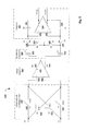
- FIG. 4 a shows a schematic diagram of a switched capacitor sampling network 400 , according to the present disclosure that could be used as an input circuit for an ADC, such as a ⁇ ADC.
- the network 400 comprises a cross-coupled switching circuit 402 comprising a first switch S 1 410 between the first input 446 of the analog differential signal 405 and an input of the first driver amplifier 418 , and a second switch S 2 412 between the second input 448 of the analog differential signal 405 and an input of the second driver amplifier 420 .
- the cross-coupled switching circuit 402 further comprises a third switch S 3 414 between the first input 446 of the analog differential signal 405 and an input of the second driver amplifier 420 , and a fourth switch S 4 416 between the second input 448 of the analog differential signal 405 and an input of the first driver amplifier 418 , wherein the third switch S 3 414 and the fourth switch S 4 416 operate to cross-couple the first input 446 and the second input 448 of the analog differential signal 405 to the second driver amplifier 420 and the first driver amplifier 418 .
- Network 400 further comprises a driver amplifier system 404 of comprising a first driver amplifier 418 downstream of a first branch of the cross-coupled switching circuit 402 and a second driver amplifier 420 downstream of a second branch of the cross-coupled switching circuit 402 . Additionally, the network 400 comprises a sampling capacitor component 406 comprising a first sampling capacitance C 1 422 coupled to the output 445 of the first driver amplifier 418 and a second sampling capacitance C 2 424 coupled to the output 447 of the second driver amplifier 420 .
- the network 400 comprises an integrator 407 comprising an operational amplifier 408 with an inverting terminal 438 and a non-inverting terminal 440 .
- Integrator 407 produces an integrated signal that comprises a positive voltage output signal “Voutp” 442 and a negative voltage output signal “Voutn” 444 .
- a positive voltage integrator feedback capacitor C 4 434 is connected in parallel with operational amplifier 408 between 438 and “Voutp” 442 .
- a negative voltage integrator feedback capacitor C 3 436 is connected in parallel with operational amplifier 408 between 440 and “Voutn” 444 .
- the network 400 comprises summing junction switches S 4 , S 5 , S 6 and S 7 .
- Switch S 4 428 is disposed between C 1 422 and a reference ground.
- Switch S 6 426 is disposed between C 1 422 and inverting terminal 438 of the operational amplifier 408 .
- switch S 5 430 is disposed between C 2 424 and a reference ground.
- Switch S 7 432 is disposed between C 2 424 and non-inverting terminal 440 of the operational amplifier 408 .
- FIG. 4 b illustrates a two-phase non-overlapping clock 450 defined by four clock waveforms: “ ⁇ 1 ” 452 , “ ⁇ 1 d ” 454 , “ ⁇ 2 ” 456 and “ ⁇ 2 d ” 458 .
- the position of each switch at any given time is determined by its corresponding clock waveform.
- a switch is open when its corresponding clock waveform is “off” and a switch is closed when its corresponding clock waveform is “on”.
- the switches could be configured with other relationships between the state of the switches and their corresponding clock waveforms.
- Operation of network 400 can be explained by tracing the circuits that are established in response to the cycling of the clock waveforms of the clock 450 .
- clock waveforms ⁇ 1 452 and ⁇ 1 d 454 cycle to the on state while the clock waveforms ⁇ 2 456 and ⁇ 2 d 458 remain in the off state.
- switches S 4 428 and S 5 430 close.
- switches S 1 410 and S 2 412 close.
- With S 1 410 and S 4 428 closed a circuit is established between the first input 446 i.e., Vp and ground 449 through driver amplifier 418 and C 1 422 .
- This circuit allows the first input 446 i.e., Vp to be sampled as a charge on C 1 422 . Further, this circuit samples a flicker noise Vfp of the driver amplifier 418 as a charge on C 1 422 .
- a circuit is established between the second input 448 i.e., Vn and ground 449 through driver amplifier 420 and C 2 424 . This circuit allows the second input 448 i.e., Vn to be sampled as a charge on C 2 424 . Further, this circuit samples a flicker noise Vfn of the driver amplifier 420 as a charge on C 2 424 .
- clock waveform ⁇ 1 452 cycles to the off state while ⁇ 1 d 454 remains in the on state.
- Clock waveforms ⁇ 2 456 and ⁇ 2 d 458 remain in the off state.
- switches S 4 428 and S 5 430 open. Opening switch S 4 428 breaks the circuit between the first input 446 i.e., Vp and ground 449 . This isolates the charge stored on C 1 422 , thus effectively sampling the first input 446 i.e., Vp and Vfp.
- opening switch S 5 430 breaks the circuit between the second input 448 i.e., Vn and ground 449 . This isolates the charge stored on C 2 424 , thus effectively sampling the second input 448 i.e., Vn and Vfn.
- clock waveform ⁇ 1 d 454 cycles to the off state.
- Clock waveforms ⁇ 1 452 , ⁇ 2 456 and ⁇ 2 d 458 remain in the off state.
- switches S 1 410 and S 2 412 open. By delaying the opening of switches S 1 410 and S 2 412 until after switches S 4 428 and S 5 430 have been opened, and thus isolating the charges stored on C 1 422 and C 2 424 , the sampled signals are unaffected by the charge injections that occur after switches S 4 428 and S 5 430 have been opened.
- clock waveforms ⁇ 2 456 and ⁇ 2 d 458 cycle to the on state while the clock waveforms ⁇ 1 452 and ⁇ 1 d 454 remain in the off state.
- switches S 3 414 and S 4 416 close.
- switches S 6 426 and S 7 432 close. With switches S 6 426 and S 4 416 closed, a circuit is established between the second input 448 i.e., Vn and the inverting terminal 438 of the operational amplifier 408 through driver amplifier 418 and C 1 422 .
- This circuit allows the second input 448 i.e., Vn and the flicker noise Vfp of the driver amplifier 418 to be sampled as a charge on C 1 422 and further enables the total charge Q C1 + on C 1 422 to be transferred to C 4 434 .
- switches S 7 432 and S 3 414 closed a circuit is established between the first input 446 i.e., Vp and the non-inverting terminal 440 of the operational amplifier 408 through driver amplifier 420 and C 2 424 .
- This circuit allows the first input 446 i.e., Vp and the flicker noise Vfn of the driver amplifier 420 to be sampled as a charge on C 2 424 and further enables the total charge Q C2 + on C 2 424 to be transferred to C 3 436 .
- the cross-coupled sampling doubles the effective voltage swing (i.e., Vp ⁇ Vn and Vn ⁇ Vp) across the sampling capacitance C 1 422 and C 2 424 by sampling the differential signal with opposite polarities during the first phase and the second phase, thereby doubling the integrated charge across C 4 434 and C 3 436 , while the thermal noise remains the same.
- This improves the SNR performance of the sampling circuit.
- flicker noise Vfp and Vfn of the buffer amplifiers gets sampled on to the sampling capacitance C 1 422 and C 2 424 with the same polarity during the first phase and the second phase, thereby enabling the cancellation of the flicker noise during the integration phase.
- clock waveform ⁇ 2 456 cycles to the off state, while ⁇ 2 d 458 remains in the on state.
- Clock waveforms ⁇ 1 452 and ⁇ 1 d 454 remain in the off state.
- switches S 6 426 and S 7 432 open. Opening switch S 6 426 breaks the circuit between the first input 446 i.e., Vp and inverting terminal 438 of the operational amplifier 408 . This isolates the charge transferred to C 4 434 .
- opening switch S 7 432 breaks the circuit between Vn the second input 448 i.e., Vp and non-inverting terminal 440 of the operational amplifier 408 . This isolates the charge transferred to C 3 436 .
- clock waveform ⁇ 2 d 458 cycles to the off state.
- Clock waveforms ⁇ 1 452 , ⁇ 1 d 454 and ⁇ 2 456 remain in the off state.
- switches S 3 414 and S 4 416 open. By delaying the opening of switches S 3 414 and S 4 416 until after switches S 7 432 and S 6 426 have been opened, and thus isolating the charges stored on C 4 434 and C 3 436 , the sampled signals are unaffected by the charge injections that occur after switches S 6 426 and S 7 432 have been opened.
- clock waveforms ⁇ 1 452 and ⁇ 1 d 454 cycle to the on state while the clock waveforms ⁇ 2 456 and ⁇ 2 d 458 remain in the off state.
- the response of the network 400 to the on state of ⁇ 1 452 and ⁇ 1 d 454 is identical to the response to the on state at time t 0 as explained above.
- network 400 operates in the manner explained above.
- FIG. 4 c illustrates the amplitude Vdiff (i.e., Vp-Vn), of the differential input signal at the first phase ⁇ 1 and the second phase ⁇ 2 . Since the sampling frequency is much higher than the frequency of the input signal, the amplitude of the differential input signal does not change much between ⁇ 1 and ⁇ 2 , as is shown in FIG. 4 c .
- FIG. 4 d illustrates the amplitudes of the differential output of the driver amplifier during ⁇ 1 and ⁇ 2 .
- the differential output of the driver amplifier has opposite polarities (i.e., A*Vdiff at ⁇ 1 and ⁇ A*Vdiff at ⁇ 2 , where A is the gain of the driver amplifier) in the first phase of operation ⁇ 1 and the second phase of operation ⁇ 2 .
- FIG. 4 e illustrates the amplitudes of the differential driver amplifier output flicker noise and offset during ⁇ 1 and ⁇ 2 .
- the differential driver amplifier output flicker noise and offset have the same polarity (i.e., Vbuf_noise) in the first phase of operation ⁇ 1 and the second phase of operation ⁇ 2 .
- the amplitude of the flicker noise is approximately equal in ⁇ 1 and ⁇ 2 , because flicker noise is a low-frequency noise.
- the clock frequency for the oversampling ADCs is usually much higher that the corner frequency of the flicker noise.
- FIG. 5 shows another embodiment of a switched capacitor sampling network 500 , similar to the switched capacitor sampling network 400 .
- the driver amplifier system 504 comprises a fully differential driver amplifier 518 having two differential inputs 519 and 520 and two differential outputs 542 and 544 .
- the analysis for the switched capacitor sampling network 500 is similar to that explained above for the switched capacitor sampling network 400 .
- FIG. 6 shows an example embodiment, wherein the switched capacitor sampling network 600 , similar to the switched capacitor sampling network 400 , is having their driver amplifiers implemented as source followers 601 and 602 .
- the analysis for the switched capacitor sampling network 600 is similar to that explained above for the switched capacitor sampling network 400 .
- the integrator implementation in FIG. 6 has an advantage in comparison to the integrator in FIG. 4 a and FIG. 5 because it comprises a flicker noise cancellation of the internal flicker noise of the integrator.
- S 5 and S 6 sample the flicker noise of the integrator amplifier and differential input signal during ⁇ 1 .
- S 7 and S 8 enable integration of the inverted differential input signal and cancellation of the integrator flicker noise during ⁇ 2 .
- the switched capacitor integrator could be implemented with other techniques for cancellation or reduction of its internal flicker noise.
- FIG. 7 shows a flowchart illustrating a method 700 for sampling a differential signal, according to one embodiment of the disclosure.
- the method 700 is described here with reference to the switched capacitor sampling network 400 of FIG. 4 a with a first driver amplifier Bufp 418 and a second driver amplifier Bufn 420 , however, the method can also be applied to other switched capacitor sampling networks with a fully differential driver amplifier, as illustrated in FIG. 5 .
- the analog differential signal 405 is received at the first input 446 and second input 448 of a cross-coupled switching circuit 402 .
- a first portion Vp of the analog differential signal 405 from the first input 446 is sampled at a first sampling capacitance C 1 422 in a first phase of operation and generates a first charge transfer to the first sampling capacitance C 1 422 .
- a second portion Vn of the analog differential signal 405 comprising an inverted version of the first portion Vp of the analog differential signal 405 is sampled at the first sampling capacitance C 1 422 in a second phase of operation, resulting in a second charge transfer to the first sampling capacitance C 1 422 .
- the first portion Vp and the second portion Vn of the analog differential signal 405 is provided through the driver amplifier 418 , prior to the first and second charge transfers to the first sampling capacitance C 1 422 .
- the second portion Vn of the analog differential signal 405 from the second input 448 is sampled at the second sampling capacitance C 2 424 in a first phase of operation and generates a first charge transfer to the second sampling capacitance C 2 424 .
- the first portion Vp of the analog differential signal 405 comprising an inverted version of the second portion Vn of the analog differential signal 405 is sampled at the second sampling capacitance C 2 424 in a second phase of operation, resulting in a second charge transfer to the second sampling capacitance C 2 424 .
- the second portion Vn and the first portion Vp of the analog differential signal 405 is provided through the driver amplifier 420 , prior to the first and second charge transfers to the second sampling capacitance C 2 424 .
- the switched capacitor sampling network having the buffer amplifier system downstream of the cross-coupled sampling circuit has many advantages.
- Providing the buffer amplifier downstream of the cross-coupled sampling circuit provides reduced resistance in series with the sampling capacitance and provides an isolation of the sampling capacitors from the input signal source, reducing the load for the input source.
- the efficient flicker noise cancellation enables reduced design requirements for the internal flicker noise of the driver amplifier, thereby making it possible to choose relatively small input transistor dimensions in order to reduce the switched capacitive load for the input signal source.
- the suppression of the flicker noise enables the optimization of the driver amplifier towards low thermal noise, while maintaining small input capacitance.
Landscapes
- Engineering & Computer Science (AREA)
- Theoretical Computer Science (AREA)
- Power Engineering (AREA)
- Amplifiers (AREA)
- Analogue/Digital Conversion (AREA)
Priority Applications (4)
| Application Number | Priority Date | Filing Date | Title |
|---|---|---|---|
| US14/615,001 US9525426B2 (en) | 2015-02-05 | 2015-02-05 | Cross-coupled input voltage sampling and driver amplifier flicker noise cancellation in a switched capacitor analog-to-digital converter |
| CN201610080064.6A CN105871376B (zh) | 2015-02-05 | 2016-02-04 | 开关电容器数模转换器中的电压采样和驱动器放大器闪烁噪声消除 |
| KR1020160013837A KR101721358B1 (ko) | 2015-02-05 | 2016-02-04 | 스위치드 커패시터 아날로그-디지털 컨버터 내의 교차 결합된 입력 전압 샘플링 및 드라이버 증폭기 플릭커 노이즈 상쇄 |
| DE102016102082.6A DE102016102082A1 (de) | 2015-02-05 | 2016-02-05 | Kreuzgekoppelte Eingangsspannungsabtastung und Treiberverstärker-Flicker-Rauschen-Auslöschung in einem Geschalteter-Kondensator-Analog-Digital-Wandler |
Applications Claiming Priority (1)
| Application Number | Priority Date | Filing Date | Title |
|---|---|---|---|
| US14/615,001 US9525426B2 (en) | 2015-02-05 | 2015-02-05 | Cross-coupled input voltage sampling and driver amplifier flicker noise cancellation in a switched capacitor analog-to-digital converter |
Publications (2)
| Publication Number | Publication Date |
|---|---|
| US20160233874A1 US20160233874A1 (en) | 2016-08-11 |
| US9525426B2 true US9525426B2 (en) | 2016-12-20 |
Family
ID=56565457
Family Applications (1)
| Application Number | Title | Priority Date | Filing Date |
|---|---|---|---|
| US14/615,001 Active US9525426B2 (en) | 2015-02-05 | 2015-02-05 | Cross-coupled input voltage sampling and driver amplifier flicker noise cancellation in a switched capacitor analog-to-digital converter |
Country Status (4)
| Country | Link |
|---|---|
| US (1) | US9525426B2 (ko) |
| KR (1) | KR101721358B1 (ko) |
| CN (1) | CN105871376B (ko) |
| DE (1) | DE102016102082A1 (ko) |
Cited By (4)
| Publication number | Priority date | Publication date | Assignee | Title |
|---|---|---|---|---|
| US10291226B1 (en) | 2018-09-27 | 2019-05-14 | IQ-Analog Corporation | Sample-and-hold circuit with enhanced noise limit |
| US11108404B1 (en) | 2020-07-22 | 2021-08-31 | Analog Devices, Inc. | Low noise integrated circuit techniques |
| US20220052707A1 (en) * | 2020-08-14 | 2022-02-17 | Nxp Usa, Inc. | Analog front-end circuit capable of use in a sensor system |
| US11515884B2 (en) | 2021-04-14 | 2022-11-29 | Analog Devices, Inc. | Noise reducing capacitance driver |
Families Citing this family (10)
| Publication number | Priority date | Publication date | Assignee | Title |
|---|---|---|---|---|
| JP6711691B2 (ja) * | 2016-05-17 | 2020-06-17 | アズビル株式会社 | Opアンプおよび電子回路 |
| EP3300251B1 (en) * | 2016-09-27 | 2020-11-18 | ams International AG | Integration circuit and method for providing an output signal |
| US10128859B1 (en) * | 2018-02-20 | 2018-11-13 | Analog Devices Global Unlimited Company | Correlated double sampling analog-to-digital converter |
| KR102160153B1 (ko) * | 2018-10-31 | 2020-09-25 | 성균관대학교 산학협력단 | 스위치드-커패시터 고속 적분장치 및 방법 |
| CN111082806B (zh) * | 2019-12-26 | 2021-11-23 | 北京化工大学 | 一种消除噪声的方法及系统 |
| US11063602B1 (en) * | 2020-02-05 | 2021-07-13 | Analog Devices International Unlimited Company | Switched capacitor circuits |
| CN111865307B (zh) * | 2020-07-09 | 2022-03-01 | 同济大学 | 噪声整形模数转换器 |
| CN111953323B (zh) * | 2020-07-28 | 2022-05-31 | 北京中星微电子有限公司 | 用于采集信号的电路 |
| GB2598121B (en) * | 2020-08-18 | 2022-08-24 | Crypto Quantique Ltd | Fully differential switched capacitor integrator circuit |
| US11418890B1 (en) * | 2021-04-15 | 2022-08-16 | Knowles Electronics, Llc | Digital sensors, electrical circuits and methods |
Citations (7)
| Publication number | Priority date | Publication date | Assignee | Title |
|---|---|---|---|---|
| US5675334A (en) * | 1996-02-12 | 1997-10-07 | Analog Devices, Inc. | Analog to digital conversion system |
| US6411242B1 (en) * | 2000-06-13 | 2002-06-25 | Linear Technology Corporation | Oversampling analog-to-digital converter with improved DC offset performance |
| US6650263B1 (en) * | 2002-11-04 | 2003-11-18 | Analog Devices, Inc. | Differential sampler structures with reduced distortion and current demand |
| US6809672B2 (en) | 2002-03-22 | 2004-10-26 | Broadcom Corporation | Low power, high SNR, high order delta sigma modulator stage having integrators with pipelined cross coupled input circuits |
| US7167119B1 (en) * | 2005-12-20 | 2007-01-23 | Cirrus Logic, Inc. | Delta-sigma modulators with double sampling input networks and systems using the same |
| US7683815B2 (en) | 2007-06-05 | 2010-03-23 | Analog Devices, Inc. | Cross-coupled switched capacitor circuit with a plurality of branches |
| US20160037108A1 (en) * | 2013-07-09 | 2016-02-04 | Panasonic Corporation | Switched capacitor circuit and method for driving the same |
Family Cites Families (8)
| Publication number | Priority date | Publication date | Assignee | Title |
|---|---|---|---|---|
| US5589831A (en) * | 1995-01-30 | 1996-12-31 | Samsung Semiconductor, Inc. | Fully differential flash ADC based on the voltage follower amplifier structure |
| JP2006140600A (ja) * | 2004-11-10 | 2006-06-01 | Fujitsu Ltd | シグマデルタa/d変換器 |
| KR20080075737A (ko) * | 2007-02-13 | 2008-08-19 | 삼성전자주식회사 | 스위치드 커패시터 회로를 이용한 아날로그 디지털 변환방법 및 장치 |
| CN101355351B (zh) * | 2007-07-23 | 2010-06-02 | 杭州中科微电子有限公司 | 一种cmos低功耗、低失调电压、低回程噪声比较器 |
| US7982526B2 (en) * | 2008-09-17 | 2011-07-19 | Qualcomm, Incorporated | Active-time dependent bias current generation for switched-capacitor circuits |
| KR101087246B1 (ko) * | 2009-09-10 | 2011-11-29 | 연세대학교 산학협력단 | 스위치드 커패시터 회로 |
| US8471744B1 (en) * | 2011-12-01 | 2013-06-25 | Hong Kong Applied Science & Technology Research Institute Company, Ltd. | Reduced residual offset sigma delta analog-to-digital converter (ADC) with chopper timing at end of integrating phase before trailing edge |
| US9154155B2 (en) * | 2013-02-27 | 2015-10-06 | Microchip Technology Incorporated | 2-phase switched capacitor flash ADC |
-
2015
- 2015-02-05 US US14/615,001 patent/US9525426B2/en active Active
-
2016
- 2016-02-04 KR KR1020160013837A patent/KR101721358B1/ko active IP Right Grant
- 2016-02-04 CN CN201610080064.6A patent/CN105871376B/zh active Active
- 2016-02-05 DE DE102016102082.6A patent/DE102016102082A1/de not_active Withdrawn
Patent Citations (7)
| Publication number | Priority date | Publication date | Assignee | Title |
|---|---|---|---|---|
| US5675334A (en) * | 1996-02-12 | 1997-10-07 | Analog Devices, Inc. | Analog to digital conversion system |
| US6411242B1 (en) * | 2000-06-13 | 2002-06-25 | Linear Technology Corporation | Oversampling analog-to-digital converter with improved DC offset performance |
| US6809672B2 (en) | 2002-03-22 | 2004-10-26 | Broadcom Corporation | Low power, high SNR, high order delta sigma modulator stage having integrators with pipelined cross coupled input circuits |
| US6650263B1 (en) * | 2002-11-04 | 2003-11-18 | Analog Devices, Inc. | Differential sampler structures with reduced distortion and current demand |
| US7167119B1 (en) * | 2005-12-20 | 2007-01-23 | Cirrus Logic, Inc. | Delta-sigma modulators with double sampling input networks and systems using the same |
| US7683815B2 (en) | 2007-06-05 | 2010-03-23 | Analog Devices, Inc. | Cross-coupled switched capacitor circuit with a plurality of branches |
| US20160037108A1 (en) * | 2013-07-09 | 2016-02-04 | Panasonic Corporation | Switched capacitor circuit and method for driving the same |
Non-Patent Citations (8)
| Title |
|---|
| Berglund, et al.; "On the Realization of Switched-Capacitor Integrators for Sigma-Delta Modulators"; Dec. 21, 2007, p. 1-118. |
| Enz, et al.; "Circuit Techniques for Reducing the Effects of Op-Amp Imperfections: Autozeroing, Correlated Double Sampling, and Chopper Stabilization"; Proceedings of the IEEE, vol. 84, No. 11, Nov. 1996, p. 1584-1614. |
| Fujimori, A Single-Chip Stereo Audio Delta-Sigma A/D Converter with 117 dB Dynamic Range, IEICE Transaction Fundamentals, vol. E83-A, No. 2, Feb. 2000. * |
| Fujimori; "A Single-Chip Stereo Audio Delta-Sigma A/D Converter with 117dB Dynamic Range"; IEICE Trans. Fundamentals, vol. E83-A, No. 2, Feb. 2000, p. 243-251. |
| James Karki; "Fully-Differential Amplifiers"; Texas Instruments Application Report; SLOA054D-Application Report, Jan. 2002; p. 1-28. |
| McCartney et al, A Low-Noise Low-Drift Transducer ADC, IEEE Journal of Solid-State Circuits, vol. 32, No. 7, Jul. 1997. * |
| Min Gyu Kim, et al.; "A 0.9 V 92 dB Double-Sampled Switched-RC Delta-Sigma Audio ADC"; IEEE Journal of Solid-State Circuits, vol. 43, No. 5, May 2008, p. 1195-1206. |
| Schreier, et al.; "Understanding Delta-Sigma Data Converters"; IEEE Press, 2005, p. 287 and 293. |
Cited By (5)
| Publication number | Priority date | Publication date | Assignee | Title |
|---|---|---|---|---|
| US10291226B1 (en) | 2018-09-27 | 2019-05-14 | IQ-Analog Corporation | Sample-and-hold circuit with enhanced noise limit |
| US11108404B1 (en) | 2020-07-22 | 2021-08-31 | Analog Devices, Inc. | Low noise integrated circuit techniques |
| US20220052707A1 (en) * | 2020-08-14 | 2022-02-17 | Nxp Usa, Inc. | Analog front-end circuit capable of use in a sensor system |
| US11588495B2 (en) * | 2020-08-14 | 2023-02-21 | Nxp Usa, Inc. | Analog front-end circuit capable of use in a sensor system |
| US11515884B2 (en) | 2021-04-14 | 2022-11-29 | Analog Devices, Inc. | Noise reducing capacitance driver |
Also Published As
| Publication number | Publication date |
|---|---|
| CN105871376A (zh) | 2016-08-17 |
| US20160233874A1 (en) | 2016-08-11 |
| KR20160096557A (ko) | 2016-08-16 |
| KR101721358B1 (ko) | 2017-03-29 |
| CN105871376B (zh) | 2019-06-21 |
| DE102016102082A1 (de) | 2016-08-25 |
Similar Documents
| Publication | Publication Date | Title |
|---|---|---|
| US9525426B2 (en) | Cross-coupled input voltage sampling and driver amplifier flicker noise cancellation in a switched capacitor analog-to-digital converter | |
| KR101492722B1 (ko) | 스위칭된 캐패시터 적분기용 시스템 및 방법 | |
| Geerts et al. | A high-performance multibit/spl Delta//spl Sigma/CMOS ADC | |
| JP5431577B2 (ja) | シグマ−デルタ変換器及びアナログ−デジタル変換の方法 | |
| KR100794310B1 (ko) | 스위치드 커패시터 회로 및 그것의 증폭 방법 | |
| US9136867B2 (en) | ΔΣ-modulator and ΔΣ-A/D converter | |
| KR20130142952A (ko) | 오버샘플링된 데이터 컨버터를 초핑하는 시스템 및 방법 | |
| TWI451692B (zh) | 擬差動切換電容電路 | |
| US6636084B2 (en) | Sample and hold circuit | |
| CN107835018B (zh) | 电路、模数转换器和方法 | |
| TWI526001B (zh) | 類比數位轉換器 | |
| US9124290B2 (en) | Method and apparatus for separating the reference current from the input signal in sigma-delta converter | |
| US7068198B2 (en) | Double-sampled integrator system and method thereof | |
| GB2458902A (en) | Equalising phase for switched capacitor circuit operation | |
| JP2013229868A (ja) | サンプルホールド回路 | |
| KR101960180B1 (ko) | 연산 증폭기 이득 보상 기능을 가지는 이산-시간 적분기 회로 | |
| US6836228B1 (en) | Analog-to-digital converter with switched integrator | |
| US9729165B2 (en) | Delta-sigma analog-to-digital converter topology with improved distortion performance | |
| Temes et al. | A high-frequency track-and-hold stage with offset and gain compensation | |
| US7880653B2 (en) | Switched-capacitor circuits, integration systems, and methods of operation thereof | |
| CN111446946B (zh) | 一种单端输出的低噪声全差分开关电容滤波器 | |
| US11588495B2 (en) | Analog front-end circuit capable of use in a sensor system | |
| WO2007079259A2 (en) | Output hold circuits for sample-data circuits | |
| US10044368B2 (en) | Sigma delta analog to digital converter | |
| Willis et al. | Zero CVF input current switched-capacitor instrumentation amplifier |
Legal Events
| Date | Code | Title | Description |
|---|---|---|---|
| AS | Assignment |
Owner name: INFINEON TECHNOLOGIES AG, GERMANY Free format text: ASSIGNMENT OF ASSIGNORS INTEREST;ASSIGNORS:STOJANOVIC, SNEZANA;GRECO, PATRIZIA;BACH, ELMAR;REEL/FRAME:034899/0010 Effective date: 20150205 |
|
| STCF | Information on status: patent grant |
Free format text: PATENTED CASE |
|
| FEPP | Fee payment procedure |
Free format text: PAYOR NUMBER ASSIGNED (ORIGINAL EVENT CODE: ASPN); ENTITY STATUS OF PATENT OWNER: LARGE ENTITY |
|
| MAFP | Maintenance fee payment |
Free format text: PAYMENT OF MAINTENANCE FEE, 4TH YEAR, LARGE ENTITY (ORIGINAL EVENT CODE: M1551); ENTITY STATUS OF PATENT OWNER: LARGE ENTITY Year of fee payment: 4 |