US9299448B2 - Wide bandwidth read and write memory system and method - Google Patents
Wide bandwidth read and write memory system and method Download PDFInfo
- Publication number
- US9299448B2 US9299448B2 US13/518,883 US201013518883A US9299448B2 US 9299448 B2 US9299448 B2 US 9299448B2 US 201013518883 A US201013518883 A US 201013518883A US 9299448 B2 US9299448 B2 US 9299448B2
- Authority
- US
- United States
- Prior art keywords
- read
- write
- data
- port
- mode
- Prior art date
- Legal status (The legal status is an assumption and is not a legal conclusion. Google has not performed a legal analysis and makes no representation as to the accuracy of the status listed.)
- Active, expires
Links
Images


Classifications
-
- G—PHYSICS
- G11—INFORMATION STORAGE
- G11C—STATIC STORES
- G11C16/00—Erasable programmable read-only memories
- G11C16/02—Erasable programmable read-only memories electrically programmable
- G11C16/06—Auxiliary circuits, e.g. for writing into memory
- G11C16/26—Sensing or reading circuits; Data output circuits
-
- G—PHYSICS
- G11—INFORMATION STORAGE
- G11C—STATIC STORES
- G11C11/00—Digital stores characterised by the use of particular electric or magnetic storage elements; Storage elements therefor
- G11C11/21—Digital stores characterised by the use of particular electric or magnetic storage elements; Storage elements therefor using electric elements
- G11C11/34—Digital stores characterised by the use of particular electric or magnetic storage elements; Storage elements therefor using electric elements using semiconductor devices
- G11C11/40—Digital stores characterised by the use of particular electric or magnetic storage elements; Storage elements therefor using electric elements using semiconductor devices using transistors
- G11C11/41—Digital stores characterised by the use of particular electric or magnetic storage elements; Storage elements therefor using electric elements using semiconductor devices using transistors forming static cells with positive feedback, i.e. cells not needing refreshing or charge regeneration, e.g. bistable multivibrator or Schmitt trigger
- G11C11/413—Auxiliary circuits, e.g. for addressing, decoding, driving, writing, sensing, timing or power reduction
- G11C11/417—Auxiliary circuits, e.g. for addressing, decoding, driving, writing, sensing, timing or power reduction for memory cells of the field-effect type
- G11C11/419—Read-write [R-W] circuits
-
- G—PHYSICS
- G11—INFORMATION STORAGE
- G11C—STATIC STORES
- G11C16/00—Erasable programmable read-only memories
- G11C16/02—Erasable programmable read-only memories electrically programmable
- G11C16/06—Auxiliary circuits, e.g. for writing into memory
- G11C16/08—Address circuits; Decoders; Word-line control circuits
-
- G—PHYSICS
- G11—INFORMATION STORAGE
- G11C—STATIC STORES
- G11C16/00—Erasable programmable read-only memories
- G11C16/02—Erasable programmable read-only memories electrically programmable
- G11C16/06—Auxiliary circuits, e.g. for writing into memory
- G11C16/10—Programming or data input circuits
-
- G—PHYSICS
- G11—INFORMATION STORAGE
- G11C—STATIC STORES
- G11C7/00—Arrangements for writing information into, or reading information out from, a digital store
- G11C7/10—Input/output [I/O] data interface arrangements, e.g. I/O data control circuits, I/O data buffers
-
- G—PHYSICS
- G11—INFORMATION STORAGE
- G11C—STATIC STORES
- G11C7/00—Arrangements for writing information into, or reading information out from, a digital store
- G11C7/10—Input/output [I/O] data interface arrangements, e.g. I/O data control circuits, I/O data buffers
- G11C7/1075—Input/output [I/O] data interface arrangements, e.g. I/O data control circuits, I/O data buffers for multiport memories each having random access ports and serial ports, e.g. video RAM
-
- G—PHYSICS
- G11—INFORMATION STORAGE
- G11C—STATIC STORES
- G11C8/00—Arrangements for selecting an address in a digital store
- G11C8/16—Multiple access memory array, e.g. addressing one storage element via at least two independent addressing line groups
Definitions
- the present invention generally relates to the field of integrated circuit memory devices and, more particularly, to systems, devices and methods to enhance read/write bandwidth for memory arrays
- the readout circuit may occupy a significant portion of the entire chip area.
- a number of columns are grouped as a logic column, and therefore a number of adjacent memory cells on one row are normally grouped together into a memory cell unit to share one word line or one X address.
- Write or read operations are performed on one single memory cell per cell unit in each clock cycle in the conventional memory array.
- a 512 ⁇ 32 static random access memory (SRAM) normally consists of 128 rows, each of which includes 128 SRAM cells grouped into 32 memory cell units. That is, one memory cell unit corresponds to every four SRAM cells, and the four SRAM cells share one readout circuit.
- an address decoder in an SRAM array receives row and column addresses over the address bus, and decodes the row addresses to enable a word line.
- Data on an input data port is written into one SRAM cell within a cell unit identified by the input column address while the data in the other three SRAM cells in the same memory cell unit remain the same.
- bit lines of all columns are first pre-charged, while the address decoder decodes the received addresses for the read operation. Once the address decoder completes address decoding, one word line is selected to connect the contents of one row of cell units to the bit lines while the pre-charging is terminated. Bit lines of one of the four columns are selected by the column address and then are sensed and amplified, thus completing a read operation.
- a conventional SRAM array having one set of address decoders can only complete one write or one read operation in one clock cycle.
- Multiple-port SRAM can complete multiple write and/or read operations in one clock cycle.
- the enhanced multiple read/write capability often increases the number of word lines and bit lines, SRAM cell area, control circuit complexity, design cost, and manufacturing cost. For example, the area size of a dual port SRAM cell array normally doubles the area size of a single port SRAM cell array.
- the memory device includes a first memory array, a first read port, a second read port, and a control input port.
- the first memory array contains a plurality of memory cells arranged in an array configuration.
- the first read port is configured to read first data from a single memory cell during a single read cycle
- the second read port is configured to read second data from a group of memory cells controlled by a common word line.
- the control input is configured to receive a mode signal indicating a functional mode for the memory device including a first read mode and a second read mode. When the mode signal indicates the first read mode, the first read port is used to read out the first data. When the mode signal indicates the second read mode, the first read port is used to read out the first data and the second read port is used to read out the second data.
- the memory device includes a memory array, a first write port, a second write port, and a control input port.
- the memory array is configured to contain a plurality of memory cells arranged in an array configuration.
- the first write port is configured to write first data into a single memory cell during a single writing cycle
- the second write port is configured to write second data into a group of memory cells controlled by a common word line during the single writing cycle.
- the control input port is configured to receive a mode signal indicating a functional mode for the memory device including a first write mode and a second write mode. When the mode signal indicates the first write mode, the first write port is used to write the first data; when the mode signal indicates the second write mode, the second write port is used to write the second data.
- Another aspect of the present disclosure includes a method for pseudo dual port memory operation of a memory device including a memory array.
- the memory array contains a plurality of memory cells arranged in an array configuration.
- the method includes providing a first address for a first operation and a second address for a second operation during a single clock cycle, and providing a first enable signal to control a first group of memory cells to start the first operation based on the first address.
- the method also includes latching results from the first operation, providing a control signal to switch from the first operation to the second operation, and providing a second enable signal to control a second group of memory cells to start the second operation based on the second address.
- the SRAM device includes a memory array, an address decoder, a read/write control module, a write module, and a read module.
- the memory array is configured to receive word lines and bit lines, the memory array comprising a first number of rows and a second number of columns of memory cells, each row being controlled by a word line, each column being connected by a bit line and a complementary bit line, every third number of adjacent columns being grouped as a logical column corresponding to a bit of data and every third number of adjacent memory cells on one row being grouped as a memory cell unit.
- the address decoder is configured to receive an address bus and to generate a word line and a column select signal.
- the read/write control module configured to receive control signals to generate a write mode control, a write enable and a read enable.
- the write module is configured to receive the write mode control, the write enable, the column address, a first write input and a second write input and to connect to drive the bit lines and complementary bit lines, the write module selects one or more sets of the third number of bit lines and complementary bit lines in every logic column to be written.
- the read module is configured to receive the read enable, the column address, the bit lines and the complementary bit lines and to generate a first read output and a second read output, the read module multiplexing the third number of bit lines and complementary bit lines in every logic column.
- the disclosed systems and methods may significantly enhance read/write bandwidth for memory arrays by using additional input and output ports at the memory peripheral and utilizing the bit lines.
- the disclosed systems and methods also provides a performance similar to that of the conventional two-port memory at a chip-area cost similar to that of the conventional one-port memory.
- Other advantages and applications are obvious to those skilled in the art.
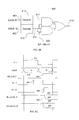
- FIG. 1 illustrates an exemplary block diagram of an input/output interface for a memory array consistent with the disclosed embodiments
- FIG. 1A illustrates an exemplary block diagram of an input/output interface for a memory array consistent with the disclosed embodiments
- FIG. 1B illustrates an exemplary block diagram of a memory array with enhanced bandwidth consistent with the disclosed embodiments
- FIG. 2 illustrates a block diagram of an SRAM array allowing one-bit read/write operation
- FIG. 3A illustrates an exemplary block diagram of a SRAM array performing a write operation consistent with the disclosed embodiments.
- FIG. 3B illustrates a truth table for the write modules consistent with the disclosed embodiments
- FIG. 4A illustrates an exemplary block diagram of the SRAM array in a Wide Bandwidth Read mode for a parallel read operation consistent with the disclosed embodiments
- FIG. 4B illustrates an exemplary block diagram 450 of a SRAM array implemented in the Normal Bandwidth Read mode for sequential read operations consistent with the disclosed embodiments;
- FIG. 5 illustrates a timing diagram 500 of SRAM controls and output signals in a clock cycle in an SRAM array
- FIG. 6A illustrates an exemplary timing diagram of increasing write bandwidth by using two address decoders to add a sequential write operation during a read clock cycle consistent with the disclosed embodiments
- FIG. 6B illustrates an exemplary block diagram of an address decoder receiving two addresses and comprising two decoders to sequentially select one of the two addresses in one clock cycle consistent with the disclosed embodiments;
- FIG. 6C illustrates an exemplary timing diagram of using one address decoder to increase the write bandwidth by adding a write operation during a read clock cycle consistent with the disclosed embodiments
- FIG. 6D illustrates an exemplary block diagram of an address decoder that comprises one decoder for sequentially decoding a write address and a read address from one address in one clock cycle consistent with the disclosed embodiments;
- FIG. 7 illustrates a method for employing one read module to drive two SRAM arrays consistent with the disclosed embodiments.
- FIG. 1B illustrates an exemplary preferred embodiment(s).
- FIG. 1 and FIG. 1A illustrates an exemplary block diagram 100 of an input/output interface for a memory array 102 involving additional input/output ports to enhance the bandwidth for memory write and read operations.
- an address bus 101 provides the memory array 102 with row and column addresses for write or read, and a control line 103 is used to control operations (write or read) and function modes (normal or wide bandwidth).
- a normal bandwidth write port 104 is used to input data for write in a normal bandwidth write mode, and a wide bandwidth write port 105 is used to input multiple data for parallel writes in a wide bandwidth write mode.
- the data in the memory array 102 are read out through a normal bandwidth read port 106 in a normal bandwidth read mode, and through a wide bandwidth read port 107 or a second data read port in a wide bandwidth read mode.
- the bandwidths for read and write operations are enhanced due to the use of the wide bandwidth write and read ports 105 and 107 .
- FIG. 1B illustrates an exemplary block diagram 150 of a memory array with enhanced read and write bandwidths in certain implementations.
- the memory array 102 further comprises of an address decoder 111 , a read/write control module 112 , a write module 114 , memory cells 113 , a read module 115 and a read register module 116 .
- the address decoder 111 receives addresses from the address bus 101 , drives the word line and delivers the column addresses to the write module 114 and the read module 115 and read register module 116 .
- the read/write control module 112 comprises an optional sequential control module, a write control module and a read control module (not shown).
- Read/write control module 112 receives the control line 103 , and generates a read enable, a write enable and a write mode control.
- the write module 114 may receive the write enable, write mode control and column address; and deliver the data input from the normal bandwidth write port 104 or wide bandwidth write port 105 to a selected memory cell or selected memory cells.
- the read module 115 may receive the read enable and column address, and deliver data in a selected memory cell or selected memory cells directly to the normal bandwidth read port 106 or the read register module 116 .
- the read register module 116 may temporarily store the data and deliver the data to the wide bandwidth read port or second data read port 107 .
- the exemplary memory array 150 is written in by two aforementioned write modes, the normal bandwidth write mode and the wide bandwidth write mode.
- the normal bandwidth write mode data coming from the normal bandwidth write port 104 is written to a SRAM cell selected by input row and column addresses. Three unselected SRAM cells in the same memory cell unit have high impedance, and their internal data will not be overwritten.
- write module 114 allows the data in four SRAM cells included in one memory cell unit to be refreshed simultaneously.
- the exemplary memory array 150 is also read out by two aforementioned read modes, normal bandwidth read mode and wide bandwidth read mode.
- the read module 115 comprises low-speed read (sensing) modules and a high-speed read (sensing) module (not shown).
- the high-speed read module requires significantly more chip area than the low-speed read module. Bit lines of each individual SRAM cell are connected with its own low-speed read module for reading multiple SRAM cells in parallel at a relatively low speed, and four SRAM cells in a memory cell unit share a high-speed read module for reading out one of the SRAM cells at a faster speed.
- the high-speed read module first senses and amplifies data from one SRAM cell as specified by the column address.
- the data are outputted to the normal bandwidth read port 106 .
- the high-speed read module outputs the data in the selected SRAM cell to the normal bandwidth read port 106 .
- the data in the other unselected SRAM cells are outputted in parallel to the wide-bandwidth read port 107 using their own low-speed read sensing modules.
- the data in the unselected SRAM cells are stored in the read register module 116 and ready for output sequentially through the second data read port 107 while another row is being read and outputted to normal bandwidth read port 106 in the normal bandwidth read mode. Therefore, by using two read ports, an equivalent configuration of pseudo dual read port memory is formed with a single port memory array to enhance the read bandwidth.
- FIG. 2 illustrates a block diagram 200 of a conventional SRAM array allowing one-bit read/write operation.
- SRAM cells 203 , 204 , 205 and 206 on four different columns are controlled by one common word line WL 0 207
- SRAM cells 222 , 223 , 224 and 225 on four different columns are controlled by another common word line WL 1 217 .
- a write-enable signal WE 226 is enabled, and data are written into a memory cell selected by a column address 228 .
- the column address of “00” selects the SRAM cells 203 or 222 ; the column address of “01” selects the SRAM cells 204 or 223 ; the column address of “10” selects the SRAM cells 205 or 224 ; and the column address of “11” selects the SRAM cells 206 or 225 .
- data are inputted to write modules 208 , 209 , 210 and 211 through the normal bandwidth write port 104 , and further passed to the set of bit lines BL and BL_N (i.e.
- bit line bar the differential signal of BL, as indicated by 218 in FIG. 2 together with the bit line BL) selected by the column address 228 while the unselected three sets of bit lines BL and BL_N are kept high-impedance.
- the column address is “01”
- data are sent to the bit lines 219 which are connected to the SRAM cells 223 and 204 , and the other bit lines 218 , 220 and 221 are kept as high-impedance.
- WL 0 207 is enabled, the data are written into the SRAM cell 204 and the data in all the other SRAM cells remain the same.
- the decoders 212 and 213 receive the column address 228 and select one of the four SRAM cells in the corresponding row.
- the data in the selected SRAM cell is read out by the high speed readout module 214 and output to a normal bandwidth output port 106 .
- FIG. 3A illustrates an exemplary block diagram 300 of a SRAM array which performs a write operation based on one bit of input data.
- FIG. 3A and/or other figures in this disclosure use a same number or label to refer a device or component shown in a conventional device, it is understand that the device or component described in the disclosed embodiments is for the convenience of illustration and is not necessarily identical to the ones shown in the conventional device.
- SRAM cells 203 , 204 , 205 and 206 on four different columns are controlled by one common word line WL 0 207
- SRAM cells 222 , 223 , 224 and 225 on four different columns are controlled by another common word line WL 1 217 .
- Data are written into a memory cell selected by a column address 228 .
- the column addresses of “00”, “01”, “10”, and “11” select SRAM cells 203 or 222 , 204 or 223 , 205 or 224 , and 206 or 225 , respectively.
- a write enable 226 and a write mode control 313 are generated by a write control logic in the read/write control module 112 . In a write operation, the write enable WE 226 is first enabled, and the write mode control 313 is used to select the write mode as the normal bandwidth write mode or the wide bandwidth write mode.
- the write module 114 includes write modules 308 , 309 , 310 and 311 .
- one bit of data are inputted to one of the write modules 308 , 309 , 310 or 311 through a normal bandwidth write port 104 during each write cycle.
- Data are further written to the set of bit lines BL and BL_N selected by the column address 228 while the unselected three sets of bit lines BL and BL_N are connected as high-impedance.
- the word line WL 0 207 is selected and the column address is “01”.
- Data are sent to the bit lines 319 which are connected to the memory cells 223 and 204 , and the other bit lines 318 , 320 and 321 are connected as high-impedance.
- WL 0 is enabled, the data are written into the SRAM cell 204 , and the data in all the other SRAM cells remain the same.
- the wide bandwidth write mode four bits of data are provided to the write modules 308 , 309 , 310 and 311 , respectively, from a wide bandwidth write port 105 .
- Column address 228 is not used in this mode.
- Four bits of data are sent to the bit lines 318 , 319 , 320 and 321 through line A ( 329 ), line B ( 330 ), line C ( 331 ), and line D ( 332 ), respectively.
- the word line WL 0 207 is enabled, the data are written in parallel into the SRAM cells 203 , 204 , 205 and 206 , and the data in SRAM cell 222 , 223 , 224 and 225 remain the same.
- FIG. 3B illustrates a truth table 350 for the write modules in FIG. 3A .
- the write enable WE 226 is disabled (i.e., WE 226 is “0”), and the outputs of the write modules 308 , 309 , 310 , and 311 are all connected as high-impedance (Z).
- both the WE 226 and the write mode control 313 are enabled.
- the wide bandwidth write mode is activated (i.e., write mode control is ‘1’).
- Data and the complimentary data A 328 and A_N 343 , B 329 and B_N 344 , C 330 and C_N 345 , and D 331 and D_N 346 are sent in parallel to the bit lines 318 , 319 , 320 and 321 that are connected to the write modules 308 , 309 , 310 and 311 , respectively.
- the WE 226 is enabled, and the write mode control 313 is disabled.
- the normal bandwidth write mode is activated.
- the column address 228 is “11” as shown in row 362
- the data BIT_IN is inputted from the normal bandwidth write port 104 .
- BIT_IN 341 and the complementary BIT_IN_N 342 are written to the set of bit lines BL and BL_N connected with the SRAM cells 225 and 206 .
- the column address 228 is “00”, “01” or “10” as shown in rows 356 , 358 and 360
- the data BIT_IN are inputted from the normal bandwidth write port 104
- BIT_IN and BIT_IN_N are written to the bit lines BL and BL_N connected with the SRAM cells 222 and 203 , 223 and 204 , or 224 and 205 , respectively.
- Other unaddressed bit lines are kept in high-impedance Z.
- FIG. 4A illustrates an exemplary block diagram 400 of the SRAM array in a wide bandwidth read mode for a parallel read operation.
- SRAM cells 203 , 204 , 205 and 206 on four different columns are controlled by one common word line WL 0 207
- SRAM cells 222 , 223 , 224 and 225 on four different columns are controlled by another common word line WL 1 217 .
- All columns share a high-speed read module 214 , and each column has its own separate low-speed read modules 411 , 412 , 413 and 414 , respectively.
- the high-speed read module 214 consumes a larger chip area than the low-speed read modules 411 , 412 , 413 and 414 although the read speed of 214 is faster than that of the low-speed read modules.
- High-speed read module 214 and low-speed read modules 411 , 412 , 413 and 414 may be included in read module 115 (in FIG. 1B ).
- high speed read module 214 is capable of finishing the read sensing of data on bit lines within the first clock cycle while the read process of low speed read modules 411 , 412 , 413 and 414 takes longer than one clock cycle and therefore may be completed in the second clock cycle.
- data in the SRAM cell 203 are read out to normal bandwidth read port 439 ( 106 in FIG. 1 ) during the first clock cycle, and data in the SRAM cells 204 , 205 and 206 are read out to the wide bandwidth read port 407 ( 107 in FIG. 1 ) during the second clock cycle.
- the word line WL 0 207 is enabled, and the bit lines of the SRAM cell 203 are selected by the multiplexers 212 and 213 as specified by the column address 228 .
- Data in the SRAM cell 203 are directly read to the high speed read module 214 , the sensed and amplified result is outputted on bus 439 . While the data in the SRAM cell 203 is read by high speed read module 214 , the data from the SRAM cells 203 , 204 , 205 and 206 are also sensed, and amplified by the low speed read modules 414 , 411 , 412 , and 413 .
- the word line WL 0 207 remains enabled, the signals in the SRAM cells 203 , 204 , 205 and 206 are still sensed and amplified by the low-speed read modules 414 , 411 , 412 and 413 if the sensing process is not completed in the first clock cycle.
- the signals 415 , 418 , 419 , and 420 are outputted in parallel to the wide bandwidth read port 407 .
- Signal 415 may also be provided by read module 414 to the wide bandwidth read port 407 , but may be ignored because the SRAM cell 203 is already read during the first clock cycle.
- data in each of SRAM cells 203 , 204 , 205 , and 206 may also be read out through high speed read module 214 during the first clock cycles while the remaining data in remaining cells are read out in the second clock cycles.
- wide bandwidth read port 407 may be controlled by a read control module to output a particular signal 415 , 418 , 419 , or 420 .
- wide bandwidth read port 407 may provide all signals 415 , 418 , 419 , and 420 , and an outside multiplexer may be used to select a particular signal 415 , 418 , 419 , or 420 .
- Other configurations may also be used.
- FIG. 4B illustrates an exemplary block diagram 450 of a SRAM array implemented in the wide bandwidth read mode for sequential read operations.
- SRAM cells 203 , 204 , 205 and 206 in four different columns are controlled by one common word line WL 0 207
- SRAM cells 222 , 223 , 224 and 225 on four different columns are controlled by another common word line WL 1 217 .
- all columns share a high-speed read module 214 , and each column has its separate low-speed read modules 411 , 412 , 413 and 414 , respectively.
- the high speed read module 214 is capable of completing the read sensing of data on bit lines within a first clock cycle while the read process of low speed read modules 411 , 412 , 413 and 414 takes longer than one clock cycle and therefore may be completed in a second clock cycle.
- Latches 421 , 422 , 423 , and 424 are provided to latch outputs from low speed read modules 411 , 412 , 413 and 414 , respectively.
- the WL 0 207 is enabled.
- the SRAM cell 203 is then selected by the column address 228 using the two-bit multiplexers 212 and 213 , and the data in SRAM cell 203 is sent to the high speed read module 214 and the output signal is then provided to the normal bandwidth data port 439 ( 106 in FIG. 1 ).
- SRAM cell 203 is read out during the first clock cycle on normal bandwidth data port 439 ( 106 in FIG. 1 ).
- the data from the SRAM cells 203 , 204 , 205 and 206 are also sensed, and amplified by the low speed read modules 414 , 412 , 412 and 413 .
- the word line WL 0 207 remains enabled, the signals in the SRAM cells 203 , 204 , 205 and 206 are still sensed and amplified by the low-speed read modules 414 , 411 , 412 and 413 if the sensing process is not completed in the first clock cycle.
- the read out data in the low-speed read modules 414 , 411 , 412 and 413 are held in the latches 421 , 422 , 423 and 424 , respectively.
- the read control module 416 controls the multiplexer 409 to output the data held in latch 422 (content of memory cell 204 ) to a second data read port 440 (e.g., wide bandwidth read port 107 in FIG. 1 ).
- SRAM cell 204 is read out during the second clock cycle on second data read port 440 (i.e. wide bandwidth data port 107 in FIG. 1 ) through multiplexer 409 under the multiplexer control signal generated by read control module 416 .
- the WL 0 207 is no longer enabled, and the read control module 416 controls the multiplexer 409 to output the data held by the latch 423 to the second data read port 440 directly.
- content of SRAM cell 205 is read out during the third clock cycle on second data read port 440 (i.e. wide bandwidth data port 107 in FIG. 1 ).
- another word line e.g., WL 1 217
- a second data from another SRAM cell on another row e.g., SRAM cell 223
- normal bandwidth data port 439 i.e. 106 in FIG. 1
- the read control module 416 controls the multiplexer 409 to output the data (SRAM cell 206 ) in the latch 424 directly to the second data read port 440 . Therefore, by the end of the fourth clock cycle, the data in the memory cells 203 , 204 , 205 and 206 are read out sequentially within four consecutive clock cycles from the normal bandwidth data port 439 ( 106 in FIG. 1 ) and the second data read port 440 ( 107 in FIG. 1 ).
- the WL 0 207 can be disabled in the third clock cycle, bit lines BL and BL_N may be pre-charged, and the next word line WL 1 217 may be enabled.
- the SRAM cell 223 is then selected by the column address 228 using the multiplexer 212 and 213 , and the data in the SRAM cell 223 are outputted to the high speed read module 214 and then to the normal bandwidth data port 439 (i.e. 106 in FIG. 1 ).
- the bus 440 i.e. wide bandwidth data port 107 in FIG.
- each data of memory cells 203 , 204 , 205 and 206 may be outputted to bus 440 ( 107 in FIG. 1 ) under the multiplexer 409 control signal generated by read control module 416 .
- read control module 416 updates the latches 421 , 422 , 423 and 424 to latch in the sensed and read memory contents of memory cells 222 , 223 , 224 , and 225 .
- data of either memory cells 222 , 223 , 224 or 225 may be outputted to bus 440 ( 107 in FIG. 1 ) through multiplexer 409 under the multiplexer control signal generated by read control module 416 .
- bus 440 107 in FIG. 1
- multiplexer 409 under the multiplexer control signal generated by read control module 416 .
- the write/read bandwidths are further enhanced by applying the sequential read/write control module which allows a write operation to follow a read operation within one clock cycle, thus may form pseudo dual read/write ports.
- All bit lines are pre-charged while the address decoder first decodes the read addresses. Upon generating the read addresses, the pre-charging is terminated and the word line is enabled. The read module captures the data and is then disconnected from the selected bit lines. While the read module goes on to amplify the captured data, the write-enable signal becomes valid and the write address is decoded to enable a word line for write. Data are written into the selected bit line by a write module.
- the write operation may be done to either the same cells on the same word line with the cells being read out or cells on different word lines.
- the read operation in the above-mentioned write-after-read operation can be substituted with another write operation, and thus two write operations in one clock cycle using the same or similar control mechanism.
- FIG. 5 illustrates a timing diagram 500 of SRAM control signals and output signals in a clock cycle in the SRAM array as shown in FIG. 2 .
- CLK 501 is a clock signal
- ADDRESS 502 is an address bus signal.
- WL 503 is the word line signal for the SRAM cells. WL 503 is enabled after the address decoder decodes ADDRESS 502 and is disabled at falling edge of the clock cycle CLK 501 . Assuming the data contained in the SRAM cell is “1”. Bit lines BL 504 and BL_N 505 are pre-charged to high till the ADDRESS 502 is decoded and the WL 503 is enabled.
- the BL remains at a high level while BL_N 505 is slowly pulled down by the content of the SRAM cell.
- a read circuit samples and amplifies the levels of the BL 504 and BL_N 505 at sampling time 506 to produce read out data SA 507 and SA_N 508 .
- the BL 504 and BL_N 505 are disconnected from the read circuit.
- a digital level of “high” is properly outputted from the signals SA 507 and SA_N 508 .
- FIG. 6A illustrates an exemplary timing diagram 600 of increasing write bandwidth by using two address decoders to add a write operation in a read clock cycle such that a read operation and a write operation can be performed in one clock cycle.
- CLK 501 is the clock signal.
- ADDR_R 601 is a first address signal for the read operation.
- ADDR_W 602 is a second address signal for the write operation.
- WL_R 604 is a word line signal enabling a row of SRAM cells for read.
- WL_W 605 is a word line signal enabling a row of SRAM cells for write.
- WE_DELAY 603 is the write mode control signal.
- BL 606 and BL_N 607 are pre-charged to “1” at the beginning of the read clock cycle, and the pre-charge completes before ADDR_R 601 is decoded and WL_R 604 is enabled. Data in BL_N 607 slowly drops in order to restore to “0”.
- the read module 214 senses and amplifies the data in the BL 606 and BL_N 607 to be SA 608 and SA_N 609 , and then disconnect from the BL 606 and BL_N 607 . Subsequently, WE_DELAY 603 is enabled and ADDR_W 601 has already been decoded.
- Data “0” and “1” to be written are sent to BL 606 and BL_N 607 , respectively.
- the write drivers which drive the bit lines in this embodiment has both a pull up and pull down capability, thus the write action is not limited to after a bit lines pre-charging.
- BL 606 is immediately pulled down and BL_N 607 is pulled up.
- Read out data “1” has already been properly sampled, sensed and outputted from the SA 608 , and the write-indata “0” is properly written to the BL 606 as well.
- the SRAM array can read data first and then write data. Alternatively, the read can also be replaced with a write so that two write operations happen sequentially, no bit liens pre-charging necessary between the two write actions, thus may form pseudo dual write ports.
- FIG. 6A illustrates an exemplary timing diagram 600 of increasing write bandwidth by using two address decoders to add a write operation in a read clock cycle such that a read operation and a write operation can be performed in one clock cycle.
- CLK 501 is the clock signal.
- ADDR_R 601 is a first address signal for the read operation.
- ADDR_W 602 is a second address signal for the write operation.
- WE_DELAY 603 is the delay write enable control signal which enables the write word line after a certain delay in timing.
- WL_R 604 is a read word line for a row of SRAM cells being read.
- WL_R 604 is active after the decoding of the read address 601 and is disabled before WE_DELAY 603 is active.
- WL_W 605 is a word line signal selecting a row of SRAM cells for write.
- WL_W 605 is enabled after WE_DELAY 603 is active and is disabled before the next rising edge of CLK 501 .
- BL 606 and BL_N 607 are pre-charged to “1” at the beginning of the read clock cycle, and the pre-charge is completed before ADDR_R 601 is decoded and WL_R 604 is enabled.
- WL_R 604 is active.
- BL_N 607 is slowly pulled down by memory cell controlled by WL_R 604 .
- the read module 214 senses the data on BL 606 and BL_N 607 and later amplifies the data to be read out as “1” on SA and SA_N ports. Also, at sampling time the read module 214 are disconnected from the BL 606 and BL_N 607 .
- BL 606 and BL_N 607 are written on to BL 606 and BL_N 607 , respectively.
- BL 606 is immediately pulled down and BL_N 607 is pulled up.
- WE_DELAY 603 enabled the word line WL_W 605 which is selected by the write address decoder through decoding ADDR_W 602 .
- a data “0” is then stored on the memory cell on bit line BL 606 and BL_N 607 , which is enabled by word line WL_W 605 .
- the SRAM array can read data first and then write data in the same clock cycle.
- the read operation can also be replaced by a write operation so that two write operations can be performed in the same clock cycle, thus may form pseudo dual write ports.
- FIG. 6B illustrates an exemplary block diagram 650 of an address decoder receiving two addresses and comprising two decoders to sequentially select one of the two addresses in one clock cycle.
- the word lines for read 611 are decoded from ADDR_R 601 by a decoder 610
- the word lines for write 612 are decoded from ADDR_W 602 by a decoder 615 .
- the word line read selection signal 611 is outputted as target word lines 613 to allow reading from a particular target row.
- WE_DELAY 603 is enabled, the word line write selection signal 612 is outputted as the target word lines 613 to allow writing to the target SRAM cell. Read and write operations may be targeted to different rows.
- FIG. 6C illustrates an exemplary timing diagram of using one address decoder to increase the write bandwidth by adding a write operation during a read clock cycle.
- the sequential read and write operations are the same as in FIG. 6A , except that read and write addresses are inputted sequentially on one address bus ADDR 632 .
- the read address is decoded from ADDR 632 before WL_R 604 is enabled, and later in the clock cycle, the write address is decoded from ADDR 632 before WL_W 605 is enabled.
- the read and write operations can be performed on the same SRAM cell (the read address and write address are the same) or on two different SRAM cells (the read address and write address are different from each other).
- FIG. 6D illustrates an exemplary block diagram 680 of an address decoder that comprises one decoder for sequentially decoding a write address and a read address from one address ADDR 616 in one clock cycle as in FIG. 6C .
- decoder 610 is coupled to a plurality of pass gates, for example, pass gates 620 , 621 , 622 and 623 , and an output end of each pass gate is connected to ground through a NMOS transistor.
- bit lines are pre-charged, and the pass gates 620 , 621 , 622 and 623 are at first closed.
- the NMOS transistors 624 , 625 , 626 and 627 are enabled to set “0” to all word lines.
- a read address inputted through the address bus ADDR 616 is decoded by the decoder 610 .
- the decoding results are passing through the pass gates 620 , 621 , 622 and 623 which are enabled by enable signal 618 to enable a word line in word lines 613 for reading.
- the pass gates 620 , 621 , 622 and 623 are disabled and the NMOS transistors 624 , 625 , 626 and 627 are turned on again to discharge the word line previous charged for reading.
- the pass gates 620 , 621 , 622 and 623 are turned on again, this time passing the write word line selection signal generated by decoder 610 based on the write address on ADDR 632 , to enable one of the word lines in 613 to select a row of memory cells for writing.
- write or read operations can be performed on SRAM cells on two different rows.
- FIG. 7 illustrates a method for employing one read module to serve two SRAM arrays.
- the bit lines of two separate SRAM arrays 705 and 706 having the same column address are multiplexed by an array multiplexer included in the read module 702 .
- the array multiplexer is controlled by a select signal, selecting data on either bit lines 705 or 706 for sensing and amplifying.
- a write operation may be performed on one of SRAM array 705 or 706 while either a write or a read operation may be performed on the other SRAM array 706 or 705 .
- both SRAM arrays are under write operations.
- One word line 703 in the SRAM array 705 is enabled, and data are written into the cells controlled by 703 through a write port 708 ; at the same time, another word line 711 is enabled in the SRAM array 706 , and data are written into the cells controlled by word line 711 through a write port 709 .
- a read and a separate write operation are performed on the SRAM arrays 705 and 706 , respectively.
- the word line 703 in the SRAM array 705 is enabled, and data in memory cells controlled by word line 703 are read out by a read module 702 to a read port 704 ; at the same time, the word line 711 is enabled in the SRAM array 706 , and data are written into cells controlled by 711 through the write port 709 .
- the write port can be either the normal or the wide bandwidth write port, and the read ports can be either the normal or the wide bandwidth read port.
- the disclosed devices and methods may be used in various applications in stand-alone memory devices and embedded memory devices in processors, SOC chips, computing systems, communication and other digital systems.
- the disclosed devices and methods may be used in high performance processor cache applications, high-efficient data processing applications crossing multiple levels of memory hierarchy or even crossing multiple levels of networked systems.
Landscapes
- Engineering & Computer Science (AREA)
- Microelectronics & Electronic Packaging (AREA)
- Computer Hardware Design (AREA)
- Multimedia (AREA)
- Static Random-Access Memory (AREA)
Applications Claiming Priority (4)
| Application Number | Priority Date | Filing Date | Title |
|---|---|---|---|
| CN200910247456.7A CN102110464B (zh) | 2009-12-26 | 2009-12-26 | 宽带读写存储器装置 |
| CN200910247456.7 | 2009-12-28 | ||
| CN200910247456 | 2009-12-28 | ||
| PCT/CN2010/080378 WO2011079780A1 (en) | 2009-12-26 | 2010-12-28 | Wide bandwidth read and write memory system and method |
Publications (2)
| Publication Number | Publication Date |
|---|---|
| US20120265951A1 US20120265951A1 (en) | 2012-10-18 |
| US9299448B2 true US9299448B2 (en) | 2016-03-29 |
Family
ID=44174594
Family Applications (1)
| Application Number | Title | Priority Date | Filing Date |
|---|---|---|---|
| US13/518,883 Active 2033-02-18 US9299448B2 (en) | 2009-12-26 | 2010-12-28 | Wide bandwidth read and write memory system and method |
Country Status (4)
| Country | Link |
|---|---|
| US (1) | US9299448B2 (zh) |
| EP (1) | EP2519951A4 (zh) |
| CN (1) | CN102110464B (zh) |
| WO (1) | WO2011079780A1 (zh) |
Families Citing this family (17)
| Publication number | Priority date | Publication date | Assignee | Title |
|---|---|---|---|---|
| CN102541462A (zh) * | 2010-12-28 | 2012-07-04 | 上海芯豪微电子有限公司 | 宽带读写存储器装置 |
| CN102637449A (zh) * | 2012-04-13 | 2012-08-15 | 中国科学院微电子研究所 | 一种伪差分式存储阵列 |
| CN103106918B (zh) * | 2012-12-24 | 2015-12-02 | 西安华芯半导体有限公司 | 一种使用单端口存储单元的两端口静态随机存储器 |
| CN106716383B (zh) * | 2014-09-15 | 2021-01-22 | 爱德斯托科技有限公司 | 存储器装置和控制存储器装置的方法、存储器系统 |
| KR102313017B1 (ko) * | 2015-08-21 | 2021-10-18 | 삼성전자주식회사 | 불휘발성 메모리 장치 및 불휘발성 메모리 장치의 쓰기를 제어하는 컨트롤러를 포함하는 스토리지 장치 및 스토리지 장치의 동작 방법 |
| US10061542B2 (en) | 2015-09-15 | 2018-08-28 | Qualcomm Incorporated | Pseudo dual port memory |
| US9406375B1 (en) | 2015-12-04 | 2016-08-02 | International Business Machines Corporation | Write address synchronization in 2 read/1write SRAM arrays |
| CN108074606B (zh) * | 2016-11-10 | 2019-11-29 | 上海磁宇信息科技有限公司 | 一种准多口mram芯片及其读写方法 |
| CN108154226B (zh) * | 2016-12-06 | 2021-09-03 | 上海磁宇信息科技有限公司 | 一种使用模拟计算的神经网络芯片 |
| CN108154225B (zh) * | 2016-12-06 | 2021-09-03 | 上海磁宇信息科技有限公司 | 一种使用模拟计算的神经网络芯片 |
| FR3088767B1 (fr) * | 2018-11-16 | 2022-03-04 | Commissariat Energie Atomique | Circuit memoire adapte a mettre en oeuvre des operations de calcul |
| DE102019128331A1 (de) | 2019-08-29 | 2021-03-04 | Taiwan Semiconductor Manufacturing Co., Ltd. | Gemeinsam genutzter decodiererschaltkreis und verfahren |
| CN112447218A (zh) * | 2019-08-29 | 2021-03-05 | 台湾积体电路制造股份有限公司 | 存储器电路和方法 |
| CN111599391B (zh) * | 2020-05-25 | 2022-03-22 | 无锡中微亿芯有限公司 | 基于动态可重配技术的可扩展多端口块状存储单元 |
| CN111814418A (zh) * | 2020-06-30 | 2020-10-23 | 京微齐力(北京)科技有限公司 | 一种fpga配置存储器 |
| CN111863071B (zh) * | 2020-07-22 | 2022-12-06 | 上海高性能集成电路设计中心 | 一种基于sram实现存内运算的电路结构 |
| US11398274B2 (en) * | 2020-08-25 | 2022-07-26 | Qualcomm Incorporated | Pseudo-triple-port SRAM |
Citations (8)
| Publication number | Priority date | Publication date | Assignee | Title |
|---|---|---|---|---|
| US4541075A (en) * | 1982-06-30 | 1985-09-10 | International Business Machines Corporation | Random access memory having a second input/output port |
| US4933909A (en) * | 1988-12-19 | 1990-06-12 | Bull Hn Information Systems Inc. | Dual read/write register file memory |
| US5422858A (en) * | 1993-06-28 | 1995-06-06 | Hitachi, Ltd. | Semiconductor integrated circuit |
| US6288970B1 (en) * | 1997-10-16 | 2001-09-11 | Altera Corporation | Programmable logic device memory array circuit having combinable single-port memory arrays |
| US6359813B1 (en) * | 1999-11-22 | 2002-03-19 | Fujitsu Limited | Semiconductor memory device having improved data transfer rate without providing a register for holding write data |
| US20050213419A1 (en) * | 2004-03-29 | 2005-09-29 | Sanyo Electric Co., Ltd. | Memory |
| US20070109909A1 (en) * | 2005-11-17 | 2007-05-17 | Jung Chang H | Pseudo-dual port memory where ratio of first to second memory access is clock duty cycle independent |
| US20080052565A1 (en) * | 2006-08-23 | 2008-02-28 | Nec Electronics Corporation | Data read-out circuit in semiconductor memory device and method of data reading in semiconductor memory device |
Family Cites Families (9)
| Publication number | Priority date | Publication date | Assignee | Title |
|---|---|---|---|---|
| US4639890A (en) * | 1983-12-30 | 1987-01-27 | Texas Instruments Incorporated | Video display system using memory with parallel and serial access employing selectable cascaded serial shift registers |
| JPS62229600A (ja) * | 1986-03-31 | 1987-10-08 | Toshiba Corp | 不揮発性半導体記憶装置 |
| DE4408695C1 (de) * | 1994-03-15 | 1995-06-22 | Michael Marks | Mehrtorige Datenspeicheranordnung und Verfahren zum Betrieb derselben |
| US5847994A (en) * | 1997-09-08 | 1998-12-08 | Mitsubishi Denki Kabushiki Kaisha | Non-volatile semiconductor memory device having a back ground operation mode |
| JP3344331B2 (ja) * | 1998-09-30 | 2002-11-11 | 日本電気株式会社 | 不揮発性半導体記憶装置 |
| US6078532A (en) * | 1999-02-01 | 2000-06-20 | Cisco Technology Inc. | Method and apparatus for improving performance of DRAM subsystems with SRAM overlays |
| JP2005004835A (ja) * | 2003-06-10 | 2005-01-06 | Toshiba Corp | 半導体記憶装置 |
| JP4731152B2 (ja) * | 2004-10-29 | 2011-07-20 | ルネサスエレクトロニクス株式会社 | 半導体記憶装置 |
| CN101203919A (zh) * | 2005-03-04 | 2008-06-18 | 爱特梅尔公司 | 用于寄存器文件的快速读取端口 |
-
2009
- 2009-12-26 CN CN200910247456.7A patent/CN102110464B/zh active Active
-
2010
- 2010-12-28 EP EP10840568.9A patent/EP2519951A4/en not_active Withdrawn
- 2010-12-28 WO PCT/CN2010/080378 patent/WO2011079780A1/en active Application Filing
- 2010-12-28 US US13/518,883 patent/US9299448B2/en active Active
Patent Citations (8)
| Publication number | Priority date | Publication date | Assignee | Title |
|---|---|---|---|---|
| US4541075A (en) * | 1982-06-30 | 1985-09-10 | International Business Machines Corporation | Random access memory having a second input/output port |
| US4933909A (en) * | 1988-12-19 | 1990-06-12 | Bull Hn Information Systems Inc. | Dual read/write register file memory |
| US5422858A (en) * | 1993-06-28 | 1995-06-06 | Hitachi, Ltd. | Semiconductor integrated circuit |
| US6288970B1 (en) * | 1997-10-16 | 2001-09-11 | Altera Corporation | Programmable logic device memory array circuit having combinable single-port memory arrays |
| US6359813B1 (en) * | 1999-11-22 | 2002-03-19 | Fujitsu Limited | Semiconductor memory device having improved data transfer rate without providing a register for holding write data |
| US20050213419A1 (en) * | 2004-03-29 | 2005-09-29 | Sanyo Electric Co., Ltd. | Memory |
| US20070109909A1 (en) * | 2005-11-17 | 2007-05-17 | Jung Chang H | Pseudo-dual port memory where ratio of first to second memory access is clock duty cycle independent |
| US20080052565A1 (en) * | 2006-08-23 | 2008-02-28 | Nec Electronics Corporation | Data read-out circuit in semiconductor memory device and method of data reading in semiconductor memory device |
Also Published As
| Publication number | Publication date |
|---|---|
| EP2519951A4 (en) | 2015-06-17 |
| CN102110464A (zh) | 2011-06-29 |
| WO2011079780A1 (en) | 2011-07-07 |
| US20120265951A1 (en) | 2012-10-18 |
| EP2519951A1 (en) | 2012-11-07 |
| CN102110464B (zh) | 2015-06-10 |
Similar Documents
| Publication | Publication Date | Title |
|---|---|---|
| US9299448B2 (en) | Wide bandwidth read and write memory system and method | |
| US7230869B1 (en) | Method and apparatus for accessing contents of memory cells | |
| KR100305549B1 (ko) | 신호전송시스템,신호전송시스템의리시버회로및신호전송시스템이적용되는반도체기억장치 | |
| US4987559A (en) | Semiconductor memory device having a plurality of access ports | |
| JP4083944B2 (ja) | 半導体記憶装置 | |
| US8699289B2 (en) | Techniques for reducing disturbance in a semiconductor memory device | |
| US7447109B2 (en) | Semiconductor storage device | |
| US6768692B2 (en) | Multiple subarray DRAM having a single shared sense amplifier | |
| US6324110B1 (en) | High-speed read-write circuitry for semi-conductor memory | |
| EP1287531B1 (en) | Transparent continuous refresh ram cell architecture | |
| US7653780B2 (en) | Semiconductor memory device and control method thereof | |
| US7349289B2 (en) | Two-bit per I/O line write data bus for DDR1 and DDR2 operating modes in a DRAM | |
| KR20040022378A (ko) | 리프레시 동작이 필요한 반도체 기억 장치 | |
| US7940546B2 (en) | ROM array | |
| US5801996A (en) | Data path for high speed high bandwidth DRAM | |
| TWI683310B (zh) | 波管線 | |
| KR100652295B1 (ko) | 반도체 메모리장치 | |
| US7016235B2 (en) | Data sorting in memories | |
| JP2004310904A (ja) | 不揮発性半導体記憶装置 | |
| US6067274A (en) | Semiconductor memory device having a burst mode | |
| US7027347B2 (en) | Semiconductor memory device | |
| US6785187B2 (en) | Semiconductor device having integrated memory and logic | |
| JPH1166850A (ja) | 半導体記憶装置 | |
| US6678201B2 (en) | Distributed FIFO in synchronous memory | |
| US11676657B2 (en) | Time-interleaving sensing scheme for pseudo dual-port memory |
Legal Events
| Date | Code | Title | Description |
|---|---|---|---|
| AS | Assignment |
Owner name: SHANGHAI XIN HAO MICRO ELECTRONICS CO. LTD., CHINA Free format text: ASSIGNMENT OF ASSIGNORS INTEREST;ASSIGNORS:LIN, KENNETH CHENGHAO;ZHANG, BINGCHUN;REEL/FRAME:028432/0331 Effective date: 20120615 |
|
| STCF | Information on status: patent grant |
Free format text: PATENTED CASE |
|
| MAFP | Maintenance fee payment |
Free format text: PAYMENT OF MAINTENANCE FEE, 4TH YR, SMALL ENTITY (ORIGINAL EVENT CODE: M2551); ENTITY STATUS OF PATENT OWNER: SMALL ENTITY Year of fee payment: 4 |
|
| MAFP | Maintenance fee payment |
Free format text: PAYMENT OF MAINTENANCE FEE, 8TH YR, SMALL ENTITY (ORIGINAL EVENT CODE: M2552); ENTITY STATUS OF PATENT OWNER: SMALL ENTITY Year of fee payment: 8 |