US9293391B2 - Semiconductor module cooler and semiconductor module - Google Patents
Semiconductor module cooler and semiconductor module Download PDFInfo
- Publication number
- US9293391B2 US9293391B2 US14/351,033 US201214351033A US9293391B2 US 9293391 B2 US9293391 B2 US 9293391B2 US 201214351033 A US201214351033 A US 201214351033A US 9293391 B2 US9293391 B2 US 9293391B2
- Authority
- US
- United States
- Prior art keywords
- flow path
- refrigerant
- water jacket
- flow
- flow velocity
- Prior art date
- Legal status (The legal status is an assumption and is not a legal conclusion. Google has not performed a legal analysis and makes no representation as to the accuracy of the status listed.)
- Active
Links
Images


Classifications
-
- H—ELECTRICITY
- H01—ELECTRIC ELEMENTS
- H01L—SEMICONDUCTOR DEVICES NOT COVERED BY CLASS H10
- H01L23/00—Details of semiconductor or other solid state devices
- H01L23/34—Arrangements for cooling, heating, ventilating or temperature compensation ; Temperature sensing arrangements
- H01L23/46—Arrangements for cooling, heating, ventilating or temperature compensation ; Temperature sensing arrangements involving the transfer of heat by flowing fluids
- H01L23/473—Arrangements for cooling, heating, ventilating or temperature compensation ; Temperature sensing arrangements involving the transfer of heat by flowing fluids by flowing liquids
-
- F—MECHANICAL ENGINEERING; LIGHTING; HEATING; WEAPONS; BLASTING
- F28—HEAT EXCHANGE IN GENERAL
- F28F—DETAILS OF HEAT-EXCHANGE AND HEAT-TRANSFER APPARATUS, OF GENERAL APPLICATION
- F28F3/00—Plate-like or laminated elements; Assemblies of plate-like or laminated elements
- F28F3/02—Elements or assemblies thereof with means for increasing heat-transfer area, e.g. with fins, with recesses, with corrugations
-
- F—MECHANICAL ENGINEERING; LIGHTING; HEATING; WEAPONS; BLASTING
- F28—HEAT EXCHANGE IN GENERAL
- F28F—DETAILS OF HEAT-EXCHANGE AND HEAT-TRANSFER APPARATUS, OF GENERAL APPLICATION
- F28F3/00—Plate-like or laminated elements; Assemblies of plate-like or laminated elements
- F28F3/12—Elements constructed in the shape of a hollow panel, e.g. with channels
-
- F—MECHANICAL ENGINEERING; LIGHTING; HEATING; WEAPONS; BLASTING
- F28—HEAT EXCHANGE IN GENERAL
- F28F—DETAILS OF HEAT-EXCHANGE AND HEAT-TRANSFER APPARATUS, OF GENERAL APPLICATION
- F28F9/00—Casings; Header boxes; Auxiliary supports for elements; Auxiliary members within casings
- F28F9/02—Header boxes; End plates
- F28F9/026—Header boxes; End plates with static flow control means, e.g. with means for uniformly distributing heat exchange media into conduits
-
- H—ELECTRICITY
- H01—ELECTRIC ELEMENTS
- H01L—SEMICONDUCTOR DEVICES NOT COVERED BY CLASS H10
- H01L23/00—Details of semiconductor or other solid state devices
- H01L23/34—Arrangements for cooling, heating, ventilating or temperature compensation ; Temperature sensing arrangements
- H01L23/36—Selection of materials, or shaping, to facilitate cooling or heating, e.g. heatsinks
- H01L23/373—Cooling facilitated by selection of materials for the device or materials for thermal expansion adaptation, e.g. carbon
- H01L23/3735—Laminates or multilayers, e.g. direct bond copper ceramic substrates
-
- H—ELECTRICITY
- H05—ELECTRIC TECHNIQUES NOT OTHERWISE PROVIDED FOR
- H05K—PRINTED CIRCUITS; CASINGS OR CONSTRUCTIONAL DETAILS OF ELECTRIC APPARATUS; MANUFACTURE OF ASSEMBLAGES OF ELECTRICAL COMPONENTS
- H05K7/00—Constructional details common to different types of electric apparatus
- H05K7/20—Modifications to facilitate cooling, ventilating, or heating
- H05K7/2089—Modifications to facilitate cooling, ventilating, or heating for power electronics, e.g. for inverters for controlling motor
- H05K7/20927—Liquid coolant without phase change
-
- H—ELECTRICITY
- H01—ELECTRIC ELEMENTS
- H01L—SEMICONDUCTOR DEVICES NOT COVERED BY CLASS H10
- H01L2924/00—Indexing scheme for arrangements or methods for connecting or disconnecting semiconductor or solid-state bodies as covered by H01L24/00
-
- H—ELECTRICITY
- H01—ELECTRIC ELEMENTS
- H01L—SEMICONDUCTOR DEVICES NOT COVERED BY CLASS H10
- H01L2924/00—Indexing scheme for arrangements or methods for connecting or disconnecting semiconductor or solid-state bodies as covered by H01L24/00
- H01L2924/0001—Technical content checked by a classifier
- H01L2924/0002—Not covered by any one of groups H01L24/00, H01L24/00 and H01L2224/00
-
- H—ELECTRICITY
- H02—GENERATION; CONVERSION OR DISTRIBUTION OF ELECTRIC POWER
- H02M—APPARATUS FOR CONVERSION BETWEEN AC AND AC, BETWEEN AC AND DC, OR BETWEEN DC AND DC, AND FOR USE WITH MAINS OR SIMILAR POWER SUPPLY SYSTEMS; CONVERSION OF DC OR AC INPUT POWER INTO SURGE OUTPUT POWER; CONTROL OR REGULATION THEREOF
- H02M7/00—Conversion of ac power input into dc power output; Conversion of dc power input into ac power output
- H02M7/003—Constructional details, e.g. physical layout, assembly, wiring or busbar connections
Definitions
- the present invention relates to a semiconductor module cooler for cooling semiconductor devices, and a semiconductor module wherein a refrigerant is supplied from the exterior to a water jacket forming the cooler to cool the semiconductor devices disposed on the outer surface of the cooler.
- a semiconductor module is widely used in a power conversion system typically used in a hybrid automobile, an electric automobile, or the like.
- This kind of semiconductor module configuring a control device for energy saving includes a power semiconductor device which controls large current.
- a normal power semiconductor device generates heat when controlling large current, but the amount of heat generated by the power semiconductor device increases as the size of the power conversion system is reduced and the output thereof is increased. Therefore, the method of cooling a semiconductor module including a plurality of power semiconductor devices becomes a major problem.
- a liquid cooling device has heretofore been used in order to improve the cooling efficiency of a semiconductor module.
- various ideas have been made in order to improve the cooling efficiency thereof, such as increasing a refrigerant flow rate, forming radiating fins (a cooling body) in a shape with good heat transfer coefficient, or increasing the heat conductivity of a material forming the tins.
- a cooling device in order to reduce the pressure loss while maintaining cooling performance, a cooling device has been considered wherein a refrigerant inlet flow path for supplying the refrigerant and a refrigerant outlet flow path for discharging the refrigerant are aligned parallel to each other, and a plurality of heat sinks is disposed between the inlet and outlet flow paths in a direction of refrigerant circulation substantially perpendicular to the flow paths (refer to PTLs 1 to 8).
- the refrigerants flow in parallel between the fins configuring the heat sinks, meaning that it is possible to improve cooling performance, and it is possible to reduce the refrigerant pressure loss in the flow paths (refer to PTL 5)
- PTL 3 describes a liquid cooling device wherein flow paths (header channels 11 a and 11 b ) which feed in and discharge a cooling liquid are disposed in the same side surface of the module, and each flow path is disposed in a direction perpendicular to fins without changing the sectional area (refer to FIG. 1 ). Thus, it is possible to minimize a pressure loss incurred in the cooling liquid.
- PTL 6 describes a liquid cooling device wherein the whole rear sidewall of a casing forming a cooling liquid inflow portion is smoothly inclined frontward from a right sidewall side toward a left sidewall side, and the flow path sectional area of an entrance header portion decreases from a cooling liquid entrance side toward the left sidewall side.
- a flow velocity distribution in the whole flow path of parallel flow path portions of the casing that is, a flow velocity distribution in a direction of width of the parallel flow path portions, is made uniform.
- PTL 1 JP-A-2001-35981 (refer to paragraph [0020] and FIG. 1)
- PTL 2 JP-A-2007-12722 (refer to paragraph [0006] and FIG. 7)
- PTL 8 JP-A-2010-203694 (refer to paragraph [0026] and FIG. 3)
- a liquid cooling device of PTL 8 as a plurality of flow path groups, with different flow path resistances, each being formed of a plurality of flow paths is provided in a parallel flow path portion so as to be aligned in a direction of width of the parallel flow path portion, it is possible to form a flow velocity distribution in the direction of width of the parallel flow path portion uniform, and it is possible to prevent a portion in which cooling performance decreases from occurring due to a decrease in flow velocity.
- the invention having been bearing in mind of these kinds of point, has an object of providing a semiconductor module cooler wherein by adjusting a refrigerant flow velocity distribution based on a biasedflow occurring in flow paths and on a heat generation distribution of semiconductor devices, it is possible to resolve an increase in the temperature of only one portion of the semiconductor devices, and uniformly and stably cool the semiconductor devices.
- the invention has an object of providing a semiconductor module wherein by effectively cooling the semiconductor devices, it is possible to reliably prevent malfunction and breakage due to heat generation of the semiconductor devices.
- a semiconductor module cooler for supplying a refrigerant from exterior to a water jacket and cooling semiconductor devices disposed on an outer surface of the cooler.
- the semiconductor module cooler includes a heat sink thermally connected to the semiconductor devices; a first flow path disposed inside the water jacket and extending from a refrigerant inlet, in which is disposed a guide portion having an inclined surface for guiding the refrigerant toward one side surface of the heat sink; a second flow path disposed inside the water jacket parallel to the first flow path at a distance therefrom and extending toward a refrigerant outlet, the second flow path being formed therein with a sidewall parallel to the other side surface of the heat sink; a flow velocity adjustment plate disposed in the second flow path and formed parallel to the other side surface of the heat sink at a distance therefrom; and a third flow path formed in a position communicating the first flow path and second flow path inside the water jacket.
- the heat sink is disposed in the third flow path.
- a semiconductor module for supplying a refrigerant from the exterior to a water jacket constituting a cooler and cooling semiconductor devices disposed on an outer surface of the cooler includes a heat sink thermally connected to the semiconductor devices; a first flow path disposed inside the water jacket and extending from a refrigerant inlet, the first flow path being arranged with a guide portion having an inclined surface for guiding the refrigerant toward one side surface of the heat sink; a second flow path disposed inside the water jacket parallel to the first flow path at a distance therefrom and extending toward a refrigerant outlet, the second flow path being formed therein with a sidewall parallel to the other side surface of the heat sink; a flow velocity adjustment plate disposed in the second flow path and formed parallel to the other side surface of the heat sink at a distance therefrom; and a third flow path formed at a position communicating the first flow path and the second flow path.
- the refrigerant inlet and refrigerant outlet are formed in a same wall surface of the water jacket, and the heat sink
- the semiconductor module cooler and semiconductor module of the invention it is possible to adjust the flow velocity of the refrigerant flowing into the one side surface from the first flow path by the flow velocity adjustment plate being disposed in the second flow path extending toward the refrigerant outlet so as to be spaced parallel from the other side surface of the heat sink. Also, it is possible to adjust the flow velocity distribution of the refrigerant flowing into the heat sink by concurrently using the guide portion having the inclined surface in the first flow path. Consequently, it is possible to effectively cool the semiconductor devices disposed on the outer surface of the cooler, thus enabling a stable operation of the semiconductor devices.
- FIG. 1 is an external perspective view showing one example of a semiconductor module of the invention.
- FIG. 2 is a sectional view along line L 1 -L 1 of the semiconductor module of FIG. 1 .
- FIG. 3 is a perspective view showing a main portion configuration of a water jacket of a cooler.
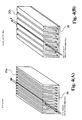
- FIGS. 4(A), 4(B) are diagrams illustrating two fin shapes, wherein FIG. 4(A) is a perspective view showing blade fins, and FIG. 4(B) is a perspective view showing corrugated fins.
- FIG. 5 is a diagram showing one example of a power converter circuit configured as the semiconductor module.
- FIGS. 6(A), 6(B) are diagrams illustrating a heretofore known semiconductor module as a first comparison example, wherein FIG. 6(A) is a perspective view showing an example of disposition of circuit elements, and FIG. 6(B) is a perspective view showing a main portion configuration of a water jacket of the cooler.
- FIGS. 7(A), 7(B) are perspective views showing, as second and third comparison examples, shapes of water jackets of types different from that of the cooler in FIG. 6(B) .
- FIGS. 8(A), 8(B) are diagrams illustrating a heretofore known semiconductor module as a fourth comparison example, wherein FIG. 8(A) is a plan view showing a shape of a water jacket, and FIG. 8(B) is a fragmentary perspective view thereof.
- FIG. 9 showing cooling characteristics of the water jackets of FIGS. 6(B) to 8(A) , is a diagram showing for each type a refrigerant flow rate distribution per circuit board position.
- FIG. 10 is a diagram showing for each type a pressure loss difference between an inlet and an outlet when the refrigerant is caused to flow through the semiconductor modules of FIGS. 6(A) to 8(B) .
- FIG. 11 is a plan view showing a shape of a water jacket used in a semiconductor module cooler of the invention.
- FIG. 12 is an illustration showing dimensions for each type of a flow velocity adjustment plate of the semiconductor module cooler of FIG. 11 .
- FIG. 13 showing cooling characteristics of the water jacket of FIG. 11 , is a diagram showing for each type a refrigerant flow velocity distribution per circuit board position.
- FIGS. 14(A)-14(C) showing cooling characteristics of the water jacket of FIG. 11 , are diagrams showing for each type a temperature of heat generated at a steady operation time for each circuit element portion.
- FIG. 15 is a diagram showing for each type a pressure loss difference between the inlet and the outlet when the refrigerant is caused to flow through the semiconductor module of FIG. 11 .
- FIG. 16 is a plan view showing a shape of a water jacket used in another semiconductor module cooler of the invention.
- FIG. 17 is an illustration showing dimensions for each type of a flow velocity adjustment plate, and of flow path widths of an inlet and outlet, in the semiconductor module of FIG. 16 .
- FIGS. 18(A), 18(B) show cooling characteristics of the water jacket of FIG. 16 , wherein FIG. 18(A) is a diagram showing for each type a refrigerant flow velocity distribution per circuit board position, and FIG. 18(B) is a diagram showing for each type a pressure loss difference between at the inlet and at the outlet.
- FIG. 1 is an external perspective view showing one example of a semiconductor module of the invention
- FIGS. 2 and 3 are respectively an arrow sectional view showing along line L 1 -L 1 of the semiconductor module of FIG. 1 and a perspective view showing a main portion configuration of a water jacket of a cooler.
- the arrows in FIG. 3 indicate a direction in which a refrigerant flows.
- a semiconductor module 10 is configured of a cooler 2 and a plurality of circuit element portions 3 A to 3 C disposed on the cooler 2 .
- the cooler 2 is configured of a water jacket 2 A acting as a fin cover and a fin base 2 B in which a plurality of fins 2 C is implanted to act as a heat sink, wherein the plurality of fins 2 C is housed inside the water jacket 2 A.
- the side on which the fin base 2 B is mounted in FIG. 2 is taken to be an “upper side”
- the arrow view direction with the upper side of the water jacket 2 A upward in FIG. 3 is taken to be a “front side”
- the side on which a refrigerant inlet portion 21 a and outlet portion 22 a are formed is taken to be a “left side”
- the side near an inlet 24 is taken to be an “upstream side”.
- the external shape of the water jacket 2 a of the cooler 2 is a substantially rectangular parallelepiped shape.
- the upper side principal surface of the cooler 2 is provided with a refrigerant inlet flow path 21 , the inlet portion 21 a , a refrigerant outlet flow path 22 , the outlet portion 22 a , and cooling flow paths 23 in which the fins 2 C are disposed.
- the inlet 24 for feeding the refrigerant into the interior and an outlet 25 for discharging the refrigerant to the exterior are provided in a left sidewall 2 Ab of the water jacket 2 A.
- the refrigerant inlet flow path 21 and the like are defined by a front sidewall 2 Aa, the left sidewall 2 Ab, a rear sidewall 2 Ac, a right sidewall 2 Ad, and a bottom wall 2 Ae.
- the fins 2 C are illustrated in FIG. 3 , for simplification of description.
- the refrigerant inlet flow path 21 is extended, parallel to the front sidewall 2 Aa of the water jacket 2 A, from the inlet 24 via the inlet portion 21 a to the right sidewall 2 Ad.
- the refrigerant outlet flow path 22 is extended, parallel to the rear sidewall 2 Ac of the water jacket 2 A, from the right sidewall 2 Ad to the outlet portion 22 a .
- the refrigerant inlet flow path 21 and refrigerant outlet flow path 22 are provided linearly and substantially parallel to each other inside the water jacket 2 A.
- guide portions 21 Si and 22 So having an inclination of 60° or less are formed respectively in a terminating portion of the refrigerant inlet flow path 21 into which the refrigerant flows from the inlet 24 and in a beginning portion of the refrigerant outlet flow path 22 which discharges the refrigerant to the outlet 25 .
- the cooling flow paths 23 being disposed as a third flow path in an intermediate position between the refrigerant inlet flow path 21 and refrigerant outlet flow path 22 , are formed so as to provide communication between the refrigerant inlet flow path 21 and refrigerant outlet flow path 22 . That is, the cooling flow paths 23 extend in a direction perpendicular to the direction of extension of the refrigerant inlet flow path 21 and the direction of extension of the refrigerant outlet flow path 22 .
- the inner surfaces of the left sidewall 2 Ab and right sidewall 2 Ad, which define the boundary of the cooling flow paths 23 are formed perpendicular to the bottom surface of the cooling flow paths 23 and the inner surface of the rear sidewall 2 Ac.
- the heat sink formed of the plurality of fins 2 C implanted in a base material 26 is formed in the cooling flow paths 23 , and the refrigerant flows through each of flow paths defined by the fins 2 C. Further, the refrigerant fed in from the inlet 24 passes through the refrigerant inlet flow path 21 , cooling flow paths 23 , and refrigerant outlet flow path 22 , and is discharged from the outlet 25 .
- the heat sink the external shape of which is a substantially rectangular parallelepiped, is disposed in the cooling flow paths 23 so that the left-side side surface, rear-side side surface, and right-side side surface are parallel to the respective inner surfaces of the corresponding left sidewall 2 Ab, rear sidewall 2 Ac, and right sidewall 2 Ad.
- the water jacket 2 A having this kind of configuration can be formed using, for example, a metal material such as aluminium, an aluminium alloy, copper, or a copper alloy.
- a metal material such as aluminium, an aluminium alloy, copper, or a copper alloy.
- the heretofore described kinds of refrigerant inlet flow path 21 , refrigerant outlet flow path 22 , cooling flow path 23 , inlet 24 , and outlet 25 can be formed by, for example, die casting.
- a material containing a carbon filler can also be used for the water jacket 2 A.
- the water jacket 2 A having this kind of configuration is such that the surface side on which are formed the refrigerant inlet flow path 21 , refrigerant outlet flow path 22 , and plurality of cooling flow paths 23 is sealed with the fin base 2 B, except the refrigerant inlet 24 and outlet 25 , as shown in FIGS. 1 and 2 . Also, the base material 26 with the plurality of fins 2 C implanted therein is joined to the water jacket 2 A side of the fin base 2 B.
- FIGS. 4(A), 4(B) are diagrams illustrating two fin shapes, wherein FIG. 4(A) is a perspective view showing blade fins, and FIG. 4(B) is a perspective view showing corrugated fins.
- the fins 2 C of the cooler 2 can be formed as a plurality of blade fins 2 Ca wherein plate-like fins are arranged in parallel, as shown in, for example, FIG. 4(A) .
- the blade fins 2 Ca are disposed in the cooling flow paths 23 , and the refrigerant circulates in a direction shown by the arrows in FIG. 4(A) .
- these kinds of blade fin 2 Ca are held by the base material 26 and fin base 2 B in the cooling flow paths 23 .
- the blade fins 2 Ca are illustrated in FIG. 4(A) , but it is also possible to use corrugated fins 2 Cb shown in FIG. 4(B) .
- fin 2 C having the shape of the blade fins 2 Ca or corrugated fins 2 Cb are integrated with the fin base 2 B and disposed with the fin 2 C side turned to face the water jacket 2 A, as shown in, for example, FIG. 2 .
- the fins 2 C are formed to a dimension (a height) such that a certain clearance C exists between the leading ends of the fins 2 C and the bottom wall 2 Ae of the water jacket 2 A.
- the base material 26 is configured integrally with the fin base 2 B, and when the fin base 2 B is disposed with the fin 2 C side thereof turned to face the water jacket 2 A, the fins 2 C are disposed in the cooling flow paths 23 of the water jacket 2 A. It is also possible to form the fins 2 C integrally with the fin base 2 B itself by die casting, brazing, any kind of welding, or the like, or after forming the fins 2 C in a convex shape from the fin base 2 B by die casting or pressing, to process the convex-shaped fins 2 C into a desired fin shape by a cutting or wire cutting method.
- the fins 2 C As this kind of fin shape of the fins 2 C, it is possible to use various heretofore known shapes. As the fins 2 C are resistant to the refrigerant flowing through the cooling flow paths 23 , it is desirable that the fins 2 C are of a low pressure loss to the refrigerant. Also, it is preferable that the shape and dimension of the fins 2 C are appropriately set taking into consideration conditions for feeding the refrigerant into the cooler 2 (that is, pump performance and the like), types of refrigerant (viscosity and the like), an intended amount of heat removal, and the like.
- the external shape of the heat sink formed of the fins 2 C are an approximate rectangular parallelepiped, preferably, a rectangular parallelepiped, or may be a shape wherein the rectangular parallelepiped is chamfered or modified as long as it does not impair the advantageous effects of the invention.
- the fins 2 C and fin base 2 B can be formed using, for example, a metal material such as aluminium, an aluminium alloy, copper, or a copper alloy, in the same way as the water jacket 2 A.
- the fins 2 C can be formed by, for example, joining predetermined pins or plate bodies formed using a metal material to a metal base material 26 , apart from the heretofore described blade fins 2 Ca and corrugated fins 2 Cb or the like.
- the base material 26 with the fins 2 C implanted therein in this way are joined to a predetermined region of the fin base 2 B of a metal plate or the like, that is, a region corresponding to the cooling flow paths 23 shown in FIG. 2 . It is not only that the base material 26 with the fins 2 C implanted therein in advance are joined to the fin base 2 B in this way, but it is also possible to configure the heat sink by joining the plurality of fins 2 C directly to the fin base 2 B.
- a pump provided on the upstream side of the cooler 2 is connected to, for example, the inlet 24 , and the outlet 25 is connected to a heat exchanger provided on the downstream side of the cooler 2 , thus configuring a closed loop refrigerant flow path including the cooler 2 , pump, and heat exchanger.
- the refrigerant is forcedly circulated in this kind of closed loop by the pump.
- Each circuit element portion 3 A to 3 C has a configuration wherein a total of four semiconductor devices, two for each of two types 32 and 33 , are mounted on a board 31 , as shown in, for example, FIG. 2 .
- the board 31 is configured so that conductor patterns 31 b and 31 c are formed one on each surface of an insulating substrate 31 a , as shown in, for example, FIG. 2 .
- a ceramic substrate of aluminium nitride or aluminium oxide can be used as the insulating substrate 31 a of the board 31 .
- the conductor patterns 31 b and 31 c on the insulating substrate 31 a can be formed using a metal (for example, a copper foil) such as copper or aluminium.
- the semi conductor devices 32 and 33 are joined to the conductor pattern 31 b side of the board 31 using their respective joining layers 34 of solder or the like, and electrically connected to the same conductor pattern 31 b directly or via their respective wires (not shown).
- the board 31 with the semiconductor devices 32 and 33 mounted thereon are joined to the fin base 2 B of the cooler 2 , via a joining layer 35 , on the other conductor pattern 31 c side.
- a protection layer for protecting the exposed and wire surfaces against contamination, corrosion, external force, or the like, may be formed on exposed surfaces of the conductor patterns 31 b and 31 c , and wire surfaces which electrically connect the semiconductor devices 32 and 33 and conductor pattern 31 b , by nickel plating or the like.
- FIG. 5 is a diagram showing one example of a power converter circuit configured as the semiconductor module.
- a free wheeling diode FWD
- an insulated gate bipolar transistor IGBT
- an inverter circuit 40 of, for example, three circuit element portions 3 A to 3 C.
- FIG. 5 illustrates the inverter circuit 40 which converts direct current into alternating current and supplies it to a three-phase alternating current motor 41 .
- the inverter circuit 40 includes a bridge circuit of the semiconductor device 33 , which is the IGBT, and the semiconductor device 32 , which is the FWD, for each of three phases, a U phase, V phase, and a W phase.
- the inverter circuit 40 by carrying out a switching control of the semiconductor device 33 , can convert direct current into alternating current and drive the three-phase alternating current motor 41 .
- circuit element portions 3 A to 3 C having the heretofore described kind of configuration are disposed on the fin base 2 B of the cooler 2 .
- the circuit element portions 3 A to 3 C can be connected so as to configure the inverter circuit, for example, on the cooler 2 .
- the above description has illustrated a case in which the number of circuit element portions 3 A to 3 C of the semiconductor module 10 is taken to be three.
- the number of circuit element portions is not necessarily limited to three, as in semiconductor modules to be shown next in FIGS. 6(A), 6(B) and the like as comparison examples.
- FIGS. 6(A), 6(B) are diagrams illustrating a heretofore known semiconductor module as a first comparison example, wherein FIG. 6(A) is a perspective view showing an example of disposition of circuit elements, and FIG. 6(B) is a perspective view showing a main portion configuration of a water jacket (type A) of the cooler.
- circuit element portions 3 D to 3 I, 3 Iu, and 3 Id are disposed in seven columns (B 1 to B 7 ) in the longer direction of the cooler 2 and in two rows in the short direction.
- the circuit element portions 3 D to 3 I, 3 Iu, and 3 Id by being appropriately combined, can be connected so as to configure the kind of plurality of inverter circuits 40 shown in, for example, FIG. 5 .
- the refrigerant inlet flow path 21 , the refrigerant outlet flow path 22 , and the cooling flow paths 23 in the rectangular region shown by the broken line are provided on one principal surface side, and of these, the cooling flow paths 23 are formed to a size corresponding to the fins 2 C.
- the fins 2 C are integrated with the fin base 2 B, and the fin 2 C side is disposed turned to face the water jacket 2 A, as shown in, for example, FIG. 2 . Further, the fin base 2 B integrated with the fins 2 C are eventually disposed inside the water jacket 2 A, as shown in FIGS. 1 and 2 .
- the cooler 2 including the water jacket 2 A, fin base 2 B, and fins 2 C can be configured.
- the guide portions 21 Si and 22 So having an inclination of 60° or less are formed respectively in the terminating portion of the refrigerant inlet flow path 21 into which the refrigerant flows from the inlet 24 and in the beginning portion of the refrigerant outlet flow path 22 which causes the refrigerant to flow out to the outlet 25 .
- the guide portion 21 Si has a uniform inclined surface all over a region opposite to the cooling flow paths 23 .
- FIGS. 7(A), 7(B) are perspective views showing, as second and third comparison examples, shapes of water jackets of types different from that of the cooler in FIG. 6(B) .
- FIG. 6(B) shows the type A wherein the inlet 24 and outlet 25 are disposed on the same surface side of the left sidewall 2 Ab.
- types with a plurality of shapes are used, such as a type B shown in FIG. 7(A) wherein the inlet 24 and outlet 25 are disposed in respective extreme opposite positions on the corresponding mutually opposing left and right sidewalls 2 Ab and 2 Ad, or a type C shown in FIG. 7(B) wherein the inlet 24 and outlet 25 are disposed in only the right sidewall 2 Ad. Because of this, with the water jackets 2 A to be actually used, it is necessary to optimize the shape of the refrigerant flow paths for each of the shapes of the water jackets 2 A.
- FIGS. 8(A), 8(B) are diagrams illustrating a heretofore known semiconductor module as a fourth comparison example, wherein FIG. 8(A) is a plan view showing a shape of a water jacket, and FIG. 8(B) is a fragmentary perspective view thereof.
- FIG. 8(A) shows a water jacket of an improvement example (a type D) wherein, in the water jacket of type A shown in FIG. 6(B) , as well as the width of the inlet 24 thereof being changed, a separation wall 27 is installed in the refrigerant inlet flow path 21 .
- a section of the inlet portion 21 a which feeds the refrigerant into the refrigerant inlet flow path 21 is formed in a tapered shape, and the flow path width of the inlet portion 21 a is changed so that a flow path width w 2 of the beginning portion of the refrigerant inlet flow path 21 is smaller than a flow path width w 1 of the inlet 24 .
- the water jacket 2 A of type D is such that the guide portion 21 Si having a 13 mm long inclined portion and a 5 mm long flat portion is disposed in the terminating portion of the refrigerant inlet flow path 21 .
- the separation wall 27 is formed in the refrigerant inlet flow path 21 so as to divide the flow path into two from the beginning portion.
- the separation wall 27 is disposed parallel to a refrigerant inflow-side side surface of the fins 2 C in the cooling flow paths 23 .
- the separation wall 27 disposed in the refrigerant inlet flow path 21 having an overall length of 215 mm in the refrigerant inlet flow path 21 , is provided so as to divide the flow path formed to a width of 10 mm into two flow paths, one with a width of 3.5 mm on the fin 2 C side and the other with a width of 5 mm on the front sidewall 2 Aa side.
- An upstream side leading end portion 27 a of the separation wall 27 is positioned at a boundary portion between the refrigerant inlet flow path 21 and inlet portion 21 a.
- the separation wall 27 By forming the separation wall 27 in this way, it is possible not only to increase the flow velocity of the refrigerant flowing in from the inlet 24 , but to increase the flow rate of the refrigerant flowing into the fins 2 C opposite to the leading end portion 27 a of the separation wall 27 . Because of this, the flow velocity of the refrigerant heading toward the terminating portion in the refrigerant inlet flow path 21 increases, and it is also possible to enhance the effect of cooling the circuit element portions 3 D (refer to FIG. 6(A) ) disposed in the position of the leading end portion 27 a of the separation wall 27 .
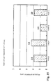
- FIG. 9 showing cooling characteristics of the water jackets of FIGS. 6(B) to 8(A)
- FIG. 10 is a diagram showing for each type a pressure loss difference between at the inlet and at the outlet when the refrigerant is caused to flow through the semiconductor module of each FIGS. 6(B) to 8(A) .
- the graphs of FIG. 9 each show, for each circuit board position (B 1 to B 7 ), the flow velocity of the refrigerant flowing between the blade fins 2 Ca when the blade fins 2 Ca shown in FIG. 4(A) as one example are disposed in the cooling flow paths 23 , and a refrigerant with a flow rate of 10 L/min is caused to flow from the inlet 24 .
- the water jacket 2 A of each type has urged flow characteristics wherein the flow velocity distribution of the refrigerant flowing to the circuit board positions B 1 to B 7 for each of the flow path shapes of the water jackets 2 A is uneven.
- the refrigerant flow velocity is high on the B 1 or B 7 side on which a pipe is connected, 0.15 m/s or more on both sides.
- the refrigerant flow rate is highest (0.10 m/s) in the circuit board position B 7 on the outlet 25 side.
- the refrigerant in the cooling flow paths 23 has biased flow characteristics wherein the flow velocity on the outlet 25 side, of parallel flow paths formed by the blade fins 2 Ca between the refrigerant inlet flow path 21 and refrigerant outlet flow path 22 , is significantly high. Also, with the type D improved on the type A, it can be seen that it is not only that the refrigerant flow velocity on the inlet 24 side is also improved, but it is possible to form a flow velocity distribution (biased flow characteristics) similar to that (those) of the type B wherein the inlet 24 and outlet 25 are disposed in the diagonally opposite positions.
- the pressure loss difference graphs shown in FIG. 10 show substantially the same pressure loss difference (3.2 to 3.4 kPa) in the water jackets 2 A of types A to C before being improved. As opposed to this, with the water jacket 2 A of type D wherein the width of the refrigerant inlet flow path 21 is reduced to 2 ⁇ 3, and the separation wall 27 is disposed therein, the pressure loss difference increases by 30% to 5.2 kPa.
- a differently configured one can be disposed in the seventh column on the cooler 2 , as the two circuit element portions 3 Iu and 3 Id, apart from the two rows and six columns of 12 circuit element portions 3 D to 3 I.
- the 12 circuit element portions 3 D to 3 I by being appropriately combined, can be connected so as to configure the kind of plurality of inverter circuits 40 illustrated in, for example, FIG. 5 .
- the circuit element portions 3 Iu and 3 Id can be configured as, for example, a boost converter circuit using a predetermined number of IGBTs and FWDs.
- the circuit element portions 3 Iu and 3 Id of the boost converter circuit are connected to a battery and the heretofore described inverter circuits 40 , and the voltage of the battery is boosted by the circuit element portions 3 Iu and 3 Id. Further, it is possible to adopt a kind of circuit configuration wherein the boosted direct current is converted into alternating current by the inverter circuits 40 and supplied to the three-phase alternating current motor 41 . In order to newly add circuit element portions 3 Iu and 3 Id different in type from these kinds of circuit element portion 3 D to 3 I, it is comparatively easy to dispose the circuit element portions 3 Iu and 3 Id in an end portion of the semiconductor module 10 A, as shown in FIG. 6(A) , when taking into consideration a wiring layout or the like in circuit design or manufacturing.
- the semiconductor module 10 A is such that two heat generation portions exist inside the fins 2 C in a direction of circulation of the refrigerant flowing through the cooling flow paths 23 of the cooler 2 . That is, the two heat generation portions are positioned separated into the upstream side and downstream side in a direction in which the refrigerant flows. Consequently, the refrigerant flowing on the downstream side reaches the downstream side heat generation portion with the temperature thereof already raised by heat absorption in the upstream side heat generation portion. Because of this, the efficiency of cooling the circuit element portions disposed on the upstream side becomes higher than that on the downstream side. When considering this kind of difference in cooling efficiency, ones of the circuit element portions 3 D to 3 I, with a larger amount of heat generated when they are driven, are disposed on the refrigerant inlet flow path 21 side, thereby enabling easier cooling.
- the flow velocity distribution of the refrigerant flowing through the cooling flow paths 23 of the cooler 2 has the heretofore described kinds of biased flow characteristic wherein the refrigerant flow velocity increases more in a position close to the outlet 25 than on the inlet 24 side.
- the cooling efficiency of the fins 2 C becomes higher in a high flow velocity portion in which the refrigerant flows quickly through the cooling flow paths 23 . Consequently, it is required that the refrigerant is circulated through the cooling flow paths 23 of the semiconductor module 10 A at a certain flow velocity or more in accordance with the amount of heat generated in the circuit element portions 3 D to 3 I, 3 Iu, and 3 Id.
- thermofluid analyses including physical phenomena such as a refrigerant flow, heat conduction, and heat transfer are necessary in order to simulate the flow path characteristics of the cooling flow paths 23 of this kind of semiconductor module 10 A. Also, when calculating an increase in the temperature of the refrigerant due to heat generation in the circuit element portions 3 D to 3 I, 3 Iu, and 3 Id, it is possible to obtain results of the analyses by giving a pressure loss incurred in a steady operation condition.
- the cooling performance is also of an uneven distribution in the same way.
- a change in cooling performance is more obtuse than a flow velocity fluctuation on the outlet 25 side on which the flow velocity is high, while a change in cooling performance is greater on the inlet 24 side on which the flow velocity is likely to be low. This means that a flow velocity component for which it is difficult to contribute to an improvement in cooling performance occurs on the outlet 25 side.
- the biased flow characteristics of the refrigerant are a phenomenon occurring in parallel flow paths in the cooling flow paths 23 sandwiched between the refrigerant inlet flow path 21 and refrigerant outlet flow path 22 .
- the intervals between the cooling fins 2 C disposed in the cooling flow paths 23 are increased, resistance against the refrigerant flowing from the refrigerant inlet flow path 21 to the fins 2 C decreases, and it becomes easier for the refrigerant to flow into the cooling flow paths 23 . Consequently, the fins 2 C in the cooling flow paths 23 are such that the wider the intervals therebetween they have a shape with, the more the biased flow characteristics are extended.
- Each following embodiment describes a semiconductor module cooler improved so as to adjust the flow velocity distribution of a semiconductor module with the inlet 24 and outlet 25 disposed on the same surface side, as in the heretofore known water jacket 2 A of type A shown in FIG. 6(B) .
- the cooling efficiencies of the semiconductor module coolers are all based on the flow velocity distribution verified by the heretofore described simulation on the premise of the nature (refrigerant properties) and cooling performance of the refrigerant itself.
- a flow velocity adjustment plate 28 is disposed in a boundary position between the refrigerant outlet flow path 22 and cooling flow paths 23 in order to adjust a biased flow in the semiconductor module.
- FIG. 11 is a plan view showing a shape of a water jacket used in the semiconductor module cooler of the invention.
- a water jacket 2 A of type Fc shown here is used as the cooler 2 of the semiconductor module 10 A in FIG. 6(A) . Consequently, in the water jacket 2 A of type Fc, the inlet 24 and outlet 25 are disposed in the left sidewall 2 Ab, in the same way as in the heretofore known type A shown in FIG. 6(B) .
- the inlet portion 21 a which feeds the refrigerant into the refrigerant inlet flow path 21 from the inlet 24 and the outlet portion 22 a for causing the refrigerant to flow out from the refrigerant outlet flow path 22 to the outlet 25 are formed so as to be long compared with those shown in FIG. 6(B) or FIG. 3 . That is, the inlet portion 21 a and outlet portion 22 a are both formed so as to protrude from the same left sidewall 2 Ab.
- the refrigerant inlet flow path 21 being 255.2 mm in length x, has in the terminating portion thereof the guide portion 21 Si with an approximately 45° inclined surface formed on the inner surface side of the front sidewall 2 Aa opposite to the front-side side surface (refrigerant inflow surface) of the fins 2 C disposed in the cooling flow paths 23 .
- a clearance y between the guide portion 21 Si in the terminating portion of the refrigerant inlet flow path 21 and the fins 2 C is 2 mm, as in the water jacket 2 A of type D ( FIG. 8(A) ).
- the flow velocity adjustment plate 28 is disposed in the boundary position between the refrigerant outlet flow path 22 and cooling flow paths 23 .
- the sidewall surface of the flow velocity adjustment plate 28 being formed parallel to the side surface of the fins 2 C, it is possible to reduce the rate of an increase in pressure loss due to a decrease in flow path sectional area, and furthermore, by increasing the flow path width of the refrigerant outlet flow path 22 , it is possible to obtain an excellent advantageous effect.
- FIG. 12 is an illustration showing dimensions for each type of the flow velocity adjustment plate in the semiconductor module cooler of FIG. 11 .
- water jackets 2 A of type E, type Ea, type Eb, type F, type Fa, and type Fb other than the water jacket 2 A of type Fc shown in FIG. 11 .
- the water jacket 2 A of any type is formed to a size such that the flow path widths (w 1 and w 2 ) of the refrigerant inlet flow path 21 and refrigerant outlet flow path 22 are both 15 mm equal to each other, the width of the cooling flow paths 23 is 255 mm, the length thereof is 117 mm, the clearance y between the guide portion 21 Si and fins 2 C is 2 mm, and the clearance y 2 between the flow velocity adjustment plate 28 and fins 2 C is 2 mm.
- the water jackets 2 A of type E, type Ea, and type Eb are the same as each other in that L and x 2 are 175 mm and 0 mm respectively, but differ from each other in that the height h of the flow velocity adjustment plate 28 varies within a range of from 9.5 mm to 5.5 mm.
- x 2 is set to 0 mm, and the height h of the flow velocity adjustment plate 28 is varied within a range of from 9.5 mm to 5.5 mm, but the types F, Fa, and Fb differ from each other in that the flow velocity adjustment plate 28 is formed with the length L thereof set to 215 mm so as to be longer than those of the type E series. Only the type Fc shown in FIG. 11 is different from all the other in that x 2 is set to 5 mm rather than 0 mm.
- FIG. 13 showing cooling characteristics of the water jackets of FIG. 11 , is a diagram showing for each type a refrigerant flow velocity distribution per circuit board position.
- Each flow velocity distribution shown in FIG. 13 is a result of simulating the refrigerant flow velocity between the fins 2 C disposed immediately below the central portion of the board of each circuit element portion 3 D to 3 I, 3 Iu, and 3 Id disposed in seven columns (positions B 1 to B 7 ).
- the flow velocities are shown in the order of B 1 to B 7 from the inlet 24 side toward the terminating portion of the refrigerant inlet flow path 21 .
- the refrigerant inlet flow paths 21 used in simulating the flow velocity distributions are all set to have an overall length of 255 m and a height of 10.5 mm.
- the flow velocity of the refrigerant discharged from the fins 2 C decreases due to pressure generated when the refrigerant smashes against the flow velocity adjustment plate 28 , meaning that it is possible to adjust the flow velocity distribution.
- this shows that it is possible to create an optional flow velocity distribution using the flow velocity adjustment plate 28 in the refrigerant outlet flow path 22 , and that even a slight clearance in the order of 5 mm has a great effect on a flow velocity adjustment in the vicinity of the outlet 25 of the refrigerant outlet flow path 22 .
- FIGS. 14(A)-14(C) showing cooling characteristics of the water jackets shown in FIG. 11 , are diagrams showing for each type a temperature of heat generated at a steady operation time for each circuit element portion.
- FIGS. 14(A)-14(C) are examples of simulation results obtained by the previously described method.
- a pressure loss incurred by the refrigerant in the water jacket 2 A when cooling the circuit element portions 3 D and the like differs for each type shown in FIG. 12 .
- heat losses in the water jackets 2 A are classified into two groups with three columns each from the inlet 24 side, the positions B 1 to B 3 of the circuit element portions 3 D to 3 F and the positions B 4 to B 6 of the circuit element portions 3 G to 3 I, as shown in FIG. 6(A) heretofore described, and can be set to the same size in the same group.
- heat losses different between in the upstream side circuit element portion 3 Id and in the downstream side circuit element portion 3 Iu are set in the circuit element portions 3 Iu and 3 Id in the seventh column.
- IGBT elements disposed one in each of the downstream side circuit element portion 3 D in the first column (position B 1 ) and circuit element portion 3 G in the fourth column (position B 4 ) are taken to be targets for comparison in generated heat temperature in FIGS. 14(A)-14(C) .
- one ( 3 Id), of the circuit element portions 3 Iu and 3 Id, with a greater incurred loss is taken to be a target for comparison.
- incurred loss values set one for each of the circuit element portions 3 D to 3 I, 3 Iu, and 3 Id in accordance with their respective generated heat amounts are set to a relationship of 3 D ⁇ 3 G ⁇ 3 Iu ⁇ 3 Id based on the relationship between the refrigerant flow velocity and the refrigerant temperature and cooling performance.
- the junction temperature (Tj) of the circuit element portion 3 Id is 136.7° C. in the type E, 134.7° C. in the type F, and 142.0° C. in the type Fb with the flow velocity distribution biased toward the outlet 25 side.
- the effect of a decrease in temperature by 5° C. or more can be seen depending on the length of the flow velocity adjustment plate 28 .
- the junction temperature of each IGBT changes along with a change in flow velocity distribution on the downstream side in the B 1 column and the downstream side in the B 4 column.
- FIG. 15 is a diagram showing for each type a pressure loss difference between at the inlet and at the outlet when the refrigerant is caused to flow into the semiconductor module of FIG. 11 .
- all the differences show a value less than 4.5 kPa. This shows that the pressure losses are low, and moreover, the flow velocities roughly coincide with each other, even when compared with the improvement example (type D) on the refrigerant inlet flow path 21 side, as in the fourth comparison example shown in FIG. 8(A) .
- the flow velocity adjustment plate 28 which carries out a flow adjustment on the refrigerant outlet flow path 22 side in this way, it is possible to reduce the pressure loss, and thus possible to reduce a load on a pump.
- the refrigerant inlet flow path 21 is defined by the inner surface of the bottom wall 2 Ae of the water jacket 2 A and the front-side side surface of the fins 2 C configuring the heat sink
- the refrigerant outlet flow path 22 is defined by the inner surface of the bottom wall 2 Ae and the rear-side side surface of the fins 2 C.
- a biased flow occurring in the refrigerant flow velocity in the fins 2 C can be resolved in such a way that the flow velocity adjustment plate 28 is disposed in the refrigerant outlet flow path 22 , and the flow velocity of the refrigerant flowing into the fins 2 C from the refrigerant inlet flow path 21 is appropriately adjusted by pressure generated when the refrigerant flowing out from the fins 2 C collides against the flow velocity adjustment plate 28 .
- the flow velocity adjustment plate 28 is disposed in the refrigerant outlet flow path 22 , and the flow velocity of the refrigerant flowing into the fins 2 C from the refrigerant inlet flow path 21 is appropriately adjusted by pressure generated when the refrigerant flowing out from the fins 2 C collides against the flow velocity adjustment plate 28 .
- the inlet 24 and outlet 25 are disposed in the same surface of the water jacket 2 A, and it is possible to configure a flow path shape so as to obtain cooling performance corresponding to the loss incurred in each different circuit element portion 3 D to 3 I, 3 Iu, and 3 Id. Above all, it is possible to inexpensively and easily manufacture the water jacket 2 A wherein the length from the inlet 24 to the outlet 25 is shorter.
- the fins 2 C configuring the heat sink, the front-side side surface of which is substantially parallel to an inflow direction of the refrigerant flowing in from the inlet 24 , are disposed in a position flush with the inner wall of the inlet portion 21 a so as not to block the flow of the refrigerant in the refrigerant inlet flow path 21 . Also, the interval from the bottom wall 2 Ae of the water jacket 2 A to the fin base 2 B, which defines the height of the refrigerant inlet flow path 21 , is constant.
- FIG. 16 is a plan view showing a shape of a water jacket used in another semiconductor module cooler of the invention.
- the inlet portion 21 a which feeds the refrigerant into the refrigerant inlet flow path 21 from the inlet 24 and the outlet portion 22 a for causing the refrigerant to flow out from the refrigerant outlet flow path 22 to the outlet 25 are formed protruding from the same left sidewall 2 Ab of the water jacket 2 A, in the same way as in the type D shown in FIG. 8(A) , the type Fc shown in FIG. 11 , and the like.
- the water jacket 2 A of type G is such that it is not only that the inlet 24 and outlet 25 of the cooler are formed on the same surface side, but the flow velocity adjustment plate 28 whose length is equal to the length x of the refrigerant outlet flow path 22 is disposed in the boundary position between the refrigerant outlet flow path 22 and cooling flow paths 23 .
- FIG. 17 is an illustration showing dimensions for each type of the flow velocity adjustment plate, and of the flow path widths of the inlet and outlet, in the semiconductor module cooler of FIG. 16 .
- the flow velocity adjustment plate 28 is formed in the refrigerant outlet flow path 22 of the type C so as to have an optional height not exceeding 8 mm vertically from the bottom wall 2 Ae surface of the water jacket 2 A.
- the cooling flow paths 23 are configured between the 10 mm wide refrigerant inlet flow path 21 and 15 mm wide refrigerant outlet flow path 22 .
- the dimensions of a type Ga, type Gb, type Gc, type H, and type I are shown here, apart from those of the type G.
- the flow velocity of the refrigerant flowing through the cooling paths 23 takes on a flow velocity distribution depending on the position of the outlet 25 of the water jacket 2 A, as previously described.
- the flow velocity adjustment plate 28 with a length L of 255 mm and a width (thickness) of 3 mm is formed in the refrigerant outlet flow path 22 (that is, the clearance x 2 between the flow velocity adjustment plate 28 and the left sidewall 2 Ab of the water jacket 2 A is 0 mm), and the flow velocity of the refrigerant discharged from the fins 2 C is brought into uniformity and adjusted into a steady flow velocity distribution.
- the water jacket 2 A of type G differs from the type E series and type F series shown in FIG. 12 in that the length of the flow velocity adjustment plate 28 is set to be the same as the length x of the refrigerant outlet flow path 22 (that is, the width of the cooling flow paths 23 ), and the flow velocity adjustment plate 28 is connected to the left sidewall 2 Ab (the refrigerant outlet 25 side sidewall of the cooling flow paths 23 ) of the water jacket 2 A.
- FIGS. 18(A), 18(B) show cooling characteristics of the water jackets of FIG. 16 , wherein FIG. 18(A) is a diagram showing for each type a refrigerant flow velocity distribution per circuit board position, and FIG. 18(B) is a diagram showing for each type a pressure loss difference between at the inlet and at the outlet.
- the flow velocity distributions shown in FIG. 18(A) are simulated immediately below the central portions of the boards of the circuit element portions 3 D to 3 I, 3 Iu, and 3 Id disposed in the circuit board positions B 1 to B 7 shown in FIG. 6(A) , and the refrigerant flow velocity distributions are compared by type for each of the positions B 1 to B 7 .
- the pressure loss difference is a pressure difference between at the inlet 24 and at the outlet 25 .
- the difference between the maximum flow velocity and minimum flow velocity is smallest in a case (the type T) in which the difference between the flow path width W 1 of the refrigerant inlet flow path 21 and the flow path width W 2 of the refrigerant outlet flow path 22 is 2.5 mm.
- the type H wherein the flow path width W 1 is equal to the flow path width W 2 ( ⁇ 15 mm)
- the flow velocity is reversed in the circuit board positions B 1 and B 7 . That is, the uniformity in flow velocity distribution is best realized with the water jacket 2 A of type I with the flow path width W 1 of the refrigerant inlet flow path 21 set to 12.5 mm.
- the pressure difference is 5.2 kPa in the water jacket 2 A of type I, and a change in pressure loss depends on the width W 1 of the refrigerant inlet flow path 21 . This shows that the uniformity in refrigerant flow velocity distribution is in a trade-off relationship with the pressure loss difference.
- the narrower the clearance y 2 (set herein to 2 mm in any type) between the fins 2 C and flow velocity adjustment plate 28 the greater the effect of adjusting the flow velocity distribution into uniformity, but this leads to an increase in pressure loss in the water jacket 2 A.
- the maximum pressure difference is 6 kPa or less in the water jacket 2 A of any one of types G to Gc, type H, or type I, these maximum pressure differences are within a range of a pressure loss difference of 10 kPa or less supposed in the water jacket 2 A, and even with the heretofore known pump performance, no problem arises in causing a sufficient refrigerant flow rate to flow.
Applications Claiming Priority (3)
| Application Number | Priority Date | Filing Date | Title |
|---|---|---|---|
| JP2011224469 | 2011-10-12 | ||
| JP2011-224469 | 2011-10-12 | ||
| PCT/JP2012/072554 WO2013054615A1 (ja) | 2011-10-12 | 2012-09-05 | 半導体モジュール用冷却器及び半導体モジュール |
Publications (2)
| Publication Number | Publication Date |
|---|---|
| US20140252590A1 US20140252590A1 (en) | 2014-09-11 |
| US9293391B2 true US9293391B2 (en) | 2016-03-22 |
Family
ID=48081674
Family Applications (2)
| Application Number | Title | Priority Date | Filing Date |
|---|---|---|---|
| US14/351,033 Active US9293391B2 (en) | 2011-10-12 | 2012-09-05 | Semiconductor module cooler and semiconductor module |
| US14/347,153 Active US9245821B2 (en) | 2011-10-12 | 2012-10-12 | Cooling device for semiconductor module, and semiconductor module |
Family Applications After (1)
| Application Number | Title | Priority Date | Filing Date |
|---|---|---|---|
| US14/347,153 Active US9245821B2 (en) | 2011-10-12 | 2012-10-12 | Cooling device for semiconductor module, and semiconductor module |
Country Status (6)
| Country | Link |
|---|---|
| US (2) | US9293391B2 (zh) |
| EP (2) | EP2768017B1 (zh) |
| JP (2) | JP5900506B2 (zh) |
| KR (2) | KR101906645B1 (zh) |
| CN (2) | CN103890938B (zh) |
| WO (2) | WO2013054615A1 (zh) |
Cited By (1)
| Publication number | Priority date | Publication date | Assignee | Title |
|---|---|---|---|---|
| US9960100B2 (en) | 2014-03-20 | 2018-05-01 | Fuji Electric Co., Ltd | Cooler and semiconductor module using same |
Families Citing this family (42)
| Publication number | Priority date | Publication date | Assignee | Title |
|---|---|---|---|---|
| JP5343007B2 (ja) * | 2007-11-26 | 2013-11-13 | 株式会社豊田自動織機 | 液冷式冷却装置 |
| KR101906645B1 (ko) | 2011-10-12 | 2018-10-10 | 후지 덴키 가부시키가이샤 | 반도체 모듈용 냉각기 및 반도체 모듈 |
| EP2840604B1 (en) * | 2012-04-16 | 2017-07-19 | Fuji Electric Co., Ltd. | Semiconductor device and cooler for semiconductor device |
| WO2014020808A1 (ja) * | 2012-08-03 | 2014-02-06 | 富士電機株式会社 | 冷却構造体及び電力変換装置 |
| WO2014069174A1 (ja) * | 2012-10-29 | 2014-05-08 | 富士電機株式会社 | 半導体装置 |
| JP6086033B2 (ja) * | 2013-06-05 | 2017-03-01 | 株式会社豊田自動織機 | インバータ装置 |
| DE112014000898T5 (de) * | 2013-09-05 | 2015-11-26 | Fuji Electric Co., Ltd. | Leistungshalbleitermodul |
| JP6164304B2 (ja) * | 2013-11-28 | 2017-07-19 | 富士電機株式会社 | 半導体モジュール用冷却器の製造方法、半導体モジュール用冷却器、半導体モジュール及び電気駆動車両 |
| WO2015137009A1 (ja) * | 2014-03-14 | 2015-09-17 | 富士電機株式会社 | 冷却器および該冷却器を有する半導体装置 |
| JP6098760B2 (ja) * | 2014-05-20 | 2017-03-22 | 富士電機株式会社 | 半導体モジュール用冷却器及びその製造方法 |
| JP6316096B2 (ja) * | 2014-05-28 | 2018-04-25 | 昭和電工株式会社 | 液冷式冷却装置 |
| KR102291151B1 (ko) * | 2014-11-03 | 2021-08-19 | 현대모비스 주식회사 | 전력변환장치용 냉각유로모듈 및 이를 구비한 전력변화장치 |
| CN105841403A (zh) * | 2015-01-12 | 2016-08-10 | 杭州三花研究院有限公司 | 冷却装置 |
| CN104754921B (zh) * | 2015-03-06 | 2018-03-06 | 西安电子科技大学 | 热源面温度均匀的微通道散热器 |
| JP6477276B2 (ja) * | 2015-06-12 | 2019-03-06 | 富士通株式会社 | クーリングプレート及びクーリングプレートを備える情報処理装置 |
| WO2016203885A1 (ja) * | 2015-06-17 | 2016-12-22 | 富士電機株式会社 | パワー半導体モジュール及び冷却器 |
| KR101848151B1 (ko) * | 2016-09-06 | 2018-04-12 | 황의수 | 소형냉각장치 |
| KR101848152B1 (ko) * | 2016-09-06 | 2018-04-12 | 황의수 | 복수 열전소자용 소형냉각장치 |
| JP6868633B2 (ja) * | 2016-09-23 | 2021-05-12 | 住友精密工業株式会社 | 冷却装置 |
| US10136564B2 (en) * | 2016-09-30 | 2018-11-20 | Denso Corporation | Power converter |
| CN106535572A (zh) * | 2016-11-29 | 2017-03-22 | 洛阳新巨能高热技术有限公司 | 一种新型水冷散热器 |
| CN106793677A (zh) * | 2016-11-29 | 2017-05-31 | 洛阳新巨能高热技术有限公司 | 一种水冷散热器 |
| CN106535573A (zh) * | 2016-11-29 | 2017-03-22 | 洛阳新巨能高热技术有限公司 | 水冷散热器 |
| CN106714511A (zh) * | 2016-11-29 | 2017-05-24 | 洛阳新巨能高热技术有限公司 | 新型水冷散热器 |
| EP3454367B1 (en) * | 2016-12-20 | 2021-08-25 | Fuji Electric Co., Ltd. | Semiconductor module |
| JP6880776B2 (ja) * | 2017-01-27 | 2021-06-02 | 株式会社デンソー | 電力変換装置 |
| DE102018112601A1 (de) * | 2017-05-31 | 2018-12-06 | Hanon Systems | Elektroelement-Kühlungsmodul |
| JP6636996B2 (ja) * | 2017-07-11 | 2020-01-29 | ファナック株式会社 | Ldモジュール冷却装置及びレーザ装置 |
| US10292316B2 (en) * | 2017-09-08 | 2019-05-14 | Hamilton Sundstrand Corporation | Power module with integrated liquid cooling |
| JP7205071B2 (ja) | 2018-04-02 | 2023-01-17 | 富士電機株式会社 | 冷却装置、半導体モジュールおよび車両 |
| JP7124425B2 (ja) | 2018-05-02 | 2022-08-24 | 富士電機株式会社 | 冷却装置、半導体モジュールおよび車両 |
| DE102018112000A1 (de) * | 2018-05-18 | 2019-11-21 | Rogers Germany Gmbh | System zum Kühlen eines Metall-Keramik-Substrats, ein Metall-Keramik-Substrat und Verfahren zum Herstellen des Systems |
| JP7087850B2 (ja) * | 2018-09-05 | 2022-06-21 | 株式会社デンソー | 半導体装置 |
| DE102018215142A1 (de) * | 2018-09-06 | 2020-03-12 | Robert Bosch Gmbh | Sensoreinheit eines Fahrzeugs |
| US11129310B2 (en) * | 2018-11-22 | 2021-09-21 | Fuji Electric Co., Ltd. | Semiconductor module, vehicle and manufacturing method |
| DE112019006927B4 (de) | 2019-02-26 | 2022-12-29 | Mitsubishi Electric Corporation | Halbleitervorrichtung, Herstellungsverfahren für eine Halbleitervorrichtung sowie Leistungswandler |
| JP7367418B2 (ja) * | 2019-09-13 | 2023-10-24 | 富士電機株式会社 | 半導体モジュールおよび車両 |
| KR102328940B1 (ko) * | 2019-12-13 | 2021-11-19 | 한국전자기술연구원 | 핀휜 구조 히트싱크의 균일 냉각성을 향상시키기 위한 수냉각 장치 구조 |
| TWI738602B (zh) * | 2020-01-22 | 2021-09-01 | 訊凱國際股份有限公司 | 多通道薄熱交換器 |
| JP7229195B2 (ja) * | 2020-03-10 | 2023-02-27 | 三菱電機株式会社 | 発熱素子冷却装置 |
| CN111447805A (zh) * | 2020-05-11 | 2020-07-24 | 珠海格力电器股份有限公司 | 散热效率高的散热组件、电器盒及空调 |
| JP6961047B1 (ja) * | 2020-07-17 | 2021-11-05 | 三菱電機株式会社 | 電力変換装置 |
Citations (22)
| Publication number | Priority date | Publication date | Assignee | Title |
|---|---|---|---|---|
| US2934322A (en) | 1955-09-01 | 1960-04-26 | Frederick E Hazard | Heat exchanger |
| DE19514545A1 (de) | 1995-04-20 | 1996-10-24 | Daimler Benz Ag | Anordnung von mehreren mit elektronischen Bauelementen versehenen Mikrokühleinrichtungen |
| US5978220A (en) * | 1996-10-23 | 1999-11-02 | Asea Brown Boveri Ag | Liquid cooling device for a high-power semiconductor module |
| JP2001035981A (ja) | 1999-07-16 | 2001-02-09 | Toshiba Corp | 半導体素子用冷却器及びこれを用いた電力変換装置 |
| JP2001352025A (ja) | 2000-06-05 | 2001-12-21 | Toshiba Corp | 発熱体冷却装置 |
| JP2006080211A (ja) | 2004-09-08 | 2006-03-23 | Toyota Motor Corp | 半導体装置 |
| JP2006210819A (ja) | 2005-01-31 | 2006-08-10 | Toyota Motor Corp | 半導体冷却装置 |
| US20060225867A1 (en) * | 2005-04-11 | 2006-10-12 | Samsung Electronics Co., Ltd. | Heat sink apparatus for electronic device |
| JP2007012722A (ja) | 2005-06-28 | 2007-01-18 | Honda Motor Co Ltd | パワー半導体モジュール |
| JP2008205371A (ja) | 2007-02-22 | 2008-09-04 | Mitsubishi Materials Corp | 液冷式冷却器並びにパワー素子搭載用ユニット |
| US20080237847A1 (en) | 2007-03-30 | 2008-10-02 | Nichicon Corporation | Power semiconductor module, and power semiconductor device having the module mounted therein |
| JP2008263137A (ja) | 2007-04-13 | 2008-10-30 | Nippon Inter Electronics Corp | 冷却装置 |
| US20090178792A1 (en) | 2008-01-15 | 2009-07-16 | Kabushiki Kaisha Toyota Jidoshokki | Liquid-cooled-type cooling device |
| JP2009266936A (ja) | 2008-04-23 | 2009-11-12 | Denso Corp | 積層型冷却器 |
| US20090314474A1 (en) | 2005-04-27 | 2009-12-24 | Kabushiki Kaisha Toyota Jidoshokki | Heat sink for power module |
| US20100051234A1 (en) | 2008-08-26 | 2010-03-04 | Kabushiki Kaisha Toyota Jidoshokki | Liquid-cooled-type cooling device |
| US20100090336A1 (en) * | 2007-01-11 | 2010-04-15 | Toyota Jidosha Kabushiki Kaisha | Semiconductor element cooling structure |
| JP2010203694A (ja) | 2009-03-04 | 2010-09-16 | Showa Denko Kk | 液冷式冷却装置 |
| EP2234153A1 (en) | 2007-11-26 | 2010-09-29 | Kabushiki Kaisha Toyota Jidoshokki | Liquid-cooled cooling device |
| WO2011018882A1 (en) | 2009-08-10 | 2011-02-17 | Fuji Electric Systems Co., Ltd. | Semiconductor module and cooling unit |
| JP2011134979A (ja) | 2009-12-25 | 2011-07-07 | Fuji Electric Co Ltd | 液体冷却式ヒートシンク |
| WO2013054887A1 (ja) | 2011-10-12 | 2013-04-18 | 富士電機株式会社 | 半導体モジュール用冷却器及び半導体モジュール |
Family Cites Families (7)
| Publication number | Priority date | Publication date | Assignee | Title |
|---|---|---|---|---|
| DE19514544A1 (de) * | 1995-04-20 | 1996-10-24 | Daimler Benz Ag | Mikrokühleinrichtung |
| JP2000340727A (ja) * | 1999-05-26 | 2000-12-08 | Nissan Motor Co Ltd | 電子部品の冷却構造 |
| JP2007242724A (ja) * | 2006-03-06 | 2007-09-20 | Seiko Epson Corp | マイクロチャンネル構造体、マイクロチャンネル構造体の製造方法及び電子機器 |
| JP2008235725A (ja) * | 2007-03-23 | 2008-10-02 | Calsonic Kansei Corp | 水冷式ヒートシンク |
| JP5046378B2 (ja) | 2007-03-30 | 2012-10-10 | ニチコン株式会社 | パワー半導体モジュール、および該モジュールを搭載したパワー半導体デバイス |
| JP4845912B2 (ja) | 2008-03-25 | 2011-12-28 | 株式会社豊田自動織機 | 液冷式冷却装置 |
| JP5565459B2 (ja) | 2010-04-21 | 2014-08-06 | 富士電機株式会社 | 半導体モジュール及び冷却器 |
-
2012
- 2012-09-05 KR KR1020147009286A patent/KR101906645B1/ko active IP Right Grant
- 2012-09-05 US US14/351,033 patent/US9293391B2/en active Active
- 2012-09-05 JP JP2013538476A patent/JP5900506B2/ja active Active
- 2012-09-05 CN CN201280050253.9A patent/CN103890938B/zh active Active
- 2012-09-05 WO PCT/JP2012/072554 patent/WO2013054615A1/ja active Application Filing
- 2012-09-05 EP EP12839733.8A patent/EP2768017B1/en active Active
- 2012-10-12 KR KR1020147009296A patent/KR101906646B1/ko active IP Right Grant
- 2012-10-12 JP JP2013538590A patent/JP5900507B2/ja active Active
- 2012-10-12 EP EP12839889.8A patent/EP2768018B1/en active Active
- 2012-10-12 WO PCT/JP2012/076453 patent/WO2013054887A1/ja active Application Filing
- 2012-10-12 CN CN201280049849.7A patent/CN103858224B/zh active Active
- 2012-10-12 US US14/347,153 patent/US9245821B2/en active Active
Patent Citations (26)
| Publication number | Priority date | Publication date | Assignee | Title |
|---|---|---|---|---|
| US2934322A (en) | 1955-09-01 | 1960-04-26 | Frederick E Hazard | Heat exchanger |
| DE19514545A1 (de) | 1995-04-20 | 1996-10-24 | Daimler Benz Ag | Anordnung von mehreren mit elektronischen Bauelementen versehenen Mikrokühleinrichtungen |
| US5737186A (en) | 1995-04-20 | 1998-04-07 | Daimler-Benz Ag | Arrangement of plural micro-cooling devices with electronic components |
| US5978220A (en) * | 1996-10-23 | 1999-11-02 | Asea Brown Boveri Ag | Liquid cooling device for a high-power semiconductor module |
| JP2001035981A (ja) | 1999-07-16 | 2001-02-09 | Toshiba Corp | 半導体素子用冷却器及びこれを用いた電力変換装置 |
| JP2001352025A (ja) | 2000-06-05 | 2001-12-21 | Toshiba Corp | 発熱体冷却装置 |
| JP2006080211A (ja) | 2004-09-08 | 2006-03-23 | Toyota Motor Corp | 半導体装置 |
| JP2006210819A (ja) | 2005-01-31 | 2006-08-10 | Toyota Motor Corp | 半導体冷却装置 |
| US20060225867A1 (en) * | 2005-04-11 | 2006-10-12 | Samsung Electronics Co., Ltd. | Heat sink apparatus for electronic device |
| US20090314474A1 (en) | 2005-04-27 | 2009-12-24 | Kabushiki Kaisha Toyota Jidoshokki | Heat sink for power module |
| JP2007012722A (ja) | 2005-06-28 | 2007-01-18 | Honda Motor Co Ltd | パワー半導体モジュール |
| US20100090336A1 (en) * | 2007-01-11 | 2010-04-15 | Toyota Jidosha Kabushiki Kaisha | Semiconductor element cooling structure |
| JP2008205371A (ja) | 2007-02-22 | 2008-09-04 | Mitsubishi Materials Corp | 液冷式冷却器並びにパワー素子搭載用ユニット |
| US20080237847A1 (en) | 2007-03-30 | 2008-10-02 | Nichicon Corporation | Power semiconductor module, and power semiconductor device having the module mounted therein |
| JP2008263137A (ja) | 2007-04-13 | 2008-10-30 | Nippon Inter Electronics Corp | 冷却装置 |
| EP2234153A1 (en) | 2007-11-26 | 2010-09-29 | Kabushiki Kaisha Toyota Jidoshokki | Liquid-cooled cooling device |
| US20100252235A1 (en) | 2007-11-26 | 2010-10-07 | Kabushiki Kaisha Toyota Jidoshokki | Liquid-cooled-type cooling device |
| US20090178792A1 (en) | 2008-01-15 | 2009-07-16 | Kabushiki Kaisha Toyota Jidoshokki | Liquid-cooled-type cooling device |
| JP2009266936A (ja) | 2008-04-23 | 2009-11-12 | Denso Corp | 積層型冷却器 |
| US20100051234A1 (en) | 2008-08-26 | 2010-03-04 | Kabushiki Kaisha Toyota Jidoshokki | Liquid-cooled-type cooling device |
| JP2010203694A (ja) | 2009-03-04 | 2010-09-16 | Showa Denko Kk | 液冷式冷却装置 |
| WO2011018882A1 (en) | 2009-08-10 | 2011-02-17 | Fuji Electric Systems Co., Ltd. | Semiconductor module and cooling unit |
| US8933557B2 (en) | 2009-08-10 | 2015-01-13 | Fuji Electric Co., Ltd. | Semiconductor module and cooling unit |
| JP2011134979A (ja) | 2009-12-25 | 2011-07-07 | Fuji Electric Co Ltd | 液体冷却式ヒートシンク |
| WO2013054887A1 (ja) | 2011-10-12 | 2013-04-18 | 富士電機株式会社 | 半導体モジュール用冷却器及び半導体モジュール |
| US20140252590A1 (en) | 2011-10-12 | 2014-09-11 | Fuji Electric Co., Ltd. | Semiconductor module cooler and semiconductor module |
Non-Patent Citations (3)
| Title |
|---|
| Europe Patent Office, "Search Report for EP 12839889.8," Jun. 2, 2015. |
| Japan Patent Office, "Office Action for JP 2013-538476," Sep. 1, 2015. |
| PCT, "International Search Report for International Application No. PCT/JP2012/072554". |
Cited By (1)
| Publication number | Priority date | Publication date | Assignee | Title |
|---|---|---|---|---|
| US9960100B2 (en) | 2014-03-20 | 2018-05-01 | Fuji Electric Co., Ltd | Cooler and semiconductor module using same |
Also Published As
| Publication number | Publication date |
|---|---|
| KR101906646B1 (ko) | 2018-10-10 |
| EP2768018A4 (en) | 2015-07-01 |
| EP2768018B1 (en) | 2020-02-26 |
| CN103890938B (zh) | 2017-10-13 |
| JP5900506B2 (ja) | 2016-04-06 |
| WO2013054615A1 (ja) | 2013-04-18 |
| EP2768017A1 (en) | 2014-08-20 |
| KR20140088089A (ko) | 2014-07-09 |
| CN103858224A (zh) | 2014-06-11 |
| WO2013054887A1 (ja) | 2013-04-18 |
| EP2768017A4 (en) | 2015-07-01 |
| US20140239486A1 (en) | 2014-08-28 |
| KR20140070589A (ko) | 2014-06-10 |
| JP5900507B2 (ja) | 2016-04-06 |
| KR101906645B1 (ko) | 2018-10-10 |
| US20140252590A1 (en) | 2014-09-11 |
| JPWO2013054615A1 (ja) | 2015-03-30 |
| JPWO2013054887A1 (ja) | 2015-03-30 |
| EP2768017B1 (en) | 2019-10-23 |
| EP2768018A1 (en) | 2014-08-20 |
| CN103890938A (zh) | 2014-06-25 |
| CN103858224B (zh) | 2018-04-10 |
| US9245821B2 (en) | 2016-01-26 |
Similar Documents
| Publication | Publication Date | Title |
|---|---|---|
| US9293391B2 (en) | Semiconductor module cooler and semiconductor module | |
| US9237676B2 (en) | Semiconductor module cooler and semiconductor module | |
| US9220182B2 (en) | Semiconductor module cooler and semiconductor module | |
| CN101510534B (zh) | 用于功率半导体器件的冷却系统及包括该系统的功率模块 | |
| US8902589B2 (en) | Semiconductor module and cooler | |
| US8933557B2 (en) | Semiconductor module and cooling unit | |
| JP5381561B2 (ja) | 半導体冷却装置 | |
| US9502329B2 (en) | Semiconductor module cooler | |
| WO2013157467A1 (ja) | 半導体装置および半導体装置用冷却器 |
Legal Events
| Date | Code | Title | Description |
|---|---|---|---|
| AS | Assignment |
Owner name: FUJI ELECTRIC CO., LTD., JAPAN Free format text: ASSIGNMENT OF ASSIGNORS INTEREST;ASSIGNORS:GOHARA, HIROMICHI;MOROZUMI, AKIRA;ICHIMURA, TAKESHI;REEL/FRAME:032850/0024 Effective date: 20140423 |
|
| STCF | Information on status: patent grant |
Free format text: PATENTED CASE |
|
| CC | Certificate of correction | ||
| MAFP | Maintenance fee payment |
Free format text: PAYMENT OF MAINTENANCE FEE, 4TH YEAR, LARGE ENTITY (ORIGINAL EVENT CODE: M1551); ENTITY STATUS OF PATENT OWNER: LARGE ENTITY Year of fee payment: 4 |
|
| MAFP | Maintenance fee payment |
Free format text: PAYMENT OF MAINTENANCE FEE, 8TH YEAR, LARGE ENTITY (ORIGINAL EVENT CODE: M1552); ENTITY STATUS OF PATENT OWNER: LARGE ENTITY Year of fee payment: 8 |