US9293261B2 - Multilayer ceramic capacitor - Google Patents
Multilayer ceramic capacitor Download PDFInfo
- Publication number
- US9293261B2 US9293261B2 US14/033,189 US201314033189A US9293261B2 US 9293261 B2 US9293261 B2 US 9293261B2 US 201314033189 A US201314033189 A US 201314033189A US 9293261 B2 US9293261 B2 US 9293261B2
- Authority
- US
- United States
- Prior art keywords
- multilayer ceramic
- laminating direction
- ceramic capacitor
- samples
- internal electrode
- Prior art date
- Legal status (The legal status is an assumption and is not a legal conclusion. Google has not performed a legal analysis and makes no representation as to the accuracy of the status listed.)
- Active, expires
Links
Images


Classifications
-
- H—ELECTRICITY
- H01—ELECTRIC ELEMENTS
- H01G—CAPACITORS; CAPACITORS, RECTIFIERS, DETECTORS, SWITCHING DEVICES OR LIGHT-SENSITIVE DEVICES, OF THE ELECTROLYTIC TYPE
- H01G4/00—Fixed capacitors; Processes of their manufacture
- H01G4/30—Stacked capacitors
-
- H—ELECTRICITY
- H01—ELECTRIC ELEMENTS
- H01G—CAPACITORS; CAPACITORS, RECTIFIERS, DETECTORS, SWITCHING DEVICES OR LIGHT-SENSITIVE DEVICES, OF THE ELECTROLYTIC TYPE
- H01G4/00—Fixed capacitors; Processes of their manufacture
- H01G4/002—Details
- H01G4/018—Dielectrics
- H01G4/06—Solid dielectrics
- H01G4/08—Inorganic dielectrics
- H01G4/12—Ceramic dielectrics
-
- H—ELECTRICITY
- H01—ELECTRIC ELEMENTS
- H01G—CAPACITORS; CAPACITORS, RECTIFIERS, DETECTORS, SWITCHING DEVICES OR LIGHT-SENSITIVE DEVICES, OF THE ELECTROLYTIC TYPE
- H01G4/00—Fixed capacitors; Processes of their manufacture
- H01G4/002—Details
- H01G4/255—Means for correcting the capacitance value
Definitions
- the present invention relates to a multilayer ceramic capacitor comprising a capacitor body of a structure where multiple internal electrode layers are laminated via dielectric layers.
- the need for reducing the size and increasing the capacity of this type of multilayer ceramic capacitor is still high, and to satisfy this need, further thickness reduction of internal electrode layers and dielectric layers is inevitable.
- the CR product product of capacitance C and insulation resistance R
- the CR product is widely known as a value representing the characteristics of the multilayer ceramic capacitor, and generally the lower limit of CR product is set according to the nominal capacitance.
- Patent Literature 1 describes an invention that limits the grain size and volume ratio of the dielectric layer crystal contained in the dielectric layer whose thickness is 2.5 ⁇ m or less so as to prevent the CR product from dropping, but since accurately limiting the grain size and volume ratio of the dielectric layer crystal is difficult due to the limitations of the manufacturing method, drop in CR product may not be prevented as expected.
- Patent Literature 1 Japanese Patent Laid-open No. 2001-338828
- An object of the present invention is to provide a multilayer ceramic capacitor whose CR product can be prevented from dropping with certainty even when the dielectric layer becomes thinner, such as when its thickness becomes 1.0 ⁇ m or less, for example.
- the present invention provides a multilayer ceramic capacitor comprising a capacitor body of a structure where multiple internal electrode layers are laminated via dielectric layers, wherein, when the part constituted by two adjacent internal electrode layers in the laminating direction and one dielectric layer present between the two internal electrode layers is considered a unit capacitor, then the capacitances of multiple unit capacitors arranged in the laminating direction form a distribution that gradually increases from both sides in the laminating direction toward the inside, while gradually decreasing from the two apexes of increase toward the center in the laminating direction.
- the term “gradually” refers to continuously, steadily, progressively, incrementally, and/or without sudden changes.
- a multilayer ceramic capacitor is provided whose CR product can be inhibited from dropping with certainty even when the dielectric layer becomes thinner, such as when its thickness becomes 1.0 ⁇ m or less, for example.
- FIG. 1 is a longitudinal section view of a multilayer ceramic capacitor to which the present invention is applied;
- (B) in FIG. 1 is a lateral section view of the multilayer ceramic capacitor cut along line B-B in (A) in FIG. 1 ;
- (C) in FIG. 1 is a drawing showing an equivalent circuit of the multilayer ceramic capacitor;
- (D) in FIG. 1 is a drawing showing the capacitance distribution of the unit capacitor in the multilayer ceramic capacitor.
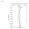
- FIG. 2 is a drawing showing the capacitance distribution of the unit capacitor in a sample corresponding to the multilayer ceramic capacitor in FIG. 1 .
- FIG. 3 is a table showing the specifications and characteristics of a sample corresponding to the multilayer ceramic capacitor in FIG. 1 .
- FIG. 1 to (D) in FIG. 1 are referenced to explain the structure of a multilayer ceramic capacitor 10 to which the present invention is applied, as well as the capacitance distribution of the unit capacitor in the multilayer ceramic capacitor 10 .
- the length represents the dimension in the lateral direction in (A) in FIG. 1
- width represents the dimension in the vertical direction in (B) in FIG. 1
- height represents the dimension in the vertical direction in (A) in FIG. 1 .
- the capacitor body 11 has a structure where a total of 20 internal electrode layers 12 are laminated via dielectric layers 13 (totaling 19), and a top protection part and bottom protection part (not denoted by symbols) are provided above the top internal electrode layer 12 and below the bottom internal electrode layer 12 , respectively, each protection part constituted only by multiple dielectric layers 13 laminated together. Additionally, since the width of each internal electrode layer 12 is smaller than the width of the dielectric layer 13 , a margin (not denoted by symbol) formed only by multiple dielectric layers 13 alone is present on one side and the other side of the capacitor body 11 in its width direction. Note that, although the number of internal electrode layers 12 is 20 in (A) in FIG. 1 and (B) in FIG. 1 for the purpose of illustrative convenience, the number of internal electrode layers constituting an actual multilayer ceramic capacitor meeting the need for size reduction and capacity increase can be as many as 100 or even more.
- Each internal electrode layer 12 is formed by nickel, copper, palladium, platinum, silver, gold, or alloy thereof, and the like, where each layer is made of the same material and has roughly the same thickness and shape (roughly rectangular).
- Each dielectric layer 13 including each dielectric layer 13 constituting the top protection part or bottom protection part, is formed by barium titanate, strontium titanate, calcium titanate, magnesium titanate, calcium zirconate, calcium zirconate titanate, barium zirconate, or titanium oxide, and the like, where each layer is made of the same material and has roughly the same thickness and shape (roughly rectangular), and each layer has a shape longer and wider than the shape of each internal electrode layer 12 .
- the odd-numbered internal electrode layers 12 (totaling 10) from the top and even-numbered internal electrode layers 12 (totaling 10) from the top in (A) in FIG. 1 are staggered in the length direction, where the ends of the odd-numbered internal electrode layers 12 from the top are electrically connected to the left external electrode 14 , while the ends of the even-numbered internal electrode layers 12 from the top are electrically connected to the right external electrode 14 .
- Each external electrode 14 has a double-layer structure constituted by a base layer (not denoted by symbol) contacting both ends of the capacitor body 11 in its length direction and a surface layer formed on the surface of the base layer, or a multi-layer structure having at least one intermediate layer between the base layer and surface layer.
- the base layer is formed by the same material as the internal electrode layer 12
- the surface layer is formed by tin, palladium, gold, zinc, etc.
- the intermediate layer is formed by platinum, palladium, gold, copper, nickel, etc.
- the multilayer ceramic capacitor 10 includes a total of 19 unit capacitors UC 1 to UC 19 arranged in the laminating direction and the unit capacitors UC 1 to UC 19 are connected in parallel to the pair of external electrodes 14 , as shown in (C) in FIG. 1 .
- the capacitances of the total of 19 unit capacitors UC 1 to UC 19 arranged in the laminating direction form a distribution of roughly a W shape that gradually increases from both sides in the laminating direction toward the inside, while gradually decreasing from the two apexes of increase toward the center in the laminating direction, as shown by the thick solid line in (D) in FIG. 1 .
- the capacitances of the unit capacitor UC 1 and UC 19 on both sides in the laminating direction are smaller than the capacitance of the unit capacitor UC 10 at the center in the laminating direction.
- each internal electrode layer 12 is formed by nickel and each dielectric layer 13 is formed by barium titanate is used as an example.
- a base slurry containing barium titanate powder, ethanol (solvent), polyvinyl butyral (binder), and dispersant and other additives is prepared, to provide a first dielectric layer slurry obtained by adding sintering suppressant to the base slurry and a second dielectric layer slurry obtained by adding sintering auxiliary to the base slurry.
- Rare earth oxide can be used for the sintering suppressant in the first dielectric layer slurry, for example, and silica or glass compound can be used for the sintering auxiliary in the second dielectric layer slurry, for example.
- a desired amount by which to add each of the above is 0.5 to 5.0 percent by weight, for example.
- an internal electrode layer paste containing nickel powder, terpineol (solvent), ethyl cellulose (binder), and dispersant and other additives is prepared.
- a die-coater, etc. is used to apply the first dielectric layer slurry onto a carrier film to the specified thickness and width, after which the film is dried to produce a first sheet (containing the sintering suppressant).
- a die-coater, etc. is used to apply the second dielectric layer slurry onto a carrier film to the specified thickness and width, after which the film is dried to produce a second sheet (containing the sintering auxiliary).
- a screen printer, etc. is used to apply the internal electrode layer paste onto the second sheet to the specified thickness and shape in a matrix or zigzag pattern, after which the sheet is dried to produce a third sheet on which internal electrode layer patterns are formed.
- a pickup head with stamping blade and heater, etc. is used to laminate and thermally bond a specified number of first unit sheets (containing the sintering suppressant) that have been stamped to the specified shape from the first sheet, after which a specified number of second unit sheets (containing the sintering auxiliary and having internal electrode layer patterns on them) that have been stamped to the specified shape from the third sheet are laminated and thermally bonded on top, after which a specified number of first unit sheets (containing the sintering suppressant) that have been stamped to the specified shape from the first sheet are laminated and thermally bonded on top, and the obtained laminate is finally thermally bonded using a hot hydrostatic press machine, etc., to produce a non-sintered laminated sheet.
- the non-sintered laminated sheet is cut to grid using a dicing machine, etc., to produce non-sintered chips, each corresponding to the capacitor body 11 .
- non-sintered chips are put in a sintering furnace and sintered (including binder removal and sintering) in a reducing ambience or ambience of low partial oxygen pressure based on a temperature profile appropriate for the nickel powder and barium titanate powder.
- An essential point of this sintering process is to raise the temperature quickly, such as at a rate of 5000 to 10000° C./hr, during sintering to actively cause the progress of sintering to drop from the surface of the non-sintered chip toward the center.
- a roller coater, etc. is used to apply an external electrode paste (the internal electrode layer paste is diverted for this purpose) on both ends of the sintered chip in its length direction and then the chip is baked in the same ambience as mentioned above to form a base layer, after which a surface layer, or an intermediate layer and surface layer, is/are formed by electroplating, etc., on the surface of the base layer to produce a pair of external electrodes.
- an external electrode paste the internal electrode layer paste is diverted for this purpose
- the samples 1a to 1g, 2a to 2g, and 3a to 3g are each a multilayer ceramic capacitor having a structure equivalent to that of the multilayer ceramic capacitor 10 , where the reference length and width dimensions of each sample are 1.0 mm and 0.5 mm, respectively, the number of internal electrode layers 12 is 100, and average thickness of the internal electrode layer 12 is 1.2 ⁇ m.
- the term “average” refers to an average of all the samples (or the entire areas) at issue, an average of randomly selected samples (or areas) at issue, an average of samples (or areas) representing all the samples (or the entire areas) at issue, or an average equivalent to the foregoing.
- the samples 1a to 1g, 2a to 2g, and 3a to 3g are such that the average thickness of the dielectric layer 13 is 1.0 ⁇ m for samples 1a to 1g, 0.8 ⁇ m for samples 2a to 2g, and 3.0 ⁇ m for samples 3a to 3g (refer to FIG. 3 ).
- the thickness of the top protection part and that of the bottom protection part is approx. 30 ⁇ m with samples 1a to 1g, 2a to 2g, and 3a to 3g, and this value is adjusted by the number of first unit sheets laminated in the production process of non-sintered laminated sheets as described in ⁇ Example of Manufacturing Method of Multilayer Ceramic Capacitor>> above.
- the samples 1a to 1g, 2a to 2g, and 3a to 3g were manufactured according to the manufacturing method described in ⁇ Example of Manufacturing Method of Multilayer Ceramic Capacitor>> above, where the respective internal electrode layers 12 are formed by nickel and dielectric layers 13 by barium titanate, and the amount of sintering auxiliary contained in the second dielectric layer slurry used in manufacturing is 0.5 percent by weight.
- the amount of sintering suppressant contained in the first dielectric slurry used in the manufacturing of samples 1a to 1g, 2a to 2g, and 3a to 3g is 0.5 percent by weight for samples 1a, 2a, 3a, 0.5 percent by weight for samples 1b, 2b, 3b, 0.5 percent by weight for samples 1c, 2c, 3c, 0.5 percent by weight for samples 1d, 2d, 3d, 0 percent by weight for samples 1e, 2e, 3e, 5.0 percent by weight for samples 1f, 2f, 3f, and 3.0 percent by weight for samples 1g, 2g, 3g (refer to FIG. 3 ).
- the rate of rise in temperature during the sintering process in the manufacturing of samples 1a to 1g, 2a to 2g, and 3a to 3g is 10000° C./hr for samples 1a, 2a, 3a (quick temperature rise), 7000° C./hr for samples 1b, 2b, 3b (quick temperature rise), 5000° C./hr for samples 1c, 2c, 3c (quick temperature rise), 4500° C./hr which is lower than quick temperature rise for samples 1d, 2d, 3d, 600° C./hr corresponding to normal temperature rise for samples 1e, 2e, 3e, 5000° C./hr for samples 1f, 2f, 3f (quick temperature rise), and 5000° C./hr for samples 1g, 2g, 3g (quick temperature rise) (refer to FIG. 3 ).
- the samples 1a to 1g, 2a to 2g, and 3a to 3g each include a total of 99 unit capacitors UC 1 to UC 99 arranged in the laminating direction (refer to FIG. 2 ) and the unit capacitors UC 1 to UC 99 are connected in parallel to the pair of external electrodes 14 .
- FIG. 2 is referenced to explain the capacitance distributions of unit capacitors in the samples 1a to 1g, 2a to 2g, and 3a to 3g.
- the thick solid line in FIG. 2 indicates the capacitance distribution of unit capacitors UC 1 to UC 99 in the sample 1a
- the thick broken line in FIG. 2 indicates the capacitance distribution of unit capacitors UC 1 to UC 99 in the sample 1e.
- the capacitance distributions indicated by the thick solid line and thick broken line in FIG. 2 are based on the results of preparing 10 units of the samples 1a and 1e, respectively, by removing the pair of external electrodes 14 from each, and then using a manual prober and LCR meter (4284A by Agilent) to separately measure the capacitances of the total of 99 unit capacitors UC 1 to UC 99 in the sample units (each result represents an average of 10 units).
- the capacitances of the total of 99 unit capacitors UC 1 to UC 99 arranged in the laminating direction form a distribution of roughly W shape that gradually increases from both sides in the laminating direction (refer to Co) toward the inside, while gradually decreasing from the two apexes of increase (refer to Cp) toward the center in the laminating direction (refer to Cs).
- the capacitances of the unit capacitors UC 1 and UC 99 on both sides in the laminating direction are smaller than the capacitance Cs of the unit capacitor UC 50 at the center in the laminating direction.
- the capacitances of the total of 99 unit capacitors UC 1 to UC 99 arranged in the laminating direction form a roughly linear distribution.
- Ncp in FIG. 2 represents the unit capacitor number corresponding to each of the two apexes of increase (refer to Cp) (UC 6 and UC 94 in FIG. 2 ; refer to FIG. 3 ).
- the capacitances of the unit capacitors UC 1 to UC 99 in the samples 1b to 1d, 1f, 1g, 2a to 2d, 2f, 2g, 3a to 3d, 3f, and 3g were confirmed to form a distribution of roughly W shape like the one indicated by the thick solid line in FIG. 2 .
- the capacitances of the unit capacitors UC 1 to UC 99 in the samples 2e and 3e were confirmed to form a roughly linear distribution like the one indicated by the thick broken line in FIG. 2 .
- the distribution of roughly W shape had three types including one where the thick solid line representing the distribution was roughly smooth, one where the thick solid line representing the distribution was jagged, and one being a combination of the two.
- the roughly linear distribution had three types including one where the thick broken line representing the distribution was roughly smooth, one where the thick broken line representing the distribution was jagged, and one being a combination of the two.
- FIG. 3 is referenced to explain the characteristics (including effects) of the samples 1a to 1g, 2a to 2g, and 3a to 3g.
- (Cp ⁇ Co)/Co (%)” in FIG. 3 represents a percent difference, with reference to Co, between Cp (average capacitance of the unit capacitors corresponding to the two apexes of increase) and Co (average capacitance of the unit capacitors on both sides in the laminating direction (UC 1 and UC 99 )), based on the capacitance of each unit capacitor measured in the same manner as above for 10 units each of the samples 1a to 1d, 1f, 1g, 2a to 2d, 2f, 2g, 3a to 3d, 3f, and 3g (each result represents an average of 10 units).
- the samples 1e, 2e, and 3e correspond to the “roughly linear distribution (refer to the thick broken line in FIG. 2 )” and therefore (Cp ⁇ Co)/Co (%) is not indicated for these samples.
- (Cp ⁇ Cs)/Cs (%)” in FIG. 3 represents a percent difference, with reference to Cs, between Cp (average capacitance of the unit capacitors corresponding to the two apexes of increase) and Cs (capacitance of the unit capacitor at the center in the laminating direction (UC 50 )), based on the capacitance of each unit capacitor measured in the same manner as above for 10 units each of the samples 1a to 1d, 1f, 1g, 2a to 2d, 2f, 2g, 3a to 3d, 3f, and 3g (each result represents an average of 10 units).
- the samples 1e, 2e, and 3e correspond to the “roughly linear distribution (refer to the thick broken line in FIG. 2 )” and therefore (Cp ⁇ Cs)/Cs (%) is not indicated for these samples.
- Ncp in FIG. 3 represents the unit capacitor number corresponding to each of the two apexes of increase, based on the capacitance of each unit capacitor measured in the same manner as above for 10 units each of the samples 1a to 1d, 1f, 1g, 2a to 2d, 2f, 2g, 3a to 3d, 3f, and 3g.
- the unit capacitor numbers corresponding to the two apexes of increase varied among the 10 units, the most frequently appearing unit capacitor number among the 10 units was defined as Ncp.
- the samples 1e, 2e, and 3e correspond to the “roughly linear distribution (refer to the thick broken line in FIG. 2 )” and therefore Ncp is not indicated for these samples.
- CR product ( ⁇ F) in FIG. 3 represents the product of capacitance and insulation resistance measured for 10 units each of the samples 1a to 1g, 2a to 2g, and 3a to 3g, where the capacitance of each sample unit was measured using a LCR meter (4284A by Agilent) and insulation resistance, using an insulation resistance tester (R8340A by ADC). Note that the insulation resistance was measured by applying 1 V of direct current for 20 seconds and then immediately measuring the electrical resistance.
- the sample 1e corresponding to the “roughly linear distribution (refer to the thick broken line in FIG. 2 )” has a CR product ( ⁇ F) of 1000 ⁇ F.
- the CR products ( ⁇ F) of the samples 1a to 1d, 1f, 1g corresponding to the distribution of roughly W shape (refer to the thick solid line in FIG. 2 ) are all greater than 1000 ⁇ F.
- the sample 2e corresponding to the “roughly linear distribution (refer to the thick broken line in FIG. 2 )” has a CR product ( ⁇ F) of 610 ⁇ F.
- the CR products ( ⁇ F) of the samples 2a to 2d, 2f, 2g corresponding to the distribution of roughly W shape (refer to the thick solid line in FIG. 2 ) are all greater than 610 ⁇ F.
- the sample 3e corresponding to the “roughly linear distribution (refer to the thick broken line in FIG. 2 )” has a CR product ( ⁇ F) of 1060 ⁇ F.
- the CR products ( ⁇ F) of the samples 3a to 3d, 3f, and 3g corresponding to the distribution of roughly W shape (refer to the thick solid line in FIG. 2 ) are all greater than 1060 ⁇ F.
- the samples 1a to 1d, 1f, 1g, 2a to 2d, 2f, 2g, 3a to 3d, 3f, and 3g corresponding to the distribution of roughly W shape can prevent the CR product from dropping with certainty.
- the sample 1a has a CR product ( ⁇ F) which is 40.0% greater than the CR product ( ⁇ F) of the sample 1e
- sample 1b has a CR product ( ⁇ F) which is 34.0% greater than the CR product ( ⁇ F) of the sample 1e
- sample 1c has a CR product ( ⁇ F) which is 22.0% greater than the CR product ( ⁇ F) of the sample 1e
- sample 1d has a CR product ( ⁇ F) which is 4.0% greater than the CR product ( ⁇ F) of the sample 1e
- sample 1f has a CR product ( ⁇ F) which is 38.0% greater than the CR product ( ⁇ F) of the sample 1e
- sample 1g has a CR product ( ⁇ F) which is 33.0% greater than the CR product ( ⁇ F) of the sample 1e.
- the sample 2a has a CR product ( ⁇ F) which is 62.3% greater than the CR product ( ⁇ F) of the sample 2e
- sample 2b has a CR product ( ⁇ F) which is 39.3% greater than the CR product ( ⁇ F) of the sample 2e
- sample 2c has a CR product ( ⁇ F) which is 19.7% greater than the CR product ( ⁇ F) of the sample 2e
- sample 2d has a CR product ( ⁇ F) which is 3.3% greater than the CR product ( ⁇ F) of the sample 2e
- sample 2f has a CR product ( ⁇ F) which is 44.3% greater than the CR product ( ⁇ F) of the sample 2e
- sample 2g has a CR product ( ⁇ F) which is 37.7% greater than the CR product ( ⁇ F) of the sample 2e.
- the sample 3a has a CR product ( ⁇ F) which is 22.6% greater than the CR product ( ⁇ F) of the sample 3e
- sample 3b has a CR product ( ⁇ F) which is 20.8% greater than the CR product ( ⁇ F) of the sample 3e
- sample 3c has a CR product ( ⁇ F) which is 19.8% greater than the CR product ( ⁇ F) of the sample 3e
- sample 3d has a CR product ( ⁇ F) which is 4.7% greater than the CR product ( ⁇ F) of the sample 3e
- sample 3f has a CR product ( ⁇ F) which is 19.8% greater than the CR product ( ⁇ F) of the sample 3e
- sample 3g has a CR product ( ⁇ F) which is 18.9% greater than the CR product ( ⁇ F) of the sample 3e.
- the average thickness of the dielectric layer 13 is 1.0 ⁇ m for each of the samples 1a to 1d, 1f, and 1g
- average thickness of the dielectric layer 13 is 0.8 ⁇ m for each of the samples 2a to 2d, 2f, and 2g
- average thickness of the dielectric layer 13 is 3.0 ⁇ m for each of the samples 3a to 3d, 3f, and 3g
- the smaller the average thickness of the dielectric layer 13 or specifically when the average thickness of the dielectric layer 13 is 1.0 ⁇ m or less, the greater the CR-product increasing effect becomes and consequently any drop in CR product can be prevented with greater certainty.
- the sample 1d has an increment (4.0%) of CR product ( ⁇ F) which is lower than the increments (22.0% or more) of the other samples 1a to 1c, 1f, and 1g.
- the sample 2d has an increment (3.3%) of CR product ( ⁇ F) which is lower than the increments (19.7% or more) of the other samples 2a to 2c, 2f, and 2g.
- the sample 3d has an increment (4.7%) of CR product ( ⁇ F) which is lower than the increments (18.9% or more) of the other samples 3a to 3c, 3f, and 3g.
- the samples 1a to 1c, 1f, and 1g are suitable for practical use among the samples 1a to 1d, 1f, and 1g
- samples 2a to 2c, 2f, and 2g are suitable for practical use among the samples 2a to 2d, 2f, and 2g
- samples 3a to 3c, 3f, and 3g are suitable for practical use among the samples 3a to 3d, 3f, and 3g.
- the samples 1a to 1c, 1f, and 1g whose (Cp ⁇ Co)/Co (%) is 3.2% or more and (Cp ⁇ Cs)/Cs (%) is 3.0% or more are suitable for practical use among the samples 1a to 1d, 1f, 1g, samples 2a to 2c, 2f, and 2g whose (Cp ⁇ Co)/Co (%) is 3.4% or more and (Cp ⁇ Cs)/Cs (%) is 3.1% or more are suitable for practical use among the samples 2a to 2d, 2f, 2g, and samples 3a to 3c, 3f, and 3g whose (Cp ⁇ Co)/Co (%) is 3.1% or more and (Cp ⁇ Cs)/Cs (%) is 3.0% or more are suitable for practical use among the samples 3a to 3d, 3f, and 3g.
- sample 1a has a difference between (Cp ⁇ Co)/Co (%) and (Cp ⁇ Cs)/Cs (%) of 4.4%
- sample 1b has a difference between (Cp ⁇ Co)/Co (%) and (Cp ⁇ Cs)/Cs (%) of 3.3%
- sample 1c has a difference between (Cp ⁇ Co)/Co (%) and (Cp ⁇ Cs)/Cs (%) of 0.2%
- sample 1d has a difference between (Cp ⁇ Co)/Co (%) and (Cp ⁇ Cs)/Cs (%) of 0.1%
- sample 1f has a difference between (Cp ⁇ Co)/Co (%) and (Cp ⁇ Cs)/Cs (%) of 11.7%
- sample 1g has a difference between (Cp ⁇ Co)/Co (%) and (Cp ⁇ Cs)/Cs (%) of 6.1%.
- the sample 2a has a difference between (Cp ⁇ Co)/Co (%) and (Cp ⁇ Cs)/Cs (%) of 7.3%
- sample 2b has a difference between (Cp ⁇ Co)/Co (%) and (Cp ⁇ Cs)/Cs (%) of 4.4%
- sample 2c has a difference between (Cp ⁇ Co)/Co (%) and (Cp ⁇ Cs)/Cs (%) of 0.3%
- sample 2d has a difference between (Cp ⁇ Co)/Co (%) and (Cp ⁇ Cs)/Cs (%) of 0.1%
- sample 2f has a difference between (Cp ⁇ Co)/Co (%) and (Cp ⁇ Cs)/Cs (%) of 12.5%
- sample 2g has a difference between (Cp ⁇ Co)/Co (%) and (Cp ⁇ Cs)/Cs (%) of 7.9%.
- the sample 3a has a difference between (Cp ⁇ Co)/Co (%) and (Cp ⁇ Cs)/Cs (%) of 3.1%
- sample 3b has a difference between (Cp ⁇ Co)/Co (%) and (Cp ⁇ Cs)/Cs (%) of 1.3%
- sample 3c has a difference between (Cp ⁇ Co)/Co (%) and (Cp ⁇ Cs)/Cs (%) of 0.1%
- sample 3d has a difference between (Cp ⁇ Co)/Co (%) and (Cp ⁇ Cs)/Cs (%) of 0.1%
- sample 3f has a difference between (Cp ⁇ Co)/Co (%) and (Cp ⁇ Cs)/Cs (%) of 8.3%
- sample 3g has a difference between (Cp ⁇ Co)/Co (%) and (Cp ⁇ Cs)/Cs (%) of 4.6%.
- any ranges applied in some embodiments may include or exclude the lower and/or upper endpoints, and any values of variables indicated may refer to precise values or approximate values and include equivalents, and may refer to average, median, representative, majority, etc. in some embodiments.
- an article “a” or “an” may refer to a species or a genus including multiple species, and “the invention” or “the present invention” may refer to at least one of the embodiments or aspects explicitly, necessarily, or inherently disclosed herein. In this disclosure, any defined meanings do not necessarily exclude ordinary and customary meanings in some embodiments.
Applications Claiming Priority (4)
| Application Number | Priority Date | Filing Date | Title |
|---|---|---|---|
| JP2012-214219 | 2012-09-27 | ||
| JP2012214219 | 2012-09-27 | ||
| JP2013-169766 | 2013-08-19 | ||
| JP2013169766A JP5414940B1 (ja) | 2012-09-27 | 2013-08-19 | 積層セラミックコンデンサ |
Publications (2)
| Publication Number | Publication Date |
|---|---|
| US20140085768A1 US20140085768A1 (en) | 2014-03-27 |
| US9293261B2 true US9293261B2 (en) | 2016-03-22 |
Family
ID=50202782
Family Applications (1)
| Application Number | Title | Priority Date | Filing Date |
|---|---|---|---|
| US14/033,189 Active 2034-07-01 US9293261B2 (en) | 2012-09-27 | 2013-09-20 | Multilayer ceramic capacitor |
Country Status (5)
| Country | Link |
|---|---|
| US (1) | US9293261B2 (ja) |
| JP (1) | JP5414940B1 (ja) |
| KR (1) | KR101590826B1 (ja) |
| CN (1) | CN103700500B (ja) |
| TW (1) | TWI474352B (ja) |
Families Citing this family (5)
| Publication number | Priority date | Publication date | Assignee | Title |
|---|---|---|---|---|
| CN104620341B (zh) * | 2012-06-19 | 2018-01-19 | 太阳诱电株式会社 | 层叠陶瓷电容器 |
| JP6312633B2 (ja) * | 2014-08-01 | 2018-04-18 | 太陽誘電株式会社 | 積層セラミックコンデンサ |
| JP7347919B2 (ja) * | 2017-12-15 | 2023-09-20 | 太陽誘電株式会社 | 積層セラミックコンデンサ |
| JP2020068262A (ja) * | 2018-10-23 | 2020-04-30 | 株式会社村田製作所 | 誘電体磁器組成物及び積層セラミックコンデンサ |
| JP7328749B2 (ja) * | 2018-10-24 | 2023-08-17 | 太陽誘電株式会社 | 積層セラミック電子部品及びその製造方法 |
Citations (3)
| Publication number | Priority date | Publication date | Assignee | Title |
|---|---|---|---|---|
| US6201683B1 (en) * | 1998-05-29 | 2001-03-13 | Murata Manufacturing Co., Ltd. | Ceramic electronic part and mounting structure for the same |
| JP2001338828A (ja) | 2000-05-30 | 2001-12-07 | Kyocera Corp | 積層型電子部品 |
| US20110157765A1 (en) * | 2009-12-24 | 2011-06-30 | Samsung Electro-Mechanics Co., Ltd. | Multilayer ceramic capacitor and fabricating method thereof |
Family Cites Families (9)
| Publication number | Priority date | Publication date | Assignee | Title |
|---|---|---|---|---|
| JP4305808B2 (ja) * | 2002-07-03 | 2009-07-29 | 太陽誘電株式会社 | 積層コンデンサ |
| JP2006179643A (ja) * | 2004-12-22 | 2006-07-06 | Matsushita Electric Ind Co Ltd | 積層コンデンサ及びモールドコンデンサ |
| JP4549210B2 (ja) | 2005-03-18 | 2010-09-22 | 京セラ株式会社 | 積層セラミックコンデンサ及びその製造方法 |
| JP2008226941A (ja) * | 2007-03-09 | 2008-09-25 | Matsushita Electric Ind Co Ltd | セラミックコンデンサの製造方法 |
| JP2008227332A (ja) * | 2007-03-15 | 2008-09-25 | Matsushita Electric Ind Co Ltd | 積層セラミックコンデンサとその製造方法 |
| JP5303884B2 (ja) | 2007-09-14 | 2013-10-02 | 株式会社村田製作所 | 積層セラミックコンデンサ |
| JP4998222B2 (ja) * | 2007-11-14 | 2012-08-15 | 株式会社村田製作所 | 積層セラミックコンデンサ及びその製造方法 |
| JP5287869B2 (ja) * | 2009-06-15 | 2013-09-11 | 株式会社村田製作所 | 積層セラミック電子部品およびその製造方法 |
| JP2012060030A (ja) * | 2010-09-10 | 2012-03-22 | Sony Corp | 静電容量素子、静電容量素子の製造方法、及び共振回路 |
-
2013
- 2013-08-19 JP JP2013169766A patent/JP5414940B1/ja active Active
- 2013-08-29 KR KR1020130102875A patent/KR101590826B1/ko active IP Right Grant
- 2013-09-17 TW TW102133680A patent/TWI474352B/zh active
- 2013-09-20 US US14/033,189 patent/US9293261B2/en active Active
- 2013-09-25 CN CN201310452919.XA patent/CN103700500B/zh active Active
Patent Citations (3)
| Publication number | Priority date | Publication date | Assignee | Title |
|---|---|---|---|---|
| US6201683B1 (en) * | 1998-05-29 | 2001-03-13 | Murata Manufacturing Co., Ltd. | Ceramic electronic part and mounting structure for the same |
| JP2001338828A (ja) | 2000-05-30 | 2001-12-07 | Kyocera Corp | 積層型電子部品 |
| US20110157765A1 (en) * | 2009-12-24 | 2011-06-30 | Samsung Electro-Mechanics Co., Ltd. | Multilayer ceramic capacitor and fabricating method thereof |
Non-Patent Citations (1)
| Title |
|---|
| An Office Action issued by Korean Patent Office, mailed Jan. 9, 2015, for Korean counterpart application No. 10-2013-0102875. |
Also Published As
| Publication number | Publication date |
|---|---|
| KR101590826B1 (ko) | 2016-02-02 |
| CN103700500A (zh) | 2014-04-02 |
| JP2014082462A (ja) | 2014-05-08 |
| CN103700500B (zh) | 2016-12-07 |
| TW201423798A (zh) | 2014-06-16 |
| JP5414940B1 (ja) | 2014-02-12 |
| TWI474352B (zh) | 2015-02-21 |
| KR20140041336A (ko) | 2014-04-04 |
| US20140085768A1 (en) | 2014-03-27 |
Similar Documents
| Publication | Publication Date | Title |
|---|---|---|
| KR101565641B1 (ko) | 적층 세라믹 전자부품 및 그 실장 기판 | |
| KR101843182B1 (ko) | 적층 세라믹 전자부품 | |
| KR101946259B1 (ko) | 적층 세라믹 전자부품 | |
| KR101548797B1 (ko) | 적층 세라믹 커패시터 및 그 제조방법 | |
| KR102004773B1 (ko) | 적층 세라믹 전자부품 및 적층 세라믹 전자부품의 실장 기판 | |
| US9349539B2 (en) | Ceramic electronic component | |
| US9418792B2 (en) | Multilayer ceramic capacitor | |
| US9293261B2 (en) | Multilayer ceramic capacitor | |
| KR101565631B1 (ko) | 내부 전극용 도전성 페이스트 조성물, 적층 세라믹 커패시터 및 이의 제조방법 | |
| KR101812475B1 (ko) | 적층 세라믹 콘덴서 | |
| US10304626B2 (en) | Multilayer ceramic capacitor and manufacturing method of the same | |
| KR20130058430A (ko) | 적층 세라믹 전자부품 | |
| KR20160084217A (ko) | 적층 세라믹 전자부품 및 적층 세라믹 전자부품의 실장기판 | |
| KR20170077542A (ko) | 적층 세라믹 전자부품 및 이의 제조방법 | |
| KR20140102003A (ko) | 도전성 페이스트 조성물, 이를 이용한 적층 세라믹 커패시터 및 이를 이용한 적층 세라믹 커패시터의 제조 방법 | |
| KR101792275B1 (ko) | 내부 전극용 도전성 페이스트, 이를 포함하는 적층 세라믹 전자 부품 및 그 제조 방법 | |
| US9607766B2 (en) | Laminated ceramic capacitor | |
| KR101994719B1 (ko) | 적층 세라믹 전자부품 및 이의 제조방법 | |
| KR20170112381A (ko) | 세라믹 조성물 및 이를 포함하는 적층형 커패시터 | |
| KR101933426B1 (ko) | 적층 세라믹 전자부품 | |
| US10468189B2 (en) | Multilayer ceramic capacitor | |
| JP5501392B2 (ja) | 積層セラミックコンデンサ |
Legal Events
| Date | Code | Title | Description |
|---|---|---|---|
| AS | Assignment |
Owner name: TAIYO YUDEN CO., LTD., JAPAN Free format text: ASSIGNMENT OF ASSIGNORS INTEREST;ASSIGNORS:SAITO, KENJI;MORITA, KOICHIRO;SIGNING DATES FROM 20130926 TO 20130930;REEL/FRAME:031340/0562 |
|
| STCF | Information on status: patent grant |
Free format text: PATENTED CASE |
|
| MAFP | Maintenance fee payment |
Free format text: PAYMENT OF MAINTENANCE FEE, 4TH YEAR, LARGE ENTITY (ORIGINAL EVENT CODE: M1551); ENTITY STATUS OF PATENT OWNER: LARGE ENTITY Year of fee payment: 4 |
|
| MAFP | Maintenance fee payment |
Free format text: PAYMENT OF MAINTENANCE FEE, 8TH YEAR, LARGE ENTITY (ORIGINAL EVENT CODE: M1552); ENTITY STATUS OF PATENT OWNER: LARGE ENTITY Year of fee payment: 8 |