US9233449B2 - Polishing method, polishing apparatus and GaN wafer - Google Patents
Polishing method, polishing apparatus and GaN wafer Download PDFInfo
- Publication number
- US9233449B2 US9233449B2 US13/138,635 US201013138635A US9233449B2 US 9233449 B2 US9233449 B2 US 9233449B2 US 201013138635 A US201013138635 A US 201013138635A US 9233449 B2 US9233449 B2 US 9233449B2
- Authority
- US
- United States
- Prior art keywords
- substrate
- polishing
- processing solution
- processing
- oxide
- Prior art date
- Legal status (The legal status is an assumption and is not a legal conclusion. Google has not performed a legal analysis and makes no representation as to the accuracy of the status listed.)
- Active, expires
Links
Images


Classifications
-
- B—PERFORMING OPERATIONS; TRANSPORTING
- B24—GRINDING; POLISHING
- B24B—MACHINES, DEVICES, OR PROCESSES FOR GRINDING OR POLISHING; DRESSING OR CONDITIONING OF ABRADING SURFACES; FEEDING OF GRINDING, POLISHING, OR LAPPING AGENTS
- B24B37/00—Lapping machines or devices; Accessories
- B24B37/005—Control means for lapping machines or devices
- B24B37/0056—Control means for lapping machines or devices taking regard of the pH-value of lapping agents
Definitions
- the present invention relates to a polishing method and a polishing apparatus, and more particularly to a polishing method and a polishing apparatus for processing and flattening a surface (surface to be processed) of a substrate, such as an elemental substrate of a compound semiconductor containing Ga (gallium) element or a bonded substrate (epitaxial substrate) having a layer of Ga element-containing compound semiconductor.
- a substrate such as an elemental substrate of a compound semiconductor containing Ga (gallium) element or a bonded substrate (epitaxial substrate) having a layer of Ga element-containing compound semiconductor.
- the present invention also relate to a GaN wafer produced by the polishing method.
- a so-called photoelectrochemical etching method which performs etching of a surface of a substrate in an acidic or basic processing solution by irradiating the surface of the substrate with ultraviolet rays or by applying a potential bias to the substrate.
- the photoelectrochemical etching method by the assistance of a light energy and an electrical energy, enables processing of a surface of a substrate only through a chemical action with little damage to the surface of the substrate.
- the photoelectrochemical etching method is not generally suited for processing and flattening of a surface of a substrate because this method lacks a flattening reference and, in addition, involves defect selectivity, and the like.
- CMP Chemical mechanical polishing
- the applicant has proposed a catalyst-referred chemical processing method which comprises disposing a substrate in an oxidizing processing solution, disposing an acidic or basic solid catalyst in contact with or in close proximity to a surface (surface to be processed) of the substrate, and dissolving surface atoms of the surface to be processed, in contact with or in close proximity to the solid catalyst, in the oxidizing processing solution, thereby processing the surface to be processed (see Japanese Patent Laid-Open Publication No. 2008-121099).
- oxidation of the surface to be processed can be promoted and the processing rate can be increased by irradiating the surface of the substrate (object to be processed), disposed in the processing solution, with light, preferably ultraviolet light, or by applying a voltage between the substrate and the solid catalyst.
- This catalyst-referred chemical processing method enables processing of a surface of a substrate only through a chemical action with little damage to the surface of the substrate. It is, however, generally difficult for this method to process and flatten a surface of a Ga element-containing compound semiconductor substrate at a sufficient processing rate.
- Ga (gallium) element-containing compound semiconductor substrate such as a GaN substrate
- light preferably ultraviolet light, or a bias potential is applied to the substrate
- GaN is oxidized to form Ga oxide (Ga 2 O 3 ) on the surface of the GaN substrate as indicated by the following chemical equation (1): 4GaN+7O 2 ⁇ 2Ga 2 O 3 +4NO 2 ⁇ (1)
- Ga oxide formed on a surface of a GaN substrate dissolves in the processing solution by the reactions of the above formulae (2) and (3).
- the present invention has been made in view of the above situation. It is therefore an object of the present invention to provide a polishing method and a polishing apparatus which can process and flatten, in a practical processing time and with high surface accuracy, a surface of a substrate of a Ga (gallium) element-containing compound semiconductor, such as GaN, GaAs or GaP, whose importance as a material for a light-emitting device or an electronic device is increasing these days.
- a Ga (gallium) element-containing compound semiconductor such as GaN, GaAs or GaP
- Another object of the present invention is to provide a GaN wafer produced by the polishing method.
- the present invention provides a polishing method comprising: bringing a Ga element-containing compound semiconductor substrate into contact with a polishing tool in the presence of a processing solution comprising a neutral pH buffer solution containing Ga ions; irradiating a surface of the substrate with light or applying a bias potential to the substrate, or applying a bias potential to the substrate while irradiating the surface of the substrate with light, thereby forming Ga oxide on the surface of the substrate; and simultaneously moving the substrate and the polishing tool relative to each other to polish and remove the Ga oxide formed on the surface of the substrate.
- Ga oxide (Ga 2 O 3 ) formed on a surface of a Ga element-containing compound semiconductor substrate is polished and removed by moving the substrate and a polishing tool relative to each other while keeping them in contact in the presence of a processing solution comprising a neutral pH buffer solution containing Ga ions.
- a processing solution comprising a neutral pH buffer solution containing Ga ions.
- the pH of the neutral pH buffer solution is, for example, 6.0 to 8.0.
- the Ga ion concentration of the buffer solution is preferably not less than 10 ppm.
- the present invention also provides a polishing method comprising: bringing a Ga element-containing compound semiconductor substrate into contact with a polishing tool in the presence of a processing solution comprising a neutral pH buffer solution containing Ga ions; carrying out a first polishing step comprising applying a bias voltage to the substrate while irradiating a surface of the substrate with light, thereby forming Ga oxide on the surface of the substrate, and simultaneously moving the Ga oxide and the polishing tool relative to each other while keeping them in contact to polish and remove the Ga oxide; and then carrying out a second polishing step without the application of the bias voltage while irradiating the surface of the substrate with light.
- the Ga oxide is polished and removed from the surface of the substrate in the first polishing step.
- the first polishing step can ensure a sufficient polishing rate and, even when there is a large damaged portion in the surface of the substrate, can securely remove the damaged portion. Further, by continuing polishing of the surface of the substrate while carrying out only the light irradiation of the surface of the substrate in the second polishing step, excessive growth of the Ga oxide on the surface of the substrate can be prevented and the flatness of the surface of the substrate after polishing can be enhanced.
- the bias voltage applied is gradually decreased, or a pulse voltage is used as the bias voltage and the application off time of the pulse voltage is gradually increased.
- the rate of oxidation of the surface of the substrate will be low in a damaged area of the surface.
- the unevenness of surface damage may cause in-plane unevenness of the polishing rate.
- This method can uniformly oxidize the entire substrate surface without depending on surface damage.
- This method has the drawback that Ga oxide can grow faster than it is removed, resulting in excessive growth of the Ga oxide and attendant roughening of the substrate surface.
- the bias voltage applied is gradually decreased, or a pulse voltage is used as the bias voltage and the application off time of the pulse voltage is gradually increased. This makes it possible to, perform processing of the substrate surface while preventing excessive growth of the Ga oxide film.
- the intensity of irradiating light is gradually decreased.
- the polishing tool may have an acidic or basic solid catalyst at least in a surface area which comes into contact with or close to the substrate.
- Ga oxide As indicated by the above formulae (2) and (3), Ga oxide (Ga 2 O 3 ) has the property of reacting with an acid (H + ) or a base (OH ⁇ ) and dissolving in a solution at a high rate. Accordingly, by providing an acidic or basic solid catalyst at least in a surface area, which comes into contact with or close to a substrate, of a polishing tool which moves relative to Ga oxide while keeping contact with it and removes the Ga oxide, and thereby generating a large amount of hydrogen ions (H + ) or hydroxyl ions (OH ⁇ ) at the surface of the solid catalyst, it becomes possible to promote the Ga oxide removal reaction at the tops of raised portions of the surface of the substrate, thereby further shortening the time it takes to process and flatten the surface of the substrate.
- an acidic or basic solid catalyst at least in a surface area, which comes into contact with or close to a substrate, of a polishing tool which moves relative to Ga oxide while keeping contact with it and removes the Ga oxide, and
- the processing solution may further contain metal oxide particles, diamond particles, or catalyst particles whose surfaces are modified with an acidic or basic functional group, or a mixture of these particles.
- the processing solution may further contain an oxidizing agent.
- an oxidizing agent can promote the Ga oxide producing reaction, thereby further shortening the time it takes to process and flatten the surface of the substrate.
- At least a surface area of the polishing tool, which comes into contact with or close to the substrate preferably, has been conditioned so that it has desired flatness and appropriate roughness.
- the surface of the polishing tool has been conditioned (roughened) so that it has a PV (peak-to-valley) flatness of about 0.1 to 1 ⁇ m.
- PV peak-to-valley
- the present invention also provides a polishing apparatus comprising: a container for holding a processing solution comprising a neutral pH buffer solution containing Ga ions; a polishing tool disposed in the container and which is to be immersed in the processing solution; a substrate holder for holding a Ga element-containing compound semiconductor substrate, immersing the substrate in the processing solution in the container and bringing the substrate into contact with the polishing tool; at least one of a light source for emitting light toward a surface of the substrate, held by the substrate holder and immersed in the processing solution in the container, and a power source for applying a bias potential to the substrate; and a movement mechanism for moving the polishing tool and the substrate held by the substrate holder relative to each other.
- the present invention also provides a polishing apparatus comprising: a polishing tool; a substrate holder for holding a Ga element-containing compound semiconductor substrate and bringing the substrate into contact with the polishing tool; a processing solution supply section for supplying a processing solution, comprising a neutral pH buffer solution containing Ga ions, to an area of contact between the polishing tool and the substrate; at least one of a light source for emitting light toward a surface of the substrate, held by the substrate holder and kept in contact with the polishing tool, and a power source for applying a bias potential to the substrate; and a movement mechanism for moving the polishing tool and the substrate held by the substrate holder relative to each other.
- the polishing tool may have an acidic or basic solid catalyst at least in a surface area which comes into contact with or close to the substrate.
- the processing solution may further contain metal oxide particles, diamond particles, or catalyst particles whose surfaces are modified with an acidic or basic functional group, or a mixture of these particles.
- the processing solution may further contain an oxidizing agent.
- the polishing apparatus may further comprise a conditioning mechanism for conditioning at least a surface area of the polishing tool which comes into contact with or close to the substrate, so that it has desired flatness and appropriate roughness.
- the substrate holder may be configured to hold the substrate while feeding electricity to a back surface of the substrate.
- the present invention also provides a GaN wafer having a flattened surface, the flattened surface has been formed by a process comprising: bringing a GaN wafer into contact with a polishing tool in the presence of a processing solution comprising a neutral pH buffer solution containing Ga ions; irradiating a surface of the GaN wafer with light or applying a bias potential to the GaN wafer, or applying a bias potential to the GaN wafer while irradiating the surface of the GaN wafer with light, thereby forming Ga oxide on the surface of the GaN wafer; and simultaneously moving the GaN wafer and the polishing tool relative to each other to polish and remove the Ga oxide formed on the surface of the GaN wafer.
- the present invention also provides a GaN wafer having a flattened surface, the flattened surface has been formed by a process comprising: bringing a GaN wafer into contact with a polishing tool in the presence of a processing solution comprising a neutral pH buffer solution containing Ga ions; carrying out a first polishing step comprising applying a bias voltage to the GaN wafer while irradiating a surface of the GaN wafer with light, thereby forming Ga oxide on the surface of the GaN wafer, and simultaneously moving the Ga oxide and the polishing tool relative to each other while keeping them in contact to polish and remove the Ga oxide; and then carrying out a second polishing step without the application of the bias voltage while irradiating the surface of the GaN wafer with light.
- a surface of a substrate of a Ga element-containing compound semiconductor such as GaN, GaAs or GaP, can be polished and flattened in a significantly shortened processing time while ensuring sufficient surface accuracy.
- FIGS. 1A through 1D illustrate, in a sequence of process steps, a method for polishing and flattening a surface of a substrate while irradiating the surface with light according to the present invention
- FIG. 2 is a diagram illustrating the procedure of Demonstration Experiment 1;
- FIG. 3 is a graph showing the results of Demonstration Experiment 1;
- FIG. 4 is a diagram showing an optical microscopic image of a surface of a GaN substrate before light irradiation in Demonstration Experiment 2;
- FIG. 5 is a diagram showing an optical microscopic image of the surface of the GaN substrate after light irradiation in Demonstration Experiment 2;
- FIG. 6 is a diagram showing an optical microscopic image of a surface of a GaN substrate after light irradiation in Comparative Experiment
- FIG. 7 is a plan view showing the overall construction of a flattening system incorporating a polishing apparatus according to an embodiment of the present invention.
- FIG. 8 is a diagram schematically showing the polishing apparatus shown in FIG. 7 ;
- FIG. 9 is an enlarged cross-sectional view of a substrate holder of the polishing apparatus shown in FIG. 8 ;
- FIG. 10 is an enlarged cross-sectional view of a polishing tool of the polishing apparatus shown in FIG. 8 ;
- FIG. 11 is an enlarged cross-sectional view showing another polishing tool
- FIG. 12 is a plan view showing yet another polishing tool
- FIG. 13A is a diagram showing the cross-sectional configuration of a surface of a substrate after it is polished by a polishing tool having a PV surface flatness of more than 1 ⁇ m
- FIG. 13B is a diagram showing an optical microscopic image of the surface of the substrate
- FIG. 14A is a diagram showing the cross-sectional configuration of a surface of a substrate after it is polished by a polishing tool having a PV surface flatness of less than 0.1 ⁇ m
- FIG. 14B is a diagram showing an optical microscopic image of the surface of the substrate
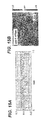
- FIG. 15A is a diagram showing the cross-sectional configuration of a surface of a substrate after it is polished by a polishing tool having a PV surface flatness of 0.1 to 1 ⁇ m
- FIG. 15B is a diagram showing an optical microscopic image of the surface of the substrate
- FIGS. 16A and 16B are diagrams illustrating different pulse voltages to be applied to a substrate
- FIG. 17 is a diagram showing an optical microscopic image of a surface of a GaN substrate after processing in Example 1;
- FIG. 18 is a diagram showing an optical microscopic image of the surface of the GaN substrate after processing in Example 1;
- FIG. 19 is a diagram showing an optical microscopic image of a surface of a GaN substrate after processing in Comp. Example 1;
- FIG. 20 is a diagram showing an optical microscopic image of a surface of a GaN substrate after processing in Comp. Example 2;
- FIG. 21 is a diagram showing an optical microscopic image of a surface of a GaN substrate after processing in Comp. Example 3;
- FIG. 22 is a diagram showing an optical microscopic image of a surface of a GaN substrate after processing in Comp. Example 4.
- FIG. 23 is a diagram showing an optical microscopic image of a surface of a GaN substrate after processing in Comp. Example 5;
- FIG. 24 is a diagram showing an optical microscopic image of a surface of a GaN substrate after processing in Comp. Example 6.
- FIG. 25 is a graph showing the relationship between Ga ion (Ga 3+ ion) concentration and polishing rate (removal rate).
- FIGS. 1A through 1D illustrate, in a sequence of process steps, a method for polishing and flattening, e.g., a surface of a GaN substrate while irradiating the surface with light according to the present invention.
- a processing solution 14 comprising a neutral pH buffer solution containing Ga ions
- the polishing tool 10 is, for example, composed of quartz glass which is an acidic solid catalyst having excellent light permeability.
- the processing solution 14 for example, a solution which is prepared by adding gallium nitrate to a phosphate buffer solution having a pH of 6.86 to bring Ga ions in the processing solution 14 near to saturation, in particular to a Ga ion concentration of not less than 10 ppm, followed by addition of a KOH solution to adjust the pH of the processing solution 14 in the range of 6.0 to 8.0.
- gallium nitrate it is possible to add another gallium salt, such as gallium hydrochloride, gallium phosphate, gallium sulfate, or gallium hydroxide.
- a substrate holder 18 holding a GaN substrate 16 with a front surface (surface to be processed) facing downwardly, is lowered to immerse the GaN substrate 16 in the processing solution 14 in the container 12 .
- light preferably ultraviolet light is emitted from a light source 20 disposed below the container 12 .
- Light passes though an opening 12 a , formed in a bottom plate of the container 12 , and through the interior of the polishing tool 10 , and reaches the front surface (lower surface) of the GaN substrate 16 .
- the wavelength of the irradiating light is preferably not more than the wavelength corresponding to the band gap of the object to be processed, GaN, i.e., not more than 365 nm (the band gap of GaN is 3.42 eV).
- GaN is oxidized by the light irradiation to produce Ga oxide (Ga 2 O 3 ) 16 a on the surface (lower surface) of the GaN substrate 16 , as shown in FIG. 1B .
- the GaN substrate 16 held by the substrate holder 18 is rotated and lowered to bring the surface of the Ga oxide 16 a into contact with the surface of the polishing tool 10 at a relatively low pressure, e.g., about 0.01 to 1.0 kgf/cm 2 , as shown in FIG. 1C .
- a relatively low pressure e.g., about 0.01 to 1.0 kgf/cm 2 , as shown in FIG. 1C .
- the Ga oxide 16 a formed in those portions of the substrate surface which are in contact with the polishing tool 10 i.e., formed at the tops of raised portions in the surface of the GaN substrate 16 having surface irregularities, is selectively processed and removed.
- the processing solution 14 comprises a neutral pH buffer solution containing Ga ions. Only a slight amount of Ga oxide 16 a can dissolve in such solution. Therefore, the Ga oxide 16 a , formed in recessed portions of the surface of the GaN substrate 16 having surface irregularities, can be prevented from dissolving in the processing solution 14 .
- only the Ga oxide 16 a formed at the tops of raised portions of the surface of the GaN substrate 16 , can be selectively removed while inhibiting dissolution of the Ga oxide 16 a , formed in recessed portions of the surface of the GaN substrate 16 , in the processing solution 14 . This can shorten the time it takes to flatten the surface of the GaN substrate 16 .
- quartz glass which is an acidic solid catalyst
- a large amount of hydrogen ions (H + ) are generated at the surface of the polishing tool (quartz glass) 10 .
- the Ga oxide 16 a formed in those portions of the substrate surface which are in contact with the polishing tool (quartz glass) 10 i.e., formed at the tops of raised portions in the surface of the GaN substrate 16 having surface irregularities, reacts with the hydrogen ions (H + ) in accordance with the above-described chemical equation (2) and dissolves in the processing solution 14 at a high rate.
- This can promote the reaction of removal of the Ga oxide 16 a at the tops of the raised portions in the surface of the GaN substrate 16 , thereby further shortening the time it takes to process and flatten the substrate surface.
- the polishing tool 10 In order to prevent adhesion of the GaN substrate 16 to the surface of the polishing tool 10 and efficiently supply the processing solution 14 to the surface of the GaN substrate 16 , it is preferred that the polishing tool 10 have a plurality of concentric, radial, spiral or lattice-shaped grooves in the surface.
- polishing tool 10 it is preferred to roughen a surface area of the polishing tool 10 which comes into contact with or close proximity to the GaN substrate 16 , e.g., by sandblasting, or to produce a fine pattern in the surface area, e.g., by dicing.
- This can prevent the formation of a layer (lubricating fluid film) of the processing solution 14 , which would hinder polishing, in a gap between the polishing tool 10 and the surface of the GaN substrate 16 .
- quartz glass which is an acidic solid catalyst
- a basic solid catalyst it is also possible to use a polishing tool 10 which has an acidic or basic solid catalyst layer at least in a surface area which comes into contact with or close to a substrate.
- the solid catalyst may be any of a non-woven fabric having an ion exchange function, a resin having an ion exchange function, a metal having an ion exchange function, and an acidic or basic metal oxide.
- the acidic or basic metal oxide include iron oxide, nickel oxide, cobalt oxide, tungsten oxide, ceramics such as alumina, zirconia and silica (silicon oxide), and glasses such as sapphire, quartz and zirconia.
- the processing solution 14 preferably contains metal oxide particles, diamond particles, or catalyst particles whose surfaces are modified with an acidic or basic functional group, or a mixture of these particles.
- the use of such particles can more efficiently remove the Ga oxide 16 a , thereby further shortening the time it takes to process and flatten a substrate surface.
- the metal oxide include silica (SiO 2 ) ceria (CeO 2 ), alumina (Al 2 O 3 ), zirconia (ZrO 2 ), tungsten oxide (WO 2 ), chromium oxide (Cr 2 O 3 ) and manganese dioxide (MnO 2 ).
- the catalyst particles whose surfaces are modified with an acidic or basic functional group may be exemplified by styrene resin or fluororesin particles whose surfaces are modified with a functional group, such as a sulfa group, a carboxyl group or an amino group.
- the processing solution 14 preferably contains an oxidizing agent.
- an oxidizing agent can promote the Ga oxide 16 a -producing reaction, thereby further shortening the time it takes to process and flatten a surface of a substrate.
- oxidizing agent examples include hydrogen peroxide water, ozone water, persulfates such as potassium persulfate and ammonium persulfate, permanganates such as potassium permanganate, perchromates such as potassium prechromate, vanadates such as ammonium vanadate, sodium vanadate and potassium vanadate, and iodates such as sodium orthoperiodate and sodium metaperiodate.
- the polishing method of this embodiment only those portions of the Ga oxide 16 a , which are in contact with the polishing tool 10 , are selectively processed. Thus, it becomes possible to process and flatten the surface of the GaN substrate 16 using the surface of the polishing tool 10 as a processing reference plane.
- the surface GaN of the GaN substrate 16 is oxidized by irradiating the substrate surface with light, preferably ultraviolet light, emitted from the light source 20 , it is also possible to oxidize the surface GaN of the GaN substrate 16 by applying a voltage between the polishing tool 10 and the GaN substrate 16 . It is preferred to use both the light irradiation and the voltage application.
- FIG. 2 shows the procedure of the experiment.
- a GaN substrate was cleaned with an aqueous solution of 3.5% HCl for 5 minutes.
- the mass (mass 1 ) of the GaN substrate was then measured.
- the GaN substrate was placed in a phosphate buffer solution, and a surface of the GaN substrate was irradiated with light for 60 minutes to produce a Ga oxide on the surface.
- the mass (mass 2 ) of the GaN substrate was then measured. Further, “etching component during light irradiation” was determined from the mass difference (mass 2 ⁇ mass 1 ).
- the GaN substrate was cleaned with an aqueous solution of 3.5% HCl for 5 minutes, followed by measurement of the mass (mass 3 ) of the GaN substrate. “Oxide component after light irradiation” was determined from the mass difference (mass 3 ⁇ mass 2 ).
- the “etching component during light irradiation” indicates the mass of Ga oxide that dissolved in the phosphate buffer solution during the light irradiation
- the “oxide component after light irradiation” indicates the mass of Ga oxide that dissolved in the aqueous solution of 3.5% HCl during the cleaning of the substrate with the HCl solution after the light irradiation.
- the GaN substrate was placed in the neutral (pH 7) phosphate buffer solution containing 10 ppm of Ga ions (“PBS/Ga (pH-7)”) and the surface of the substrate was irradiated with light
- PBS/Ga (pH-7) phosphate buffer solution containing 10 ppm of Ga ions
- the Ga oxide produced by the light irradiation did not dissolve in the phosphate buffer solution, and dissolved in the aqueous solution of 3.5% HCl when the substrate was cleaned with the HCl solution after the light irradiation.
- the Ga oxide produced by the light irradiation partly or wholly dissolved in the phosphate buffer solution.
- the experimental results thus indicate that the use, as a processing solution, of a neutral (pH 7) buffer solution containing Ga ions (e.g., 10 ppm) can inhibit dissolution of Ga oxide, produced on a surface of a GaN substrate, in the processing solution.
- a neutral (pH 7) buffer solution containing Ga ions e.g. 10 ppm
- FIG. 4 shows an optical microscopic image of the GaN substrate surface before the light irradiation
- FIG. 5 shows an optical microscopic image of the GaN substrate surface after the light irradiation.
- FIG. 6 shows an optical microscopic image of the GaN substrate surface after the light irradiation.
- FIG. 6 when a GaN substrate was placed in a phosphate buffer solution containing no Ga ions and a surface of the GaN substrate was irradiated with light, Ga oxide on the substrate surface dissolved in the solution, and hexagonal surface structures of a crystalline form called facet was formed.
- FIG. 7 is a plan view showing the overall construction of a flattening system incorporating a polishing apparatus according to an embodiment of the present invention.
- this flattening system includes a substantially rectangular housing 1 whose interior is divided by partition walls 1 a , 1 b , 1 c into a loading/unloading section 2 , a surface removal processing section 3 and a cleaning section 4 .
- the loading/unloading section 2 , the surface removal processing section 3 and the cleaning section 4 are independently fabricated and independently evacuated.
- the loading/unloading section 2 includes at least two (e.g., three as shown) front loading sections 200 on which substrate cassettes, each storing a number of substrates (objects to be polished), are placed.
- the front loading sections 200 are arranged side by side in the width direction (perpendicular to the long direction) of the flattening system.
- Each front loading section 200 can receive thereon an open cassette, a SMIF (standard manufacturing interface) pod or a FOUP (front opening unified pod).
- the SMIF and FOUP are a hermetically sealed container which can house a substrate cassette therein and can keep the interior environment independent of the exterior environment by covering with a partition.
- a moving mechanism 21 extending along the line of the front loading sections 200 , is provided in the loading/unloading section 2 .
- a first transfer robot 22 as a first transfer mechanism, which is movable along the direction in which substrate cassettes are arranged.
- the first transfer robot 22 can reach the substrate cassettes placed in the front loading sections 200 by moving on the moving mechanism 21 .
- the first transfer robot 22 has two hands, an upper hand and a lower hand, and can use the two hands differently, for example, by using the upper hand when returning a processed substrate to a substrate cassette and using the lower hand when transferring an unprocessed substrate.
- the loading/unloading section 2 is an area that needs to be kept in the cleanest environment. Accordingly, the interior of the loading/unloading section 2 is constantly kept at a higher pressure than any of the outside of the apparatus, the surface removal processing section 3 and the cleaning section 4 . Furthermore, a filter-fan unit (not shown) having an air filter, such as an HEPA filter or a ULPA filter, is provided above the moving mechanism 21 for the first transfer robot 22 . Clean air, from which particles, vapor and gas have been removed, continually blows off downwardly through the filter-fan unit.
- an air filter such as an HEPA filter or a ULPA filter
- the surface removal processing section 3 is an area where removal processing of a surface (surface to be processed) of a substrate is carried out.
- the surface removal processing section 3 includes a lapping apparatus 30 A as a first surface removal processing apparatus, a CMP apparatus 30 B as a second surface removal processing apparatus and two polishing apparatuses 30 C, 30 D according to an embodiment of the present invention as third (final) surface removal processing apparatuses.
- the lapping apparatus 30 A, the CMP apparatus 30 B and the polishing apparatuses 30 C, 30 D are arranged along the long direction of the flattening system.
- the lapping apparatus 30 A includes a platen 300 A having a lapping surface, a top ring 301 A for detachably holding a substrate and pressing the substrate against the platen 300 A, a lapping liquid supply nozzle 302 A for supplying a lapping liquid, such as a diamond slurry or a colloidal silica slurry, to the platen 300 A, and a pure water supply nozzle 303 A for supplying pure water to a surface of the platen 300 A.
- a lapping liquid supply nozzle 302 A for supplying a lapping liquid, such as a diamond slurry or a colloidal silica slurry
- the lapping liquid (slurry) is supplied from the lapping liquid supply nozzle 302 A onto the platen 300 A, and a substrate as a object to be polished is held by the top ring 301 A and pressed against the platen 300 A to carry out lapping of the surface of the substrate.
- the lapping apparatus 30 A is mainly directed to obtaining a large processing amount while enhancing the flatness of a substrate surface in the process of flattening, e.g., a substrate surface having relatively large initial irregularities into a desired flatness.
- the lapping apparatus 30 A can therefore be omitted when a substrate to be processed does not have large initial irregularities in a surface.
- the CMP apparatus 30 B includes a polishing table 300 B having a polishing surface, a top ring 301 B for detachably holding a substrate and pressing the substrate against the polishing table 300 B to polish the substrate, a polishing liquid supply nozzle 302 B for supplying a polishing liquid or a dressing liquid (e.g., water) to the polishing table 300 B, a dresser 303 B for carrying out dressing of the polishing surface of the polishing table 300 B, and an atomizer 304 B for spraying a mixed fluid of a liquid (e.g., pure water) and a gas (e.g., nitrogen gas) in a mist form onto the polishing surface of the polishing table 300 B from one or a plurality of nozzles.
- a liquid e.g., pure water
- a gas e.g., nitrogen gas
- a polishing liquid is supplied from the polishing liquid supply nozzle 302 B onto the polishing surface of the polishing table 300 B, and a substrate as an object to be polished is held by the top ring 301 B and pressed against the polishing surface to carry out polishing of the surface of the substrate.
- the CMP apparatus 30 B is to enhance the flatness of a substrate surface while processing the substrate at a high processing rate to obtain a large processing amount.
- the CMP apparatus 30 B when used in combination with the above-described lapping apparatus 30 A, can effectively flatten a substrate surface having relatively large initial irregularities into a desired flatness.
- the CMP apparatus 30 B may be omitted.
- the polishing apparatuses 30 C, 30 D each include a container 132 for holding therein a processing solution 130 comprising a neutral pH buffer solution containing Ga ions.
- a processing solution supply nozzle (processing solution supply section) 133 for supplying the processing solution 130 into the container 132 .
- the processing solution 130 may be used a solution which is prepared by adding Ga ions, e.g., in an amount of not less than 10 ppm, to a phosphate buffer solution, e.g., having a pH of 6.86 to bring Ga ions in the processing solution 130 near to saturation.
- the pH of the neutral pH buffer solution (at 25° C.) is, for example, 6.0 to 8.0.
- a polishing tool 134 is mounted on the bottom of the container 132 , so that the polishing tool 134 becomes immersed in the processing solution 130 when the processing solution 130 is filled into the container 132 .
- the polishing tool 134 is, for example, composed of quartz glass which is an acid solid catalyst having excellent light permeability. As described above, it is also possible to use a basic solid catalyst for the polishing tool 134 . Further, it is possible to use one having an acidic or basic solid catalyst layer only in a surface of the polishing tool 134 .
- the container 132 is coupled to an upper end of a rotating shaft 136 .
- the bottom plate of the container 132 has a ring-shaped opening 132 a formed around the rotating shaft 136 and closed by the polishing tool 134 .
- a reflective plate 138 having the 45° slant, is disposed right below the opening 134 a .
- a light source 140 for emitting light preferably ultraviolet light
- Light, preferably ultraviolet light, emitted from the light source 140 reflects off the reflective plate 138 , passes through the opening 132 a of the container 132 , permeates through the interior of the polishing tool 134 and reaches above the polishing tool 134 .
- a substrate holder 144 for detachably holding a substrate 142 , e.g., a GaN substrate, with a front surface facing downwardly.
- the substrate holder 144 is coupled to a lower end of a main shaft 146 that is rotatable and vertically movable.
- the rotating shaft 136 for rotating the container 132 and the main shaft 146 for rotating the substrate holder 144 constitute a movement mechanism for moving the polishing tool 134 and the substrate (GaN substrate) 142 , held by the substrate holder 144 , relative to each other.
- the polishing apparatus of this embodiment is also provided with a power source 148 for applying a voltage between the substrate 142 , held by the substrate holder 144 , and the polishing tool 134 .
- a switch 150 is interposed in a conducting wire 152 a extending from the positive pole of the power source 148 .
- processing of the substrate 142 is carried out in an immersion manner: the container 132 is filled with the processing solution 130 and the polishing tool 134 and the substrate 142 held by the substrate holder 144 are kept immersed in the processing solution 130 during processing. It is also possible to employ a dripping manner in which the processing solution 130 is supplied between the substrate 142 and the polishing tool 134 by dripping the processing solution 130 from the processing solution supply nozzle 133 onto the surface of the polishing tool 134 , so that processing of the substrate 142 is carried out in the presence of the processing solution 130 .
- the substrate holder 144 has a cover 160 for preventing intrusion of the processing solution 130 .
- a metal holder body 170 is coupled, via a rotation transmission section 168 including a universal joint 164 and a spring 166 , to a drive flange 162 that is coupled to the lower end of the main shaft 146 .
- a retainer ring 172 is vertically movably disposed around the lower portion of the holder body 170 .
- a conductive rubber 174 is mounted to a lower surface (substrate holding surface) of the holder body 170 such that a pressure space 176 can be formed between the lower surface of the holder body 170 and the conductive rubber 174 .
- An air introduction pipe 178 is connected to the pressure space 176 via an air introduction passage extending in the holder body 170 .
- the flange portion of the metal holder body 170 is provided with an extraction electrode 180 to which is connected the conducting wire 152 a extending from the positive pole of the power source 148 .
- At least the surface portion of the retainer ring 172 is preferably made of a glass material, such as quartz, sapphire or zirconia, or a ceramic material such as alumina, zirconia or silicon carbide.
- the conductive rubber 174 is, for example, a conductive chloroprene rubber, a conductive silicone rubber or a conductive fluororubber.
- the conductive rubber 174 comes into contact with the back surface of the substrate 142 to feed electricity to the back surface. While maintaining the electricity feeding to the back surface of the substrate 142 , air can be introduced into the pressure space 176 so as to press the substrate 142 against the polishing tool 134 .
- the substrate holder 144 can thus hold the substrate 142 while feeding electricity to the substrate 142 in a simple manner at a low resistance.
- the substrate holder 144 is preferably configured to be capable of filling a polar conductive grease between the conductive rubber 174 and the substrate 142 when bringing the substrate 142 into contact with the conductive rubber 174 upon holding of the substrate 142 on the substrate holder 144 .
- a large number of grooves 134 a are provided in an upper surface of the polishing tool 134 in an area corresponding to the opening 132 a of the container 132 .
- a vapor-deposited metal film 154 is formed in bottoms of the grooves 134 a .
- To the metal film 154 is connected a conducting wire 152 b extending from the negative pole of the power source 148 .
- the metal film 154 is preferably made of platinum or gold, which is corrosion-resistant.
- the grooves 134 a provided in the upper surface of the polishing tool 134 are preferably arranged in concentric circles, it is also possible to arrange the grooves in a spiral, radial or lattice-shaped configuration.
- a metal wire 156 of, e.g., gold or platinum in the bottoms of the grooves 134 provided in the upper surface of the polishing tool 134 .
- the grooves 134 a provided in the upper surface of the polishing tool 134 , e.g., into zones A to E in the radial direction of the substrate 142 to be held by the substrate holder 144 and brought into contact with the polishing tool 134 , and to individually control the voltages applied to the zones A to E. This makes it possible to control the polishing rate individually for the respective zones A to E.
- a heater 158 (see FIG. 8 ), embedded in the substrate holder 144 and extending into the rotating shaft 146 , is provided as a temperature control mechanism for controlling the temperature of the substrate 142 held by the substrate holder 144 .
- the processing solution supply nozzle 133 for supplying the processing solution 130 , which is controlled at a predetermined temperature by a heat exchanger as a temperature control mechanism, into the container 132 .
- a fluid passage (not shown) as a temperature control mechanism for controlling the temperature of the polishing tool 134 is provided in the interior of the polishing tool 134 .
- the processing rate can be adjusted and the stability of the processing rate can be enhanced.
- the polishing apparatuses 30 C, 30 D are each provided with a conditioning mechanism (conditioner) 190 , e.g., comprised of a polishing pad, for conditioning the surface (upper surface) of the polishing tool 134 so that it has desired flatness and appropriate roughness.
- the surface (upper surface) of the polishing tool 134 is conditioned by the conditioning mechanism (conditioner) 190 so that it has a PV (peak-to-valley) flatness of about 0.1 to 1 ⁇ m.
- an abrasive-containing slurry may be supplied to the surface of the polishing tool 134 , as necessary.
- the surface of the substrate when a surface of a substrate is polished by using a polishing tool having a PV surface flatness in the range of 0.1 to 1 ⁇ m, as shown in FIG. 15A , the surface of the substrate can be flatted (surface roughness RMS of the polished surface of the substrate is 0.337 ⁇ m). In addition, as shown in FIG. 15B , the polished surface of the substrate will be free of streaks.
- the substrate 142 such as a GaN substrate
- the substrate holder 144 lies above the container 132 , and the substrate holder 144 is then lowered to immerse the substrate 142 in the processing solution 130 held in the container 132 .
- light preferably ultraviolet light is radiated from the light source 140 onto the front surface (lower surface) of the substrate 142 .
- the wavelength of the irradiating light is preferably not more than the wavelength corresponding to the band gap of the substrate 142 , i.e., not more than 365 nm in the case of a GaN substrate (the band gap of GaN is 3.42 eV).
- GaN is thus oxidized by the light irradiation to produce Ga oxide (Ga 2 O 3 ) on the surface of the GaN substrate.
- the switch 150 of the power source 148 is turned on to apply a voltage between the polishing tool 134 and the substrate 142 , held by the substrate holder 144 , such that the polishing tool 134 serves as a cathode.
- the voltage application can promote the production of Ga oxide (Ga 2 O 3 ) on the surface of the GaN substrate.
- the rotating shaft 136 is rotated to rotate the polishing tool 134 and, at the same time, the substrate holder 144 is rotated to rotate the substrate 142 and lowered to bring the surface of the substrate 142 into contact with the surface of the polishing tool 134 preferably at a pressure of about 0.01 to 1.0 kgf/cm 2 . If the pressure is lower than 0.01 kgf/cm 2 , it is possible that warpage of the substrate 142 cannot be corrected and the entire substrate 142 cannot be polished uniformly.
- the radiation of light, preferably ultraviolet light, from the light source 140 and the voltage application between the polishing tool 134 and the substrate 142 are stopped, and the substrate holder 144 is raised and then the rotation of the substrate 142 is stopped.
- the processed substrate 142 is then transported for the next stage.
- Ga oxide on the surface of the substrate 142 is thus polished while forming a Ga oxide film on the surface of the substrate 142 both by irradiation of the surface of the substrate 142 with light and by application of a bias voltage to the substrate 142 . This can ensure a sufficient polishing rate and, even when there is a large damaged portion in the surface of the substrate 142 , can securely remove the damaged portion.
- the oxide film can grow faster than it is removed, resulting in excessive growth of the oxide film and attendant roughening of the surface of the substrate 142 .
- a first polishing step in the above-described manner, i.e., by polishing Ga oxide on the surface of the substrate 142 while forming the Ga oxide film on the substrate surface both by irradiation of the substrate surface with light and by application of a bias voltage to the substrate 142 , and to subsequently carry out a second polishing step without the application of the bias voltage while irradiating the surface of the substrate 142 with light.
- the first polishing step can ensure a sufficient polishing rate and, even when there is a large damaged portion in the surface of the substrate 142 , can securely remove the damaged portion.
- the second polishing step can prevent excessive growth of a Ga oxide film on the surface of the substrate 142 and can enhance the flatness of the processed surface of the substrate 142 .
- the bias voltage applied to the substrate 142 may be gradually decreased.
- a pulse voltage which repeats “on” and “off” at intervals of, e.g., 0.1 to 10 seconds, may be used as the bias voltage and the application off time of the pulse voltage may be gradually increased, as shown in FIG. 16A .
- processing of the surface of the substrate 142 can be carried out while applying a sufficiently high bias voltage to the substrate 142 so as to uniformly oxidize the entire surface of the substrate 142 and form a thin oxide film on the entire substrate surface without being influenced by a damaged portion in the substrate surface.
- a sufficiently high bias voltage to the substrate 142 so as to uniformly oxidize the entire surface of the substrate 142 and form a thin oxide film on the entire substrate surface without being influenced by a damaged portion in the substrate surface.
- first polishing step and the second polishing step are carried out successively in the same apparatus to increase the throughput, it is also possible to use separate apparatuses to carry out the first and second polishing steps.
- a first linear transporter 5 as a second (translatory) transfer mechanism for transferring a substrate between four transferring positions (a first transferring position TP 1 , a second transferring position TP 2 , a third transferring position TP 3 , and a fourth transferring position TP 4 in the order of distance from the loading/unloading section 2 ) along the long direction of the flattering system.
- a reversing machine 31 for reversing a substrate received from the first transfer robot 22 is disposed above the first transferring position TP 1 of the first linear transporter 5 , and a vertically-movable lifter 32 is disposed below the reversing machine 31 . Further, a vertically-movable pusher 33 is disposed below the second transferring position TP 2 , a vertically-movable pusher 34 is disposed below the third transferring position TP 3 , and a vertically-movable lifter 35 is disposed below the fourth transferring position TP 4 .
- a second linear transporter 6 Beside the polishing apparatuses 30 C, 30 D and adjacent to the first linear transporter 5 is disposed a second linear transporter 6 as a second (translatory) transfer mechanism for transferring a substrate between three transferring positions (fifth transferring position TP 5 , sixth transferring position TP 6 and seventh transferring position TP 7 in order of distance from the loading/unloading section 2 ) along the long direction of the flattering system.
- a vertically-movable lifter 36 is disposed below the fifth transferring position TP 5
- a pusher 37 is disposed below the sixth transferring position TP 6
- a pusher 38 is disposed below the seventh transferring position TP 7 .
- a pure water replacement section 192 including a tub and a pure water nozzle is disposed between the polishing apparatus 30 C and the pusher 37
- a pure water replacement section 194 including a tub and a pure water nozzle is also disposed between the polishing apparatus 30 D and the pusher 38 .
- the surface removal processing section 3 is the dirtiest area. In this system, therefore, discharge of air is performed around a removal processing site, such as a platen, so as to prevent particles in the surface removal processing section 3 from flying to the outside. Further, the internal pressure of the surface removal processing section 3 is made lower than the external pressure of the system and the internal pressures of the neighboring cleaning section 4 and loading/unloading section 2 , thereby preventing particles from flying out.
- An exhaust duct (not shown) and a filter (not shown) are usually provided respectively below and above a removal processing site, such as a platen, so as to create a downward flow of cleaned air.
- the cleaning section 4 is an area for cleaning a substrate.
- the cleaning section 4 includes a second transfer robot 40 , a reversing machine 41 for reversing a substrate received from the second transfer robot 40 , three cleaning units 42 - 44 each for cleaning the substrate, a drying unit 45 for rinsing the cleaned substrate with pure water and then spin-drying the substrate, and a movable third transfer robot 46 for transferring the substrate between the reversing machine 41 , the cleaning units 42 - 44 and the drying unit 45 .
- the second transfer robot 40 , the reversing machine 41 , the cleaning units 42 - 44 and the drying unit 45 are arranged in a line along the long direction of the flattering system, and the third transfer robot 46 is movably disposed between the first linear transporter 5 and the line of the second transfer robot 40 , the reversing machine 41 , the cleaning units 42 - 44 and the drying unit 45 .
- a filter-fan unit (not shown) having an air filter is provided above the cleaning units 42 - 44 and the drying unit 45 , and clean air, from which particles have been removed by the filter-fan unit, continually blows downward.
- the interior of the cleaning section 4 is constantly kept at a higher pressure than the surface removal processing section 3 to prevent inflow of particles from the surface removal processing section 3 .
- a shutter 50 located between the reversing machine 31 and the first transfer robot 22 , is provided in the partition wall 1 a surrounding the surface removal processing section 3 .
- the shutter 50 is opened when transferring a substrate between the first transfer robot 22 and the reversing machine 31 .
- a shutter 53 located at a position facing the CMP apparatus 30 B and a shutter 54 located at a position facing the polishing apparatus 30 C are respectively provided in the partition wall 1 b surrounding the surface removal processing section 3 .
- One substrate is taken by the first transfer robot 22 out of a substrate cassette mounted in one of the front loading sections 20 , and the substrate is transferred to the reversing machine 31 .
- the reversing machine 31 reverses the substrate 180° and then places the substrate on the lifter 32 at the first transferring position TP 1 .
- the top ring 301 A of the lapping apparatus 30 A receives the substrate from the lifter 32 , and the lapping apparatus 30 A carries out lapping of the surface of the substrate.
- lapping of the substrate surface is carried out, e.g., at a processing rate of not more than several tens of ⁇ m/h while supplying a lapping liquid, such as a diamond slurry or a colloidal silica slurry, to the platen 300 A, thereby removing the substrate surface in an amount corresponding to a thickness of about 10 ⁇ m and flattening the substrate surface.
- a lapping liquid such as a diamond slurry or a colloidal silica slurry
- the substrate after lapping is transferred to the pusher 33 at the second transferring position TP 2 , and is then transferred to the third transferring position TP 3 by the first linear transporter 5 .
- the top ring 301 B of the CMP apparatus 30 B receives the substrate from the pusher 34 at the third transferring position TP 3 , and the CMP apparatus 30 B carries out chemical mechanical polishing of the surface of the substrate.
- chemical mechanical polishing of the substrate surface is carried out, e.g., at a processing rate of not more than several ⁇ m/h while supplying a polishing liquid, e.g., containing colloidal silica, to the polishing table 300 B, thereby removing the substrate surface in an amount corresponding to a thickness of about several ⁇ m and further flattening the substrate surface.
- the depth of damage in the substrate surface after processing is about 10 nm.
- the substrate surface is rinsed with pure water, as necessary.
- the substrate after CMP is transferred to the lifter 35 at the fourth transferring position TP 4 .
- the second transfer robot 40 receives the substrate from the lifter 35 and places the substrate on the lifter 36 at the fifth transferring position TP 5 .
- the second linear transporter 6 moves horizontally to transfer the substrate on the lifter 36 to one of the sixth transferring position TP 6 and the seventh transferring position TP 7 .
- the substrate holder 144 of the polishing apparatus 30 C or 30 D receives the substrate from the pusher 37 or 38 , and the polishing apparatus 30 C or 30 D carries out polishing of the surface of the substrate.
- a processing solution remaining on the substrate surface after polishing is replaced with pure water in the pure water replacement section 192 , and the substrate is then returned to the sixth transferring position TP 6 .
- a processing solution remaining on the substrate surface after polishing is replaced with pure water in the pure water replacement section 194 , and the substrate is then returned to the seventh transferring position TP 7 .
- the substrate after pure water replacement is moved to the fifth transferring position TP 5 by the second linear transporter 6 .
- the second transfer robot 40 takes the substrate out of the fifth transferring position TP 5 and transfers the substrate to the reversing machine 41 .
- the reversing machine 41 reverses the substrate 180° and then transfers it to the first cleaning unit 42 , where the substrate is cleaned.
- the third transfer robot 46 transfers the substrate from the first cleaning unit 42 to the second cleaning unit 43 , where the substrate is cleaned.
- the third transfer robot 46 transfers the substrate after cleaning to the third cleaning unit 44 , where the substrate is cleaned with pure water.
- the third transfer robot 46 transfers the substrate after pure water cleaning to the drying unit 45 , where the substrate is rinsed with pure water and then rotated at a high speed to spin-dry the substrate.
- the first transfer robot 22 receives the substrate after spin-drying from the drying unit 45 and returns the substrate to the substrate cassette mounted in the front loading section 200 .
- FIG. 8 Using the polishing apparatus shown in FIG. 8 and using, as a processing solution, a phosphate buffer solution having a pH of 6.86 and containing 10 ppm of Ga ions, polishing of a surface of a Ga substrate was carried out with a polishing tool, composed of quartz glass which is an acidic solid catalyst, for 3 hours while irradiating the surface with ultraviolet light, having a peak emission wavelength of 365 nm, emitted from a light source.
- FIGS. 17 and 18 show optical microscopic images of the surface of the GaN substrate after processing.
- Polishing of a surface of a GaN substrate was carried out in the same manner as in Example 1, except for using a processing solution which was the same as the processing solution used in Example 1, but whose pH was changed to 1 with hydrochloric acid (Comp. Example 1); and a processing solution which was the same as the processing solution used in Example 1, but whose pH was changed to 13 with potassium hydroxide (Comp. Example 2).
- FIGS. 19 and 20 show optical microscopic images of the surfaces of the GaN substrates after processing in Comp. Examples 1 and 2.
- Polishing of a surface of a GaN substrate was carried out in the same manner as in Example 1, except for using a processing solution which was the same as the processing solution used in Example 1, but whose pH was changed to 5 with phosphoric acid (HPO 3 ) (Comp. Example 3); and a processing solution which was the same as the processing solution used in Example 1, but whose pH was changed to 9 with potassium hydroxide (Comp. Example 4).
- FIGS. 21 and 22 show optical microscopic images of the surfaces of the GaN substrates after processing in Comp. Examples 3 and 4.
- the use of a neutral processing solution having a pH of 6 to 8, in particular 6.86 can provide a processed surface having lower roughness as compared to the use of an acidic or basic processing solution.
- FIG. 23 shows an optical microscopic image of the surface of the GaN substrate after processing.
- the surface roughness (RMS: 0.404 nm) of the processed substrate of Example 1 is significantly lower than the surface roughness (RMS: 11.662 nm) of the processed substrate of Comp. Example 5. This indicates that the inclusion of Ga ions in a neutral buffer solution can significantly improve the surface roughness of a processed surface.
- FIG. 24 shows an optical microscopic image of the surface of the GaN substrate after processing.
- the surface roughness (RMS: 0.636 nm) of the processed substrate of Comp. Example 6, in which the processing was carried out for 40 hours using the processing solution containing no Ga ions, is almost equal to that of Example 1 in which the processing was carried out for 3 hours using the processing solution containing Ga ions. This indicates that the inclusion of Ga ions in a neutral buffer solution can significantly shorten the time it takes to polish and flatten a surface of a GaN substrate.
- FIG. 25 shows the relationship between the Ga ion (Ga 3+ ion) concentration and the polishing rate (removal rate). As can be seen from FIG. 25 , the processing (polishing) rate decreases with increase in the Ga ion concentration.
- the processed surface has a high surface roughness RMS of not less than 5 nm, whereas the surface roughness RMS of the processed surface is as low as not more than 1 nm at a Ga ion concentration of not less than 10 ppm. This is considered to be due to the fact that the inclusion of an effective amount of Ga ions in the solution inhibits isotropic etching of the surface oxide in recessed portions of the substrate surface, whereby only raised portions of the substrate surface are removed catalytically.
- the Ga ion concentration of a processing solution is preferably not less than 10 ppm. If the Ga ion concentration is less than 10 ppm, the surface roughness of a processed substrate will be high or poor as shown in FIG. 23 . On the other hand, the Ga ion concentration of a processing solution is preferably not more than 100 ppm, because a processing solution can turn into a gel when the Ga ion concentration is more than 100 ppm.
- the present invention is applicable to a polishing method and a polishing apparatus for processing and flattening a surface (surface to be processed) of a substrate, such as an elemental substrate of a compound semiconductor containing Ga (gallium) element or a bonded substrate (epitaxial substrate) having a layer of Ga element-containing compound semiconductor.
Applications Claiming Priority (5)
| Application Number | Priority Date | Filing Date | Title |
|---|---|---|---|
| JP2009-078234 | 2009-03-27 | ||
| JP2009078234 | 2009-03-27 | ||
| JP2009284492A JP5364959B2 (ja) | 2009-03-27 | 2009-12-15 | 研磨方法及び研磨装置 |
| JP2009-284492 | 2009-12-15 | ||
| PCT/JP2010/055484 WO2010110463A1 (en) | 2009-03-27 | 2010-03-19 | POLISHING METHOD, POLISHING APPARATUS AND GaN WAFER |
Publications (2)
| Publication Number | Publication Date |
|---|---|
| US20120001193A1 US20120001193A1 (en) | 2012-01-05 |
| US9233449B2 true US9233449B2 (en) | 2016-01-12 |
Family
ID=42781154
Family Applications (1)
| Application Number | Title | Priority Date | Filing Date |
|---|---|---|---|
| US13/138,635 Active 2030-04-13 US9233449B2 (en) | 2009-03-27 | 2010-03-19 | Polishing method, polishing apparatus and GaN wafer |
Country Status (5)
| Country | Link |
|---|---|
| US (1) | US9233449B2 (ja) |
| EP (1) | EP2412009A4 (ja) |
| JP (1) | JP5364959B2 (ja) |
| KR (1) | KR20120009468A (ja) |
| WO (1) | WO2010110463A1 (ja) |
Cited By (3)
| Publication number | Priority date | Publication date | Assignee | Title |
|---|---|---|---|---|
| US20180265989A1 (en) * | 2017-03-17 | 2018-09-20 | Toshiba Memory Corporation | Substrate treatment apparatus and substrate treatment method |
| TWI671436B (zh) * | 2017-03-17 | 2019-09-11 | 日商東芝記憶體股份有限公司 | 基板處理裝置及基板處理方法 |
| US10879087B2 (en) * | 2017-03-17 | 2020-12-29 | Toshiba Memory Corporation | Substrate treatment apparatus and manufacturing method of semiconductor device |
Families Citing this family (14)
| Publication number | Priority date | Publication date | Assignee | Title |
|---|---|---|---|---|
| US7776228B2 (en) * | 2006-04-11 | 2010-08-17 | Ebara Corporation | Catalyst-aided chemical processing method |
| WO2011074691A1 (en) | 2009-12-15 | 2011-06-23 | Osaka University | Polishing method, polishing apparatus and polishing tool |
| TWI613037B (zh) | 2011-07-19 | 2018-02-01 | 荏原製作所股份有限公司 | 硏磨方法 |
| JPWO2013021946A1 (ja) * | 2011-08-09 | 2015-03-05 | 株式会社フジミインコーポレーテッド | 化合物半導体研磨用組成物 |
| CN106256016B (zh) * | 2014-04-18 | 2020-06-23 | 株式会社荏原制作所 | 基板处理装置、基板处理系统 |
| JP6346124B2 (ja) | 2015-06-02 | 2018-06-20 | 東芝メモリ株式会社 | 半導体装置の製造方法 |
| JP6797409B2 (ja) * | 2017-01-12 | 2020-12-09 | 国立大学法人大阪大学 | 触媒表面基準エッチング方法及びその装置 |
| JP6329655B2 (ja) * | 2017-02-06 | 2018-05-23 | 国立大学法人大阪大学 | 陽極酸化を援用した研磨方法 |
| CN108890509A (zh) * | 2018-07-25 | 2018-11-27 | 浙江工业大学 | 光催化钴基合金加工平台及加工方法 |
| WO2020194944A1 (ja) * | 2019-03-27 | 2020-10-01 | Agc株式会社 | 酸化ガリウム基板の製造方法、および酸化ガリウム基板用の研磨スラリー |
| KR102253176B1 (ko) * | 2019-11-13 | 2021-05-14 | 에임즈마이크론 주식회사 | GaN 기판 처리 방법, 이에 의해 처리된 GaN 기판 및 이를 수행하는 GaN 기판 처리 장치 |
| CN114664972B (zh) * | 2020-12-23 | 2024-04-16 | 比亚迪股份有限公司 | 一种硅片的抛光方法、太阳能电池片的制备方法及太阳能电池片 |
| JP2023106084A (ja) * | 2022-01-20 | 2023-08-01 | 株式会社デンソー | チャック装置 |
| CN115650478A (zh) * | 2022-10-09 | 2023-01-31 | 大连理工大学 | 复合型化学机械抛光和抛光液循环处理一体化的设备及处理方法 |
Citations (11)
| Publication number | Priority date | Publication date | Assignee | Title |
|---|---|---|---|---|
| JP2001205555A (ja) | 1999-11-16 | 2001-07-31 | Denso Corp | メカノケミカル研磨方法及びメカノケミカル研磨装置 |
| US20050269577A1 (en) * | 2004-06-08 | 2005-12-08 | Matsushita Electric Industrial Co., Ltd. | Surface treatment method and surface treatment device |
| JP2007283410A (ja) | 2006-04-12 | 2007-11-01 | Kumamoto Univ | 触媒支援型化学加工方法 |
| EP1894900A2 (en) | 2006-08-28 | 2008-03-05 | Osaka University | Catalyst-aided chemical processing method and apparatus |
| JP2008081389A (ja) | 2006-08-28 | 2008-04-10 | Osaka Univ | 触媒支援型化学加工方法及び装置 |
| JP2008121099A (ja) * | 2006-10-18 | 2008-05-29 | Osaka Univ | 触媒支援型化学加工方法及び装置 |
| JP2008166709A (ja) | 2006-12-05 | 2008-07-17 | Ebara Corp | 基板研磨装置、及び基板研磨設備 |
| US7501346B2 (en) * | 2006-07-21 | 2009-03-10 | Cabot Microelectronics Corporation | Gallium and chromium ions for oxide rate enhancement |
| JP2009067620A (ja) | 2007-09-12 | 2009-04-02 | Hitachi Cable Ltd | 化合物半導体単結晶の製造方法及びその製造装置 |
| US20090095712A1 (en) | 2007-10-15 | 2009-04-16 | Ebara Corporation | Flattening method and flattening apparatus |
| US7776228B2 (en) | 2006-04-11 | 2010-08-17 | Ebara Corporation | Catalyst-aided chemical processing method |
-
2009
- 2009-12-15 JP JP2009284492A patent/JP5364959B2/ja active Active
-
2010
- 2010-03-19 KR KR1020117025366A patent/KR20120009468A/ko active Search and Examination
- 2010-03-19 US US13/138,635 patent/US9233449B2/en active Active
- 2010-03-19 WO PCT/JP2010/055484 patent/WO2010110463A1/en active Application Filing
- 2010-03-19 EP EP10756259.7A patent/EP2412009A4/en not_active Withdrawn
Patent Citations (13)
| Publication number | Priority date | Publication date | Assignee | Title |
|---|---|---|---|---|
| JP2001205555A (ja) | 1999-11-16 | 2001-07-31 | Denso Corp | メカノケミカル研磨方法及びメカノケミカル研磨装置 |
| US20050269577A1 (en) * | 2004-06-08 | 2005-12-08 | Matsushita Electric Industrial Co., Ltd. | Surface treatment method and surface treatment device |
| US7776228B2 (en) | 2006-04-11 | 2010-08-17 | Ebara Corporation | Catalyst-aided chemical processing method |
| JP2007283410A (ja) | 2006-04-12 | 2007-11-01 | Kumamoto Univ | 触媒支援型化学加工方法 |
| US7501346B2 (en) * | 2006-07-21 | 2009-03-10 | Cabot Microelectronics Corporation | Gallium and chromium ions for oxide rate enhancement |
| US7651625B2 (en) | 2006-08-28 | 2010-01-26 | Osaka University | Catalyst-aided chemical processing method and apparatus |
| EP1894900A2 (en) | 2006-08-28 | 2008-03-05 | Osaka University | Catalyst-aided chemical processing method and apparatus |
| US20080073222A1 (en) | 2006-08-28 | 2008-03-27 | Kazuto Yamauchi | Catalyst-aided chemical processing method and apparatus |
| JP2008081389A (ja) | 2006-08-28 | 2008-04-10 | Osaka Univ | 触媒支援型化学加工方法及び装置 |
| JP2008121099A (ja) * | 2006-10-18 | 2008-05-29 | Osaka Univ | 触媒支援型化学加工方法及び装置 |
| JP2008166709A (ja) | 2006-12-05 | 2008-07-17 | Ebara Corp | 基板研磨装置、及び基板研磨設備 |
| JP2009067620A (ja) | 2007-09-12 | 2009-04-02 | Hitachi Cable Ltd | 化合物半導体単結晶の製造方法及びその製造装置 |
| US20090095712A1 (en) | 2007-10-15 | 2009-04-16 | Ebara Corporation | Flattening method and flattening apparatus |
Non-Patent Citations (26)
| Title |
|---|
| Akihisa Kubota, Keita Yagi, Junji Murata, Heiji Yasui, Shiro Miyamoto, Hideyuki Hara, Yasuhisa Sano and Kazuto Yamauchi, "Polishing Characteristics of Single Crystal SiC Surface Finished by Fe-Catalyst Rod under H2O2 Solution", Extended Abstracts of International 21st Century COE Symposium on Atomistic Fabrication Technology 2007, pp. 129-130 (Oct. 15-17, 2007, Osaka, Japan). |
| Bardwell et al., "Ultraviolet Photoenhanced Wet Etching of GaN in K2S2O8 Solution", Journal of Applied Physics, vol. 89, No. 7, Apr. 1, 2001, pp. 4142-4149. |
| H. Hara, Y. Morikawa, Y. Sano, and K. Yamauchi, "First-Principles Calculation of Surface Energy at 4H-SiC(0001)-1×1", Extended Abstracts of First International Symposium on Atomically Controlled Fabrication Technology-Surface and Thin Film Processing-, pp. 62-63 (Feb. 16-17, 2009, Osaka, Japan). |
| H. Hara, Y. Sano, K. Arima, K. Yagi, J. Murata, A. Kubota, H. Mimura and K. Yamauchi, "Development of CAtalyst-Referred Etching", Extended Abstracts of International 21st Century COE Symposium on Atomistic Fabrication Technology, pp. 27-28 (Oct. 19-20, 2006, Osaka, Japan). |
| Hideyuki Hara, Yasuhisa Sano, Hidekazu Mimura, Kenta Arima, Akihisa Kubota, Keita Yagi, Junji Murata and Kazuto Yamauchi, "Damage-Free Planarization of 4H-SiC (0001) by Catalyst-Referred Etching", Programme of the 6th European Conference on Silicon Carbide and Related Materials (ECSCRM 2006), p. 28 (Sep. 3-7, 2006, Newcastle upon Tyne, UK). |
| Hideyuki Hara, Yasuhisa Sano, Hidekazu Mimura, Kenta Arima, Akihisa Kubota, Keita Yagi, Junji Murata and Kazuto Yamauchi, "Novel Abrasive-Free Planarization of Si and SiC Using Catalyst", The 11th International Conference on Precision Engineering (ICPE), pp. 267-270 (Aug. 16-18, 2006, Tokyo, Japan). |
| Hideyuki Hara, Yasuhisa Sano, Kenta Arima, Keita Yagi, Junji Murata, Takeshi Okamoto, Hidekazu Mimura and Kazuto Yamauchi, "New Crystal Planarization Technique Using a Catalyst Plate", Proceedings of 15th International Conference on Crystal Growth, Abstract#769 (Aug. 12-17, 2007, Salt Lake City, USA). |
| Hideyuki Hara, Yasuhisa Sano, Takeshi Okamoto, Kenta Arima, Keita Yagi, Junji Murata, Akihisa Kubota, Hidekazu Mimura, Kazuto Yamauchi, "Planarization Mechanism of Catalyst-Referred Etching", Extended Abstracts of International 21st Century COE Symposium on Atomistic Fabrication Technology 2007, pp. 37-38 (Oct. 15-17, 2007, Osaka, Japan). |
| International Search Report issued Jun. 15, 2010 in International (PCT) Application No. PCT/JP2010/055484. |
| J. Murata, A. Kubota, K. Yagi, Y. Sano, H. Hara, K. Arima, T. Okamoto, H. Mimura and K. Yamauchi, "New Chemical Planarization of SiC and GaN Using Fe Plate in H2O2 Solution", International Conference on Silicon Carbide and Related Materials 2007, Technical Digest (ICSCRM 2007), pp. Th-13-Th-14 (Oct. 14-19, 2007, Otsu, Japan). |
| J. Murata, S. Sadakuni, K. Yagi, H. Hara, K. Arima, T. Okamoto, H. Mimura and K. Yamauchi, "Photo-Enhanced Chemical Planarization of Gallium Nitride Using a Solid Acidic Catalyst", Extended Abstracts of First International Symposium on Atomically Controlled Fabrication Technology-Surface and Thin Film Processing-, pp. 60-61 (Feb. 16-17, 2009, Osaka, Japan). |
| Junji Murata, Akihisa Kubota, Keita Yagi, Yasuhisa Sano, Hideyuki Hara, Kenta Arima, Takeshi Okamoto, Hidekazu Mimura and Kazuto Yamauchi, "Damage-Free Planarization of GaN Using a Catalyst Plate", Proceedings of 15th International Conference on Crystal Growth, Abstract#789 (Aug. 12-17, 2007, Salt Lake City, USA). |
| Junji Murata, Akihisa Kubota, Keita Yagi, Yasuhisa Sano, Hideyuki Hara, Kenta Arima, Takeshi Okamoto, Hidekazu Mimura and Kazuto Yamauchi, "Novel Abrasive-Free Planarization of GaN Using a Catalytic Reference Plate", Extended Abstracts of International 21st Century COE Symposium on Atomistic Fabrication Technology 2007, pp. 127-128 (Oct. 15-17, 2007, Osaka, Japan). |
| K. Yagi, J. Murata, H. Hara, Y. Sano, K. Yamauchi and H. Goto, "Fabrication of Damascene Cu Wiring Using Solid Acid Catalyst", Extended Abstracts of International 21st Century COE Symposium on Atomistic Fabrication Technology, pp. 85-86 (Oct. 19-20, 2006, Osaka, Japan). |
| K. Yamauchi, Y. Sano, K. Arima, H. Hara, J. Murata, K. Yagi and T. Okamoto, "Catalyst-Referred Etching-Damage-Free Planarization of 4H-SiC (0001)", 4th International Workshop on Crystal Growth Technology, p. 87 (May 18-25, 2008, Beatenberg above Interlaken, Switzerland). |
| Keita Yagi, Junji Murata, Yasuhisa Sano, Hideyuki Hara, Kenta Arima, Takeshi Okamoto, Hidekazu Mimura and Kazuto Yamauchi, "Damage-Free Planarization of 4H-SiC Using Catalyst Plate", Proceedings of 15th International Conference on Crystal Growth, Abstract#859 (Aug. 12-17, 2007, Salt Lake City, USA). |
| Keita Yagi, Yasuhisa Sano, Hideyuki Hara, Junji Murata, Kenta Arima, Takeshi Okamoto, Hidekazu Mimura and Kazuto Yamauchi, "Development of Planarization Equipment Using Catalyst-Referred Etching", Extended Abstracts of International 21st Century COE Symposium on Atomistic Fabrication Technology 2007, pp. 35-36 (Oct. 15-17, 2007, Osaka, Japan). |
| Kenta Arima and Mizuho Morita, "Atomic-Scale Characterization of Semiconductor Surfaces after Wet Cleaning", Extended Abstracts of International 21st Century COE Symposium on Atomistic Fabrication Technology, pp. 59-60 (Oct. 19-20, 2006, Osaka, Japan). |
| Kenta Arima and Mizuho Morita, "Development of Wet-Chemical Procedures to Control Emerging Semiconductor Surfaces on the Atomic Scale", Extended Abstracts of International 21st Century COE Symposium on Atomistic Fabrication Technology 2007, pp. 51-52 (Oct. 15-17, 2007, Osaka, Japan). |
| Kenta Arima, Ryosuke Suga, Hideyuki Hara, Junji Murata, Keita Yagi, Hidekazu Mimura, Yasuhisa Sano and Kazuto Yamauchi, "Atomically Resolved STM Study of 4H-SiC (0001) Surfaces Flattened by Chemical Etching in HF Solutions with Pt Catalyst", International Conference on Silicon Carbide and Related Materials 2007, Technical Digest (ICSCRM 2007), pp. We-28-We-29 (Oct. 14-19, 2007, Otsu, Japan). |
| Ryota Okamoto, Kenta Arima, Hideyuki Hara, Yasuhisa Sano, Takeshi Ishida, Keita Yagi, Akihisa Kubota, Katsuyoshi Endo and Kazuto Yamauchi, "Scanning Tunneling Microscopy Study of 4H-SiC (0001) Surfaces After Wet-Chemical Preparations", Extended Abstracts of International 21st Century COE Symposium on Atomistic Fabrication Technology, pp. 125-126 (Oct. 19-20, 2006, Osaka, Japan). |
| Supplementary European Search Report dated Jun. 17, 2013 in corresponding European Patent Application No. 10756259.7. |
| T. Okamoto, Y. Sano, H. Hara, K. Arima, K. Yagi, J. Murata, H. Mimura and K. Yamauchi, "Damage-Free Planarization of 2-inch 4H-SiC Wafer Using Pt Catalyst Plate and HF Solution", International Conference on Silicon Carbide and Related Materials 2007, Technical Digest (ICSCRM 2007), pp. We-94-We-95 (Oct. 14-19, 2007, Otsu, Japan). |
| T. Okamoto, Y. Sano, H. Hara, T. Hatayama, K. Arima, K. Yagi, J. Murata, H. Mimura, T. Fuyuki and K. Yamauchi, "Novel Abrasive-Free Chemical Planarization of 4H-SiC 8°off Wafer Using a Catalyst", Extended Abstracts of First International Symposium on Atomically Controlled Fabrication Technology-Surface and Thin Film Processing-, pp. 64-65 (Feb. 16-17, 2009, Osaka, Japan). |
| Written Opinion of the International Searching Authority issued Jun. 15, 2010 in International (PCT) Application No. PCT/JP2010/055484. |
| Y. Sano, K. Yamamura and K. Yamauchi, "Development of Ultraprecision Machining Technologies for Semiconductor Substrates", Extended Abstracts of First International Symposium on Atomically Controlled Fabrication Technology-Surface and Thin Film Processing-, pp. 16-17 (Feb. 16-17, 2009, Osaka, Japan). |
Cited By (4)
| Publication number | Priority date | Publication date | Assignee | Title |
|---|---|---|---|---|
| US20180265989A1 (en) * | 2017-03-17 | 2018-09-20 | Toshiba Memory Corporation | Substrate treatment apparatus and substrate treatment method |
| TWI671436B (zh) * | 2017-03-17 | 2019-09-11 | 日商東芝記憶體股份有限公司 | 基板處理裝置及基板處理方法 |
| US10879087B2 (en) * | 2017-03-17 | 2020-12-29 | Toshiba Memory Corporation | Substrate treatment apparatus and manufacturing method of semiconductor device |
| US11784064B2 (en) | 2017-03-17 | 2023-10-10 | Kioxia Corporation | Substrate treatment apparatus and manufacturing method of semiconductor device |
Also Published As
| Publication number | Publication date |
|---|---|
| JP5364959B2 (ja) | 2013-12-11 |
| WO2010110463A1 (en) | 2010-09-30 |
| JP2010251699A (ja) | 2010-11-04 |
| KR20120009468A (ko) | 2012-02-21 |
| US20120001193A1 (en) | 2012-01-05 |
| EP2412009A4 (en) | 2013-07-17 |
| EP2412009A1 (en) | 2012-02-01 |
Similar Documents
| Publication | Publication Date | Title |
|---|---|---|
| US9233449B2 (en) | Polishing method, polishing apparatus and GaN wafer | |
| US10916455B2 (en) | Flattening method and flattening apparatus | |
| US8912095B2 (en) | Polishing method, polishing apparatus and polishing tool | |
| JP5248671B2 (ja) | 平坦化方法 | |
| JP5403359B2 (ja) | 研磨具及び研磨装置 | |
| JP5552648B2 (ja) | 研磨方法及び研磨装置 | |
| US11220757B2 (en) | Method for manufacturing solid oxide and device therefor | |
| US20060118935A1 (en) | Laminated semiconductor substrate process for producing the same | |
| JP6206847B2 (ja) | ワイドバンドギャップ半導体基板の加工方法及びその装置 | |
| JP2015128161A (ja) | 研磨方法 | |
| JP2013017925A (ja) | 光触媒反応型化学的加工方法及び装置 | |
| JP7181818B2 (ja) | 光触媒を用いた基板処理装置および基板処理方法 | |
| JP2011125938A (ja) | 研磨方法及び研磨装置 | |
| JP2000049125A (ja) | 半導体シリコン単結晶ウェーハの研磨方法 | |
| KR20050028229A (ko) | 웨이퍼의 제조방법 및 웨이퍼의 연마장치 |
Legal Events
| Date | Code | Title | Description |
|---|---|---|---|
| AS | Assignment |
Owner name: EBARA CORPORATION, JAPAN Free format text: ASSIGNMENT OF ASSIGNORS INTEREST;ASSIGNORS:SANO, YASUHISA;YAMAUCHI, KAZUTO;MURATA, JUNJI;AND OTHERS;REEL/FRAME:027012/0054 Effective date: 20110803 Owner name: OSAKA UNIVERSITY, JAPAN Free format text: ASSIGNMENT OF ASSIGNORS INTEREST;ASSIGNORS:SANO, YASUHISA;YAMAUCHI, KAZUTO;MURATA, JUNJI;AND OTHERS;REEL/FRAME:027012/0054 Effective date: 20110803 |
|
| STCF | Information on status: patent grant |
Free format text: PATENTED CASE |
|
| MAFP | Maintenance fee payment |
Free format text: PAYMENT OF MAINTENANCE FEE, 4TH YEAR, LARGE ENTITY (ORIGINAL EVENT CODE: M1551); ENTITY STATUS OF PATENT OWNER: LARGE ENTITY Year of fee payment: 4 |
|
| MAFP | Maintenance fee payment |
Free format text: PAYMENT OF MAINTENANCE FEE, 8TH YEAR, LARGE ENTITY (ORIGINAL EVENT CODE: M1552); ENTITY STATUS OF PATENT OWNER: LARGE ENTITY Year of fee payment: 8 |