US9214600B2 - Optoelectronic semiconductor chip - Google Patents
Optoelectronic semiconductor chip Download PDFInfo
- Publication number
- US9214600B2 US9214600B2 US14/382,286 US201314382286A US9214600B2 US 9214600 B2 US9214600 B2 US 9214600B2 US 201314382286 A US201314382286 A US 201314382286A US 9214600 B2 US9214600 B2 US 9214600B2
- Authority
- US
- United States
- Prior art keywords
- active
- active region
- layer
- semiconductor chip
- region
- Prior art date
- Legal status (The legal status is an assumption and is not a legal conclusion. Google has not performed a legal analysis and makes no representation as to the accuracy of the status listed.)
- Active
Links
Images


Classifications
-
- H—ELECTRICITY
- H10—SEMICONDUCTOR DEVICES; ELECTRIC SOLID-STATE DEVICES NOT OTHERWISE PROVIDED FOR
- H10H—INORGANIC LIGHT-EMITTING SEMICONDUCTOR DEVICES HAVING POTENTIAL BARRIERS
- H10H20/00—Individual inorganic light-emitting semiconductor devices having potential barriers, e.g. light-emitting diodes [LED]
- H10H20/80—Constructional details
- H10H20/81—Bodies
- H10H20/813—Bodies having a plurality of light-emitting regions, e.g. multi-junction LEDs or light-emitting devices having photoluminescent regions within the bodies
-
- H01L33/08—
-
- H01L33/18—
-
- H01L33/42—
-
- H01L33/62—
-
- H—ELECTRICITY
- H10—SEMICONDUCTOR DEVICES; ELECTRIC SOLID-STATE DEVICES NOT OTHERWISE PROVIDED FOR
- H10H—INORGANIC LIGHT-EMITTING SEMICONDUCTOR DEVICES HAVING POTENTIAL BARRIERS
- H10H20/00—Individual inorganic light-emitting semiconductor devices having potential barriers, e.g. light-emitting diodes [LED]
- H10H20/80—Constructional details
- H10H20/81—Bodies
- H10H20/817—Bodies characterised by the crystal structures or orientations, e.g. polycrystalline, amorphous or porous
-
- H—ELECTRICITY
- H10—SEMICONDUCTOR DEVICES; ELECTRIC SOLID-STATE DEVICES NOT OTHERWISE PROVIDED FOR
- H10H—INORGANIC LIGHT-EMITTING SEMICONDUCTOR DEVICES HAVING POTENTIAL BARRIERS
- H10H20/00—Individual inorganic light-emitting semiconductor devices having potential barriers, e.g. light-emitting diodes [LED]
- H10H20/80—Constructional details
- H10H20/81—Bodies
- H10H20/817—Bodies characterised by the crystal structures or orientations, e.g. polycrystalline, amorphous or porous
- H10H20/818—Bodies characterised by the crystal structures or orientations, e.g. polycrystalline, amorphous or porous within the light-emitting regions
-
- H—ELECTRICITY
- H10—SEMICONDUCTOR DEVICES; ELECTRIC SOLID-STATE DEVICES NOT OTHERWISE PROVIDED FOR
- H10H—INORGANIC LIGHT-EMITTING SEMICONDUCTOR DEVICES HAVING POTENTIAL BARRIERS
- H10H20/00—Individual inorganic light-emitting semiconductor devices having potential barriers, e.g. light-emitting diodes [LED]
- H10H20/80—Constructional details
- H10H20/83—Electrodes
- H10H20/832—Electrodes characterised by their material
- H10H20/833—Transparent materials
-
- H—ELECTRICITY
- H10—SEMICONDUCTOR DEVICES; ELECTRIC SOLID-STATE DEVICES NOT OTHERWISE PROVIDED FOR
- H10H—INORGANIC LIGHT-EMITTING SEMICONDUCTOR DEVICES HAVING POTENTIAL BARRIERS
- H10H20/00—Individual inorganic light-emitting semiconductor devices having potential barriers, e.g. light-emitting diodes [LED]
- H10H20/80—Constructional details
- H10H20/85—Packages
- H10H20/857—Interconnections, e.g. lead-frames, bond wires or solder balls
-
- H01L2933/0016—
-
- H01L33/385—
-
- H—ELECTRICITY
- H10—SEMICONDUCTOR DEVICES; ELECTRIC SOLID-STATE DEVICES NOT OTHERWISE PROVIDED FOR
- H10H—INORGANIC LIGHT-EMITTING SEMICONDUCTOR DEVICES HAVING POTENTIAL BARRIERS
- H10H20/00—Individual inorganic light-emitting semiconductor devices having potential barriers, e.g. light-emitting diodes [LED]
- H10H20/01—Manufacture or treatment
- H10H20/032—Manufacture or treatment of electrodes
-
- H—ELECTRICITY
- H10—SEMICONDUCTOR DEVICES; ELECTRIC SOLID-STATE DEVICES NOT OTHERWISE PROVIDED FOR
- H10H—INORGANIC LIGHT-EMITTING SEMICONDUCTOR DEVICES HAVING POTENTIAL BARRIERS
- H10H20/00—Individual inorganic light-emitting semiconductor devices having potential barriers, e.g. light-emitting diodes [LED]
- H10H20/80—Constructional details
- H10H20/81—Bodies
- H10H20/819—Bodies characterised by their shape, e.g. curved or truncated substrates
- H10H20/821—Bodies characterised by their shape, e.g. curved or truncated substrates of the light-emitting regions, e.g. non-planar junctions
-
- H—ELECTRICITY
- H10—SEMICONDUCTOR DEVICES; ELECTRIC SOLID-STATE DEVICES NOT OTHERWISE PROVIDED FOR
- H10H—INORGANIC LIGHT-EMITTING SEMICONDUCTOR DEVICES HAVING POTENTIAL BARRIERS
- H10H20/00—Individual inorganic light-emitting semiconductor devices having potential barriers, e.g. light-emitting diodes [LED]
- H10H20/80—Constructional details
- H10H20/83—Electrodes
- H10H20/831—Electrodes characterised by their shape
- H10H20/8314—Electrodes characterised by their shape extending at least partially onto an outer side surface of the bodies
-
- H—ELECTRICITY
- H10—SEMICONDUCTOR DEVICES; ELECTRIC SOLID-STATE DEVICES NOT OTHERWISE PROVIDED FOR
- H10H—INORGANIC LIGHT-EMITTING SEMICONDUCTOR DEVICES HAVING POTENTIAL BARRIERS
- H10H20/00—Individual inorganic light-emitting semiconductor devices having potential barriers, e.g. light-emitting diodes [LED]
- H10H20/80—Constructional details
- H10H20/85—Packages
- H10H20/851—Wavelength conversion means
Definitions
- An optoelectronic semiconductor chip is specified.
- Embodiments of the invention specify an optoelectronic semiconductor chip which can be operated particularly efficiently.
- the optoelectronic semiconductor chip described here is, in particular, a radiation-emitting optoelectronic semiconductor chip.
- a radiation-emitting optoelectronic semiconductor chip By way of example, it is an optoelectronic semiconductor chip which emits UV radiation, visible light or infrared radiation during operation.
- the optoelectronic semiconductor chip is, in particular, a light-emitting diode chip.
- the semiconductor chip it is possible for the semiconductor chip to be a radiation-receiving optoelectronic semiconductor chip, for example, a solar cell or a photodiode.
- the optoelectronic semiconductor chip comprises at least one active region.
- the optoelectronic semiconductor chip comprises a multiplicity of active regions, which are arranged at a distance from one another.
- electromagnetic radiation in particular light, is generated in the active regions and at least partly leaves the semiconductor chip.
- electromagnetic radiation it is possible for electromagnetic radiation to be converted into charge carriers in the active regions.
- the optoelectronic semiconductor chip comprises exactly one active region.
- Such a semiconductor chip can be used in particular in communications technology.
- the optoelectronic semiconductor chip comprises a multiplicity of active regions arranged in each case at a distance from one another.
- the active regions it is possible for the active regions to be connected to one another by a further element at an underside and/or at a top side.
- the active regions are at a distance from one another in a region between their underside and their top side and are not connected to one another there.
- the active regions can be arranged, for example, in the manner of a regular lattice. That is to say that the active regions are arranged at predefined distances from one another; a regular lattice structure, such as, for example, the structure of a rectangular lattice or of a triangular lattice, is discernible, for example, in a plan view of the top sides of the active regions.
- a regular lattice structure such as, for example, the structure of a rectangular lattice or of a triangular lattice, is discernible, for example, in a plan view of the top sides of the active regions.
- a random distribution of the active regions is also possible.
- One active region of the multiplicity of active regions is usually discussed hereinafter.
- a large portion of the active regions, in particular all of the active regions, have the properties described for the one region.
- the optoelectronic semiconductor chip comprises a carrier.
- the carrier is arranged at an underside of the multiplicity of active regions.
- the carrier is that element of the optoelectronic semiconductor chip which mechanically carries and supports the multiplicity of active regions.
- the carrier can also be that element of the optoelectronic semiconductor chip which connects the multiplicity of active regions to one another.
- the carrier can be, for example, a growth substrate for at least parts of the active regions.
- the carrier can be formed, for example, from GaAs, silicon, glass or sapphire.
- the carrier it is possible for the carrier to contain at least one of the materials mentioned. If the carrier is a growth substrate, then the growth substrate remains in the semiconductor chip and, in particular, is not removed. However, thinning of the growth substrate, that is to say reducing the thickness of the growth substrate, for example, by grinding, etching or chemical mechanical polishing, is possible.
- the carrier can be embodied as radiation-transmissive, for example, transparent, radiation-reflecting or diffusely scattering. That is to say that electromagnetic radiation that is generated or is to be detected in the active regions during the operation of the semiconductor chip, for example, can pass through the carrier or is reflected or scattered at the latter.
- the carrier can be embodied in an electrically insulating fashion.
- the carrier can be formed with a radiation-transmissive, electrically insulating material such as sapphire, which serves as a growth substrate for a semiconductor material of the multiplicity of active regions.
- At least one of the active regions has a main extension direction. That is to say that the active region does not extend equally far in every spatial direction, rather there is a preferred direction, the main extension direction, in which the active region has its greatest extension.
- the active region can have the shape of a cylinder, the shape of a truncated cone, the shape of a pyramid, or the shape of a prism, in particular with a hexagonal or triangular base surface.
- the main extension direction is then that direction in which the height of the cylinder, of the truncated cone or of the prism is determined.
- the at least one active region is formed by an elongated, three-dimensional body and, for example, does not have the form of a planar layer.
- the active region is not a continuous, unstructured layer having, for example, a plane outer surface.
- the at least one active region has a core region formed with a first semiconductor material.
- the first semiconductor material has a first conduction type.
- the first semiconductor material is embodied in an n-conducting fashion.
- the first semiconductor material can be based, for example, on an n-doped III/V semiconductor material system.
- the first semiconductor material is based on an n-doped nitride semiconductor material system.
- the first semiconductor material can then be based on n-conducting GaN, InGaN, AlGaN or AlInGaN.
- At least the first semiconductor material is deposited directly onto the outer surface of the carrier facing the active regions.
- an undoped growth layer can also be deposited, on which in turn the n-conducting material is subsequently applied.
- the core region of the active region extends, in particular, along the main extension direction and can have the same shape as the active region. If the active region is embodied, for example, in the shape of a cylinder or prism, then the core region can also have the shape of a cylinder or prism. The core region can then be embodied, in particular, as a solid body consisting of the first semiconductor material.
- the at least one active region comprises an active layer, which covers the core region at least in directions transversely with respect to the main extension direction of the active region.
- the core region has a lateral surface, for example, which can be partly or in particular completely covered with the material of the active layer. An end face can also be covered at least in places. In this case, the core region can directly adjoin the active layer.
- the radiation generated by the optoelectronic semiconductor chip is generated in the active region, and there in particular in the active layer.
- the active layer preferably has a uniform thickness, but the latter can change along the main extension direction.
- the at least one active region has a cover layer, which is formed with a second semiconductor material and covers the active layer at least in directions transversely with respect to the main extension direction of the active region.
- the active layer is then arranged between the cover layer and the core region.
- the cover layer can partly or completely cover the active layer.
- the cover layer preferably has a uniform thickness, but the latter can change along the main extension direction.
- the second semiconductor material is a semiconductor material of a second conduction type, which differs from the first conduction type.
- the second semiconductor material can be based on the same semiconductor material system as the first semiconductor material, but in this case can have a different doping. If the first semiconductor material is formed in an n-conducting fashion, for example, then the second semiconductor material is formed in a p-conducting fashion.
- the second semiconductor material is based on p-GaN, p-InGaN, p-AlGaN or p-AlInGaN or a stack of two or more layers composed of two or more of the materials indicated.
- the semiconductor chip comprises a multiplicity of active regions, which are arranged at a distance from one another. Furthermore, the optoelectronic semiconductor chip comprises a carrier arranged at an underside of the multiplicity of active regions.
- at least one of the active regions has a main extension direction
- the active region has a core region formed with a first semiconductor material
- the active region has an active layer, which covers the core region at least in directions transversely with respect to the main extension direction of the active region
- the active region has a cover layer, which is formed by a second semiconductor material and covers the active layer at least in directions transversely with respect to the main extension direction of the active region.
- the optoelectronic semiconductor chip preferably comprises a multiplicity of active regions constructed such that they are of identical type, for example.
- these active regions can then be embodied identically. That is to say that each of the active regions then comprises a core region, an active layer and a cover layer, which have an identical material composition in each case within the scope of production tolerance.
- the optoelectronic semiconductor chip it is also possible for the optoelectronic semiconductor chip to comprise a multiplicity of active regions embodied at least partly differently.
- the active regions can differ from one another with regard to thickness, that is to say extent in directions transversely with respect to the main extension direction, and/or length, that is to say extent parallel to the main extension direction, and/or composition. Therefore, different active regions can emit light of different colors, such that the semiconductor chip overall emits white light, for example.
- the active regions are embodied, for example, as “core-shell nano- or microrods.”
- the active volume in which electromagnetic radiation is generated during operation is increased compared with an optoelectronic semiconductor chip comprising a single active region, which is unstructured, for example. The efficiency of the semiconductor chip is increased in this way.
- an optoelectronic semiconductor chip described here comprises a multiplicity of active regions, a significant enlargement of the active area and thus an increase in efficiency under operating current conditions in conjunction with a reduced charge carrier density are achieved. Furthermore, during the epitaxial growth of the active regions that are at a distance from one another, a reduction of strains in the semiconductor material of the active regions can be achieved compared with a closed two-dimensional layer.
- an optoelectronic semiconductor chip described here may comprise one, more than two, more than 100, preferably more than 1000, in particular more than 10,000, or more than 100,000, active regions.
- the active regions are electrically insulated from one another in this case in the region of their lateral surfaces.
- the active regions it is possible for the active regions to be drivable jointly, in groups or individually.
- the growth direction of the first semiconductor material runs substantially parallel to the main extension direction. That is to say that, within the scope of production tolerance, the growth direction of the first semiconductor material runs parallel to the main extension direction.
- the first semiconductor material of the core region of the at least one active region is therefore grown in the main extension direction.
- the active layer and also the cover layer of the active region cover the core region in directions running transversely and in the same direction with respect to the growth direction of the semiconductor material of the core region.
- the active region has a length determined in the main extension direction. That is to say that the length of the active region is measured along the main extension direction. Furthermore, the active region has a diameter or a thickness determined in a direction perpendicular to the main extension direction, that is to say runs in a plane to which the main extension direction is perpendicular. The diameter can vary along the main extension direction. In this case, the ratio of length to maximum diameter of the active region, preferably of all the active regions of the optoelectronic semiconductor chip, is at least one, in particular at least five, for example, between at least five and at most 100.
- the diameter, that is to say the thickness, of the active region can be between at least 20 nm and at most 25 ⁇ m.
- active regions having a diameter of at least 100 nm, and at most 3 ⁇ m, in particular at most 1 ⁇ m prove to be particularly advantageous.
- dislocations generally do not penetrate through the active region along its entire length, but rather end on account of the small thickness after relatively short path lengths at a lateral surface of the active region, without extending over the entire active region.
- the dislocations extend along the entire length of the core region of the active region, but do not penetrate the active layer on the outer surface of the core region.
- the active regions are preferably arranged in a high density, that is to say with a high filling factor.
- the filling factor corresponds to the ratio of the area of the side of the carrier which adjoins the active regions to the total area of the top side of the carrier which is assigned to the active regions.
- the filling factor is preferably at least 20%, in particular at least 50%, for example, at least 75%. A particularly significant enlargement of the active area of the optoelectronic semiconductor chip is achieved as a result.
- the active region has a current spreading layer, which covers the cover layer at least in directions transversely with respect to the main extension direction, wherein the current spreading layer can be transmissive to electromagnetic radiation generated in the active layer during operation.
- the current spreading layer serves to distribute an electric current particularly uniformly over the cover layer.
- the current spreading layer is in particular in direct contact with the cover layer and can cover the latter partly or completely. If the cover layer is formed with a p-conducting nitride compound semiconductor material, for example, then it has a relatively low transverse conductivity. The current spreading layer therefore leads to a more uniform energization of the active layer of the active region.
- the current spreading layer covers the cover layer, for example, as a layer which can have a uniform thickness within the scope of production tolerance.
- the current spreading layer is embodied such that it is transmissive to electromagnetic radiation generated in the active region. That is to say that the current spreading layer is radiation-transmissive in this case.
- the term “radiation-transmissive” means that the radiation-transmissive component allows at least 75% of the electromagnetic radiation of the active layer passing through it to pass without absorbing said radiation.
- the radiation-transmissive component can be embodied such that it is milky, hazy or pellucid, transparent.
- the current spreading layer is formed with a transparent conductive oxide (TCO).
- TCO transparent conductive oxide
- materials such as ITO or ZnO are suitable for forming the current spreading layer.
- the current spreading layer extends over at least a large portion of the length of the active region.
- the current spreading layer it is possible for the current spreading layer to uniformly cover and in this case completely cover the cover layer over the entire length of the active region.
- an insulation material is arranged between the multiplicity of active regions, wherein the insulation material can be transmissive to electromagnetic radiation generated in the active layer during operation, and the insulation material surrounds the multiplicity of active regions at least in directions transversely with respect to the main extension direction.
- the insulation material is filled into the interspaces between the active regions and the insulation material can fill, in particular completely fill, said interspaces.
- the insulation material is embodied such that it is electrically insulating and, if appropriate, radiation-transmissive.
- materials such as aluminum oxide (AlOx), silicon dioxide, silicon nitride, diamond-like carbon or polymers are suitable as insulation materials.
- the insulation material is embodied such that it is radiation-transmissive in particular if the current spreading layer is also embodied such that it is radiation-transmissive. If the current spreading layer is embodied as a radiation-nontransmissive metal layer, for example, then the insulation material can also be embodied such that it is radiation-nontransmissive.
- the insulation material Besides an electrical decoupling of the individual active regions, the insulation material provides for protection of the active regions against mechanical damage, atmospheric gases and moisture.
- the optoelectronic semiconductor chip as an alternative or in addition to the insulation material, it is possible for a functional material to be arranged between the multiplicity of active regions, wherein the functional material surrounds the active regions at least in directions transversely with respect to the main extension direction and the functional material comprises at least one luminescence conversion substance and/or at least one ESD protective material.
- the luminescence conversion substance is suitable, for example, for converting at least part of the electromagnetic radiation generated in the active regions into electromagnetic radiation having longer wavelengths.
- the semiconductor chip then emits mixed radiation, for example, in particular white light.
- the ESD protective material can be, for example, a varistor material such as ZnO.
- the insulation material at least in places directly adjoins the outer surface of the active region.
- the insulation material completely covers the lateral surface of each active region and there directly adjoins the outermost layer of the active region, in particular the current spreading layer. In this case, the insulation material embeds the active regions.
- a mask layer is arranged at that side of the carrier which faces the multiplicity of active regions, wherein the mask layer has an opening for each of the active regions, the first semiconductor material penetrating through said opening.
- a mask layer is applied to a layer composed of first semiconductor material or the carrier.
- the mask layer has openings toward the layer composed of first semiconductor material or toward the carrier.
- the first semiconductor material which forms the core region of each active region, then only grows onto the layer composed of first semiconductor material or the carrier in the region of the openings.
- the position of the active region is determined by the position of the opening.
- the mask layer can remain in the completed optoelectronic semiconductor chip. First semiconductor material penetrates through its openings.
- the mask layer is not radiation-transmissive, however, it can also be detached from the semiconductor chip. Alternatively, self-assembled growth of the core regions without a mask is also possible. The mask is dispensed with in this case.
- the mask layer is transmissive to electromagnetic radiation generated in the active layer during operation.
- the mask layer can be formed, for example, from the same material as the insulation layer.
- the core region is free of the active layer and is in direct contact with an electrically conductive contact layer. That is to say that the apex of the active region, which is directed away from the carrier, is removed in places, the cover layer and the active layer being removed. In this way, the core region, that is to say in particular the first semiconductor material of the active region, is exposed and can be brought into direct electrical contact with an electrically conductive contact layer.
- the core region is embodied such that it is n-conducting. That is to say that an n-side contact-connection of the active region is possible by means of the electrically conductive contact layer.
- the cover layer and, if appropriate, the current spreading layer are separated from the electrically conductive contact layer by a passivation.
- the passivation can be in direct contact with the core region of the active region and is then situated at that side of the active region which faces away from the carrier, at the lateral surface of said active region, for example, in direct contact with the cover layer and, if appropriate, the current spreading layer.
- the passivation can terminate there flush with the top side of the core region facing away from the carrier and can be situated at its side facing away from the carrier in direct contact with the electrically conductive contact layer.
- the passivation can be implemented, for example, by the covering of the cover layer and, if appropriate, the current spreading layer with an electrically insulating material or by the passivation of the semiconductor material of the cover layer, for example, by ion implantation or by electrical deactivation of the doping species, for example, in the context of a hydrogen plasma step, or by the production of surface defects by a back-sputtering step.
- the contact layer is in direct contact with the core regions of at least a large portion, in particular all, of the active regions of the optoelectronic semiconductor chip. That is to say that all of the core regions, or at least a large portion of all of the core regions, are electrically conductively connected via a single, common contact layer.
- the contact layer can extend in particular at least in places in a plane running parallel or substantially parallel to the outer surface of the carrier facing the multiplicity of active regions. The active regions are then enclosed between the carrier and the contact layer.
- At least a large portion of the active regions denotes at least 75%, preferably at least 85%, in particular at least 95%, of the active regions of the optoelectronic semiconductor chip.
- Substantially parallel means that the contact layer at least in places runs in a plane which, within the scope of the production tolerance, runs parallel to the outer surface of the carrier facing the active regions.
- the contact layer is embodied such that it is transmissive or reflective to the electromagnetic radiation generated in the active region during operation.
- a transmissive contact layer can be formed, for example, with a transparent conductive oxide described above.
- a reflective contact layer can be formed, for example, with a reflective metal, such as silver, Au, Ti, Pt, Pd, Wf, Os and/or aluminum.
- the carrier is preferably embodied such that it is radiation-transmissive and at least a large portion of the electromagnetic radiation emitted by the optoelectronic semiconductor chip during operation is then emitted through the carrier.
- the active region has traces of material removal at its top side facing away from the carrier. That is to say that the core region of the active region is removed, for example, by a material-removing process. At least the core region then has traces of this material removal.
- the material removal can be etching, chemical mechanical polishing (CPM), or sawing.
- CPM chemical mechanical polishing
- the technique used for material removal produces characteristic traces in the material of the active region, which are detectable as traces of material removal on the finished component.
- the area of the core region which is available for a contact-connection by the contact layer is increased on account of the material removal, that is to say the traces.
- that side of the core region which faces away from the carrier has a faceting or a roughening which increases the contact area compared with a planar area. A lower contact resistance is possible in this way.
- An optoelectronic semiconductor chip described here is distinguished, inter alia, by the following advantages:
- the semiconductor chip can be produced in a particularly cost-saving manner since the number of the required process steps and processes for producing the optoelectronic semiconductor chip is possible with three-dimensional crystal structures, for example, three-dimensional core-shell structures. Furthermore, the contact-connection of the three-dimensional crystal structures can be effected by means of standardized processes, since the contact-connection itself does not require a resolution in the nanometers range, but rather is possible by means of a contact layer extending over all of the active regions. Since a planar epitaxial structure is not required for producing the active regions described here, epitaxial growth can be effected onto also onto non-conventional and/or large-area foreign substrates. In particular, electrically insulating growth substrates can be used.
- GaN-based semiconductor material grown in the N-face direction can also be used as semiconductor material. Differences in the length of the active regions in the direction of the main extension direction can be compensated for by a planarization step, without in this case impairing the properties of the p-conducting region used for the contact with the p-side. However, it is also possible to dispense with a planarization in order that the available active area of each active region is utilized particularly efficiently.
- FIGS. 1A to 1G method steps for producing an optoelectronic semiconductor chip described here are explained in greater detail with reference to schematic sectional illustrations.
- the schematic sectional illustrations in FIGS. 1F and 1G show exemplary embodiments of optoelectronic semiconductor chips described here.
- a carrier 2 which is, for example, a radiation-transmissive, electrically insulating growth substrate such as sapphire or glass, is provided with a mask layer 5 .
- the active regions 1 are grown onto the mask layer 5 .
- each active region has the shape of a cylinder, for example.
- Each active region 1 extends along the main extension direction R.
- the active regions 1 are arranged, for example, at the lattice points of a regular lattice, for example, of a triangular lattice in the present case.
- Each of the active regions 1 comprises a core region 10 .
- the core region 10 is formed with an n-doped GaN-based first semiconductor material.
- the core region 10 likewise has the shape of a cylinder.
- the lateral surface of said cylinder is completely covered by the active layer 11 , in which, for example, electromagnetic radiation is generated during the operation of the optoelectronic semiconductor chip.
- That side of the core region 10 which faces away from the carrier 2 is also initially covered with material of the active layer 11 .
- the active layer 11 has the shape of a hollow cylinder, the inner surface of which is completely covered with the first semiconductor material of the core region 10 .
- the outer surface of the active layer 11 is completely covered by a cover layer 12 , which can be formed with a p-doped GaN-based second semiconductor material in the exemplary embodiment in FIG. 1 .
- the outer surface of the cover layer 12 facing away from the active layer 11 is completely covered with the current spreading layer 13 .
- the current spreading layer 13 is transmissive to electromagnetic radiation generated in the active layer 11 and consists, for example, of a TCO material such as ITO.
- the cover layer 12 it is also possible for the cover layer 12 to be covered with an in particular radiation-reflecting contact material, for example, a metal such as silver and/or aluminum, as current spreading layer 13 .
- the current spreading layer 13 it is possible for the current spreading layer 13 to fill the intermediate regions between the core regions 10 . In this case, the current spreading layer 13 is thus not embodied as a thin layer having, in particular, uniform thickness, rather it forms a filling material between the core regions.
- the interspaces between the active regions 1 are filled with an insulation material 4 .
- the insulation material 4 completely covers the active regions 1 also at their side facing away from the carrier 2 .
- the insulation material 4 can directly adjoin the outer surface of the current spreading layer 13 of each active region 1 , said outer surface facing away from the core region 10 .
- the insulation material 4 is embodied preferably such that it is transmissive to electromagnetic radiation generated in the active layer 11 , and electrically insulating.
- the insulation material 4 consists of silicon dioxide.
- the insulation material 4 can be applied, for example, by means of spin coating, vapor deposition, sputtering, ALD or CVD.
- the interspaces between the active regions 1 can also be filled with a functional material which, for example, serves for ESD protection of the optoelectronic semiconductor chip or converts the electromagnetic radiation generated in the active zone into electromagnetic radiation having a different wavelength.
- the functional material can therefore also be a material which comprises at least one luminescence conversion substance.
- passivations 3 are produced for the cover layers 12 exposed at the edges of the active regions 1 , for example, by deactivation of the p-doped cover layers by means of a hydrogen plasma.
- the current spreading layer 13 is also covered by the passivation at its side facing away from the carrier 2 .
- the passivation 3 can run on the current spreading layer 13 and in this way covers the regions between the core regions 10 .
- a whole-area reflective contact layer is used for contact-connection.
- the electromagnetic radiation generated in the active regions 1 is preferably coupled out through the carrier 2 .
- the contact layer 6 it is possible for the contact layer 6 to comprise a dielectric mirror and an electrically conductive region.
- the electrically conductive region can be formed, for example, with a radiation-transmissive, conductive oxide.
- the contact layer 6 is electrically insulated from the current spreading layer 13 by the passivation 3 .
- the contact layer 6 is formed with a radiation-transmissive, conductive material, for example, a TCO material such as ITO. It is then possible for electromagnetic radiation to be coupled out, for example, also through that side of the contact layer 6 which faces away from the carrier 2 . A volume emitter can be produced in this way. In order to improve the coupling-out, that side of the contact layer 6 which faces away from the carrier 2 can contain roughenings that reduce the probability of total internal reflection.
- a contact-connection can be effected as indicated in FIGS. 1F and 1G , from the side or else from that side of the contact layer 6 which faces away from the carrier 2 .
- FIGS. 2A to 2I A further method for producing an optoelectronic semiconductor chip described here is explained in greater detail in FIGS. 2A to 2I .
- FIGS. 2H and 2I exemplary embodiments of an optoelectronic semiconductor chip described here are described in greater detail with reference to sectional illustrations.
- the insulation material 4 is etched back until the active regions 1 are exposed again at that side of the insulation material 4 which faces away from the carrier 2 , see, e.g., FIG. 2D .
- filling with the insulation material 4 in step 2 C is not carried out beyond that side of the active regions 1 which faces away from the carrier 2 , rather filling is carried out only up to a specific filling height beyond which the active regions 1 project.
- each active region 1 is removed wet-chemically, for example, by etching using hot KOH.
- the top sides 1 b of the active regions 1 in the region of the core region have in each case a pyramidal vertex after the wet-chemical process.
- step 2 F passivations 3 are once again produced, either as described above by the passivation of the p-conducting semiconductor material or by renewed application of insulation material 4 (in this respect, see, e.g., FIGS. 2F and 2G ).
- FIGS. 2H and 2I the contact-connection is effected by means of contact layers as already explained in connection with FIGS. 1F and 1G .
- current of particularly high density can be impressed into each core region.
- a layer of further insulation material 7 can be introduced between the active regions, which does not project beyond the active regions 1 in the main extension direction R.
- the insulation material 4 , 7 is removed by etching.
- the core regions 10 can be exposed at the top sides 1 b of the active regions 1 , without the passivation material 7 between the active regions 1 being completely removed.
- the core region 10 of each active region 1 is exposed at the top side 1 b facing away from the carrier 2 .
- the exposure is carried out by means of dry-chemical or wet-chemical processes, for example, by means of plasma etching, for example, by ICP RIE (inductively coupled plasma reactive ion etching), or using KOH, which can additionally lead to a faceting and thus an enlarged contact area in the region of the core region 10 of each active region 1 .
- plasma etching for example, by ICP RIE (inductively coupled plasma reactive ion etching), or using KOH, which can additionally lead to a faceting and thus an enlarged contact area in the region of the core region 10 of each active region 1 .
- a passivation 3 is produced as described, for example, in connection with FIG. 2F or FIG. 2G .
- a contact layer 6 is applied to that side of the active regions 1 which faces away from the carrier 2 , which contact layer can be embodied in a planarizing fashion.
- the contact layer 6 can be embodied such that it is radiation-transmissive or radiation-reflective, as described above.
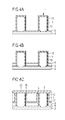
- FIG. 4C shows a correspondingly produced optoelectronic semiconductor chip in a schematic sectional illustration.
- the current spreading layer 13 is not applied directly to the mask layer 5 ; rather, before the current spreading layer 13 is applied, the stumps of the active regions 1 are passivated with an insulation material 4 .
- the insulation material 4 can be applied by a spin coating process, for example.
- the active regions 1 project beyond the insulation material 4 in the direction of the main extension direction R (in this respect, see, e.g., FIG. 4B ).
- the further processing takes place, for example, as described in connection with FIGS. 1B to 1G .
- the passivation at the stump leads to an optoelectronic semiconductor chip in which the probability of the occurrence of leakage currents is reduced.
Landscapes
- Led Devices (AREA)
Applications Claiming Priority (4)
| Application Number | Priority Date | Filing Date | Title |
|---|---|---|---|
| DE102012101718.2 | 2012-03-01 | ||
| DE102012101718.2A DE102012101718B4 (de) | 2012-03-01 | 2012-03-01 | Optoelektronischer Halbleiterchip |
| DE102012101718 | 2012-03-01 | ||
| PCT/EP2013/053371 WO2013127672A1 (de) | 2012-03-01 | 2013-02-20 | Optoelektronischer halbleiterchip |
Publications (2)
| Publication Number | Publication Date |
|---|---|
| US20150021636A1 US20150021636A1 (en) | 2015-01-22 |
| US9214600B2 true US9214600B2 (en) | 2015-12-15 |
Family
ID=47845931
Family Applications (1)
| Application Number | Title | Priority Date | Filing Date |
|---|---|---|---|
| US14/382,286 Active US9214600B2 (en) | 2012-03-01 | 2013-02-20 | Optoelectronic semiconductor chip |
Country Status (7)
| Country | Link |
|---|---|
| US (1) | US9214600B2 (de) |
| EP (1) | EP2820684A1 (de) |
| JP (1) | JP5952922B2 (de) |
| KR (1) | KR20150044422A (de) |
| CN (1) | CN104145346B (de) |
| DE (1) | DE102012101718B4 (de) |
| WO (1) | WO2013127672A1 (de) |
Cited By (2)
| Publication number | Priority date | Publication date | Assignee | Title |
|---|---|---|---|---|
| WO2017205123A1 (en) * | 2016-05-23 | 2017-11-30 | Microsoft Technology Licensing, Llc | Device having display integrated visible and infrared light source for user authentication |
| US11069835B2 (en) | 2017-03-20 | 2021-07-20 | Osram Oled Gmbh | Optoelectronic semiconductor chip and method of manufacturing the same |
Families Citing this family (21)
| Publication number | Priority date | Publication date | Assignee | Title |
|---|---|---|---|---|
| DE102012109594A1 (de) | 2012-10-09 | 2014-04-10 | Osram Opto Semiconductors Gmbh | Verfahren zur Herstellung eines optoelektronischen Halbleiterbauteils und optoelektronisches Halbleiterbauteil |
| DE102013114466A1 (de) | 2013-12-19 | 2015-06-25 | Osram Gmbh | Optoelektronisches Halbleiterbauteil und Verfahren zur Herstellung eines optoelektronischen Halbleiterbauteils |
| DE102014117995A1 (de) * | 2014-12-05 | 2016-06-09 | Osram Opto Semiconductors Gmbh | Halbleiterschichtenfolge zur Erzeugung von sichtbarem Licht und Leuchtdiode |
| DE102015120778B4 (de) | 2015-11-30 | 2021-09-23 | OSRAM Opto Semiconductors Gesellschaft mit beschränkter Haftung | Optoelektronisches Bauelement und Verfahren zur Herstellung eines optoelektronischen Bauelements |
| DE102015121554B4 (de) * | 2015-12-10 | 2022-01-13 | OSRAM Opto Semiconductors Gesellschaft mit beschränkter Haftung | Verfahren zur Herstellung von optoelektronischen Halbleiterchips und optoelektronischer Halbleiterchip |
| DE102016102876A1 (de) * | 2016-02-18 | 2017-08-24 | Osram Opto Semiconductors Gmbh | Optoelektronisches Halbleiterbauelement und Verfahren zur Herstellung eines optoelektronischen Halbleiterbauelements |
| DE102016114992A1 (de) * | 2016-08-12 | 2018-02-15 | Osram Opto Semiconductors Gmbh | Optoelektronischer Halbleiterchip |
| WO2018062252A1 (ja) | 2016-09-29 | 2018-04-05 | 日亜化学工業株式会社 | 発光素子 |
| DE102017113741A1 (de) | 2017-06-21 | 2018-12-27 | Osram Opto Semiconductors Gmbh | Optoelektronisches Halbleiterbauelement |
| DE102017113745A1 (de) * | 2017-06-21 | 2018-12-27 | Osram Opto Semiconductors Gmbh | Halbleiterdisplay, optoelektronisches Halbleiterbauteil und Verfahren zur Herstellung solcher |
| CN107749437A (zh) * | 2017-11-17 | 2018-03-02 | 广州市香港科大霍英东研究院 | 可挠性发光二极管制程及其结构 |
| EP3531459A1 (de) | 2018-02-23 | 2019-08-28 | Forschungsverbund Berlin e.V. | Halbleiterbauelement mit mindestens einem funktionselement mit mehreren aktiven bereichen und verfahren zu seiner herstellung |
| WO2020011117A1 (zh) * | 2018-07-12 | 2020-01-16 | 江西兆驰半导体有限公司 | 一种提高光提取效率的紫外发光二极管芯片及其制作方法 |
| JP7227463B2 (ja) * | 2018-12-27 | 2023-02-22 | 日亜化学工業株式会社 | 発光素子及びその製造方法 |
| CN110487685B (zh) * | 2019-08-29 | 2021-10-08 | 哈尔滨工业大学 | 一种沥青混合料骨架填充体系的评价方法 |
| US11462659B2 (en) | 2019-09-10 | 2022-10-04 | Koito Manufacturing Co., Ltd. | Semiconductor light emitting device and manufacturing method of semiconductor light emitting device |
| JP7336767B2 (ja) * | 2019-10-03 | 2023-09-01 | 株式会社小糸製作所 | 半導体発光素子および半導体発光素子の製造方法 |
| KR102902635B1 (ko) * | 2020-02-04 | 2025-12-23 | 삼성전자주식회사 | 3차원 구조 반도체 발광소자 및 디스플레이 장치 |
| GB2592208B (en) * | 2020-02-19 | 2022-04-06 | Plessey Semiconductors Ltd | High resolution monolithic RGB arrays |
| WO2024084634A1 (ja) * | 2022-10-19 | 2024-04-25 | 京セラ株式会社 | 半導体基板、半導体基板の製造方法および製造装置 |
| CN118712294B (zh) * | 2024-08-29 | 2024-11-15 | 山东省科学院激光研究所 | 一种纳米发光二极管及其制备方法 |
Citations (23)
| Publication number | Priority date | Publication date | Assignee | Title |
|---|---|---|---|---|
| JPH10173226A (ja) | 1996-12-06 | 1998-06-26 | Rohm Co Ltd | 半導体発光素子 |
| JPH10321910A (ja) | 1997-05-16 | 1998-12-04 | Ricoh Co Ltd | 半導体発光素子 |
| JP2002016312A (ja) | 2000-06-27 | 2002-01-18 | Sanyo Electric Co Ltd | 窒化物系半導体素子およびその製造方法 |
| US20050179052A1 (en) * | 2004-02-12 | 2005-08-18 | Yi Gyu C. | Heterojunction structure of nitride semiconductor and nano-device or an array thereof comprising same |
| EP1727216A2 (de) | 2005-05-24 | 2006-11-29 | LG Electronics, Inc. | Stabartige lichtemittierende Vorrichtung und Verfahren zu deren Herstellung |
| US20080157057A1 (en) * | 2005-06-25 | 2008-07-03 | Seoul Opto Device Co., Ltd | Nanostructure Having a Nitride-Based Quantum Well and Light Emitting Diode Employing the Same |
| JP2008282966A (ja) | 2007-05-10 | 2008-11-20 | Sony Corp | 半導体素子およびその製造方法 |
| WO2009009612A2 (en) | 2007-07-09 | 2009-01-15 | Nanocrystal, Llc | Growth of self-assembled gan nanowires and application in nitride semiconductor bulk material |
| US20090090900A1 (en) | 2005-07-29 | 2009-04-09 | Osram Opto Semiconductors Gmbh | Optoelectronic Semiconductor Chip |
| US7521274B2 (en) | 2006-03-10 | 2009-04-21 | Stc.Unm | Pulsed growth of catalyst-free growth of GaN nanowires and application in group III nitride semiconductor bulk material |
| US20100155767A1 (en) | 2008-12-23 | 2010-06-24 | Samsung Electronics Co., Ltd. | Light emitting device using a micro-rod and method of manufacturing a light emitting device |
| US20110012167A1 (en) | 2008-03-05 | 2011-01-20 | Takayuki Shimamura | Light emitting element |
| US20110095260A1 (en) * | 2009-10-28 | 2011-04-28 | Samsung Electronics Co., Ltd. | Light emitting device |
| WO2011067872A1 (ja) | 2009-12-01 | 2011-06-09 | 国立大学法人北海道大学 | 発光素子およびその製造方法 |
| US20110140072A1 (en) | 2008-08-21 | 2011-06-16 | Nanocrystal Corporation | Defect-free group iii - nitride nanostructures and devices using pulsed and non-pulsed growth techniques |
| US20110147702A1 (en) * | 2009-12-16 | 2011-06-23 | Lehigh University | Nitride based quantum well light-emitting devices having improved current injection efficiency |
| DE102009056712A1 (de) | 2009-12-04 | 2011-06-30 | Technische Universität Carolo-Wilhelmina zu Braunschweig, 38106 | Elektrische Anschlusselemente auf Nanosäulen |
| DE102010012711A1 (de) | 2010-03-25 | 2011-09-29 | Osram Opto Semiconductors Gmbh | Strahlungsemittierendes Halbleiterbauelement und Verfahren zur Herstellung eines strahlungsemittierenden Halbleiterbauelements |
| US20110240959A1 (en) | 2008-12-19 | 2011-10-06 | Glo Ab | Nanostructured device |
| US20120025232A1 (en) * | 2010-07-29 | 2012-02-02 | National Tsing Hua University | Iii-nitride light-emitting diode and method of producing the same |
| US20120061646A1 (en) * | 2009-05-22 | 2012-03-15 | Sun R&Db Foundation | Light emission device and manufacturing method thereof |
| US20120097920A1 (en) * | 2010-07-29 | 2012-04-26 | Shang-Jr Gwo | Iii-nitride light-emitting diode and method of producing the same |
| US20140117307A1 (en) * | 2012-10-26 | 2014-05-01 | Glo Ab | Nanowire Sized Opto-Electronic Structure and Method for Modifying Selected Portions of Same |
Family Cites Families (6)
| Publication number | Priority date | Publication date | Assignee | Title |
|---|---|---|---|---|
| JP2002261327A (ja) * | 2001-03-06 | 2002-09-13 | Sony Corp | 半導体発光素子及び半導体発光素子の製造方法 |
| CN101443887B (zh) * | 2006-03-10 | 2011-04-20 | Stc.Unm公司 | Gan纳米线的脉冲式生长及在族ⅲ氮化物半导体衬底材料中的应用和器件 |
| JP5453105B2 (ja) * | 2006-12-22 | 2014-03-26 | クナノ アーベー | ナノ構造のled及びデバイス |
| DE102009060750B4 (de) * | 2009-12-30 | 2025-04-10 | OSRAM Opto Semiconductors Gesellschaft mit beschränkter Haftung | Optoelektronischer Halbleiterchip und Verfahren zu dessen Herstellung |
| US20110240099A1 (en) * | 2010-03-30 | 2011-10-06 | Ellinger Carolyn R | Photovoltaic nanowire device |
| EP2583317A4 (de) * | 2010-06-18 | 2016-06-15 | Glo Ab | Nanodraht-led-struktur und verfahren zu ihrer herstellung |
-
2012
- 2012-03-01 DE DE102012101718.2A patent/DE102012101718B4/de active Active
-
2013
- 2013-02-20 US US14/382,286 patent/US9214600B2/en active Active
- 2013-02-20 JP JP2014559148A patent/JP5952922B2/ja active Active
- 2013-02-20 CN CN201380012011.5A patent/CN104145346B/zh active Active
- 2013-02-20 WO PCT/EP2013/053371 patent/WO2013127672A1/de not_active Ceased
- 2013-02-20 KR KR20147027327A patent/KR20150044422A/ko not_active Abandoned
- 2013-02-20 EP EP13708711.0A patent/EP2820684A1/de not_active Withdrawn
Patent Citations (31)
| Publication number | Priority date | Publication date | Assignee | Title |
|---|---|---|---|---|
| JPH10173226A (ja) | 1996-12-06 | 1998-06-26 | Rohm Co Ltd | 半導体発光素子 |
| JPH10321910A (ja) | 1997-05-16 | 1998-12-04 | Ricoh Co Ltd | 半導体発光素子 |
| JP2002016312A (ja) | 2000-06-27 | 2002-01-18 | Sanyo Electric Co Ltd | 窒化物系半導体素子およびその製造方法 |
| US20050179052A1 (en) * | 2004-02-12 | 2005-08-18 | Yi Gyu C. | Heterojunction structure of nitride semiconductor and nano-device or an array thereof comprising same |
| US20070041214A1 (en) | 2005-05-24 | 2007-02-22 | Ha Jun S | Rod type light emitting device and method for fabricating the same |
| JP2006332650A (ja) | 2005-05-24 | 2006-12-07 | Lg Electronics Inc | ロッド型発光素子及びその製造方法 |
| US8653538B2 (en) | 2005-05-24 | 2014-02-18 | Lg Electronics Inc. | Rod type light emitting device and method for fabricating the same |
| EP1727216A2 (de) | 2005-05-24 | 2006-11-29 | LG Electronics, Inc. | Stabartige lichtemittierende Vorrichtung und Verfahren zu deren Herstellung |
| US8330173B2 (en) * | 2005-06-25 | 2012-12-11 | Seoul Opto Device Co., Ltd. | Nanostructure having a nitride-based quantum well and light emitting diode employing the same |
| US20080157057A1 (en) * | 2005-06-25 | 2008-07-03 | Seoul Opto Device Co., Ltd | Nanostructure Having a Nitride-Based Quantum Well and Light Emitting Diode Employing the Same |
| US20090090900A1 (en) | 2005-07-29 | 2009-04-09 | Osram Opto Semiconductors Gmbh | Optoelectronic Semiconductor Chip |
| US7521274B2 (en) | 2006-03-10 | 2009-04-21 | Stc.Unm | Pulsed growth of catalyst-free growth of GaN nanowires and application in group III nitride semiconductor bulk material |
| JP2009542560A (ja) | 2006-03-10 | 2009-12-03 | エステイーシー.ユーエヌエム | III族窒化物半導体基板材料及びデバイスにおけるGaNナノワイヤーのパルス状成長及び応用 |
| JP2008282966A (ja) | 2007-05-10 | 2008-11-20 | Sony Corp | 半導体素子およびその製造方法 |
| WO2009009612A2 (en) | 2007-07-09 | 2009-01-15 | Nanocrystal, Llc | Growth of self-assembled gan nanowires and application in nitride semiconductor bulk material |
| US20110012167A1 (en) | 2008-03-05 | 2011-01-20 | Takayuki Shimamura | Light emitting element |
| US20110140072A1 (en) | 2008-08-21 | 2011-06-16 | Nanocrystal Corporation | Defect-free group iii - nitride nanostructures and devices using pulsed and non-pulsed growth techniques |
| US20110240959A1 (en) | 2008-12-19 | 2011-10-06 | Glo Ab | Nanostructured device |
| US20100155767A1 (en) | 2008-12-23 | 2010-06-24 | Samsung Electronics Co., Ltd. | Light emitting device using a micro-rod and method of manufacturing a light emitting device |
| US8878231B2 (en) * | 2009-05-22 | 2014-11-04 | Snu R&Db Foundation | Light emission device and manufacturing method thereof |
| US20120061646A1 (en) * | 2009-05-22 | 2012-03-15 | Sun R&Db Foundation | Light emission device and manufacturing method thereof |
| US20110095260A1 (en) * | 2009-10-28 | 2011-04-28 | Samsung Electronics Co., Ltd. | Light emitting device |
| US8895958B2 (en) | 2009-12-01 | 2014-11-25 | National University Corporation Hokkaido University | Light emitting element and method for manufacturing same |
| WO2011067872A1 (ja) | 2009-12-01 | 2011-06-09 | 国立大学法人北海道大学 | 発光素子およびその製造方法 |
| DE102009056712A1 (de) | 2009-12-04 | 2011-06-30 | Technische Universität Carolo-Wilhelmina zu Braunschweig, 38106 | Elektrische Anschlusselemente auf Nanosäulen |
| US20110147702A1 (en) * | 2009-12-16 | 2011-06-23 | Lehigh University | Nitride based quantum well light-emitting devices having improved current injection efficiency |
| US8907321B2 (en) * | 2009-12-16 | 2014-12-09 | Lehigh Univeristy | Nitride based quantum well light-emitting devices having improved current injection efficiency |
| DE102010012711A1 (de) | 2010-03-25 | 2011-09-29 | Osram Opto Semiconductors Gmbh | Strahlungsemittierendes Halbleiterbauelement und Verfahren zur Herstellung eines strahlungsemittierenden Halbleiterbauelements |
| US20120097920A1 (en) * | 2010-07-29 | 2012-04-26 | Shang-Jr Gwo | Iii-nitride light-emitting diode and method of producing the same |
| US20120025232A1 (en) * | 2010-07-29 | 2012-02-02 | National Tsing Hua University | Iii-nitride light-emitting diode and method of producing the same |
| US20140117307A1 (en) * | 2012-10-26 | 2014-05-01 | Glo Ab | Nanowire Sized Opto-Electronic Structure and Method for Modifying Selected Portions of Same |
Cited By (4)
| Publication number | Priority date | Publication date | Assignee | Title |
|---|---|---|---|---|
| WO2017205123A1 (en) * | 2016-05-23 | 2017-11-30 | Microsoft Technology Licensing, Llc | Device having display integrated visible and infrared light source for user authentication |
| CN109154741A (zh) * | 2016-05-23 | 2019-01-04 | 微软技术许可有限责任公司 | 具有用于用户认证的显示器集成的可见和红外光源的设备 |
| US11416041B2 (en) | 2016-05-23 | 2022-08-16 | Microsoft Technology Licensing, Llc. | Device having display integrated infrared and visible light source |
| US11069835B2 (en) | 2017-03-20 | 2021-07-20 | Osram Oled Gmbh | Optoelectronic semiconductor chip and method of manufacturing the same |
Also Published As
| Publication number | Publication date |
|---|---|
| US20150021636A1 (en) | 2015-01-22 |
| DE102012101718B4 (de) | 2025-08-28 |
| JP5952922B2 (ja) | 2016-07-13 |
| KR20150044422A (ko) | 2015-04-24 |
| JP2015508941A (ja) | 2015-03-23 |
| CN104145346B (zh) | 2017-05-10 |
| DE102012101718A1 (de) | 2013-09-05 |
| CN104145346A (zh) | 2014-11-12 |
| EP2820684A1 (de) | 2015-01-07 |
| WO2013127672A1 (de) | 2013-09-06 |
Similar Documents
| Publication | Publication Date | Title |
|---|---|---|
| US9214600B2 (en) | Optoelectronic semiconductor chip | |
| US9735319B2 (en) | Radiation emitting or receiving optoelectronic semiconductor chip | |
| CN108963051B (zh) | 发光二极管封装件 | |
| US8866175B2 (en) | Optoelectronic semiconductor chip | |
| US10181547B2 (en) | Optoelectronic semiconductor chip and method for producing optoelectronic semiconductor chips | |
| JP2006108698A (ja) | フリップチップ発光デバイス用のコンタクト及び全方向反射ミラー | |
| US8860063B2 (en) | Light-emitting diode chip | |
| US8952395B2 (en) | Wafer-level solid state transducer packaging transducers including separators and associated systems and methods | |
| CN103325907A (zh) | 具凹槽电极与光提取结构的发光二极管晶粒及其制作方法 | |
| US9530935B2 (en) | Method for fabricating a plurality of opto-electronic semiconductor chips, and opto-electronic semiconductor chip | |
| KR100969127B1 (ko) | 발광 소자, 발광 소자 제조방법 및 발광 소자 패키지 | |
| US20130062657A1 (en) | Light emitting diode structure and manufacturing method thereof | |
| US8592242B2 (en) | Etching growth layers of light emitting devices to reduce leakage current | |
| US9711679B2 (en) | Front-side emitting mid-infrared light emitting diode fabrication methods | |
| JP6697020B2 (ja) | 窒素及びリンを含有する発光層を有する発光ダイオード | |
| KR20060134490A (ko) | 플립 칩 질화물반도체 발광 다이오드 및 그의 제조 방법 | |
| KR101750207B1 (ko) | 발광 소자 및 발광 소자 패키지 | |
| KR101643410B1 (ko) | 발광 소자, 발광 소자 제조방법 및 발광 소자 패키지 | |
| US20190013434A1 (en) | Method for Manufacturing an Optoelectronic Component, and Optoelectronic Component | |
| KR20150144123A (ko) | 발광 소자 및 그 제조방법 | |
| KR20130110380A (ko) | 반도체 발광소자 및 그 제조방법 |
Legal Events
| Date | Code | Title | Description |
|---|---|---|---|
| AS | Assignment |
Owner name: OSRAM OPTO SEMICONDUCTORS GMBH, GERMANY Free format text: ASSIGNMENT OF ASSIGNORS INTEREST;ASSIGNORS:MANDL, MARTIN;STRASSBURG, MARTIN;KOELPER, CHRISTOPHER;AND OTHERS;SIGNING DATES FROM 20141107 TO 20141124;REEL/FRAME:034398/0662 |
|
| STCF | Information on status: patent grant |
Free format text: PATENTED CASE |
|
| MAFP | Maintenance fee payment |
Free format text: PAYMENT OF MAINTENANCE FEE, 4TH YEAR, LARGE ENTITY (ORIGINAL EVENT CODE: M1551); ENTITY STATUS OF PATENT OWNER: LARGE ENTITY Year of fee payment: 4 |
|
| AS | Assignment |
Owner name: OSRAM OLED GMBH, GERMANY Free format text: ASSIGNMENT OF ASSIGNORS INTEREST;ASSIGNOR:OSRAM OPTO SEMICONDUCTORS GMBH;REEL/FRAME:051467/0906 Effective date: 20191218 |
|
| MAFP | Maintenance fee payment |
Free format text: PAYMENT OF MAINTENANCE FEE, 8TH YEAR, LARGE ENTITY (ORIGINAL EVENT CODE: M1552); ENTITY STATUS OF PATENT OWNER: LARGE ENTITY Year of fee payment: 8 |