US9113564B2 - Circuit board - Google Patents
Circuit board Download PDFInfo
- Publication number
- US9113564B2 US9113564B2 US13/717,901 US201213717901A US9113564B2 US 9113564 B2 US9113564 B2 US 9113564B2 US 201213717901 A US201213717901 A US 201213717901A US 9113564 B2 US9113564 B2 US 9113564B2
- Authority
- US
- United States
- Prior art keywords
- distal end
- land
- end side
- connection terminal
- side continuous
- Prior art date
- Legal status (The legal status is an assumption and is not a legal conclusion. Google has not performed a legal analysis and makes no representation as to the accuracy of the status listed.)
- Active, expires
Links
Images


Classifications
-
- H—ELECTRICITY
- H05—ELECTRIC TECHNIQUES NOT OTHERWISE PROVIDED FOR
- H05K—PRINTED CIRCUITS; CASINGS OR CONSTRUCTIONAL DETAILS OF ELECTRIC APPARATUS; MANUFACTURE OF ASSEMBLAGES OF ELECTRICAL COMPONENTS
- H05K1/00—Printed circuits
- H05K1/18—Printed circuits structurally associated with non-printed electric components
-
- H—ELECTRICITY
- H05—ELECTRIC TECHNIQUES NOT OTHERWISE PROVIDED FOR
- H05K—PRINTED CIRCUITS; CASINGS OR CONSTRUCTIONAL DETAILS OF ELECTRIC APPARATUS; MANUFACTURE OF ASSEMBLAGES OF ELECTRICAL COMPONENTS
- H05K1/00—Printed circuits
- H05K1/02—Details
- H05K1/11—Printed elements for providing electric connections to or between printed circuits
- H05K1/111—Pads for surface mounting, e.g. lay-out
-
- H—ELECTRICITY
- H05—ELECTRIC TECHNIQUES NOT OTHERWISE PROVIDED FOR
- H05K—PRINTED CIRCUITS; CASINGS OR CONSTRUCTIONAL DETAILS OF ELECTRIC APPARATUS; MANUFACTURE OF ASSEMBLAGES OF ELECTRICAL COMPONENTS
- H05K3/00—Apparatus or processes for manufacturing printed circuits
- H05K3/30—Assembling printed circuits with electric components, e.g. with resistor
- H05K3/32—Assembling printed circuits with electric components, e.g. with resistor electrically connecting electric components or wires to printed circuits
- H05K3/34—Assembling printed circuits with electric components, e.g. with resistor electrically connecting electric components or wires to printed circuits by soldering
-
- H—ELECTRICITY
- H05—ELECTRIC TECHNIQUES NOT OTHERWISE PROVIDED FOR
- H05K—PRINTED CIRCUITS; CASINGS OR CONSTRUCTIONAL DETAILS OF ELECTRIC APPARATUS; MANUFACTURE OF ASSEMBLAGES OF ELECTRICAL COMPONENTS
- H05K1/00—Printed circuits
- H05K1/02—Details
- H05K1/0266—Marks, test patterns or identification means
- H05K1/0269—Marks, test patterns or identification means for visual or optical inspection
-
- H—ELECTRICITY
- H05—ELECTRIC TECHNIQUES NOT OTHERWISE PROVIDED FOR
- H05K—PRINTED CIRCUITS; CASINGS OR CONSTRUCTIONAL DETAILS OF ELECTRIC APPARATUS; MANUFACTURE OF ASSEMBLAGES OF ELECTRICAL COMPONENTS
- H05K2201/00—Indexing scheme relating to printed circuits covered by H05K1/00
- H05K2201/09—Shape and layout
- H05K2201/09209—Shape and layout details of conductors
- H05K2201/09372—Pads and lands
- H05K2201/09381—Shape of non-curved single flat metallic pad, land or exposed part thereof; Shape of electrode of leadless component
-
- H—ELECTRICITY
- H05—ELECTRIC TECHNIQUES NOT OTHERWISE PROVIDED FOR
- H05K—PRINTED CIRCUITS; CASINGS OR CONSTRUCTIONAL DETAILS OF ELECTRIC APPARATUS; MANUFACTURE OF ASSEMBLAGES OF ELECTRICAL COMPONENTS
- H05K2201/00—Indexing scheme relating to printed circuits covered by H05K1/00
- H05K2201/09—Shape and layout
- H05K2201/09818—Shape or layout details not covered by a single group of H05K2201/09009 - H05K2201/09809
- H05K2201/099—Coating over pads, e.g. solder resist partly over pads
-
- H—ELECTRICITY
- H05—ELECTRIC TECHNIQUES NOT OTHERWISE PROVIDED FOR
- H05K—PRINTED CIRCUITS; CASINGS OR CONSTRUCTIONAL DETAILS OF ELECTRIC APPARATUS; MANUFACTURE OF ASSEMBLAGES OF ELECTRICAL COMPONENTS
- H05K3/00—Apparatus or processes for manufacturing printed circuits
- H05K3/30—Assembling printed circuits with electric components, e.g. with resistor
- H05K3/32—Assembling printed circuits with electric components, e.g. with resistor electrically connecting electric components or wires to printed circuits
- H05K3/34—Assembling printed circuits with electric components, e.g. with resistor electrically connecting electric components or wires to printed circuits by soldering
- H05K3/341—Surface mounted components
- H05K3/3421—Leaded components
-
- Y—GENERAL TAGGING OF NEW TECHNOLOGICAL DEVELOPMENTS; GENERAL TAGGING OF CROSS-SECTIONAL TECHNOLOGIES SPANNING OVER SEVERAL SECTIONS OF THE IPC; TECHNICAL SUBJECTS COVERED BY FORMER USPC CROSS-REFERENCE ART COLLECTIONS [XRACs] AND DIGESTS
- Y02—TECHNOLOGIES OR APPLICATIONS FOR MITIGATION OR ADAPTATION AGAINST CLIMATE CHANGE
- Y02P—CLIMATE CHANGE MITIGATION TECHNOLOGIES IN THE PRODUCTION OR PROCESSING OF GOODS
- Y02P70/00—Climate change mitigation technologies in the production process for final industrial or consumer products
- Y02P70/50—Manufacturing or production processes characterised by the final manufactured product
Definitions
- the present disclosure relates to a circuit board. More particularly, the present disclosure relates to the field of improving the accuracy of detecting whether a solder joint of a connection terminal to a land is successful or not, by providing a narrow portion which is narrower than other portions.
- the land is used to join a distal end portion of the connection terminal of a lead component by soldering.
- a variety of kinds of electronic devices such as a television receiver, personal computer, and audio equipment include a circuit board disposed therein.
- the circuit board may include a wiring plate on which a circuit pattern is formed on an insulation substrate using a copper foil and a plurality of electronic parts mounted on the circuit pattern of the wiring plate.
- a lead component such as a QFP (Quad Flat Package) or a connector may be used as electronic parts.
- the lead component includes a main body formed of ceramic and other material, and a plurality of connection terminals protruding from each side of the main body. Each of the connection terminals is joined to each corresponding land of the circuit pattern by soldering (for example, see FIG. 6 in Japanese Patent Application Laid-Open Publication No. 2003-10216).
- the lead component is a component in which the quality of electronic devices in the market is greatly affected by thermal deformation behavior and the quality in the initial stage.
- the lead component is necessary to ensure the high quality of circuit board in a mounting process.
- an inspection device inspects whether a solder joint of the connection terminal to the land is successful or not.
- the inspection of whether the solder joint is successful or not is performed by two- or three-dimensional image detection or the like.
- soldered portion at a distal end side of the connection terminal from among the solders (solder fillets) applied to the lands, and the light is irradiated in a direction perpendicular or oblique to the soldered portion. Then, the determination of whether the solder joint is successful or not is made based on the difference in the shape or luminance level of the portion irradiated with light.
- a float amount indicating how far away the connection terminal is from the land is detected, and then the determination of whether the solder joint is successful or not is made based on the float amount of the connection terminal with respect to the land.
- a land is formed in a rectangular shape.
- the determination of whether the solder joint is successful or not is made based on the float amount of the connection terminal b with respect to the land d.
- each of FIG. 12C and FIG. 12D shows a good solder joint and FIG. 12E shows a bad solder joint.
- a state of FIG. 12D having a good solder joint is likely to be determined to be a solder joint failure because it has exceeded a threshold H.
- a state of FIG. 12E having a bad solder joint is likely to be determined to be a solder joint success because it has not exceeded the threshold H.
- an embodiment of the present disclosure is made to overcome the above problem, and provides a circuit board capable of improving accuracy of detecting whether a solder joint of a connection terminal to a land is successful or not.
- a circuit board includes a land and a narrow portion.
- the land is provided on a mounting surface and used as a portion to which a distal end portion of a connection terminal of a lead component is joined by a solder.
- the land is formed to extend to a predetermined direction such that the predetermined direction is a longitudinal direction of the land and a lateral direction orthogonal to the longitudinal direction is a width direction of the land.
- the land includes a terminal-facing portion facing the distal end portion of the connection terminal and a distal end side continuous portion continuously extending from the terminal-facing portion in the distal end portion of the connection terminal.
- the narrow portion is provided in the terminal-facing portion.
- the narrow portion has a width smaller than a width of the distal end side continuous portion.
- the narrow portion is preferably formed to include a recessed portion formed at one side of the narrow portion in the width direction, and the recessed portion is preferably opened in the width direction.
- the narrow portion is formed to include a recessed portion formed at one side of the narrow portion in the width direction and the recessed portion is opened in the width direction, thereby ensuring good workability of the land.
- the narrow portion is preferably formed to include a recessed portion formed at both sides respectively of the narrow portion in the width direction, and the recessed portion is preferably opened in the width direction.
- the narrow portion is preferably formed to include a recessed portion formed at both sides respectively of the narrow portion in the width direction and the recessed portion is opened in the width direction, it is possible to ensure good workability of the land.
- the distal end side continuous portion preferably has a width greater than a width of the connection terminal, and the narrow portion preferably has a width smaller than the width of the connection terminal.
- the distal end side continuous portion has a width greater than a width of the connection terminal and the narrow portion has a width smaller than the width of the connection terminal, thereby ensuring an amount of the solder sufficient to be applied to the distal end side continuous portion.
- the distal end side continuous portion preferably has a length greater than that of the narrow portion.
- the configuration of the distal end side continuous portion having a length greater than the length of the narrow portion makes it possible to ensure a length of the distal end side continuous portion necessary to perform an inspection, even when the positional accuracy of the lead component with respect to the land at the time of mounting or the position detection accuracy of the inspection device with respect to the land is lowered.
- the land is preferably provided to include a proximal end side continuous portion continuously extending from the terminal-facing portion on the opposite side of the distal end side continuous portion such that the terminal-facing portion is disposed between the proximal end side continuous portion and the distal end side continuous portion.
- the land is provided to include a proximal end side continuous portion continuously extending from the terminal-facing portion on the opposite side of the distal end side continuous portion such that the terminal-facing portion is disposed between the proximal end side continuous portion and the distal end side continuous portion, it is possible for the proximal end side continuous portion to be adhered closely to the connection terminal applied by the solder.
- the circuit board includes a land provided on a mounting surface for joining a distal end portion of a connection terminal of a lead component by a solder.
- the land is formed to extend in a predetermined direction such that the predetermined direction is a longitudinal direction and a lateral direction orthogonal to the longitudinal direction is a width direction.
- the land is provided with a terminal-facing portion facing the distal end portion of the connection terminal and a distal end side continuous portion continuously extending from the terminal-facing portion in the distal end portion of the connection terminal.
- the land includes a narrow portion having a width smaller than a width of the distal end side continuous portion in the terminal-facing portion.
- the narrow portion has a recessed portion formed at one side thereof in the width direction, and the recessed portion is opened in the width direction.
- the narrow portion can be formed easily while ensuring better workability of the land.
- the narrow portion has recessed portions formed at both sides thereof in the width direction and the recessed portions is opened in the width direction.
- the narrow portion can be formed easily while ensuring better workability of the land.
- the distal end side continuous portion has a width greater than a width of the connection terminal, and the narrow portion has a width smaller than the width of the connection terminal.
- the narrow portion can be formed on the land while ensuring a sufficient amount of the solder applied on the distal end side continuous portion and ensuring a good joining of the connection terminal to the land.
- the distal end side continuous portion has a length greater than a length of the narrow portion.
- the distal end side continuous portion has a sufficient length.
- the positional accuracy of the lead component with respect to the land at the time of mounting or the position detection accuracy of the inspection device with respect to the land is lowered, it is ensured that the accuracy of detecting whether the solder joint of the connection terminal to the land is successful or not, because the distal end side continuous portion has a length which is necessary to perform an inspection.
- the land includes a proximal end side continuous portion continuously extending from the terminal-facing portion on the opposite side of the distal end side continuous portion such that the terminal-facing portion is disposed between the proximal end side continuous portion and the distal end side continuous portion.
- the proximal end side continuous portion can be adhered closely to the connection terminal applied by the solder, thereby ensuring a good joining of the connection terminal to the land.
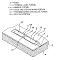
- FIG. 1 illustrates a best mode contemplated for practicing a circuit board according to embodiments of the present disclosure along with from FIG. 2 to FIG. 10 , and specifically is a partial enlarged perspective view showing the circuit board;
- FIG. 2 is a partial enlarged perspective view showing a wiring plate
- FIG. 3 is an enlarged plan view of a land
- FIG. 4 is a partial enlarged side view in cross-section showing a case where a connection terminal is joined to the land in a good soldering state
- FIG. 5 is a partial enlarged side view in cross-section showing a case where a solder joint failure of the connection terminal occurs
- FIG. 6 is an enlarged sectional view showing a state of the solder applied to a terminal-facing portion of the land
- FIG. 7 is an enlarged sectional view showing a state of the solder applied to a distal end side continuous portion of the land;
- FIG. 8 is a graph showing results obtained by detecting the luminance level of light when an inspection device inspects whether a solder joint is successful or not;
- FIG. 9 is an enlarged plan view showing another example of the land.
- FIG. 10 is an enlarged perspective view showing still another example of the land
- FIGS. 11A and 11B illustrate a joining state of a connection terminal in a circuit board according to related art, in which FIG. 11A is a partial enlarged side view in cross-section showing a state where the connection terminal is joined to a land in a good soldering state, and FIG. 11B is a partial enlarged side view in cross-section showing a state where the connection terminal is joined to the land in a bad soldering state; and
- FIGS. 12C to 12E illustrate another joining state of the connection terminal in the circuit board according to related art, in which FIGS. 12C and 12D are partial enlarged side views in cross-section showing a state where the connection terminal is joined to a land in a good soldering state, and FIG. 12E is a partial enlarged side view in cross-section showing a state where the connection terminal is joined to the land in a bad soldering state.
- a circuit board 1 has a wiring plate 2 and a plurality of electronic parts including a lead component 3 mounted on the wiring plate 2 (referring to FIG. 1 ).
- the wiring plate 2 has an insulating substrate 4 with a predetermined circuit pattern 5 formed thereon.
- the lead component 3 is mounted on a plurality of lands 6 formed on a distal end portion of the circuit pattern 5 .
- Examples of the insulating substrate 4 include a glass epoxy substrate, a paper phenol substrate, a paper epoxy substrate, a glass composite substrate, and other substrate.
- the circuit pattern 5 is formed with a copper foil having a thickness on the order of several tens of micrometers ( ⁇ m).
- the lead component 3 has a main body 7 and a plurality of connection terminals 8 protruding outward from an outer circumference surface of the main body 7 .
- the connection terminal 8 has a base portion 8 a protruding laterally from the main body 7 , an intermediate portion 8 b bent in the direction perpendicular to the base portion 8 a , and a joining portion 8 c bent in the direction perpendicular to the intermediate portion 8 b .
- the joining portion 8 c is a distal end portion of the connection terminal 8 and is a portion to be joined to the land 6 by soldering.
- the land 6 is formed as a part of a rectangular base material 9 extending in one direction (referring to FIG. 2 ). More specifically, a mask process is performed by applying a resist 10 on the wiring plate 2 , and a portion other than the outer circumference portion of the base material 9 covered with the resist 10 is provided as the land 6 .
- the terminal-facing portion 11 is a portion which faces the joining portion 8 c of the connection terminal 8 .
- the land 6 has a distal end side continuous portion 12 and a proximal end side continuous portion 13 .
- the distal end side continuous portion 12 is extended from the terminal-facing portion 11 at one end in the longitudinal direction
- the proximal end side continuous portion 13 is extended from the terminal-facing portion 11 at the other end in the longitudinal direction.
- An intermediate portion of the terminal-facing portion 11 in the longitudinal direction is formed as a narrow portion 11 a having a width (length in the lateral direction) smaller than other portions of the terminal-facing portion 11 .
- the narrow portion 11 a for example, has a recessed portion 14 at both sides respectively in the width direction. Each of the recessed portions is opened in the width direction (lateral direction).
- Portions other than the narrow portion 11 a of the terminal-facing portion 11 have a width greater than that of the connection terminal 8 and have the same width as the distal end side continuous portion 12 .
- the width of the narrow portion 11 a is smaller than or equal to the width of the connection terminal 8 .
- the distal end side continuous portion 12 has a length greater than that of the narrow portion 11 a of the terminal-facing portion 11 .
- the lead component 3 is mounted on the wiring plate 2 so that the joining portion 8 c of the connection terminal 8 is joined to the land 6 by a solder 15 (referring to FIG. 4 ).
- the solder 15 is adhered closely to each side of the joining portion 8 c .
- the outer surface of the solder 15 is formed into a gentle concave curved surface, resulting in forming a mountain shape, without depending on the shape of the land 6 .
- the solder 15 does not adhere closely to the joining portion 8 c , and is formed into a shape depending on the shape of the land 6 . More specifically, since the surface curvature of each of the solder 15 has the same cross-sectional shape in the lateral direction irrespective of position of the soldered portion in the longitudinal direction of the land 6 , the solder 15 has a low height as a portion of the land 6 applied with the solder 15 has a smaller width. Thus, the solder is formed to be lower at the narrow portion 11 a (referring to FIG. 6 ) and to be higher at the distal end side continuous portion 12 (referring to FIG. 7 ).
- an inspection device inspects whether the solder joint of the connection terminal to the land is successful.
- the inspection in the inspection device is performed by irradiating with light on a soldered portion at the distal end side of the connection terminal 8 from among the solders 15 (solder fillets) applied to the lands 6 , and the light is irradiated in a direction perpendicular or oblique to the soldered portion.
- the reflected light is incident on a light detection unit of the inspection device. Then, the light detection unit of the inspection device detects the luminance level of the incident light, thereby determining whether the solder joint of each of the connection terminals 8 is successful or not.
- the luminance level of light incident on the light detection unit is significantly different between the case where the joining portion 8 c is joined to the land 6 in a good soldering state and the case where the joining portion 8 c is joined to the land 6 in a bad soldering state.
- a distinction is made between the case where the joining portion 8 c is joined to the land 6 in a good soldering state and the case where the joining portion 8 c is joined to the land 6 in a bad soldering state, based on the luminance level of light incident on the light detection unit.
- FIG. 8 illustrates results obtained by detecting the luminance level of light when the inspection device inspects whether the solder joint is successful or not.
- the horizontal axis indicates the luminance level of light
- the vertical axis indicates the number of the detected connection terminals 8 .
- the narrow portion 11 a having a width smaller than that of the distal end side continuous portion 12 is provided in the terminal-facing portion 11 of the land 6 .
- the amount of the solder 15 applied on the narrow portion 11 a is reduced, accordingly, the amount of solder to be applied on the distal end side continuous portion 12 will be increased. Additionally, the shape of the solder 15 (solder fillet) on the distal end side continuous portion 12 is significantly different from each other depending on whether the solder joint is successful or not. As a result, it is possible to improve the accuracy of detecting whether the solder joint of the connection terminal 8 to the land 6 is successful or not.
- the narrow portion 11 a has a recessed portion 14 at both sides respectively in the width direction.
- the narrow portion 11 a can be formed easily while ensuring good workability of the land 6 .
- the narrow portion 11 a may have the recessed portion 14 on one side in the width direction. In this case, the narrow portion 11 a can be formed easily while ensuring better workability of the land 6 .
- the distal end side continuous portion 12 of the land 6 is formed to have a width greater than that of the connection terminal 8 .
- the narrow portion 11 a is formed to have a width smaller than or equal to the width of the connection terminal 8 .
- the narrow portion 11 a can be formed on the land 6 while ensuring a sufficient amount of the solder 15 applied on the distal end side continuous portion 12 and ensuring a good joining of the connection terminal 8 to the land 6 .
- distal end side continuous portion 12 has a length greater than the length of the narrow portion 11 a.
- the distal end side continuous portion 12 has a sufficient length.
- the positional accuracy of the lead component 3 with respect to the land 6 at the time of mounting or the position detection accuracy of the inspection device with respect to the land 6 is lowered, it is possible to improve the accuracy of detecting whether the solder joint of the connection terminal 8 to the land 6 is successful or not, because the distal end side continuous portion 12 has a length which is necessary to perform an inspection.
- the proximal end side continuous portion 13 extending from the terminal-facing portion 11 is formed on the land 6 at the opposite side of the distal end side continuous portion 12 such that the terminal-facing portion 11 is disposed between the distal end side continuous portion 12 and the proximal end side continuous portion 13 .
- the solder 15 is applied to the proximal end side continuous portion 13 as well, and thus the proximal end side continuous portion 13 is adhered closely to the connection terminal 8 , thereby ensuring a good solder joint of the connection terminal 8 with respect to the land 6 .
- present technology may also be configured as below.
- a circuit board including:
- the land is formed to extend in a predetermined direction such that the predetermined direction is a longitudinal direction and a lateral direction orthogonal to the longitudinal direction is a width direction,
- the land includes a terminal-facing portion facing the distal end portion of the connection terminal and a distal end side continuous portion continuously extending from the terminal-facing portion in the distal end portion of the connection terminal, and
- the land includes a narrow portion having a width smaller than a width of the distal end side continuous portion in the terminal-facing portion.
- distal end side continuous portion has a width greater than a width of the connection terminal
- the narrow portion has a width smaller than the width of the connection terminal.
Landscapes
- Engineering & Computer Science (AREA)
- Microelectronics & Electronic Packaging (AREA)
- Manufacturing & Machinery (AREA)
- Electric Connection Of Electric Components To Printed Circuits (AREA)
- Coupling Device And Connection With Printed Circuit (AREA)
Applications Claiming Priority (2)
| Application Number | Priority Date | Filing Date | Title |
|---|---|---|---|
| JP2012-030939 | 2012-02-15 | ||
| JP2012030939A JP6396633B2 (ja) | 2012-02-15 | 2012-02-15 | 回路基板 |
Publications (2)
| Publication Number | Publication Date |
|---|---|
| US20130206456A1 US20130206456A1 (en) | 2013-08-15 |
| US9113564B2 true US9113564B2 (en) | 2015-08-18 |
Family
ID=48944678
Family Applications (1)
| Application Number | Title | Priority Date | Filing Date |
|---|---|---|---|
| US13/717,901 Active 2033-09-19 US9113564B2 (en) | 2012-02-15 | 2012-12-18 | Circuit board |
Country Status (4)
| Country | Link |
|---|---|
| US (1) | US9113564B2 (enExample) |
| JP (1) | JP6396633B2 (enExample) |
| KR (1) | KR20130094235A (enExample) |
| CN (1) | CN103260346B (enExample) |
Cited By (1)
| Publication number | Priority date | Publication date | Assignee | Title |
|---|---|---|---|---|
| US20220399258A1 (en) * | 2021-06-09 | 2022-12-15 | Western Digital Technologies, Inc. | Substrate Bonding Pad Having a Multi-Surface Trace Interface |
Families Citing this family (5)
| Publication number | Priority date | Publication date | Assignee | Title |
|---|---|---|---|---|
| CN105828521B (zh) * | 2015-01-08 | 2018-10-02 | 上海和辉光电有限公司 | 印刷电路板的布局方法及印刷电路板 |
| US11195269B2 (en) * | 2015-03-27 | 2021-12-07 | Texas Instruments Incorporated | Exposed pad integrated circuit package |
| JP2016192352A (ja) * | 2015-03-31 | 2016-11-10 | 株式会社オートネットワーク技術研究所 | ワイヤーハーネス及びワイヤーハーネスの製造方法 |
| CN106455350A (zh) * | 2016-09-29 | 2017-02-22 | 广东小天才科技有限公司 | 一种元器件的更换方法 |
| US11839031B2 (en) | 2022-04-06 | 2023-12-05 | Western Digital Technologies, Inc. | Micro solder joint and stencil aperture design |
Citations (4)
| Publication number | Priority date | Publication date | Assignee | Title |
|---|---|---|---|---|
| US5303122A (en) * | 1991-10-31 | 1994-04-12 | Ford Motor Company | Printed circuit board having a commonized mounting pad which different sized surface mounted devices can be mounted |
| US5453582A (en) * | 1993-03-11 | 1995-09-26 | The Furukawa Electric Co., Ltd. | Circuit board to be precoated with solder layers and solder circuit board |
| US20100181102A1 (en) * | 2009-01-21 | 2010-07-22 | Fujitsu Limited | Printed circuit board and printed circuit board unit |
| US7995353B2 (en) * | 2008-04-22 | 2011-08-09 | Hon Hai Precision Industry Co., Ltd. | Circuit board and electronic device using the same |
Family Cites Families (9)
| Publication number | Priority date | Publication date | Assignee | Title |
|---|---|---|---|---|
| JPH04217388A (ja) * | 1990-12-19 | 1992-08-07 | Mitsubishi Electric Corp | 印刷配線板 |
| JPH0718475U (ja) * | 1993-09-09 | 1995-03-31 | 日本ビクター株式会社 | 印刷配線板 |
| JPH07106745A (ja) * | 1993-09-30 | 1995-04-21 | Ibiden Co Ltd | プリント配線板及びパッドへの半田皮膜形成方法 |
| KR100304649B1 (ko) * | 1999-02-02 | 2001-09-13 | 윤종용 | 집적회로 패키지의 리드핀 납땜 검사방법 및 검사장치 |
| JP3948376B2 (ja) * | 2002-09-05 | 2007-07-25 | 株式会社デンソー | 電子装置の製造方法 |
| JP2007281122A (ja) * | 2006-04-05 | 2007-10-25 | Denso Corp | モールドパッケージの実装構造 |
| JP2009141170A (ja) * | 2007-12-07 | 2009-06-25 | Fujitsu Component Ltd | 基板のパッド構造 |
| CN101656217B (zh) * | 2008-08-18 | 2011-03-23 | 中芯国际集成电路制造(上海)有限公司 | 系统级封装的方法 |
| CN102314009A (zh) * | 2011-09-09 | 2012-01-11 | 深圳市华星光电技术有限公司 | 液晶显示模组及液晶显示面板 |
-
2012
- 2012-02-15 JP JP2012030939A patent/JP6396633B2/ja active Active
- 2012-12-18 US US13/717,901 patent/US9113564B2/en active Active
-
2013
- 2013-02-07 KR KR1020130013731A patent/KR20130094235A/ko not_active Withdrawn
- 2013-02-08 CN CN201310050910.6A patent/CN103260346B/zh active Active
Patent Citations (4)
| Publication number | Priority date | Publication date | Assignee | Title |
|---|---|---|---|---|
| US5303122A (en) * | 1991-10-31 | 1994-04-12 | Ford Motor Company | Printed circuit board having a commonized mounting pad which different sized surface mounted devices can be mounted |
| US5453582A (en) * | 1993-03-11 | 1995-09-26 | The Furukawa Electric Co., Ltd. | Circuit board to be precoated with solder layers and solder circuit board |
| US7995353B2 (en) * | 2008-04-22 | 2011-08-09 | Hon Hai Precision Industry Co., Ltd. | Circuit board and electronic device using the same |
| US20100181102A1 (en) * | 2009-01-21 | 2010-07-22 | Fujitsu Limited | Printed circuit board and printed circuit board unit |
Cited By (2)
| Publication number | Priority date | Publication date | Assignee | Title |
|---|---|---|---|---|
| US20220399258A1 (en) * | 2021-06-09 | 2022-12-15 | Western Digital Technologies, Inc. | Substrate Bonding Pad Having a Multi-Surface Trace Interface |
| US11569155B2 (en) * | 2021-06-09 | 2023-01-31 | Western Digital Technologies, Inc. | Substrate bonding pad having a multi-surface trace interface |
Also Published As
| Publication number | Publication date |
|---|---|
| JP2013168517A (ja) | 2013-08-29 |
| CN103260346B (zh) | 2018-04-10 |
| US20130206456A1 (en) | 2013-08-15 |
| JP6396633B2 (ja) | 2018-09-26 |
| CN103260346A (zh) | 2013-08-21 |
| KR20130094235A (ko) | 2013-08-23 |
Similar Documents
| Publication | Publication Date | Title |
|---|---|---|
| US9113564B2 (en) | Circuit board | |
| KR101488996B1 (ko) | 배선 회로 기판과 전자 부품의 접속 구조 | |
| EP2339902A1 (en) | Printed wiring board connecting structure | |
| CN103025080A (zh) | 用于连接印刷电路板的方法 | |
| US20100206626A1 (en) | Printed circuit board unit | |
| US10905015B2 (en) | Chip component having groove formed therein | |
| JP5465281B2 (ja) | チップ部品の実装構造 | |
| US7128623B2 (en) | Tab terminal | |
| TWI651026B (zh) | 指紋感測器用佈線基板 | |
| US20080266825A1 (en) | Electronic component package, electronic component mounted apparatus, method of inspecting bonding portion therein, and circuit board | |
| KR101938104B1 (ko) | 접합 평탄도가 개선된 연성회로기판 | |
| US9462680B2 (en) | Printed circuit board | |
| US9936575B2 (en) | Resin multilayer substrate and component module | |
| JP2020161782A (ja) | 電子部品及びこれを備える電子部品搭載基板 | |
| US20120292088A1 (en) | Electronic device with obliquely connected components | |
| US20180062290A1 (en) | Substrate terminal-equipped printed circuit board | |
| WO2014049721A1 (ja) | 部品内蔵基板の製造方法及びこの方法を用いて製造した部品内蔵基板 | |
| KR101000573B1 (ko) | 반도체 패키지 실장용 인쇄회로기판 | |
| TWI507108B (zh) | 柔性電路板及其製作方法 | |
| JPH073577Y2 (ja) | 混成集積回路装置 | |
| US20160227648A1 (en) | Printed wiring board capable of suppressing mounting failure of surface mount device for flow soldering | |
| JP2012129491A (ja) | プリント基板の接続構造およびその接続方法 | |
| JP2005251857A (ja) | プリント基板及びプリント基板の製造方法 | |
| JP2003115648A (ja) | プリント基板及びプリント基板のテストランド形成方法 | |
| JP2007266178A (ja) | プリント配線基板 |
Legal Events
| Date | Code | Title | Description |
|---|---|---|---|
| AS | Assignment |
Owner name: SONY CORPORATION, JAPAN Free format text: ASSIGNMENT OF ASSIGNORS INTEREST;ASSIGNORS:OOTANI, MOTOHIKO;MORIUCHI, NORIKIMI;REEL/FRAME:029491/0234 Effective date: 20121212 |
|
| STCF | Information on status: patent grant |
Free format text: PATENTED CASE |
|
| FEPP | Fee payment procedure |
Free format text: PAYOR NUMBER ASSIGNED (ORIGINAL EVENT CODE: ASPN); ENTITY STATUS OF PATENT OWNER: LARGE ENTITY |
|
| AS | Assignment |
Owner name: SATURN LICENSING LLC, NEW YORK Free format text: ASSIGNMENT OF ASSIGNORS INTEREST;ASSIGNOR:SONY CORPORATION;REEL/FRAME:043177/0794 Effective date: 20170613 |
|
| MAFP | Maintenance fee payment |
Free format text: PAYMENT OF MAINTENANCE FEE, 4TH YEAR, LARGE ENTITY (ORIGINAL EVENT CODE: M1551); ENTITY STATUS OF PATENT OWNER: LARGE ENTITY Year of fee payment: 4 |
|
| MAFP | Maintenance fee payment |
Free format text: PAYMENT OF MAINTENANCE FEE, 8TH YEAR, LARGE ENTITY (ORIGINAL EVENT CODE: M1552); ENTITY STATUS OF PATENT OWNER: LARGE ENTITY Year of fee payment: 8 |