US8976090B2 - Pixel circuit with multiple holding capacitors, method of driving the pixel circuit, display panel, display device and electronic unit - Google Patents
Pixel circuit with multiple holding capacitors, method of driving the pixel circuit, display panel, display device and electronic unit Download PDFInfo
- Publication number
- US8976090B2 US8976090B2 US13/406,066 US201213406066A US8976090B2 US 8976090 B2 US8976090 B2 US 8976090B2 US 201213406066 A US201213406066 A US 201213406066A US 8976090 B2 US8976090 B2 US 8976090B2
- Authority
- US
- United States
- Prior art keywords
- transistor
- voltage
- signal line
- capacitor
- sampling
- Prior art date
- Legal status (The legal status is an assumption and is not a legal conclusion. Google has not performed a legal analysis and makes no representation as to the accuracy of the status listed.)
- Expired - Fee Related, expires
Links
Images


Classifications
-
- G—PHYSICS
- G09—EDUCATION; CRYPTOGRAPHY; DISPLAY; ADVERTISING; SEALS
- G09F—DISPLAYING; ADVERTISING; SIGNS; LABELS OR NAME-PLATES; SEALS
- G09F9/00—Indicating arrangements for variable information in which the information is built-up on a support by selection or combination of individual elements
- G09F9/30—Indicating arrangements for variable information in which the information is built-up on a support by selection or combination of individual elements in which the desired character or characters are formed by combining individual elements
- G09F9/33—Indicating arrangements for variable information in which the information is built-up on a support by selection or combination of individual elements in which the desired character or characters are formed by combining individual elements being semiconductor devices, e.g. diodes
-
- G—PHYSICS
- G09—EDUCATION; CRYPTOGRAPHY; DISPLAY; ADVERTISING; SEALS
- G09G—ARRANGEMENTS OR CIRCUITS FOR CONTROL OF INDICATING DEVICES USING STATIC MEANS TO PRESENT VARIABLE INFORMATION
- G09G3/00—Control arrangements or circuits, of interest only in connection with visual indicators other than cathode-ray tubes
- G09G3/20—Control arrangements or circuits, of interest only in connection with visual indicators other than cathode-ray tubes for presentation of an assembly of a number of characters, e.g. a page, by composing the assembly by combination of individual elements arranged in a matrix no fixed position being assigned to or needed to be assigned to the individual characters or partial characters
- G09G3/22—Control arrangements or circuits, of interest only in connection with visual indicators other than cathode-ray tubes for presentation of an assembly of a number of characters, e.g. a page, by composing the assembly by combination of individual elements arranged in a matrix no fixed position being assigned to or needed to be assigned to the individual characters or partial characters using controlled light sources
- G09G3/30—Control arrangements or circuits, of interest only in connection with visual indicators other than cathode-ray tubes for presentation of an assembly of a number of characters, e.g. a page, by composing the assembly by combination of individual elements arranged in a matrix no fixed position being assigned to or needed to be assigned to the individual characters or partial characters using controlled light sources using electroluminescent panels
- G09G3/32—Control arrangements or circuits, of interest only in connection with visual indicators other than cathode-ray tubes for presentation of an assembly of a number of characters, e.g. a page, by composing the assembly by combination of individual elements arranged in a matrix no fixed position being assigned to or needed to be assigned to the individual characters or partial characters using controlled light sources using electroluminescent panels semiconductive, e.g. using light-emitting diodes [LED]
- G09G3/3208—Control arrangements or circuits, of interest only in connection with visual indicators other than cathode-ray tubes for presentation of an assembly of a number of characters, e.g. a page, by composing the assembly by combination of individual elements arranged in a matrix no fixed position being assigned to or needed to be assigned to the individual characters or partial characters using controlled light sources using electroluminescent panels semiconductive, e.g. using light-emitting diodes [LED] organic, e.g. using organic light-emitting diodes [OLED]
- G09G3/3225—Control arrangements or circuits, of interest only in connection with visual indicators other than cathode-ray tubes for presentation of an assembly of a number of characters, e.g. a page, by composing the assembly by combination of individual elements arranged in a matrix no fixed position being assigned to or needed to be assigned to the individual characters or partial characters using controlled light sources using electroluminescent panels semiconductive, e.g. using light-emitting diodes [LED] organic, e.g. using organic light-emitting diodes [OLED] using an active matrix
- G09G3/3233—Control arrangements or circuits, of interest only in connection with visual indicators other than cathode-ray tubes for presentation of an assembly of a number of characters, e.g. a page, by composing the assembly by combination of individual elements arranged in a matrix no fixed position being assigned to or needed to be assigned to the individual characters or partial characters using controlled light sources using electroluminescent panels semiconductive, e.g. using light-emitting diodes [LED] organic, e.g. using organic light-emitting diodes [OLED] using an active matrix with pixel circuitry controlling the current through the light-emitting element
-
- G—PHYSICS
- G09—EDUCATION; CRYPTOGRAPHY; DISPLAY; ADVERTISING; SEALS
- G09F—DISPLAYING; ADVERTISING; SIGNS; LABELS OR NAME-PLATES; SEALS
- G09F9/00—Indicating arrangements for variable information in which the information is built-up on a support by selection or combination of individual elements
- G09F9/30—Indicating arrangements for variable information in which the information is built-up on a support by selection or combination of individual elements in which the desired character or characters are formed by combining individual elements
- G09F9/33—Indicating arrangements for variable information in which the information is built-up on a support by selection or combination of individual elements in which the desired character or characters are formed by combining individual elements being semiconductor devices, e.g. diodes
- G09F9/335—Indicating arrangements for variable information in which the information is built-up on a support by selection or combination of individual elements in which the desired character or characters are formed by combining individual elements being semiconductor devices, e.g. diodes being organic light emitting diodes [OLED]
-
- G—PHYSICS
- G09—EDUCATION; CRYPTOGRAPHY; DISPLAY; ADVERTISING; SEALS
- G09G—ARRANGEMENTS OR CIRCUITS FOR CONTROL OF INDICATING DEVICES USING STATIC MEANS TO PRESENT VARIABLE INFORMATION
- G09G3/00—Control arrangements or circuits, of interest only in connection with visual indicators other than cathode-ray tubes
- G09G3/20—Control arrangements or circuits, of interest only in connection with visual indicators other than cathode-ray tubes for presentation of an assembly of a number of characters, e.g. a page, by composing the assembly by combination of individual elements arranged in a matrix no fixed position being assigned to or needed to be assigned to the individual characters or partial characters
- G09G3/22—Control arrangements or circuits, of interest only in connection with visual indicators other than cathode-ray tubes for presentation of an assembly of a number of characters, e.g. a page, by composing the assembly by combination of individual elements arranged in a matrix no fixed position being assigned to or needed to be assigned to the individual characters or partial characters using controlled light sources
- G09G3/30—Control arrangements or circuits, of interest only in connection with visual indicators other than cathode-ray tubes for presentation of an assembly of a number of characters, e.g. a page, by composing the assembly by combination of individual elements arranged in a matrix no fixed position being assigned to or needed to be assigned to the individual characters or partial characters using controlled light sources using electroluminescent panels
- G09G3/32—Control arrangements or circuits, of interest only in connection with visual indicators other than cathode-ray tubes for presentation of an assembly of a number of characters, e.g. a page, by composing the assembly by combination of individual elements arranged in a matrix no fixed position being assigned to or needed to be assigned to the individual characters or partial characters using controlled light sources using electroluminescent panels semiconductive, e.g. using light-emitting diodes [LED]
-
- G—PHYSICS
- G09—EDUCATION; CRYPTOGRAPHY; DISPLAY; ADVERTISING; SEALS
- G09G—ARRANGEMENTS OR CIRCUITS FOR CONTROL OF INDICATING DEVICES USING STATIC MEANS TO PRESENT VARIABLE INFORMATION
- G09G2300/00—Aspects of the constitution of display devices
- G09G2300/08—Active matrix structure, i.e. with use of active elements, inclusive of non-linear two terminal elements, in the pixels together with light emitting or modulating elements
- G09G2300/0809—Several active elements per pixel in active matrix panels
- G09G2300/0819—Several active elements per pixel in active matrix panels used for counteracting undesired variations, e.g. feedback or autozeroing
-
- G—PHYSICS
- G09—EDUCATION; CRYPTOGRAPHY; DISPLAY; ADVERTISING; SEALS
- G09G—ARRANGEMENTS OR CIRCUITS FOR CONTROL OF INDICATING DEVICES USING STATIC MEANS TO PRESENT VARIABLE INFORMATION
- G09G2300/00—Aspects of the constitution of display devices
- G09G2300/08—Active matrix structure, i.e. with use of active elements, inclusive of non-linear two terminal elements, in the pixels together with light emitting or modulating elements
- G09G2300/0809—Several active elements per pixel in active matrix panels
- G09G2300/0842—Several active elements per pixel in active matrix panels forming a memory circuit, e.g. a dynamic memory with one capacitor
- G09G2300/0852—Several active elements per pixel in active matrix panels forming a memory circuit, e.g. a dynamic memory with one capacitor being a dynamic memory with more than one capacitor
-
- G—PHYSICS
- G09—EDUCATION; CRYPTOGRAPHY; DISPLAY; ADVERTISING; SEALS
- G09G—ARRANGEMENTS OR CIRCUITS FOR CONTROL OF INDICATING DEVICES USING STATIC MEANS TO PRESENT VARIABLE INFORMATION
- G09G2300/00—Aspects of the constitution of display devices
- G09G2300/08—Active matrix structure, i.e. with use of active elements, inclusive of non-linear two terminal elements, in the pixels together with light emitting or modulating elements
- G09G2300/0809—Several active elements per pixel in active matrix panels
- G09G2300/0842—Several active elements per pixel in active matrix panels forming a memory circuit, e.g. a dynamic memory with one capacitor
- G09G2300/0861—Several active elements per pixel in active matrix panels forming a memory circuit, e.g. a dynamic memory with one capacitor with additional control of the display period without amending the charge stored in a pixel memory, e.g. by means of additional select electrodes
- G09G2300/0866—Several active elements per pixel in active matrix panels forming a memory circuit, e.g. a dynamic memory with one capacitor with additional control of the display period without amending the charge stored in a pixel memory, e.g. by means of additional select electrodes by means of changes in the pixel supply voltage
Definitions
- the present disclosure relates to a pixel circuit included in a pixel of a display panel.
- the present disclosure also relates to a display panel in which a plurality of pixels each including the above-described pixel circuit are two-dimensionally disposed and a display device which has the display panel. Further, the present disclosure relates to an electronic unit including the above-described display device.
- display devices are developed and commercialized which use, as a light-emitting element of a pixel, an optical element of a current driven type, such as an organic EL (electro luminescence) element, whose light-emission luminance is varied according to a current value flowing therein.
- an organic EL element is a self-luminous element. Therefore, since a light source (backlight) is not necessary, a display device (organic EL display device) using the organic EL element provides higher image visibility, decreased power consumption, and higher response speed of element in comparison with a liquid crystal display device which necessitates a light source.
- the driving method for organic EL display devices includes a simple (passive) matrix method and an active matrix method.
- the former has a risk that it is difficult to realize a large-size and high-definition display device, although the structure thereof is simple. Therefore, currently, the active matrix method is actively developed.
- a current flowing through a light-emitting element in each pixel is controlled by an active element (in general, TFT (Thin Film Transistor)) provided in a drive circuit provided for each light-emitting element.
- the pixel circuit includes a plurality of active elements (in general, TFT (Thin Film Transistor)), a capacitative element and the like (see, Japanese Unexamined Patent Application Publication No 2009-300697).
- FIG. 16 illustrates a schematic configuration of each pixel of the display device described in Japanese Unexamined Patent Application Publication No 2009-300697.
- the pixel described in FIG. 16 is made up of an organic EL element D 100 and a pixel circuit 100 connected to the organic EL element D 100 .
- the pixel circuit 100 has a circuit configuration of 2Tr1C and is made up of a transistor T 100 used for a sampling, a holding capacitor C 100 , and a transistor T 200 used for a drive.
- a write line WSL is formed to extend in a row direction, and connected to a gate of the transistor T 100 .
- a power source line PSL is also formed to extend in a row direction, and connected to a drain of the transistor T 200 .
- the signal line DTL is formed to extend in a column direction, and connected to a drain of the transistor T 100 .
- a source of the transistor T 100 is connected to a gate of the transistor T 200 used for a drive and one end of the holding capacitor C 100 .
- a source of the transistor T 200 and the other end of the holding capacitor C 100 are connected to an anode of the organic EL element D 100 .
- a cathode of the organic EL element D 100 is connected to a ground line GND.
- FIG. 17 illustrate exemplary waveforms of voltages applied to the pixel described in FIG. 16 .
- (A) to (C) of FIG. 17 show a state where two kinds of voltages (Vss and Vcc) are applied to the power source line PSL, a state where two kinds of voltages (Vsig and Vofs) are applied to the signal line DTL, and a state where two kinds of voltages (Von and Voff) are applied to the write line WSL, respectively.
- (D) to (F) of FIG. 17 show temporal changes of a gate voltage Vg and a source voltage Vs of the transistor T 200 in response to voltages applied to the power source line PSL, the signal line DTL, and the write line WSL.
- a drive circuit decreases the voltage of the power source line PSL from Vcc to Vss (t 1 ). Then, the source voltage Vs becomes Vss, and the light emission of the organic EL element D 100 is stopped. Next, the drive circuit switches the voltage of the signal line DTL from Vsig to Vofs (t 2 ), and thereafter, while the voltage of the power source line PSL is Vss, the drive circuit raises the voltage of the write line WSL from Voff to Von (t 3 ). Then, the gate voltage Vg drops to Vofs.
- a threshold correction is carried out. Specifically, while the voltage of the signal line DTL is Vofs, the drive circuit raises the voltage of the power source line PSL from Vss to Vcc (t 4 ). Then, a current Ids flows between the drain and the source of the transistor T 200 to raise the source voltage Vs. Thereafter, before switching the voltage of the signal line DTL from Vofs to Vsig, the drive circuit decreases the voltage of the write line WSL from Von to Voff (t 5 ). Then, the gate of the transistor T 200 is set to a floating state, and the threshold correction is temporarily stopped.
- a sampling of the voltage of the signal line DTL is carried out at another row (pixel) different from the row (pixel) which has undergone the threshold correction.
- the threshold correction is inadequate, that is, when the potential difference Vgs between the gate and the source of the transistor T 200 is higher than the threshold voltage of the transistor T 200 , even during the threshold correction suspension period, a current Ids flows between the drain and the source of the transistor T 200 at the row (pixel) which has undergone the threshold correction to raise the source voltage Vs, and the gate voltage Vg is also raised due to a coupling through the holding capacitor C 100 .
- the drive circuit switches the voltage of the signal line DTL from Vofs to Vsig (t 6 ).
- a writing and mobility correction are carried out. Specifically, while the voltage of the signal line DTL is Vsig, the drive circuit raises the voltage of the write line WSL from Voff to Von (t 7 ), and connects the gate of the transistor T 200 to the signal line DTL. Then, the gate voltage of the transistor T 200 becomes Vsig. At this time, the anode voltage of the organic EL element D 100 at this stage is still lower than the threshold voltage of the organic EL element D 100 , and the organic EL element D 100 is in a cut-off state.
- the source voltage Vs is raised by ⁇ V, and the potential difference Vgs becomes Vsig+Vth ⁇ V in the course of time. In this way, the writing and the mobility correction are carried out at the same time.
- the higher the mobility of the transistor T 200 the larger ⁇ V is obtained, so that variation in mobility among pixels may be reduced by decreasing the potential difference Vgs by ⁇ V prior to an emission of light.
- the drive circuit decreases the voltage of the write line WSL from Von to Voff (t 8 ). Then, the gate of the transistor T 200 is set to a floating state, and the current Ids flows between the drain and the source of the transistor T 200 to raise the source voltage Vs. As a result, the organic EL element D 100 emits light with a desired luminance.
- the higher the voltage applied to the signal line DTL the higher the intensity of light emitted by the organic EL element D 100 .
- high voltage needs to be applied to the signal line DTL.
- an output of a driver driving the signal line DTL is increased to apply a high voltage to the signal line DTL, then current amount for discharging or charging the signal line DTL is also increased, resulting in higher power consumption.
- expensive components need to be used as a driver to increase an output of the driver. In that case, there is a risk that the component cost is increased. Therefore, in terms of low power consumption and low cost, the output of the driver is desirably decreased. Although, if the output of the driver is excessively decreased, the current amount flowing through the organic EL element D 100 is also decreased, and desired luminance may not be obtained.
- a first pixel circuit of an embodiment of the present disclosure includes a first transistor driving a light-emitting element and a plurality of holding capacitors connected in series between a gate and a source of the first transistor.
- the pixel circuit further includes a second transistor provided between a first signal line and the gate of the first transistor, and a third transistor provided between a second signal line and one of junctions of the holding capacitors.
- a first display panel of an embodiment of the present disclosure includes a plurality of pixels each including a light-emitting element, and a pixel circuit driving the light-emitting element.
- the pixel circuit has a first transistor driving the light-emitting element, one or more first holding capacitors connected between a gate and a source of the first transistor, a second transistor provided between a first signal line and the gate of the first transistor, a third transistor provided between a second signal line and the gate of the first transistor, and one or more second holding capacitors provided between a source of the third transistor and the gate of the first transistor.
- a first display device of an embodiment of the present disclosure includes a display panel and a drive circuit that drives the display panel having a plurality of pixels, each of the pixels including a light-emitting element and a pixel circuit that drives the light-emitting element.
- the pixel circuit includes a first transistor driving a light-emitting element, a plurality of holding capacitors connected in series between a gate and a source of the first transistor, a second transistor provided between a first signal line and the gate of the first transistor, and a third transistor provided between a second signal line and one of junctions of the holding capacitors.
- a first electronic unit of an embodiment of the present disclosure has a display device, the display device including a display panel and a drive circuit that drives the display panel having a plurality of pixels, each of the pixels including a light-emitting element and a pixel circuit that drives the light-emitting element.
- the pixel circuit includes a first transistor driving the light-emitting element, a plurality of holding capacitors connected in series between a gate and a source of the first transistor, a second transistor provided between a first signal line and the gate of the first transistor, and a third transistor provided between a second signal line and one of junctions of the holding capacitors.
- the voltage of the first signal line is sampled by the second transistor, and written in the gate of the first transistor. Further, the voltage of the second signal line is sampled by the third transistor, and written in one of junctions of the holding capacitors. Thus, it is possible to raise the gate voltage of the first transistor up to a voltage higher than the voltage of the first signal line to turn on the first transistor.
- a second pixel circuit of an embodiment of the present disclosure includes a first transistor driving a light-emitting element and one or more first holding capacitors connected between a gate and a source of the first transistor.
- the pixel circuit further includes a second transistor provided between a first signal line and the gate of the first transistor, a third transistor provided between a second signal line and the gate of the first transistor, and one or more second holding capacitors provided between a source of the third transistor and the gate of the first transistor.
- a second display panel of an embodiment of the present disclosure includes a plurality of pixels each including a light-emitting element and a pixel circuit that drives the light-emitting element.
- the pixel circuit has a first transistor driving the light-emitting element, one or more first holding capacitors connected between a gate and a source of the first transistor, a second transistor provided between a first signal line and the gate of the first transistor, a third transistor provided between a second signal line and the gate of the first transistor, and one or more second holding capacitors provided between a source of the third transistor and the gate of the first transistor.
- a second display device of an embodiment of the present disclosure includes a display panel and a drive circuit that drives the display panel having a plurality of pixels, each of the pixels including a light-emitting element and a pixel circuit that drives the light-emitting element.
- the pixel circuit includes a first transistor driving a light-emitting element, one or more first holding capacitors connected between a gate and a source of the first transistor, a second transistor provided between a first signal line and the gate of the first transistor, a third transistor provided between a second signal line and the gate of the first transistor, and one or more second holding capacitors provided between a source of the third transistor and the gate of the first transistor.
- a second electronic unit of an embodiment of the present disclosure includes a display device, the display device including a display panel and a drive circuit that drives the display panel having a plurality of pixels, each of the pixels including a light-emitting element and a pixel circuit that drives the light-emitting element.
- the pixel circuit includes a first transistor driving the light-emitting element, one or more first holding capacitors connected between a gate and a source of the first transistor, a second transistor provided between a first signal line and the gate of the first transistor, a third transistor provided between a second signal line and the gate of the first transistor, and one or more second holding capacitors provided between a source of the third transistor and the gate of the first transistor.
- the voltage of the first signal line is sampled by the second transistor and written in the gate of the first transistor. Further, the voltage of the second signal line is sampled by the third transistor and written in the second holding capacitor. Thus, it is possible to raise a gate voltage of the first transistor up to a voltage higher than the voltage of the first signal line to turn on the first transistor.
- the pixel circuit has a sampling circuit sampling voltages of a first signal line and a second signal line, a holding circuit holding the voltages sampled by the sampling circuit, and a drive circuit driving a light-emitting element based on the voltages held by the holding circuit.
- the method includes: allowing the sampling circuit to perform a first sampling of the voltages of the first signal line and the second signal line, while a gray-scale voltage is applied to the first signal line and a basic voltage is applied to the second signal line; and allowing the sampling circuit to perform a second sampling of only the voltage of the second signal line, while the voltage obtained by the first sampling is held in the holding circuit and while the gray-scale voltage is applied to the second signal line.
- the driving method of the embodiment of the present disclosure after the voltages of the first signal line and second signal line are sampled, when the voltage obtained by the sampling is held in the holding circuit and a voltage commensurate with a gray-scale is applied to the second signal line, only the voltage of the second signal line is sampled by the sampling circuit.
- a voltage higher than the voltage of the first signal line may be held in the holding circuit, and the light-emitting element may be driven based on such a higher voltage.
- the gate voltage of the first transistor may be raised up to a voltage higher than the voltage of the first signal line to turn on the first transistor, the light-emission luminance of the light-emitting element may be increased without applying a high voltage to the signal line.
- an effect similar to increasing the output of a signal driver which applies a voltage to the signal line may be obtained. Consequently, the high-luminance may be obtained while suppressing the power consumption of the signal driver.
- the driving method of the embodiment of the present disclosure since it is possible to hold in the holding circuit a voltage higher than the voltage of the first signal line to drive the light-emitting element based on such a higher voltage, the light-emission luminance of the light-emitting element may be increased without applying a high voltage to a signal line. In other words, an effect similar to increasing the output of a signal driver which applies a voltage to the signal line may be obtained. Consequently, the high-luminance may be obtained while suppressing the power consumption of the signal driver.
- FIG. 1 is a schematic configuration diagram of a display device according to an embodiment of the present disclosure.
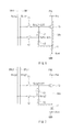
- FIG. 2 is a circuit diagram of a pixel of FIG. 1 .
- FIG. 3 is a waveform diagram illustrating an exemplary operation of the display device of FIG. 1 .
- FIG. 4 is a circuit diagram illustrating an exemplary operation of the display device of FIG. 1 .
- FIG. 5 is a circuit diagram illustrating an exemplary operation following FIG. 4 .
- FIG. 6 is a circuit diagram illustrating an exemplary operation following FIG. 5 .
- FIG. 7 is a circuit diagram illustrating an exemplary operation following FIG. 6 .
- FIG. 8 is a circuit diagram of a modification of the pixel of FIG. 2 .
- FIG. 9 is a waveform diagram illustrating an exemplary operation of a display device including the pixel of FIG. 8 .
- FIG. 10 is a plan view illustrating a schematic configuration of a module including the above-described display device.
- FIG. 11 is a perspective view illustrating an external appearance of a first application example of the above-described display device.
- FIG. 12A is a perspective view illustrating an external appearance of a second application example as seen from a front side
- FIG. 12B is a perspective view illustrating an external appearance as seen from a back side.
- FIG. 13 is a perspective view illustrating an external appearance of a third application example.
- FIG. 14 is a perspective view illustrating an external appearance of a fourth application example.
- FIGS. 15A to 15G illustrate fifth application example
- FIG. 15A is a front elevational view in an opened state
- FIG. 15B is a side view in an opened state
- FIG. 15C is a front elevational view in a closed state
- FIG. 15D is a left side view
- FIG. 15E is a right side view
- FIG. 15F is a top view
- FIG. 15G is a bottom view.
- FIG. 16 is a diagram illustrating an exemplary structure of a pixel of the related art.
- FIG. 17 is a waveform diagram illustrating an exemplary operation of a display device including a pixel of the related art.
- FIG. 1 illustrates an example of general configuration of a display device 1 according to an embodiment of the present disclosure.
- the display device 1 includes a display panel 10 , and a drive circuit 20 configured around the display panel 10 .
- the display panel 10 includes a plurality of display pixels 14 two-dimensionally disposed all over a display region 10 A of the display panel 10 .
- the display panel 10 drives each of the display pixels 14 in an active-matrix manner to display an image based on an externally inputted video signal 20 A.
- Each display pixel 14 includes a pixel 13 R for red, a pixel 13 G for green, and a pixel 13 B for blue, for example.
- pixel 13 is used as a collective term for the pixels 13 R, 13 G, and 13 B.
- the pixel 13 R has, for example, an organic EL element 11 R, and a pixel circuit 12 .
- the pixel 13 G has, for example, an organic EL element 11 G, and the pixel circuit 12 .
- the pixel 13 B has, for example, an organic EL element 11 B, and the pixel circuit 12 .
- the organic EL element 11 R is an organic EL element which emits red light
- the organic EL element 11 G is an organic EL element which emits green light
- the organic EL element 11 B is an organic EL element which emits blue light.
- organic EL element 11 is used as a collective term for the organic EL elements 11 R, 11 G, and 11 B. It is to be noted that, each of the organic EL elements 11 R, 11 G, and 11 B corresponds to a specific example of “light-emitting element” of the embodiment of the present disclosure.
- the organic EL element 11 has a configuration in which, for example, an anode, an organic layer and a cathode are laminated in order.
- the organic layer has, for example, a laminated structure in which, a hole injection layer for enhancing hole injection efficiency, a hole transport layer for enhancing hole transport efficiency to a light emitting layer, the light emitting layer for generating light through electron-hole recombination, and an electron transport layer for enhancing electron transport efficiency to the light emitting layer are laminated in the order starting from the anode side.
- the pixel circuit 12 has, for example, transistors T 1 , T 2 , and T 3 , and holding capacitors C 1 and C 2 .
- the transistors T 1 and T 2 correspond to specific examples of “a sampling circuit” of the present disclosure
- the transistor T 3 corresponds to a specific example of “a drive circuit” of the present disclosure
- the holding capacitors C 1 and C 2 correspond to specific examples of “a holding circuit” of the present disclosure.
- the transistor T 1 samples a voltage of the signal line DTL 1 and writes the voltage in a gate of the transistor T 3 .
- the transistor T 2 samples a voltage of the signal line DTL 2 and writes the voltage in a connection point A between the holding capacitor C 1 and the holding capacitor C 2 .
- the transistor T 3 drives the organic EL element 11 (the transistor T 3 controls the current flowing through the organic EL element 11 ).
- the holding capacitors C 1 and C 2 hold the voltage sampled by the transistors T 1 and T 2 , and holds a predetermined voltage between the gate and a source of the transistor T 3 .
- Each of the transistors T 1 , T 2 , and T 3 is configured of a thin-film transistor (TFT) of an n channel MOS type, for example. It is to be noted that, each of the transistors T 1 , T 2 , and T 3 may be configured of a TFT of a p channel MOS type.
- the display panel 10 has pairs of write lines WSL 1 and WSL 2 extending in the row direction, pairs of signal lines DTL 1 and DTL 2 extending in the column direction, a plurality of power source lines PSL extending in the row direction, and a power source line GND.
- the pixel 13 is provided in the proximity of the intersection of each signal line DTL 1 and each write line WSL 1 .
- Each signal line DTL 1 is connected to an output terminal (not shown) of a signal line drive circuit 23 described later and a source or a drain of the transistor T 1 .
- Each signal line DTL 2 is connected to an output terminal (not shown) of the signal line drive circuit 23 described later and a source or a drain of the transistor T 2 .
- Each write line WSL 1 is connected to an output terminal (not shown) of a write line drive circuit 24 described later and a gate of the transistor T 1 .
- Each write line WSL 2 is connected to an output terminal (not shown) of the write line drive circuit 24 described later and a gate of the transistor T 2 .
- Each power source line PSL is connected to an output terminal (not shown) of a power source which outputs a fixed voltage Vcc and the source or the drain of the transistor T 3 .
- the power source line GND is connected to a wiring (not shown) which is set to a voltage Vcat (for example, ground potential) corresponding to a reference potential and the cathode of the organic EL element 11 .
- the gate of the transistor T 1 is connected to the write line WSL 1 .
- the source or the drain of the transistor T 1 is connected to the signal line DTL 1 , and one of the source and the drain of the transistor T 1 which is not connected to the signal line DTL 1 is connected to the gate of the transistor T 3 .
- the gate of the transistor T 2 is connected to the write line WSL 2 .
- the source or the drain of the transistor T 2 is connected to the signal line DTL 2 , and one of the source and the drain of the transistor T 2 which is not connected to the signal line DTL 2 is connected to the connection point A.
- the source or the drain of the transistor T 3 is connected to the power source line PSL, and one of the source and the drain of the transistor T 3 which is not connected to the power source line PSL is connected to the anode of the organic EL element 11 .
- One end of the holding capacitor C 1 is connected to the gate of the transistor T 3 , and the other end of the holding capacitor C 1 is connected to one end of the holding capacitor C 2 .
- the other end of the holding capacitor C 2 is connected to one of the source and the drain of the transistor T 3 which is not connected to the power source line PSL.
- the holding capacitors C 1 and C 2 are serially inserted between the gate and the source of the transistor T 3 .
- the anode of the organic EL element 11 is connected to one of the source and the drain of the transistor T 3 which is not connected to the power source line PSL, and the cathode of the organic EL element 11 is connected to the power source line GND.
- the drive circuit 20 has, for example, a timing generation circuit 21 , a video signal processing circuit 22 , the signal line drive circuit 23 , the write line drive circuit 24 , and the power source line drive circuit 25 .
- the timing generation circuit 21 controls the video signal processing circuit 22 , the signal line drive circuit 23 , the write line drive circuit 24 , and the power source line drive circuit 25 to operate in conjunction with one another. In response to (or, in synchronization with) an externally-inputted synchronizing signal 20 B, for example, the timing generation circuit 21 outputs a control signal 21 A to the above-described circuits.
- the video signal processing circuit 22 carries out a predetermined correction of an externally-inputted digital video signal 20 A, and converts the corrected video signal into an analog signal and outputs the signal to the signal line drive circuit 23 .
- the predetermined correction includes a gamma correction, an overdrive correction, and the like. Further, the video signal processing circuit 22 generates, from the video signal 20 A, a video signal 22 A to be outputted to the signal line DTL 1 , and a video signal 22 B to be outputted to the signal line DTL 2 .
- the signal line drive circuit 23 In response to (or, in synchronization with) an input of the control signal 21 A, the signal line drive circuit 23 outputs the video signal 22 A inputted from the video signal processing circuit 22 to each signal line DTL 1 . Meanwhile, in response to (or, in synchronization with) an input of the control signal 21 A, the signal line drive circuit 23 outputs the video signal 22 B, which is an analog signal, inputted from the video signal processing circuit 22 to each signal line DTL 2 .
- the signal line drive circuit 23 may, for example, output three kinds of voltages (Vofs, Vsig 1 , and Vsig 2 ) according to an input of the control signal 21 A.
- the signal line drive circuit 23 regularly supplies a pixel 13 selected by the write line drive circuit 24 with two kinds of voltages (Vofs and Vsig 1 ). Further, through the signal line DTL 2 , the signal line drive circuit 23 regularly supplies a pixel 13 selected by the write line drive circuit 24 with two kinds of voltages (Vofs and Vsig 2 ).
- the voltage Vofs is a basic voltage, and is set to a voltage value lower than the threshold voltage of the organic EL element 11 .
- the voltage Vofs is set to a value such that Vofs ⁇ Vss is higher than a threshold voltage Vth of the transistor T 3 .
- each of the voltages Vsig 1 and Vsig 2 is set to a voltage value commensurate with a gray-scale.
- the maximum value of each of the voltages Vsig 1 and Vsig 2 is set to a value lower than the maximum value of a voltage outputted to the signal line DTL provided corresponding to the pixel circuit 100 of known type shown in FIG. 16 .
- the write line drive circuit 24 In response to (or, in synchronization with) an input of the control signal 21 A, the write line drive circuit 24 sequentially selects a plurality of the write lines WSL 1 on a predetermined unit basis (for example, one at a time), and sequentially selects a plurality of the write lines WSL 2 on a predetermined unit basis (for example, one at a time).
- the write line drive circuit 24 may output two kinds of voltages (Von and Voff) in response to an input of the control signal 21 A, for example.
- the write line drive circuit 24 supplies a pixel 13 to be driven with two kinds of voltages (Von and Voff), and, through the write line WSL 2 , supplies a pixel 13 to be driven with two kinds of voltages (Von and Voff).
- the voltage Von is set to a value higher than the on voltage of the transistors Tr 1 and T 2 .
- the voltage Voff is set to a value lower than the on voltage of the transistors Tr 1 and T 2 .
- the power source line drive circuit 25 is capable of outputting two kinds of voltages (Vcc and Vss) in response to (or, in synchronization with) an input of the control signal 21 A. Specifically, through the power source line PSL, the power source line drive circuit 25 supplies a pixel 13 to be driven with two kinds of voltages (Vcc and Vss).
- the voltage Vss is set to a voltage value lower than a voltage which is the sum of the threshold voltage of the organic EL element 11 and the cathode voltage of the organic EL element 11 .
- the voltage Vss is set to such a value that Vofs ⁇ Vss is larger than the threshold voltage Vth of the transistor T 3 .
- the voltage Vcc is set to a voltage value higher than a voltage which is the sum of the threshold voltage of the organic EL element 11 and the cathode voltage of the organic EL element 11 .
- the present embodiment incorporates a compensation operation for a variation in I-V characteristics of the organic EL element 11 and a correction operation for a variation in the threshold voltage and the mobility of the transistor T 3 so that, even in the case where I-V characteristics of the organic EL element 11 is changed over time, or where the threshold voltage and the mobility of the transistor T 3 are changed over time, the light-emission luminance of the organic EL element 11 may be kept constant without being affected by the changes over time.
- FIG. 3 illustrates exemplary waveforms of voltages applied to one of the pixels 13 of the display device 1 .
- FIG. 3 shows a state where two kinds of voltages (Vcc and Vss) are applied to the power source line PSL, and three kinds of voltages (Vofs, Vsig 1 , and Vsig 2 ) are applied to the signal lines DTL 1 and DTL 2 , and two kinds of voltages (Von and Voff) are applied to the write lines WSL 1 and WSL 2 .
- FIG. 3 shows temporal changes of the gate voltage Vg and the source voltage Vs of the transistor T 3 , and the voltage of the connection point A in response to applications of voltage to the power source line PSL, the signal lines DTL, and the write lines WSL.
- the transistors T 1 and T 2 are in an off state, and the transistor T 3 operates in a saturation region. Therefore, a current corresponding to the voltage between the gate and the the source of the transistor T 3 flows through the organic EL element 11 , and the organic EL element 11 emits light with luminance corresponding to the current value.
- the power source line drive circuit 25 decreases the voltage of the power source line PSL from Vcc to Vss (t 1 ). Then, the source voltage Vs becomes Vss, and the light emission of the organic EL element 11 is stopped. Next, the signal line drive circuit 23 switches the voltage of the signal line DTL 1 from Vsig 1 to Vofs, and switches the voltage of the signal line DTL 2 from Vsig 2 to Vofs. Thereafter, while the voltage of the power source line PSL is Vss, the write line drive circuit 24 raises the voltages of the write lines WSL 1 and WSL 2 from Voff to Von (t 2 ).
- the signal line DTL 1 is connected to the gate of the transistor T 3 , and the signal line DTL 2 is connected to the connection point A.
- the gate voltage Vg of the transistor T 3 becomes Vofs
- the voltage of the connection point A also becomes Vofs.
- the voltage between the gate and the source of the transistor T 3 (Vofs ⁇ Vss) is higher than the threshold voltage Vth of the transistor T 3 .
- a threshold correction is carried out. Specifically, while the voltages of the signal lines DTL 1 and DTL 2 are Vofs, the power source line drive circuit 25 raises the voltage of the power source line PSL from Vss to Vcc (t 3 ). Then, as shown in FIG. 4 , the current Ids flows between the drain and the source of the transistor T 3 to raise the source voltage Vs of the transistor T 3 . After the lapse of a certain period of time, the voltage between the gate and the source of the transistor T 3 becomes Vth.
- Ve 1 Vofs ⁇ Vth ⁇ Vcat+Vthe 1
- Vcat represents the cathode voltage of the organic EL element 11
- Vthe 1 represents the threshold voltage of the organic EL element 11 . Therefore, the organic EL element 11 is in a cut-off state.
- the write line drive circuit 24 decreases the voltages of the write lines WSL 1 and WSL 2 from Von to Voff (t 4 ). Then, the gate of the transistor T 3 is set to a floating state, and the threshold correction is temporarily stopped.
- a sampling of the voltages of the signal lines DTL 1 and DTL 2 is carried out at another row (pixel 13 ) different from the row (pixel 13 ) which has undergone the threshold correction.
- a first writing•mobility correction is carried out. Specifically, after the signal line drive circuit 23 switches the voltage of the signal line DTL 1 from Vofs to Vsig 1 , the write line drive circuit 24 raises the voltage of the write lines WSL 1 and WSL 2 from Voff to Von (t 5 ) to connect the gate of the transistor T 3 to the signal line DTL 1 . At this time, at least until the voltages of the write lines WSL 1 and WSL 2 are decreased from Von to Voff by the write line drive circuit 24 , the signal line drive circuit 23 maintains the voltage of the signal line DTL 2 at Vofs.
- the first writing•mobility correction corresponds to a specific example of “a first sampling” of the present disclosure.
- the gate voltage of the transistor T 3 becomes Vsig 1 .
- the anode voltage of the organic EL element 11 at this stage is still lower than the threshold voltage of the organic EL element 11 , and the organic EL element 11 is in a cut-off state. Therefore, since the current Ids flows through a capacitor element (not shown) of the organic EL element 11 to charge the capacitor element, the source voltage Vs of the transistor T 3 gradually rises.
- the current of the transistor T 3 is used to charge the parasitic capacitance of the holding capacitor C 2 and the organic EL element 11 .
- the threshold correction of the transistor T 3 is already completed, so that the current flowing through the transistor T 3 corresponds to the mobility ⁇ of the transistor T 3 .
- the write line drive circuit 24 decreases the voltages of the write lines WSL 1 and WSL 2 from Von to Voff (t 6 ) to turn off the transistors T 1 and T 2 .
- the signal line drive circuit 23 switches the voltage of the signal line DTL 2 from Vofs to Vsig 2 . At this time, the signal line drive circuit 23 maintains the voltage of the signal line DTL 1 at Vsig 1 .
- the source voltage Vs of the transistor T 3 continues to rise. Along with the rising of the source voltage Vs, the voltage of the connection point A between the holding capacitors C 1 and C 2 and the gate voltage Vg of the transistor T 3 are also raised. The increment at this time is represented by ⁇ V 1 (see FIG. 6 ). At this time, if the source voltage Vs of the transistor T 3 does not exceed the sum of the threshold voltage of the organic EL element 11 and the cathode voltage of the organic EL element 11 , then the organic EL element 11 does not emit light.
- a second writing•mobility correction is carried out. Specifically, the write line drive circuit 24 raises the voltage of the write line WSL 2 from Voff to Von (t 7 ), and connects the connection point A between the holding capacitors C 1 and C 2 to the signal line DTL 2 . At this time, at least until the voltage of the write line WSL 2 is decreased from Von to Voff, the write line drive circuit 24 maintains the voltage of the write line WSL 1 at Voff.
- the second writing•mobility correction corresponds to a specific example of “a second sampling” of the present disclosure.
- the variation in voltage at the connection point A is inputted to the gate of the transistor T 3 through the holding capacitor C 1 . Therefore, as shown in FIG. 7 , the gate voltage Vg of the transistor T 3 is raised by ⁇ V in accordance to the amount of variation in voltage at the connection point A, and becomes Vsig 1 + ⁇ V. As a result, again, the mobility correction of the transistor T 3 is started to raise the source voltage Vs of the transistor T 3 .
- the write line drive circuit 24 decreases the voltage of the write line WSL 2 from Von to Voff (t 8 ). Then, the gate of the transistor T 3 is set to a floating state, and the current Ids flows between the drain and the source of the transistor T 3 to raise the source voltage Vs. As a result, the organic EL element 11 emits light with a desired luminance. It is to be noted that, in the light emission period, the signal amplitude inputted to the pixel 13 is Vsig 1 + ⁇ V ⁇ Vofs, which is larger than Vsig 1 ⁇ Vofs.
- the voltage of the signal line DTL 1 is sampled by the transistor T 2 , and written in the gate of the transistor T 3 . Further, the voltage of the signal line DTL 2 is sampled by the transistor T 2 , and written in the holding capacitor C 1 .
- the gate voltage Vg of the transistor T 1 may be raised to a voltage higher than the voltage of the signal line DTL 1 to turn on the transistor T 1 .
- the voltage inputted between the gate and the source of the transistor T 1 may be set to a voltage higher than Vsig 1 ⁇ Vofs (i.e., Vsig 1 + ⁇ V ⁇ Vofs).
- Vsig 1 is the maximum output voltage of the signal line drive circuit 23
- a voltage higher than the maximum output voltage of the signal line drive circuit 23 is inputted to the pixel 13 .
- the amplitude of the signal line drive circuit 23 may be spuriously made large by the pixel circuit 12 .
- an effect similar to increasing the output of the signal line drive circuit 23 which applies the voltage to the signal lines DTL 1 and DTL 2 may be obtained. Consequently, high-luminance may be obtained while suppressing the power consumption of the signal line drive circuit 23 .
- the second writing•mobility correction is carried out before 1H elapses from the start of the first writing•mobility correction
- the second writing•mobility correction may be carried out after 1H has elapsed from the start of the first writing•mobility correction. Even in this case, similarly to the above-described embodiment, it is possible to obtain the effect similar to increasing the output of the signal line drive circuit 23 which applies the voltage to the signal lines DTL 1 and DTL 2 .
- the gate of the transistor T 3 may be connected to the connection point A between the holding capacitors C 1 and C 2 , and the gate of the transistor T 1 may be connected to the write line WSL 2 , and the gate of the transistor T 2 may be connected to the write line WSL 1 .
- the signal line DTL 2 may be connected to one of the source and the drain of the transistor T 1 which is not connected to the holding capacitor C 1 , and the signal line DTL 1 may be connected to one of the source and drain of the transistor T 2 which is not connected to the gate of the transistor T 3 .
- FIG. 9 illustrates exemplary voltage waveforms applied to a pixel 13 of the display device 1 according to the present modification.
- FIG. 9 shows a state where two kinds of voltages (Vcc and Vss) are applied to a power source line PSL, three kinds of voltages (Vofs, Vsig 1 , and Vsig 2 ) are applied to signal lines DTL 1 and DTL 2 , and two kinds of voltages (Von and Voff) are applied to a write line WSL.
- FIG. 9 shows temporal changes of a gate voltage Vg and a source voltage Vs of the transistor T 3 , and a voltage of a connection point B in response to voltages applied to the power source line PSL, the signal line DTL, and the write line WSL.
- transistors T 1 and T 2 are in an off state, and a transistor T 3 operates in a saturation region. Therefore, a current corresponding to the voltage between the gate and the source of the transistor T 3 flows through an organic EL element 11 , and the organic EL element 11 emits light with luminance corresponding to the current value.
- a power source line drive circuit 25 decreases the voltage of the power source line PSL from Vcc to Vss (t 1 ). Then, the source voltage Vs becomes Vss, and the organic EL element 11 is turned off.
- a signal line drive circuit 23 switches the voltage of the signal line DTL 1 from Vsig 1 to Vofs, and switches the voltage of the signal line DTL 2 from Vsig 2 to Vofs. Thereafter, while the voltage of the power source line PSL is Vss, a write line drive circuit 24 raises the voltage of the write lines WSL 1 and WSL 2 from Voff to Von (t 2 ).
- the signal line DTL 1 is connected to the gate of the transistor T 3 , and the signal line DTL 2 is connected to the connection point B between the transistor T 1 and a holding capacitor C 1 .
- the gate voltage Vg of the transistor T 3 becomes Vofs
- the voltage of the connection point B also becomes Vofs.
- the voltage between the gate and the source of the transistor T 3 (Vofs ⁇ Vss) is larger than the threshold voltage Vth of the transistor T 3 .
- the write line drive circuit 24 decreases the voltages of the write lines WSL 1 and WSL 2 from Von to Voff (t 4 ). Then, the gate of the transistor T 3 is set to a floating state, and the threshold correction is temporarily stopped.
- a sampling of the voltages of the signal lines DTL 1 and DTL 2 is carried out at another row (pixel 13 ) different from the row (pixel 13 ) which has undergone the threshold correction.
- a first writing•mobility correction is carried out. Specifically, after the signal line drive circuit 23 switches the voltage of the signal line DTL 1 from Vofs to Vsig 1 , the write line drive circuit 24 raises the voltages of the write lines WSL 1 and WSL 2 from Voff to Von (t 5 ) to connect the gate of the transistor T 3 to the signal line DTL 1 . At this time, at least until the voltages of the write lines WSL 1 and WSL 2 are decreased from Von to Voff by the write line drive circuit 24 , the signal line drive circuit 23 maintains the voltage of the signal line DTL 2 at Vofs. It is to be noted that, the first writing•mobility correction corresponds to a specific example of “a first sampling” of the present disclosure.
- the gate voltage Vg of the transistor T 3 becomes Vsig 1 .
- the anode voltage of the organic EL element 11 at this stage is still lower than the threshold voltage of the organic EL element 11 , and the organic EL element 11 is in a cut-off state. Therefore, since the current Ids flows through a capacitor element (not shown) of the organic EL element 11 to charge the capacitor element, the source voltage Vs of the transistor T 3 gradually rises.
- the current of the transistor T 3 is used to charge the parasitic capacitance of the holding capacitor C 2 and the organic EL element 11 .
- the threshold correction of the transistor T 3 is already completed, so that the current flowing through the transistor T 3 corresponds to the mobility ⁇ of the transistor T 3 .
- the write line drive circuit 24 decreases the voltage of the write lines WSL 1 and WSL 2 from Von to Voff (t 6 ) to turn off the transistors T 1 and T 2 .
- the signal line drive circuit 23 switches the voltage of the signal line DTL 2 from Vofs to Vsig 2 . At this time, the signal line drive circuit 23 maintains the voltage of the signal line DTL 1 at Vsig 1 .
- the source voltage Vs of the transistor T 3 continues to rise. Along with the rising of the source voltage Vs, the voltages of the connection points A and B are also raised. The increment at this time is represented by ⁇ V 1 . At this time, if the source voltage Vs of the transistor T 3 does not exceed the sum of the threshold voltage of the organic EL element 11 and the cathode voltage of the organic EL element 11 , then the organic EL element 11 does not emit light.
- a second writing•mobility correction is carried out. Specifically, the write line drive circuit 24 raises the voltage of the write line WSL 2 from Voff to Von (t 7 ), and connects the connection point B to the signal line DTL 2 . At this time, at least until the voltage of the write line WSL 2 is decreased from Von to Voff, the write line drive circuit 24 maintains the voltage of the write line WSL 1 at Voff.
- the second writing•mobility correction corresponds to a specific example of “a second sampling” of the present disclosure.
- the variation in voltage at the connection point B is inputted to the gate of the transistor T 3 through the holding capacitor C 1 . Therefore, the gate voltage of the transistor T 3 is raised by ⁇ V in accordance to the amount of variation in voltage at the connection point B, and becomes Vsig 1 + ⁇ V. As a result, again, the mobility correction of the transistor T 3 is started to raise the source voltage Vs of the transistor T 3 .
- the write line drive circuit 24 decreases the voltage of the write line WSL 2 from Von to Voff (t 8 ). Then, the gate of the transistor T 3 is set to a floating state, and the current Ids flows between the drain and the source of the transistor T 3 to raise the source voltage Vs. As a result, the organic EL element 11 emits light with a desired luminance. It is to be noted that, in the light emission period, the signal amplitude inputted to the pixel 13 is Vsig 1 + ⁇ V ⁇ Vofs, which is larger than Vsig 1 ⁇ Vofs.
- the display device 1 of the present modification operates in substantially the same manner as in the above-described embodiment. Accordingly, as is the case with the above-described embodiment, an effect similar to increasing the output of the signal line drive circuit 23 which applies the voltage to the signal lines DTL 1 and DTL 2 may be obtained also in the present modification. Consequently, high-luminance may be obtained while suppressing the power consumption of the signal line drive circuit 23 .
- the display device 1 of the above-described embodiment and so forth may be applied to display devices of electronic unit in various fields for displaying an externally inputted video signal or an internally generated video signal as an image or a video.
- Typical examples of such electronic unit include a television device, a digital camera, a notebook personal computer, a mobile terminal device such as a mobile phone, and a video camera.
- the display device 1 of the above-described embodiment and so forth is incorporated in various kinds of electronic unit of a first to fifth application examples described below and the like, as a module shown in FIG. 10 , for example.
- the module shown in FIG. 10 has, for example, a region 210 which is provided on one side of a substrate 2 and exposed from a member (not shown) enclosing a display section 30 .
- Wirings of a timing generation circuit 21 , a video signal processing circuit 22 , a signal line drive circuit 23 , a write line drive circuit 24 , and a power source line drive circuit 25 are extended to the exposed region 210 to configure an external connection terminal (not shown).
- the external connection terminal may be provided with a flexible printed circuit (FPC) 220 for inputting and outputting signals.
- FPC flexible printed circuit
- FIG. 11 illustrates an external appearance of a television device to which the display device 1 of the above-described embodiment and so forth is applied.
- This television device has, for example, a video display screen section 300 including a front panel 310 and a filter glass 320 , and the video display screen section 300 is configured of the display device 1 of the above-described embodiment and so forth.
- FIGS. 12A and 12B illustrate external appearances of a digital camera to which the display device 1 of the above-described embodiment and so forth is applied.
- This digital camera has, for example, a light emitting section 410 for generating flash light, a display section 420 , a menu switch 430 , and a shutter button 440 , and the display section 420 is configured of the display device 1 of the above-described embodiment and so forth.
- FIG. 13 illustrates an external appearance of a notebook personal computer to which the display device 1 of the above-described embodiment and so forth is applied.
- This notebook personal computer has, for example, a main body 510 , a keyboard 520 for input operation of letters and the like, and a display section 530 for displaying images, and the display section 530 is configured of the display device 1 of the above-described embodiment and so forth.
- FIG. 14 illustrates an external appearance of a video camera to which the display device 1 of the above-described embodiment and so forth is applied.
- This video camera has, for example, a main body section 610 , a lens 620 which is adapted to take an image of a subject and provided on the front side of the main body section 610 , a start/stop switch 630 used when capturing an image, and a display section 640 , and the display section 640 is configured of the display device 1 of the above-described embodiment and so forth.
- FIGS. 15A to 15G illustrate external appearances of a mobile phone to which the display device 1 of the above-described embodiment and so forth is applied.
- This mobile phone has, for example, an upper housing 710 , a lower housing 720 , a connecting section (or a hinge section) 730 which connects the upper housing 710 and the lower housing 720 , a display 740 , a sub-display 750 , a picture light 760 , and a camera 770 .
- the display 740 or the sub-display 750 is configured of the display device 1 of the above-described embodiment and so forth.
- the configuration of the pixel circuit 12 for active matrix drive is not limited to the configuration described in the above-described embodiment and so forth, and a capacitative element and a transistor may be included in the pixel circuit 12 if necessary.
- a capacitative element and a transistor may be included in the pixel circuit 12 if necessary.
- three or more capacitative elements may be provided between the gate and the source of the transistor T 3 .
- two or more capacitative elements may be provided between the gate of the transistor T 3 and the source of the transistor T 1
- two or more capacitative elements may be provided between the gate and the source of the transistor T 3 , for example.
Landscapes
- Engineering & Computer Science (AREA)
- Physics & Mathematics (AREA)
- General Physics & Mathematics (AREA)
- Theoretical Computer Science (AREA)
- Computer Hardware Design (AREA)
- Control Of El Displays (AREA)
- Microelectronics & Electronic Packaging (AREA)
- Optics & Photonics (AREA)
- Electroluminescent Light Sources (AREA)
- Control Of Indicators Other Than Cathode Ray Tubes (AREA)
Applications Claiming Priority (2)
| Application Number | Priority Date | Filing Date | Title |
|---|---|---|---|
| JP2011-048377 | 2011-03-04 | ||
| JP2011048377A JP5804732B2 (ja) | 2011-03-04 | 2011-03-04 | 駆動方法、表示装置および電子機器 |
Publications (2)
| Publication Number | Publication Date |
|---|---|
| US20120223978A1 US20120223978A1 (en) | 2012-09-06 |
| US8976090B2 true US8976090B2 (en) | 2015-03-10 |
Family
ID=46730600
Family Applications (1)
| Application Number | Title | Priority Date | Filing Date |
|---|---|---|---|
| US13/406,066 Expired - Fee Related US8976090B2 (en) | 2011-03-04 | 2012-02-27 | Pixel circuit with multiple holding capacitors, method of driving the pixel circuit, display panel, display device and electronic unit |
Country Status (3)
| Country | Link |
|---|---|
| US (1) | US8976090B2 (enExample) |
| JP (1) | JP5804732B2 (enExample) |
| CN (1) | CN102654979B (enExample) |
Cited By (22)
| Publication number | Priority date | Publication date | Assignee | Title |
|---|---|---|---|---|
| US11100855B2 (en) | 2017-12-22 | 2021-08-24 | Semiconductor Energy Laboratory Co., Ltd. | Display device and electronic device |
| US11183137B2 (en) | 2018-02-23 | 2021-11-23 | Semiconductor Energy Laboratory Co., Ltd. | Operation method of display apparatus |
| US11204533B2 (en) | 2018-03-06 | 2021-12-21 | Semiconductor Energy Laboratory Co., Ltd. | Display device and electronic device |
| US11302278B2 (en) | 2017-09-15 | 2022-04-12 | Semiconductor Energy Laboratory Co., Ltd. | Display device including pixel and electronic device |
| US11355577B2 (en) | 2019-08-29 | 2022-06-07 | Semiconductor Energy Laboratory Co., Ltd. | Display device |
| US11355082B2 (en) | 2018-02-01 | 2022-06-07 | Semiconductor Energy Laboratory Co., Ltd. | Display device and electronic device |
| US11373610B2 (en) | 2018-12-26 | 2022-06-28 | Semiconductor Energy Laboratory Co., Ltd. | Display apparatus including circuit and pixel |
| US11423844B2 (en) | 2018-05-17 | 2022-08-23 | Semiconductor Energy Laboratory Co., Ltd. | Display device and electronic device |
| US11435637B2 (en) | 2018-09-21 | 2022-09-06 | Semiconductor Energy Laboratory Co., Ltd. | Display apparatus and electronic device |
| US11450694B2 (en) | 2018-08-21 | 2022-09-20 | Semiconductor Energy Laboratory Co., Ltd. | Display apparatus and electronic device |
| US11455940B2 (en) | 2018-06-06 | 2022-09-27 | Semiconductor Energy Laboratory Co., Ltd. | Method for actuating display device |
| US11475834B2 (en) | 2016-04-15 | 2022-10-18 | Samsung Display Co., Ltd. | Pixel circuit and method of driving the same |
| US11513405B2 (en) | 2018-04-26 | 2022-11-29 | Semiconductor Energy Laboratory Co., Ltd. | Display device and electronic device |
| US11557235B1 (en) * | 2021-12-15 | 2023-01-17 | Raytheon Company | Switch-based grid for resiliency and yield improvement |
| US11574573B2 (en) | 2017-09-05 | 2023-02-07 | Semiconductor Energy Laboratory Co., Ltd. | Display system |
| US11615756B2 (en) | 2017-12-22 | 2023-03-28 | Semiconductor Energy Laboratory Co., Ltd. | Display device, semiconductor device, and electronic device |
| US11645992B2 (en) | 2018-03-29 | 2023-05-09 | Semiconductor Energy Laboratory Co., Ltd. | Method for operating display device with potentials higher and lower than maximum and minimum potentials generated by source driver circuit |
| US11663990B2 (en) | 2018-11-09 | 2023-05-30 | Semiconductor Energy Laboratory Co., Ltd. | Display apparatus and electronic device |
| US11763766B2 (en) | 2017-12-22 | 2023-09-19 | Semiconductor Energy Laboratory Co., Ltd. | Display panel, display device, input/output device, and data processing device |
| US11793010B2 (en) | 2018-06-06 | 2023-10-17 | Semiconductor Energy Laboratory Co., Ltd. | Display device, display module, and electronic device |
| US11990502B2 (en) * | 2017-08-31 | 2024-05-21 | Semiconductor Energy Laboratory Co., Ltd. | Display device and electronic device |
| US12165575B2 (en) | 2018-09-12 | 2024-12-10 | Semiconductor Energy Laboratory Co., Ltd. | Display device |
Families Citing this family (16)
| Publication number | Priority date | Publication date | Assignee | Title |
|---|---|---|---|---|
| JP5305105B2 (ja) * | 2009-11-11 | 2013-10-02 | ソニー株式会社 | 表示装置およびその駆動方法ならびに電子機器 |
| JP2016528664A (ja) * | 2013-06-07 | 2016-09-15 | コモンウェルス サイエンティフィック アンド インダストリアル リサーチ オーガナイゼーション | エレクトロルミネセントデバイス |
| JP2015014764A (ja) * | 2013-07-08 | 2015-01-22 | ソニー株式会社 | 表示装置、表示装置の駆動方法、及び、電子機器 |
| TWI594221B (zh) * | 2013-11-12 | 2017-08-01 | 友達光電股份有限公司 | 像素結構及其驅動方法 |
| TWI498873B (zh) * | 2013-12-04 | 2015-09-01 | Au Optronics Corp | 有機發光二極體電路及其驅動方法 |
| WO2019092540A1 (en) * | 2017-11-09 | 2019-05-16 | Semiconductor Energy Laboratory Co., Ltd. | Semiconductor device, display device, and electronic device |
| CN115359757B (zh) | 2017-11-09 | 2025-05-27 | 株式会社半导体能源研究所 | 显示装置及其工作方法以及电子设备 |
| KR20250162955A (ko) * | 2017-12-06 | 2025-11-19 | 가부시키가이샤 한도오따이 에네루기 켄큐쇼 | 반도체 장치, 표시 장치, 전자 기기, 및 동작 방법 |
| WO2019155320A1 (ja) * | 2018-02-09 | 2019-08-15 | 株式会社半導体エネルギー研究所 | 表示装置の駆動方法 |
| JP7176864B2 (ja) * | 2018-06-06 | 2022-11-22 | 株式会社半導体エネルギー研究所 | 表示装置および電子機器 |
| JP7487111B2 (ja) | 2018-12-19 | 2024-05-20 | 株式会社半導体エネルギー研究所 | 表示装置および電子機器 |
| WO2020148604A1 (ja) * | 2019-01-18 | 2020-07-23 | 株式会社半導体エネルギー研究所 | 表示装置および電子機器 |
| WO2020229911A1 (ja) * | 2019-05-10 | 2020-11-19 | 株式会社半導体エネルギー研究所 | 表示装置および電子機器 |
| CN110491338B (zh) * | 2019-08-28 | 2021-02-02 | 京东方科技集团股份有限公司 | 像素电路及其驱动方法、发光控制电路及方法、显示装置 |
| CN111710291B (zh) * | 2020-07-06 | 2023-11-10 | 天津中科新显科技有限公司 | 一种适用于多电源的电流型像素驱动电路及方法 |
| US20230255060A1 (en) * | 2020-07-09 | 2023-08-10 | Semiconductor Energy Laboratory Co., Ltd. | Display apparatus and electronic device |
Citations (5)
| Publication number | Priority date | Publication date | Assignee | Title |
|---|---|---|---|---|
| US20060022907A1 (en) * | 2004-07-05 | 2006-02-02 | Sony Corporation | Pixel circuit, display device, driving method of pixel circuit, and driving method of display device |
| US20090256827A1 (en) * | 2008-04-15 | 2009-10-15 | Sony Corporation | Display device and output buffer circuit for driving the same |
| JP2009300697A (ja) | 2008-06-12 | 2009-12-24 | Sony Corp | 表示装置およびその駆動方法ならびに電子機器 |
| US8253659B2 (en) * | 2008-11-28 | 2012-08-28 | Global Oled Technology, Llc. | Display device and pixel circuit |
| US8305303B2 (en) * | 2008-02-22 | 2012-11-06 | Lg Display Co., Ltd. | Organic light emitting diode display and method of driving the same |
Family Cites Families (7)
| Publication number | Priority date | Publication date | Assignee | Title |
|---|---|---|---|---|
| JP2003216109A (ja) * | 2002-01-28 | 2003-07-30 | Sanyo Electric Co Ltd | 表示装置およびその表示の制御方法 |
| JP4831392B2 (ja) * | 2004-07-05 | 2011-12-07 | ソニー株式会社 | 画素回路及び表示装置 |
| WO2007018006A1 (ja) * | 2005-08-05 | 2007-02-15 | Sharp Kabushiki Kaisha | 表示装置 |
| JP2008249743A (ja) * | 2007-03-29 | 2008-10-16 | Sony Corp | 表示装置、表示装置の駆動方法および電子機器 |
| JP2010266492A (ja) * | 2009-05-12 | 2010-11-25 | Sony Corp | 画素回路、表示装置、画素回路の駆動方法 |
| JP5310244B2 (ja) * | 2009-05-12 | 2013-10-09 | ソニー株式会社 | 表示装置、表示方法 |
| JP2010286541A (ja) * | 2009-06-09 | 2010-12-24 | Seiko Epson Corp | 発光装置、電子機器、および発光装置の駆動方法 |
-
2011
- 2011-03-04 JP JP2011048377A patent/JP5804732B2/ja not_active Expired - Fee Related
-
2012
- 2012-02-27 US US13/406,066 patent/US8976090B2/en not_active Expired - Fee Related
- 2012-03-05 CN CN201210055066.1A patent/CN102654979B/zh active Active
Patent Citations (5)
| Publication number | Priority date | Publication date | Assignee | Title |
|---|---|---|---|---|
| US20060022907A1 (en) * | 2004-07-05 | 2006-02-02 | Sony Corporation | Pixel circuit, display device, driving method of pixel circuit, and driving method of display device |
| US8305303B2 (en) * | 2008-02-22 | 2012-11-06 | Lg Display Co., Ltd. | Organic light emitting diode display and method of driving the same |
| US20090256827A1 (en) * | 2008-04-15 | 2009-10-15 | Sony Corporation | Display device and output buffer circuit for driving the same |
| JP2009300697A (ja) | 2008-06-12 | 2009-12-24 | Sony Corp | 表示装置およびその駆動方法ならびに電子機器 |
| US8253659B2 (en) * | 2008-11-28 | 2012-08-28 | Global Oled Technology, Llc. | Display device and pixel circuit |
Cited By (37)
| Publication number | Priority date | Publication date | Assignee | Title |
|---|---|---|---|---|
| US11984077B2 (en) | 2016-04-15 | 2024-05-14 | Samsung Display Co., Ltd. | Pixel circuit and method of driving the same |
| US11475834B2 (en) | 2016-04-15 | 2022-10-18 | Samsung Display Co., Ltd. | Pixel circuit and method of driving the same |
| US11990502B2 (en) * | 2017-08-31 | 2024-05-21 | Semiconductor Energy Laboratory Co., Ltd. | Display device and electronic device |
| US11574573B2 (en) | 2017-09-05 | 2023-02-07 | Semiconductor Energy Laboratory Co., Ltd. | Display system |
| US11694648B2 (en) | 2017-09-15 | 2023-07-04 | Semiconductor Energy Laboratory Co., Ltd. | Display device with switches connecting signal lines and gate lines |
| US11302278B2 (en) | 2017-09-15 | 2022-04-12 | Semiconductor Energy Laboratory Co., Ltd. | Display device including pixel and electronic device |
| US11763766B2 (en) | 2017-12-22 | 2023-09-19 | Semiconductor Energy Laboratory Co., Ltd. | Display panel, display device, input/output device, and data processing device |
| US11100855B2 (en) | 2017-12-22 | 2021-08-24 | Semiconductor Energy Laboratory Co., Ltd. | Display device and electronic device |
| US11615756B2 (en) | 2017-12-22 | 2023-03-28 | Semiconductor Energy Laboratory Co., Ltd. | Display device, semiconductor device, and electronic device |
| US11355082B2 (en) | 2018-02-01 | 2022-06-07 | Semiconductor Energy Laboratory Co., Ltd. | Display device and electronic device |
| US11626082B2 (en) | 2018-02-01 | 2023-04-11 | Semiconductor Energy Laboratory Co., Ltd. | Display device and electronic device |
| US12106729B2 (en) | 2018-02-01 | 2024-10-01 | Semiconductor Energy Laboratory Co., Ltd. | Display device and electronic device |
| US11183137B2 (en) | 2018-02-23 | 2021-11-23 | Semiconductor Energy Laboratory Co., Ltd. | Operation method of display apparatus |
| US11822198B2 (en) | 2018-03-06 | 2023-11-21 | Semiconductor Energy Laboratory Co., Ltd. | Display device and electronic device |
| US11204533B2 (en) | 2018-03-06 | 2021-12-21 | Semiconductor Energy Laboratory Co., Ltd. | Display device and electronic device |
| US11645992B2 (en) | 2018-03-29 | 2023-05-09 | Semiconductor Energy Laboratory Co., Ltd. | Method for operating display device with potentials higher and lower than maximum and minimum potentials generated by source driver circuit |
| US12282240B2 (en) | 2018-04-26 | 2025-04-22 | Semiconductor Energy Laboratory Co., Ltd. | Display device and electronic device |
| US11513405B2 (en) | 2018-04-26 | 2022-11-29 | Semiconductor Energy Laboratory Co., Ltd. | Display device and electronic device |
| US11762250B2 (en) | 2018-04-26 | 2023-09-19 | Semiconductor Energy Laboratory Co., Ltd. | Display device and electronic device |
| US11423844B2 (en) | 2018-05-17 | 2022-08-23 | Semiconductor Energy Laboratory Co., Ltd. | Display device and electronic device |
| US11798491B2 (en) | 2018-05-17 | 2023-10-24 | Semiconductor Energy Laboratory Co., Ltd. | Display device and electronic device |
| US12469463B2 (en) | 2018-05-17 | 2025-11-11 | Semiconductor Energy Laboratory Co., Ltd. | Display device and electronic device |
| US11455940B2 (en) | 2018-06-06 | 2022-09-27 | Semiconductor Energy Laboratory Co., Ltd. | Method for actuating display device |
| US12161006B2 (en) | 2018-06-06 | 2024-12-03 | Semiconductor Energy Laboratory Co., Ltd. | Display device, display module, and electronic device |
| US11793010B2 (en) | 2018-06-06 | 2023-10-17 | Semiconductor Energy Laboratory Co., Ltd. | Display device, display module, and electronic device |
| US11450694B2 (en) | 2018-08-21 | 2022-09-20 | Semiconductor Energy Laboratory Co., Ltd. | Display apparatus and electronic device |
| US12272700B2 (en) | 2018-08-21 | 2025-04-08 | Semiconductor Energy Laboratory Co., Ltd. | Display apparatus and electronic device |
| US12165575B2 (en) | 2018-09-12 | 2024-12-10 | Semiconductor Energy Laboratory Co., Ltd. | Display device |
| US11435637B2 (en) | 2018-09-21 | 2022-09-06 | Semiconductor Energy Laboratory Co., Ltd. | Display apparatus and electronic device |
| US11663990B2 (en) | 2018-11-09 | 2023-05-30 | Semiconductor Energy Laboratory Co., Ltd. | Display apparatus and electronic device |
| US12039952B2 (en) | 2018-11-09 | 2024-07-16 | Semiconductor Energy Laboratory Co., Ltd. | Display apparatus and electronic device |
| US11842705B2 (en) | 2018-12-26 | 2023-12-12 | Semiconductor Energy Laboratory Co., Ltd. | Display apparatus and electronic device |
| US11373610B2 (en) | 2018-12-26 | 2022-06-28 | Semiconductor Energy Laboratory Co., Ltd. | Display apparatus including circuit and pixel |
| US12488767B2 (en) | 2018-12-26 | 2025-12-02 | Semiconductor Energy Laboratory Co., Ltd. | Display apparatus and electronic device |
| US11817053B2 (en) | 2019-08-29 | 2023-11-14 | Semiconductor Energy Laboratory Co., Ltd. | Display device |
| US11355577B2 (en) | 2019-08-29 | 2022-06-07 | Semiconductor Energy Laboratory Co., Ltd. | Display device |
| US11557235B1 (en) * | 2021-12-15 | 2023-01-17 | Raytheon Company | Switch-based grid for resiliency and yield improvement |
Also Published As
| Publication number | Publication date |
|---|---|
| US20120223978A1 (en) | 2012-09-06 |
| JP2012185328A (ja) | 2012-09-27 |
| CN102654979B (zh) | 2017-05-24 |
| CN102654979A (zh) | 2012-09-05 |
| JP5804732B2 (ja) | 2015-11-04 |
Similar Documents
| Publication | Publication Date | Title |
|---|---|---|
| US8976090B2 (en) | Pixel circuit with multiple holding capacitors, method of driving the pixel circuit, display panel, display device and electronic unit | |
| US9653021B2 (en) | Display apparatus, driving method for display apparatus and electronic apparatus | |
| US8648840B2 (en) | Display apparatus, driving method thereof, and electronic system | |
| US20110122324A1 (en) | Display apparatus, method of driving the display device, and electronic device | |
| KR101498571B1 (ko) | 표시장치 및 그 구동방법과 전자기기 | |
| US8345032B2 (en) | Display apparatus, display-apparatus driving method and eletronic instrument | |
| US9041631B2 (en) | Display device, method for driving the same, and electronic device | |
| US9214110B2 (en) | Display unit and electronic apparatus | |
| US9099038B2 (en) | Pixel circuit, display panel, display unit, and electronic system | |
| CN102568379A (zh) | 信号处理设备和显示装置 | |
| JP2010026118A (ja) | 表示装置およびその駆動方法ならびに電子機器 | |
| US9378677B2 (en) | Drive circuit, display unit, and electronic apparatus | |
| US9099032B2 (en) | Light-emitting panel, display device and electronic equipment | |
| JP5737570B2 (ja) | 表示装置および電子機器 | |
| JP2012208274A (ja) | 表示パネル、表示装置および電子機器 | |
| JP5879585B2 (ja) | 表示装置及びその駆動方法 | |
| JP2010026119A (ja) | 表示装置およびその駆動方法ならびに電子機器 | |
| JP2013122482A (ja) | 表示装置およびその駆動方法、ならびに電子機器 | |
| JP2010091642A (ja) | 表示装置及び電子機器 | |
| JP2009300853A (ja) | 表示装置およびその駆動方法ならびに電子機器 |
Legal Events
| Date | Code | Title | Description |
|---|---|---|---|
| AS | Assignment |
Owner name: SONY CORPORATION, JAPAN Free format text: ASSIGNMENT OF ASSIGNORS INTEREST;ASSIGNORS:YAMAMOTO, TETSURO;UCHINO, KATSUHIDE;SIGNING DATES FROM 20120406 TO 20120507;REEL/FRAME:028228/0103 |
|
| FEPP | Fee payment procedure |
Free format text: PAYOR NUMBER ASSIGNED (ORIGINAL EVENT CODE: ASPN); ENTITY STATUS OF PATENT OWNER: LARGE ENTITY |
|
| STCF | Information on status: patent grant |
Free format text: PATENTED CASE |
|
| AS | Assignment |
Owner name: JOLED INC., JAPAN Free format text: ASSIGNMENT OF ASSIGNORS INTEREST;ASSIGNOR:SONY CORPORATION;REEL/FRAME:036090/0968 Effective date: 20150618 |
|
| FEPP | Fee payment procedure |
Free format text: PAYOR NUMBER ASSIGNED (ORIGINAL EVENT CODE: ASPN); ENTITY STATUS OF PATENT OWNER: LARGE ENTITY Free format text: PAYER NUMBER DE-ASSIGNED (ORIGINAL EVENT CODE: RMPN); ENTITY STATUS OF PATENT OWNER: LARGE ENTITY |
|
| FEPP | Fee payment procedure |
Free format text: PAYOR NUMBER ASSIGNED (ORIGINAL EVENT CODE: ASPN); ENTITY STATUS OF PATENT OWNER: LARGE ENTITY Free format text: PAYER NUMBER DE-ASSIGNED (ORIGINAL EVENT CODE: RMPN); ENTITY STATUS OF PATENT OWNER: LARGE ENTITY |
|
| MAFP | Maintenance fee payment |
Free format text: PAYMENT OF MAINTENANCE FEE, 4TH YEAR, LARGE ENTITY (ORIGINAL EVENT CODE: M1551); ENTITY STATUS OF PATENT OWNER: LARGE ENTITY Year of fee payment: 4 |
|
| FEPP | Fee payment procedure |
Free format text: MAINTENANCE FEE REMINDER MAILED (ORIGINAL EVENT CODE: REM.); ENTITY STATUS OF PATENT OWNER: LARGE ENTITY |
|
| LAPS | Lapse for failure to pay maintenance fees |
Free format text: PATENT EXPIRED FOR FAILURE TO PAY MAINTENANCE FEES (ORIGINAL EVENT CODE: EXP.); ENTITY STATUS OF PATENT OWNER: LARGE ENTITY |
|
| STCH | Information on status: patent discontinuation |
Free format text: PATENT EXPIRED DUE TO NONPAYMENT OF MAINTENANCE FEES UNDER 37 CFR 1.362 |
|
| FP | Lapsed due to failure to pay maintenance fee |
Effective date: 20230310 |