US8835303B2 - Metallization system of a semiconductor device comprising extra-tapered transition vias - Google Patents
Metallization system of a semiconductor device comprising extra-tapered transition vias Download PDFInfo
- Publication number
- US8835303B2 US8835303B2 US12/634,216 US63421609A US8835303B2 US 8835303 B2 US8835303 B2 US 8835303B2 US 63421609 A US63421609 A US 63421609A US 8835303 B2 US8835303 B2 US 8835303B2
- Authority
- US
- United States
- Prior art keywords
- via opening
- lateral size
- depth
- opening
- mask
- Prior art date
- Legal status (The legal status is an assumption and is not a legal conclusion. Google has not performed a legal analysis and makes no representation as to the accuracy of the status listed.)
- Active, expires
Links
- 238000001465 metallisation Methods 0.000 title claims abstract description 65
- 239000004065 semiconductor Substances 0.000 title claims abstract description 37
- 230000007704 transition Effects 0.000 title abstract description 6
- 238000000034 method Methods 0.000 claims abstract description 130
- 230000008569 process Effects 0.000 claims abstract description 84
- 230000001965 increasing effect Effects 0.000 claims abstract description 49
- 229910052751 metal Inorganic materials 0.000 claims description 69
- 239000002184 metal Substances 0.000 claims description 69
- 239000000463 material Substances 0.000 claims description 56
- 239000003989 dielectric material Substances 0.000 claims description 55
- 238000005137 deposition process Methods 0.000 claims description 5
- 239000004020 conductor Substances 0.000 claims description 4
- 238000000151 deposition Methods 0.000 abstract description 17
- 230000008021 deposition Effects 0.000 abstract description 11
- 238000004070 electrodeposition Methods 0.000 abstract description 9
- 239000010410 layer Substances 0.000 description 75
- RYGMFSIKBFXOCR-UHFFFAOYSA-N Copper Chemical compound [Cu] RYGMFSIKBFXOCR-UHFFFAOYSA-N 0.000 description 34
- 229910052802 copper Inorganic materials 0.000 description 32
- 239000010949 copper Substances 0.000 description 32
- 238000004519 manufacturing process Methods 0.000 description 19
- 125000006850 spacer group Chemical group 0.000 description 19
- 230000002829 reductive effect Effects 0.000 description 15
- 230000004888 barrier function Effects 0.000 description 13
- 238000013461 design Methods 0.000 description 8
- 238000000059 patterning Methods 0.000 description 8
- 238000009792 diffusion process Methods 0.000 description 7
- 238000012876 topography Methods 0.000 description 7
- 229910052581 Si3N4 Inorganic materials 0.000 description 5
- HQVNEWCFYHHQES-UHFFFAOYSA-N silicon nitride Chemical compound N12[Si]34N5[Si]62N3[Si]51N64 HQVNEWCFYHHQES-UHFFFAOYSA-N 0.000 description 5
- IJGRMHOSHXDMSA-UHFFFAOYSA-N Atomic nitrogen Chemical compound N#N IJGRMHOSHXDMSA-UHFFFAOYSA-N 0.000 description 4
- VYPSYNLAJGMNEJ-UHFFFAOYSA-N Silicium dioxide Chemical compound O=[Si]=O VYPSYNLAJGMNEJ-UHFFFAOYSA-N 0.000 description 4
- 230000003628 erosive effect Effects 0.000 description 4
- 239000000203 mixture Substances 0.000 description 4
- 238000012856 packing Methods 0.000 description 4
- 230000003071 parasitic effect Effects 0.000 description 4
- HBMJWWWQQXIZIP-UHFFFAOYSA-N silicon carbide Chemical compound [Si+]#[C-] HBMJWWWQQXIZIP-UHFFFAOYSA-N 0.000 description 4
- 229910010271 silicon carbide Inorganic materials 0.000 description 4
- 239000000126 substance Substances 0.000 description 4
- 239000000758 substrate Substances 0.000 description 4
- 229910052782 aluminium Inorganic materials 0.000 description 3
- XAGFODPZIPBFFR-UHFFFAOYSA-N aluminium Chemical compound [Al] XAGFODPZIPBFFR-UHFFFAOYSA-N 0.000 description 3
- 238000005229 chemical vapour deposition Methods 0.000 description 3
- 238000005530 etching Methods 0.000 description 3
- 238000001459 lithography Methods 0.000 description 3
- QVGXLLKOCUKJST-UHFFFAOYSA-N atomic oxygen Chemical compound [O] QVGXLLKOCUKJST-UHFFFAOYSA-N 0.000 description 2
- 230000008901 benefit Effects 0.000 description 2
- 238000011161 development Methods 0.000 description 2
- 230000009977 dual effect Effects 0.000 description 2
- 238000009713 electroplating Methods 0.000 description 2
- 238000012986 modification Methods 0.000 description 2
- 230000004048 modification Effects 0.000 description 2
- 229910052757 nitrogen Inorganic materials 0.000 description 2
- 239000001301 oxygen Substances 0.000 description 2
- 229910052760 oxygen Inorganic materials 0.000 description 2
- 238000012545 processing Methods 0.000 description 2
- 235000012239 silicon dioxide Nutrition 0.000 description 2
- 239000000377 silicon dioxide Substances 0.000 description 2
- 229910052715 tantalum Inorganic materials 0.000 description 2
- 229910000881 Cu alloy Inorganic materials 0.000 description 1
- PXGOKWXKJXAPGV-UHFFFAOYSA-N Fluorine Chemical compound FF PXGOKWXKJXAPGV-UHFFFAOYSA-N 0.000 description 1
- RTAQQCXQSZGOHL-UHFFFAOYSA-N Titanium Chemical compound [Ti] RTAQQCXQSZGOHL-UHFFFAOYSA-N 0.000 description 1
- 239000000654 additive Substances 0.000 description 1
- 238000013459 approach Methods 0.000 description 1
- 238000005234 chemical deposition Methods 0.000 description 1
- 150000001875 compounds Chemical class 0.000 description 1
- 238000010276 construction Methods 0.000 description 1
- 230000003247 decreasing effect Effects 0.000 description 1
- 230000001934 delay Effects 0.000 description 1
- 230000000694 effects Effects 0.000 description 1
- 238000007772 electroless plating Methods 0.000 description 1
- 239000008151 electrolyte solution Substances 0.000 description 1
- 229940021013 electrolyte solution Drugs 0.000 description 1
- 230000002708 enhancing effect Effects 0.000 description 1
- 230000005669 field effect Effects 0.000 description 1
- 238000005429 filling process Methods 0.000 description 1
- 229910052731 fluorine Inorganic materials 0.000 description 1
- 239000011737 fluorine Substances 0.000 description 1
- 230000006870 function Effects 0.000 description 1
- 230000003993 interaction Effects 0.000 description 1
- 230000002452 interceptive effect Effects 0.000 description 1
- 239000011229 interlayer Substances 0.000 description 1
- QJGQUHMNIGDVPM-UHFFFAOYSA-N nitrogen group Chemical group [N] QJGQUHMNIGDVPM-UHFFFAOYSA-N 0.000 description 1
- 239000011368 organic material Substances 0.000 description 1
- 238000005240 physical vapour deposition Methods 0.000 description 1
- 238000005498 polishing Methods 0.000 description 1
- 230000002028 premature Effects 0.000 description 1
- 230000002441 reversible effect Effects 0.000 description 1
- 229910052710 silicon Inorganic materials 0.000 description 1
- 239000010703 silicon Substances 0.000 description 1
- 238000004544 sputter deposition Methods 0.000 description 1
- 150000003481 tantalum Chemical class 0.000 description 1
- GUVRBAGPIYLISA-UHFFFAOYSA-N tantalum atom Chemical compound [Ta] GUVRBAGPIYLISA-UHFFFAOYSA-N 0.000 description 1
- MZLGASXMSKOWSE-UHFFFAOYSA-N tantalum nitride Chemical compound [Ta]#N MZLGASXMSKOWSE-UHFFFAOYSA-N 0.000 description 1
- 239000010936 titanium Substances 0.000 description 1
- 229910052719 titanium Inorganic materials 0.000 description 1
- WFKWXMTUELFFGS-UHFFFAOYSA-N tungsten Chemical compound [W] WFKWXMTUELFFGS-UHFFFAOYSA-N 0.000 description 1
- 229910052721 tungsten Inorganic materials 0.000 description 1
- 239000010937 tungsten Substances 0.000 description 1
Images


Classifications
-
- H—ELECTRICITY
- H01—ELECTRIC ELEMENTS
- H01L—SEMICONDUCTOR DEVICES NOT COVERED BY CLASS H10
- H01L21/00—Processes or apparatus adapted for the manufacture or treatment of semiconductor or solid state devices or of parts thereof
- H01L21/70—Manufacture or treatment of devices consisting of a plurality of solid state components formed in or on a common substrate or of parts thereof; Manufacture of integrated circuit devices or of parts thereof
- H01L21/71—Manufacture of specific parts of devices defined in group H01L21/70
- H01L21/768—Applying interconnections to be used for carrying current between separate components within a device comprising conductors and dielectrics
- H01L21/76801—Applying interconnections to be used for carrying current between separate components within a device comprising conductors and dielectrics characterised by the formation and the after-treatment of the dielectrics, e.g. smoothing
- H01L21/76802—Applying interconnections to be used for carrying current between separate components within a device comprising conductors and dielectrics characterised by the formation and the after-treatment of the dielectrics, e.g. smoothing by forming openings in dielectrics
- H01L21/76807—Applying interconnections to be used for carrying current between separate components within a device comprising conductors and dielectrics characterised by the formation and the after-treatment of the dielectrics, e.g. smoothing by forming openings in dielectrics for dual damascene structures
-
- H—ELECTRICITY
- H01—ELECTRIC ELEMENTS
- H01L—SEMICONDUCTOR DEVICES NOT COVERED BY CLASS H10
- H01L21/00—Processes or apparatus adapted for the manufacture or treatment of semiconductor or solid state devices or of parts thereof
- H01L21/70—Manufacture or treatment of devices consisting of a plurality of solid state components formed in or on a common substrate or of parts thereof; Manufacture of integrated circuit devices or of parts thereof
- H01L21/71—Manufacture of specific parts of devices defined in group H01L21/70
- H01L21/768—Applying interconnections to be used for carrying current between separate components within a device comprising conductors and dielectrics
- H01L21/76801—Applying interconnections to be used for carrying current between separate components within a device comprising conductors and dielectrics characterised by the formation and the after-treatment of the dielectrics, e.g. smoothing
- H01L21/76802—Applying interconnections to be used for carrying current between separate components within a device comprising conductors and dielectrics characterised by the formation and the after-treatment of the dielectrics, e.g. smoothing by forming openings in dielectrics
- H01L21/76804—Applying interconnections to be used for carrying current between separate components within a device comprising conductors and dielectrics characterised by the formation and the after-treatment of the dielectrics, e.g. smoothing by forming openings in dielectrics by forming tapered via holes
-
- H—ELECTRICITY
- H01—ELECTRIC ELEMENTS
- H01L—SEMICONDUCTOR DEVICES NOT COVERED BY CLASS H10
- H01L21/00—Processes or apparatus adapted for the manufacture or treatment of semiconductor or solid state devices or of parts thereof
- H01L21/70—Manufacture or treatment of devices consisting of a plurality of solid state components formed in or on a common substrate or of parts thereof; Manufacture of integrated circuit devices or of parts thereof
- H01L21/71—Manufacture of specific parts of devices defined in group H01L21/70
- H01L21/768—Applying interconnections to be used for carrying current between separate components within a device comprising conductors and dielectrics
- H01L21/76801—Applying interconnections to be used for carrying current between separate components within a device comprising conductors and dielectrics characterised by the formation and the after-treatment of the dielectrics, e.g. smoothing
- H01L21/76802—Applying interconnections to be used for carrying current between separate components within a device comprising conductors and dielectrics characterised by the formation and the after-treatment of the dielectrics, e.g. smoothing by forming openings in dielectrics
- H01L21/76807—Applying interconnections to be used for carrying current between separate components within a device comprising conductors and dielectrics characterised by the formation and the after-treatment of the dielectrics, e.g. smoothing by forming openings in dielectrics for dual damascene structures
- H01L21/76813—Applying interconnections to be used for carrying current between separate components within a device comprising conductors and dielectrics characterised by the formation and the after-treatment of the dielectrics, e.g. smoothing by forming openings in dielectrics for dual damascene structures involving a partial via etch
Definitions
- the present disclosure relates to microstructures, such as advanced integrated circuits, and, more particularly, to conductive structures, such as copper-based metallization layers, comprising wide metal lines connected to closely spaced narrow metal lines by transition vias.
- interconnect lines are also reduced to compensate for a reduced amount of available floor space and for an increased number of circuit elements provided per unit die area as typically the number of interconnections required increases more rapidly than the number of circuit elements.
- a plurality of stacked “wiring” layers also referred to as metallization layers, is usually provided, wherein individual metal lines of one metallization layer are connected to individual metal lines of an overlying or underlying metallization layer by so-called vias.
- vias so-called vias.
- Advanced integrated circuits including transistor elements having a critical dimension of 0.05 ⁇ m and even less, may, therefore, typically be operated at significantly increased current densities of up to several kA per cm 2 in the individual interconnect structures, despite the provision of a relatively large number of metallization layers, owing to the significant number of circuit elements per unit area. Consequently, well-established materials, such as aluminum, are being replaced by copper and copper alloys, a material with significantly lower electrical resistivity and improved resistance to electromigration even at considerably higher current densities compared to aluminum.
- silicon nitride is a dielectric material that effectively prevents the diffusion of copper atoms
- selecting silicon nitride as an interlayer dielectric material is less than desirable, since silicon nitride exhibits a moderately high permittivity, thereby increasing the parasitic capacitance of neighboring copper lines, which may result in non-tolerable signal propagation delays.
- a thin conductive barrier layer that also imparts the required mechanical stability to the copper is usually formed to separate the bulk copper from the surrounding dielectric material, thereby reducing copper diffusion into the dielectric materials and also reducing the diffusion of unwanted species, such as oxygen, fluorine and the like, into the copper.
- the conductive barrier layers may also provide highly stable interfaces with the copper, thereby reducing the probability for significant material transport at the interface, which is typically a critical region in view of increased diffusion paths that may facilitate current-induced material diffusion.
- tantalum, titanium, tungsten and their compounds with nitrogen and silicon and the like are preferred candidates for a conductive barrier layer, wherein the barrier layer may comprise two or more sub-layers of different composition so as to meet the requirements in terms of diffusion suppressing and adhesion properties.
- damascene Another characteristic of copper significantly distinguishing it from aluminum is the fact that copper may not be readily deposited in larger amounts by chemical and physical vapor deposition techniques, thereby requiring a process strategy that is commonly referred to as the damascene or inlaid technique.
- a dielectric layer is formed, which is then patterned to include trenches and/or vias which are subsequently filled with copper, wherein, as previously noted, prior to filling in the copper, a conductive barrier layer is formed on sidewalls of the trenches and vias.
- the deposition of the bulk copper material into the trenches and vias is usually accomplished by wet chemical deposition processes, such as electroplating and electroless plating, thereby requiring the reliable filling of vias with an aspect ratio of 5 and more with a diameter of 0.3 ⁇ m or even less in combination with trenches having a width ranging from 0.1 ⁇ m to several ⁇ m.
- Electrochemical deposition processes for copper are well established in the field of electronic circuit board fabrication. However, for the dimensions of the metal regions in semiconductor devices, the void-free filling of high aspect ratio vias is an extremely complex and challenging task, wherein the characteristics of the finally obtained copper-based interconnect structure significantly depend on process parameters, materials and geometry of the structure of interest.
- interconnect structures Since the basic geometry of interconnect structures is substantially determined by the design requirements and may, therefore, not be significantly altered for a given microstructure, it is of great importance to estimate and control the impact of materials, such as conductive and non-conductive barrier layers, of the copper microstructure and their mutual interaction on the characteristics of the interconnect structure to insure both high yield and the required product reliability.
- the so-called dual damascene process is frequently used, in which a via opening and a corresponding trench are filled in a common deposition sequence, thereby providing superior process efficiency.
- the metal lines of two adjacent metallization layers may have a very different lateral size, since metal lines of one layer may have to be adapted to a moderately high packing density of corresponding interconnect structures, while the trenches in the adjacent metallization layer may have to provide a high current drive capability.
- the vertical interconnection between a metal line with an increased width to a metal line having a significantly smaller width may have to be established on the basis of a via that corresponds to the trench having the significantly reduced width.
- a manufacturing regime according to the dual damascene strategy may, however, result in significant irregularities during the deposition of the copper material due to the significant difference in their lateral width of the corresponding trench and the via, as will be explained in more detail with reference to FIGS. 1 a - 1 b.
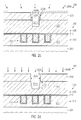
- FIG. 1 a schematically illustrates a cross-sectional view of a semiconductor device 100 at a manufacturing stage in which a complex metallization system 130 is to be formed above a substrate 101 .
- the substrate 101 may comprise a plurality of circuit elements, such as transistors and the like, which may be formed on the basis of design dimensions of approximately 50 nm and less, if sophisticated applications are considered. For convenience, any such circuit elements are not shown in FIG. 1 a .
- the metallization system 130 comprises a metallization layer 110 , which may represent any of a plurality of metallization layers, wherein the number of corresponding metallization layers may depend on the complexity of the circuit layout of the device 100 .
- the metallization layer 110 comprises a dielectric material 111 , which may include a low-k dielectric material in order to reduce the parasitic capacitance between adjacent metal lines 112 , which, at least in the portion shown in FIG. 1 a , may represent closely spaced metal lines as may be required by the overall circuit layout.
- the metal lines 112 may have a width 112 W of approximately 100 nm and less, and the distance between an adjacent two of the metal lines 112 may be of a similar order of magnitude.
- the metal lines may be formed on the basis of a copper material in combination with a conductive barrier material 112 B in order to provide the required copper confinement and the electromigration behavior, as discussed above.
- an dielectric cap or etch stop layer 113 is typically provided on the dielectric material 111 and the metal lines 112 , wherein the cap layer 113 may, depending on the overall process strategy, also provide copper confinement and superior interface characteristics with the metal lines 112 .
- a metallization layer 120 is formed above the layer 110 and comprises a trench 121 T and a via opening 121 V formed in a corresponding dielectric material 121 .
- the dielectric material 121 may represent a low-k dielectric material or any other dielectric material, depending on requirements with respect to parasitic capacitance and the like.
- the trench 121 T may have a significantly greater width 121 W in order to provide sufficient current drive capability, which may be required in the metallization layer 120 .
- the via opening 121 V may connect to one of the metal lines 112 so that a corresponding width 121 U substantially corresponds to the width 112 W of the metal lines 112 in the metallization layer 110 .
- the semiconductor device 100 as illustrated in FIG. 1 a may be formed on the basis of well-established manufacturing techniques. For example, after providing any circuit elements in the device level of the device 100 (not shown), an appropriate contact structure may be provided to connect to the circuit elements and provide a platform for forming thereon the metallization system 130 . Thereafter, one or more metallization layers may be formed on the basis of process techniques as will be described with reference to the metallization layer 120 . Thus, after forming the metallization layer 110 and depositing the cap layer 113 on the basis of well-established deposition techniques, such as chemical vapor deposition (CVD) and the like, in order to provide one or more materials, such as silicon carbide, nitrogen-containing silicon carbide and the like, the dielectric material 121 is deposited.
- CVD chemical vapor deposition
- any appropriate deposition technique may be used, depending on the composition of the material 121 .
- various process strategies are typically used in order to form the via opening 121 U and the trench 121 T according to the design dimensions.
- the via opening 121 V may be formed by providing an etch mask, such as a resist mask, and etching the dielectric material 121 down to a specified depth or down to the etch stop layer 113 .
- a corresponding etch mask for the trench may be formed on the basis of sophisticated lithography techniques, wherein, if required, a corresponding planarization material may be deposited first in order to at least partially fill the via opening 121 V, when extending down to the etch stop layer 113 . Thereafter, a further etch process is performed to obtain the trench 121 T and the etch mask may be removed, while the etch stop layer 113 is also opened so that the via opening 121 V may extend into the metal line 112 . Thereafter, any required manufacturing processes may be performed for preparing the device 100 for the deposition of a conductive barrier material.
- a barrier material 122 B is deposited, for instance, in the form of a tantalum/tantalum nitride layer stack on the basis of sputter deposition and the like.
- a seed material (not shown) may be deposited in order to enhance a subsequent electrochemical deposition process for filling in the copper material into the trench 121 T and the via 121 V. It should be appreciated that, due to the sophisticated device geometries caused by the wide trench 121 T and the narrow via 121 V, corresponding deposition parameters may have to be appropriately selected in order to reliably cover the exposed portions within the trench 121 T and the via 121 V with the barrier material 122 B.
- FIG. 1 b schematically illustrates the semiconductor device 100 when subjected to an electrochemical deposition process for depositing copper material.
- the trench 121 T and the via 121 V may be formed in an interrelated patterning process and the filling thereof may be accomplished on the basis of the common deposition process 102 .
- the sophisticated device topography caused by the per se very complex electrochemical deposition of the copper material may result in deposition irregularities, such as voids 122 C, thereby contributing to significant yield losses and reduced reliability of the resulting metallization system 130 .
- the electrochemical deposition of the copper material 122 A may be based on highly complex electrolyte solutions including sophisticated additives in order to obtain, in combination with an appropriate pulse reverse regime in electroplating techniques, a bottom to top fill behavior.
- a premature “closure” of the via opening 121 V may result in a corresponding irregularity 122 C.
- the probability of creating the deposition-related irregularities 122 C may be reduced by redesigning the layout of the metallization layer 110 so that increased areas are provided at certain portions of the metal lines 112 so as to provide an increased lateral size of the “landing area” of the via 121 V.
- a corresponding redesign may generally reduce overall packing density in the metallization system 130 .
- the present disclosure is directed to various methods and devices that may avoid, or at least reduce, the effects of one or more of the problems identified above.
- the present disclosure provides techniques and semiconductor devices in which the surface topography of a wide trench and a via opening connecting to a metal line of reduced lateral size may be “relaxed” by introducing a pronounced degree of tapering such that a desired reduced lateral width of the via opening may be obtained in the vicinity of the metal line of reduced lateral dimension, while the width of the opening may upwardly increase. Consequently, any constraints imposed on a common deposition process for filling the via opening having the pronounced tapering and the wide trench may be significantly reduced, without requiring dedicated design strategies, which may conventionally result in a reduced packing density.
- the pronounced tapering of the via may be accomplished by modifying the etch sequence for forming the via opening in the dielectric material by increasing a corresponding mask opening in a resist mask at least once during the patterning sequence.
- the resist material may be “eroded” after performing a first etch step and thereafter a further etch step may be performed on the basis of an increased lateral width of the mask opening. If required, further etch steps may be performed with preceding mask erosion processes in order to obtain a substantially gradual tapering of the resulting via opening.
- the etch process for forming the via opening may be performed on the basis of an appropriately designed initial etch mask for forming a first portion of the via opening, while a remaining depth of the via opening may be obtained on the basis of a spacer element, which may also result in a pronounced tapering of the finally obtained via opening.
- One illustrative method disclosed herein comprises forming an etch mask above a dielectric material of a first metallization layer of a semiconductor device, wherein the etch mask comprises a mask opening having a first lateral size that corresponds to a target lateral size at a bottom of a via to be formed in the dielectric material.
- the method further comprises forming a via opening on the basis of the mask opening having the first lateral size in order to form the via opening so as to extend to the first depth in the dielectric material.
- the mask opening is increased to obtain a second lateral size thereof and the via opening is increased on the basis of the mask opening having the second lateral size so as to extend to a second depth.
- the method further comprises forming a trench above the via opening in the dielectric material so as to connect to the via opening.
- the method comprises commonly filling the via opening and the trench with a metal-containing material, wherein the via opening extends to a metal region of a second metallization layer located below the first metallization layer.
- a further illustrative method disclosed herein comprises forming a via opening in a dielectric material of a first metallization layer of a semiconductor device, wherein the via opening extends to a first depth and has a first lateral size. Additionally, a spacer element is formed on sidewalls of the via opening and a depth of the via opening is increased so as to extend to a metal region of a second metallization layer that is formed below the first metallization layer.
- One illustrative semiconductor device disclosed herein comprises a first metallization layer formed above a substrate, wherein the first metallization layer comprises a metal line having a first width.
- the semiconductor device further comprises a second metallization layer formed below the first metallization layer and comprising a second metal line having a second width that is less than the first width.
- the semiconductor device comprises a via extending from the first metal line to the second metal line, wherein the via has a first lateral dimension at the first metal line and has a second lateral dimension at the second metal line, wherein the second lateral dimension is approximately 60% or less of the first lateral dimension.
- FIGS. 1 a - 1 b schematically illustrate cross-sectional views of a sophisticated semiconductor device during various manufacturing stages in forming a metallization system on the basis of conventional process strategies;
- FIGS. 2 a - 2 f schematically illustrate cross-sectional views of a semiconductor device during various manufacturing stages in forming a metallization system, in which a via having a pronounced tapering connects a narrow metal line to a wide metal line, according to illustrative embodiments;
- FIGS. 2 g - 2 i schematically illustrate cross-sectional views of a semiconductor device during various manufacturing stages, in which a pronounced tapering of a via opening may be accomplished by providing an additional spacer element in the patterning sequence, according to further illustrative embodiments.
- the present disclosure relates to manufacturing techniques and corresponding semiconductor devices in which interconnections between narrow metal lines and wide metal lines of adjacent metallization layers may be accomplished on the basis of vias having a pronounced tapering so that a bottom width thereof may be adapted to a design width of the narrow metal line, while the top of the via may have a significantly increased lateral dimension in order to provide enhanced device geometry during a common deposition process for filling the via opening and the corresponding trench of the metal line with a reduced probability of creating deposition-related irregularities.
- transition vias may be provided without requiring specifically provided increased “landing” areas connected to the narrow metal lines, thereby providing enhanced packing density and superior design flexibility in providing complex metallization systems.
- the pronounced tapering of the transition vias may be accomplished by performing the etch sequence for patterning the via opening on the basis of a resist mask, which may intermittently be modified, for instance, by performing one or more material removal processes, so that an initial lateral size of a mask opening may be increased during the further advance of the overall etch sequence.
- the etch sequence for forming the via opening in the dielectric material may be started with a desired lateral size at the top of the via opening and a desired reduced target dimension for the via bottom may be obtained on the basis of a spacer element, which may be formed at an intermediate phase of the overall patterning sequence. Consequently, during the further patterning process, the spacer element may also be removed, so that a corresponding configuration of the spacers may be transferred into the dielectric material, which may thus result in a corresponding tapered configuration. Consequently, a superior device geometry may be provided prior to the common deposition process, thereby not unduly contributing to the overall process complexity, while also avoiding specifically designed contact areas of increased lateral dimensions for the narrow metal lines.
- metal lines having a width of several hundred nanometers and even more may be reliably connected to metal lines of a lower-lying metallization layer having a width of approximately 100 nm and significantly less in sophisticated applications on the basis of an electrochemical deposition process.
- the present disclosure is particularly advantageous in the context of sophisticated metallization systems with metal lines having dimensions in the above-specified range, the principles disclosed herein may nevertheless be applied to any other less critical metallization systems. Consequently, the present disclosure should not be considered as being restricted to any specific device dimensions, unless such restrictions are explicitly set forth in the specification or the appended claims.
- FIGS. 2 a - 2 i further illustrative embodiments will now be described in more detail, wherein reference may also be made to FIGS. 1 a - 1 b if appropriate.
- FIG. 2 a schematically illustrates a cross-sectional view of a semiconductor device 200 comprising a substrate 201 , above which may be formed a metallization system 230 .
- the metallization system 230 may comprise any number of metallization layers wherein, for convenience, a first metallization layer 220 and a second metallization layer 210 are illustrated in FIG. 2 a .
- the metallization system 230 may represent an interconnect structure of a sophisticated semiconductor device, in which circuit elements (not shown) may have critical dimensions of approximately 50 nm and less. As previously explained with reference to the semiconductor device 100 , corresponding circuit elements may be formed in and above an appropriate semiconductor material that may be positioned below the metallization system 230 .
- the metallization layers 210 , 220 may have a similar configuration as is discussed above with reference to the layers 110 , 120 of the device 100 described with reference to FIGS. 1 a - 1 b .
- the metallization layer 210 may comprise a dielectric material 211 , such as a low-k dielectric material and the like, in which may be embedded metal lines 212 , which may represent, at least in the device portion illustrated in FIG. 2 a , metal lines of “narrow pitch.” That is, the metal lines 212 may have a width 212 W which may represent a critical dimension of the metallization layer 210 , which may be approximately 100 nm and less in sophisticated applications.
- the metal lines 212 may have a greater width depending on the overall design rules and the metallization level under consideration.
- an etch stop layer 213 such as a silicon nitride layer, a silicon carbide layer, a nitrogen-enriched silicon carbide layer or any other appropriate material, may be provided with appropriate etch stop capabilities and, if required, corresponding copper confinement characteristics, as previously explained.
- the metallization layer 220 may be provided in the form of a non-patterned dielectric material 221 , which may have any appropriate composition as required for forming therein a wide metal line, at least above the closely spaced metal lines 212 .
- an etch mask 203 for instance in the form of a resist mask, is provided above the dielectric material 221 and comprises a mask opening 203 A having a lateral dimension 203 W that corresponds to a target lateral dimension of a via opening to be formed in the dielectric material 221 .
- the width 203 W may substantially correspond to the width of a corresponding via opening at the bottom thereof so as to enable a reliable connection to one of the metal lines 212 , as indicated by the dashed lines, without interfering with any adjacent metal lines 212 .
- the width 203 W may be substantially equal to or less than the corresponding width 212 W of the metal line 212 .
- the semiconductor device 200 as illustrated in FIG. 2 a may be formed on the basis of process techniques as are also described above with reference to the semiconductor device 100 .
- a high degree of compatibility with conventional process techniques may be accomplished.
- the etch mask 203 may be formed on the basis of well-established process techniques, wherein the mask opening 203 A may, however, be designed to correspond with the width 212 W without requiring additional layers of increased lateral size, which may frequently be used in order to suppress any deposition-related irregularities, such as the irregularities 122 C as illustrated in FIG. 1 b.
- FIG. 2 b schematically illustrates the semiconductor device 200 when exposed to an etch ambient 204 A, which may represent an etch ambient created on the basis of well-established etch recipes. Consequently, during the etch process 204 A, material of the layer 221 may be removed in a highly anisotropic manner, thereby obtaining a via opening 221 V having a lateral size that substantially corresponds to the lateral size 203 W ( FIG. 2 a ) of the mask opening 203 A.
- the etch process 204 A may be controlled so that the depth 221 D of the via opening 221 V may be approximately one third or less of a final depth of the via opening 221 V, that is, a thickness of the dielectric material 221 .
- a corresponding control of the etch process 204 A may be readily accomplished by determining a removal rate for the material 221 and appropriately adjusting the process time of the etch process 204 A.
- FIG. 2 c schematically illustrates the semiconductor device 200 during a material removal process 205 A, which is designed to remove material of the etch mask 203 .
- the process 205 A may be performed as a plasma-assisted process using an oxygen species, while, in other cases, any other appropriate plasma-assisted etch ambient may be used in which organic material may be removed without removing significant portions of the dielectric material 221 .
- the process 205 A may include a wet chemical resist removal process that may be performed on the basis of well-established selective etch chemistries.
- the initial etch mask 203 may be eroded, thereby increasing the lateral size of the opening 203 A, as is indicated by the width 203 E. It should be appreciated that the increased lateral width 203 E may be efficiently adjusted by determining the removal rate of the material of the etch mask 203 in the etch ambient of the process 205 A and controlling the etch time. Due to the selectivity of the etch process 205 A with respect to the dielectric material 221 , the initial lateral width of the via opening 221 V may be substantially maintained, at least at the bottom thereof.
- FIG. 2 d schematically illustrates the semiconductor device 200 during a further etch step 204 B, which may be performed on the basis of the same etch recipe as the process 204 A ( FIG. 2 b ) so that material of the layer 221 may be removed selectively to the etch mask 203 .
- a width of the via opening 221 V may be increased at the top thereof, while also increasing a depth, as indicated by 221 E, wherein, however, a bottom width may substantially correspond to the initial width 203 W ( FIG. 2 c ).
- the anisotropic nature of the etch process 204 B may be less pronounced compared to the process 204 A, thereby obtaining a significant “rounding” of a corner or step caused by the different lateral widths 203 W and 203 E, thereby obtaining a more or less tapered configuration, as illustrated in FIG. 2 d.
- FIG. 2 e schematically illustrates the semiconductor device 200 according to further illustrative embodiments in which an even more pronounced degree of tapering may be accomplished by repeating the processes 205 A, 204 B of FIGS. 2 c - 2 d one or more times, depending on the degree of graduation and the degree of tapering required.
- the device 200 may be exposed to a further resist erosion process 205 B, thereby obtaining a further increased lateral size 203 F of the mask opening 203 A.
- the same or similar process recipes may be used as described above for the process 205 A ( FIG. 2 c ).
- FIG. 2 f schematically illustrates the semiconductor device 200 when exposed to a further etch process 204 C so as to further increase the depth of the via 221 V, wherein, in the embodiment shown, the via 221 V may extend down to the etch stop layer 213 . It should be appreciated, however, that any other depth of the via 221 V may be selected, depending on the overall process strategy. If, for instance, a trench is to be formed in an upper portion of the dielectric material 221 , the final etch step for forming the via opening 221 V may be performed commonly with a corresponding etch step for obtaining the corresponding trench.
- the further processing may be continued by removing the etch mask 203 , which may be accomplished by well-established recipes, and thereafter a further etch mask may be formed so as to define the lateral size of a wide trench to be formed above the via opening 221 V.
- a corresponding film material may be deposited so as to planarize the surface topography and a corresponding etch mask may be formed on the basis of the planarized surface topography using well-established lithography techniques.
- the via opening 221 V and the corresponding wide trench may be filled in a common deposition sequence, as is, for instance, also described with reference to the semiconductor device 100 .
- FIG. 2G schematically illustrates the semiconductor device 200 according to further illustrative embodiments in which a pronounced tapering of a via opening may be obtained on the basis of spacer elements.
- the via opening 221 V may be formed in the dielectric material 221 so as to have an initial width 221 J and having a first depth 221 D, which may, for instance, represent approximately 40-60% of the final depth of the via opening 221 V.
- spacer elements 206 A may be formed on the sidewalls of the via opening 221 V, wherein, in some illustrative embodiments, the spacer element 206 A may be comprised of a material having a similar etch behavior as the dielectric material 221 .
- the removal rate during an etch process designed to remove material of the layer 221 may be within approximately plus/minus 10% for the material of the spacer elements 206 A compared to the dielectric material 221 .
- the spacer element 206 A may be formed on the basis of substantially the same material composition as the dielectric material 221 . In this manner, a substantially identical etch behavior may be accomplished during the further patterning of the via opening 221 V.
- an etch stop liner 206 B such as a silicon dioxide material, a silicon nitride material and the like, may be provided, if required, with a thickness of several nanometers to approximately ten or more nanometers, depending on overall process requirements.
- the semiconductor device 200 as illustrated in FIG. 2 g may be formed on the basis of the following processes.
- an appropriate etch mask such as a resist mask, may be formed, which may comprise an opening having the lateral dimensions corresponding to the initial width 221 J of the via opening 221 V.
- an anisotropic etch process may be performed on the basis of well-established recipes, as also previously discussed, so as to obtain the via opening 221 V extending to the first depth 221 D.
- the resist mask may be removed and a spacer layer (not shown) may be deposited, possibly in combination with the etch stop liner 206 B, which may be accomplished by well-established deposition techniques.
- the spacer material may be etched on the basis of, for instance, similar etch recipes as may also be used for forming the via opening 221 V, due to the similarity of the etch behavior of the spacer material compared to the dielectric material 221 . Consequently, the material of the spacer layer may be removed from horizontal device portions and from the center of the via opening 221 V, wherein the advance of the etch front may be reliably stopped at or within the etch stop liner 206 B, if provided. In this case, a certain degree of “over-etching” may be applied to obtain the pronounced rounding of the spacer elements 206 A at the top of the via opening 221 V.
- exposed portions of the etch stop liner 206 B may be removed, for instance by appropriate selected wet chemical etch recipes, plasma-assisted etch processes and the like.
- the etch stop liner 206 B may be maintained and a corresponding trench etch mask may be formed on the liner 206 B.
- FIG. 2 h schematically illustrates the semiconductor device 200 in a further advanced manufacturing stage.
- an etch mask 207 may be formed above the dielectric material 221 and may comprise an opening 207 A so as to define the position and lateral size of a trench 221 T formed in an upper portion of the dielectric material 221 .
- the trench 221 T may represent a wide metal line having a width 221 W that may be significantly greater than the width 212 W of the metal lines 212 .
- the width 221 W may be twice or more the width 212 W, thereby providing increased current drive capability, as previously explained.
- the etch mask 207 may be formed on the basis of well-established process strategies, in which the surface topography may be planarized, if required, by an appropriate fill material and performing a lithography process for patterning a resist material in accordance with the lateral position and size of the trench 221 T. It should be appreciated that the via opening 221 V may not necessarily be centered in the middle of the trench 221 T so that any appropriate configuration, i.e., spatial relation between the via opening 221 V and the trench 221 T, may be accomplished. Thereafter, the semiconductor device 200 may be exposed to an etch sequence, for instance for removing an exposed portion of any planarization material, if provided, and also etching through exposed portions of the etch stop liner 206 B ( FIG. 2 g ).
- an anisotropic etch process 204 D may be performed to remove material of the layer 221 on the basis of the etch mask 207 , wherein the via opening 221 V is “transferred” into the lower portion of the dielectric material 221 . Due to the presence of the spacer elements 206 A, a pronounced tapering of the via opening 221 V may be accomplished so that a reduced width 221 B at the bottom of the via opening 221 V may be adapted to the width 212 W of the metal line 212 .
- the via opening 221 V may terminate into the trench 221 T with a significantly increased width, which may initially be defined by the width 221 J, wherein it should be appreciated that additional corner rounding may occur during the etch process 204 D, thereby even further increasing the finally obtained width at the top of the via opening 221 V.
- the etch stop liner 206 B FIG. 2 g
- the mask 207 may be removed and the etch stop 213 may be removed in the via opening 221 V in order to expose a surface portion of the metal line 212 .
- a pronounced tapering of the via opening 221 V may be accomplished, thereby providing significantly enhanced surface topography for the subsequent process sequence for forming a conductive barrier layer and filling in copper or any other highly conductive material on the basis of an electrochemical deposition process.
- FIG. 2 i schematically illustrates the semiconductor device 200 in a further advanced manufacturing stage.
- a wide metal line 222 A is formed above a tapered via 221 V, which connects the wide metal line 222 A with one of the metal lines 212 of the lower-lying metallization layer 210 .
- a width 222 W of the wide metal line 222 A may be significantly greater than the width 212 W, thereby providing the high drive current capability of the metal line 222 A.
- a width 222 B of the via 221 V may substantially correspond to the width 212 W of the metal line 212 , thereby enabling a reliable electrical connection without requiring additional contact areas of increased lateral size.
- the width 222 T at the top of the via 221 V may be significantly greater than the bottom width 222 B, thereby providing enhanced surface conditions during the filling process, as previously explained.
- the bottom width 222 B is approximately 60% or less of the top width 222 T.
- the semiconductor device 200 as illustrated in FIG. 2 i may be formed on the basis of well-established process techniques for forming a conductive barrier material 222 A, wherein the enhanced surface topography provided by the pronounced tapering of the corresponding via opening may enhance overall process uniformity and reliability.
- copper material or any other highly conductive metal may be filled in by electrochemical deposition, as previously explained with reference to the device 100 , wherein a reliable bottom-to-top fill behavior may be accomplished irrespective of the significantly increased lateral dimension 222 W compared to the bottom width 222 B.
- any excess material may be removed, for instance by chemical mechanical polishing (CMP), and the further processing may be continued by forming a cap material on the metal line 222 A and the dielectric material 221 .
- CMP chemical mechanical polishing
- the present disclosure provides techniques and semiconductor devices in which a pronounced tapering of transition vias may be accomplished by modifying an etch sequence, for instance by intermittently eroding a resist mask so as to perform two or more etch steps on the basis of a different lateral size of a corresponding mask opening.
- the etch process may start with the “maximum” lateral size of the via opening, which may reduce during the further advance of the etch process on the basis of appropriately dimensioned spacer elements.
Landscapes
- Engineering & Computer Science (AREA)
- Physics & Mathematics (AREA)
- Condensed Matter Physics & Semiconductors (AREA)
- General Physics & Mathematics (AREA)
- Manufacturing & Machinery (AREA)
- Computer Hardware Design (AREA)
- Microelectronics & Electronic Packaging (AREA)
- Power Engineering (AREA)
- Internal Circuitry In Semiconductor Integrated Circuit Devices (AREA)
Priority Applications (4)
| Application Number | Priority Date | Filing Date | Title |
|---|---|---|---|
| JP2011542726A JP2012514319A (ja) | 2008-12-31 | 2009-12-29 | 特別に先細りされた遷移ビアを備えた半導体デバイスのメタライゼーションシステム |
| PCT/EP2009/009308 WO2010076019A1 (en) | 2008-12-31 | 2009-12-29 | A metallization system of a semiconductor device comprising extra-tapered transition vias |
| KR1020117016628A KR20130127013A (ko) | 2008-12-31 | 2009-12-29 | 여분-테이퍼형 전이 비아들을 포함하는 반도체 디바이스의 금속화 시스템 |
| CN200980157543.1A CN102362343B (zh) | 2008-12-31 | 2009-12-29 | 包括非常锥形的转变贯孔的半导体装置的金属化系统 |
Applications Claiming Priority (3)
| Application Number | Priority Date | Filing Date | Title |
|---|---|---|---|
| DE102008063430 | 2008-12-31 | ||
| DE102008063430.1 | 2008-12-31 | ||
| DE102008063430.1A DE102008063430B4 (de) | 2008-12-31 | 2008-12-31 | Verfahren zur Herstellung eines Metallisierungssystem eines Halbleiterbauelements mit zusätzlich verjüngten Übergangskontakten |
Publications (2)
| Publication Number | Publication Date |
|---|---|
| US20100164121A1 US20100164121A1 (en) | 2010-07-01 |
| US8835303B2 true US8835303B2 (en) | 2014-09-16 |
Family
ID=42234624
Family Applications (1)
| Application Number | Title | Priority Date | Filing Date |
|---|---|---|---|
| US12/634,216 Active 2032-04-06 US8835303B2 (en) | 2008-12-31 | 2009-12-09 | Metallization system of a semiconductor device comprising extra-tapered transition vias |
Country Status (6)
| Country | Link |
|---|---|
| US (1) | US8835303B2 (enExample) |
| JP (1) | JP2012514319A (enExample) |
| KR (1) | KR20130127013A (enExample) |
| CN (1) | CN102362343B (enExample) |
| DE (1) | DE102008063430B4 (enExample) |
| WO (1) | WO2010076019A1 (enExample) |
Cited By (3)
| Publication number | Priority date | Publication date | Assignee | Title |
|---|---|---|---|---|
| US20170194229A1 (en) * | 2015-12-30 | 2017-07-06 | Globalfoundries Singapore Pte. Ltd. | Integrated circuits with aluminum via structures and methods for fabricating the same |
| US10825766B2 (en) | 2018-08-07 | 2020-11-03 | Samsung Electronics Co., Ltd. | Semiconductor device with multi-layered wiring and method for fabricating the same |
| US20240324102A1 (en) * | 2021-07-08 | 2024-09-26 | Lg Innotek Co., Ltd. | Circuit board |
Families Citing this family (25)
| Publication number | Priority date | Publication date | Assignee | Title |
|---|---|---|---|---|
| FR2975826A1 (fr) * | 2011-05-27 | 2012-11-30 | St Microelectronics Crolles 2 | Procede de formation d'un trou ou d'une tranchee ayant un profil evase |
| JP2013021001A (ja) * | 2011-07-07 | 2013-01-31 | Renesas Electronics Corp | 半導体装置及び半導体装置の製造方法 |
| US8987916B2 (en) * | 2011-11-28 | 2015-03-24 | Freescale Semiconductor, Inc. | Methods and apparatus to improve reliability of isolated vias |
| JP5891846B2 (ja) * | 2012-02-24 | 2016-03-23 | 富士通セミコンダクター株式会社 | 半導体装置の製造方法 |
| US8815752B2 (en) * | 2012-11-28 | 2014-08-26 | Micron Technology, Inc. | Methods of forming features in semiconductor device structures |
| US9305886B2 (en) * | 2013-12-18 | 2016-04-05 | Globalfoundries Singapore Pte. Ltd. | Integrated circuits having crack-stop structures and methods for fabricating the same |
| US10163778B2 (en) | 2014-08-14 | 2018-12-25 | Taiwan Semiconductor Manufacturing Co., Ltd. | Structure and formation method of damascene structure |
| CN104505471B (zh) * | 2014-12-22 | 2017-12-29 | 昆山工研院新型平板显示技术中心有限公司 | 一种高开口率掩膜板的制备方法及掩膜板 |
| KR20160120891A (ko) | 2015-04-09 | 2016-10-19 | 삼성전자주식회사 | 반도체 장치 |
| US9536826B1 (en) * | 2015-06-15 | 2017-01-03 | Taiwan Semiconductor Manufacturing Co., Ltd. | Fin field effect transistor (finFET) device structure with interconnect structure |
| US9679850B2 (en) * | 2015-10-30 | 2017-06-13 | Taiwan Semiconductor Manufacturing Company Ltd. | Method of fabricating semiconductor structure |
| CN107622992B (zh) | 2016-07-14 | 2021-04-27 | 联华电子股份有限公司 | 半导体元件及其制作方法 |
| US10276485B2 (en) | 2017-08-02 | 2019-04-30 | Taiwan Semiconductor Manufacturing Co., Ltd. | Method for forming a homogeneous bottom electrode via (BEVA) top surface for memory |
| US10998259B2 (en) | 2017-08-31 | 2021-05-04 | Taiwan Semiconductor Manufacturing Company, Ltd. | Semiconductor device and method of manufacture |
| US10522394B2 (en) * | 2017-09-25 | 2019-12-31 | Marvell World Trade Ltd. | Method of creating aligned vias in ultra-high density integrated circuits |
| US10566411B2 (en) * | 2017-12-07 | 2020-02-18 | Globalfoundries Inc. | On-chip resistors with direct wiring connections |
| US11158571B2 (en) * | 2018-12-20 | 2021-10-26 | Micron Technology, Inc. | Devices including conductive interconnect structures, related electronic systems, and related methods |
| WO2020140202A1 (en) * | 2019-01-02 | 2020-07-09 | Yangtze Memory Technologies Co., Ltd. | Method for forming dual damascene interconnect structure |
| CN112151497B (zh) | 2019-06-28 | 2023-08-22 | 台湾积体电路制造股份有限公司 | 半导体结构以及形成半导体结构的方法 |
| DE102019131408B4 (de) | 2019-06-28 | 2025-12-04 | Taiwan Semiconductor Manufacturing Company, Ltd. | Verbesserte Kontaktierung von Metallleitungen bei Fehlausrichtung von BEOL-Durchkontaktierungen |
| US20210020455A1 (en) * | 2019-07-17 | 2021-01-21 | Nanya Technology Corporation | Conductive via structure |
| US11652049B2 (en) | 2021-03-10 | 2023-05-16 | Taiwan Semiconductor Manufacturing Co., Ltd. | Semiconductor device and method of forming thereof |
| KR20230013438A (ko) * | 2021-07-19 | 2023-01-26 | 삼성전자주식회사 | 반도체 장치 |
| KR20230135384A (ko) * | 2022-03-16 | 2023-09-25 | 주식회사 디비하이텍 | 저항 변화 메모리 장치 및 그 제조 방법 |
| US20240332074A1 (en) * | 2023-03-27 | 2024-10-03 | International Business Machines Corporation | Metal wires with expanded sidewalls |
Citations (10)
| Publication number | Priority date | Publication date | Assignee | Title |
|---|---|---|---|---|
| US4902377A (en) | 1989-05-23 | 1990-02-20 | Motorola, Inc. | Sloped contact etch process |
| US6025259A (en) * | 1998-07-02 | 2000-02-15 | Advanced Micro Devices, Inc. | Dual damascene process using high selectivity boundary layers |
| US6239017B1 (en) | 1998-09-18 | 2001-05-29 | Industrial Technology Research Institute | Dual damascene CMP process with BPSG reflowed contact hole |
| US6586329B1 (en) | 1992-11-27 | 2003-07-01 | Mitsubishi Denki Kabshiki Kaisha | Semiconductor device and a method of manufacturing thereof |
| US20030186538A1 (en) | 2002-04-02 | 2003-10-02 | Samsung Electronics Co., Ltd. | Inter-metal dielectric patterns and method of forming the same |
| US6861347B2 (en) * | 2001-05-17 | 2005-03-01 | Samsung Electronics Co., Ltd. | Method for forming metal wiring layer of semiconductor device |
| US7112532B2 (en) * | 2001-07-09 | 2006-09-26 | Texas Instruments Incorporated | Process for forming a dual damascene structure |
| US7179734B2 (en) * | 2003-12-31 | 2007-02-20 | Dongbu Electronics Co., Ltd. | Method for forming dual damascene pattern |
| US20070126121A1 (en) | 2005-12-05 | 2007-06-07 | Taiwan Semiconductor Manufacturing Company, Ltd. | Via structure with improved reliability |
| DE102006025405A1 (de) | 2006-05-31 | 2007-12-06 | Advanced Micro Devices, Inc., Sunnyvale | Metallisierungsschicht eines Halbleiterbauelements mit unterschiedlich dicken Metallleitungen und Verfahren zur Herstellung |
Family Cites Families (13)
| Publication number | Priority date | Publication date | Assignee | Title |
|---|---|---|---|---|
| US4472240A (en) * | 1981-08-21 | 1984-09-18 | Tokyo Shibaura Denki Kabushiki Kaisha | Method for manufacturing semiconductor device |
| US4698128A (en) * | 1986-11-17 | 1987-10-06 | Motorola, Inc. | Sloped contact etch process |
| JPH03257822A (ja) * | 1990-03-07 | 1991-11-18 | Sanyo Electric Co Ltd | 半導体装置の製造方法 |
| JP3427534B2 (ja) * | 1995-01-11 | 2003-07-22 | ソニー株式会社 | 接続孔の形成方法 |
| JPH10163316A (ja) * | 1996-12-04 | 1998-06-19 | Sony Corp | 半導体装置における埋め込み配線の形成方法 |
| TW430943B (en) * | 1999-01-08 | 2001-04-21 | Nippon Electric Co | Method of forming contact or wiring in semiconductor device |
| JP2000260873A (ja) * | 1999-01-08 | 2000-09-22 | Nec Corp | 半導体装置のコンタクト又は配線の形成方法 |
| TW424301B (en) * | 1999-10-02 | 2001-03-01 | Taiwan Semiconductor Mfg | Manufacturing method for dual damascene |
| JP2001358213A (ja) * | 2000-06-13 | 2001-12-26 | Nec Corp | テーパ状スルーホールを有する半導体装置の製造方法 |
| US6440847B1 (en) * | 2001-04-30 | 2002-08-27 | Taiwan Semiconductor Manufacturing Company | Method for forming a via and interconnect in dual damascene |
| KR100386622B1 (ko) * | 2001-06-27 | 2003-06-09 | 주식회사 하이닉스반도체 | 듀얼 다마신 배선 형성방법 |
| JP4476171B2 (ja) * | 2005-05-30 | 2010-06-09 | 富士通マイクロエレクトロニクス株式会社 | 半導体装置の製造方法 |
| JP2007149773A (ja) * | 2005-11-24 | 2007-06-14 | Mitsumi Electric Co Ltd | 半導体装置の製造方法 |
-
2008
- 2008-12-31 DE DE102008063430.1A patent/DE102008063430B4/de active Active
-
2009
- 2009-12-09 US US12/634,216 patent/US8835303B2/en active Active
- 2009-12-29 CN CN200980157543.1A patent/CN102362343B/zh active Active
- 2009-12-29 JP JP2011542726A patent/JP2012514319A/ja active Pending
- 2009-12-29 KR KR1020117016628A patent/KR20130127013A/ko not_active Ceased
- 2009-12-29 WO PCT/EP2009/009308 patent/WO2010076019A1/en not_active Ceased
Patent Citations (10)
| Publication number | Priority date | Publication date | Assignee | Title |
|---|---|---|---|---|
| US4902377A (en) | 1989-05-23 | 1990-02-20 | Motorola, Inc. | Sloped contact etch process |
| US6586329B1 (en) | 1992-11-27 | 2003-07-01 | Mitsubishi Denki Kabshiki Kaisha | Semiconductor device and a method of manufacturing thereof |
| US6025259A (en) * | 1998-07-02 | 2000-02-15 | Advanced Micro Devices, Inc. | Dual damascene process using high selectivity boundary layers |
| US6239017B1 (en) | 1998-09-18 | 2001-05-29 | Industrial Technology Research Institute | Dual damascene CMP process with BPSG reflowed contact hole |
| US6861347B2 (en) * | 2001-05-17 | 2005-03-01 | Samsung Electronics Co., Ltd. | Method for forming metal wiring layer of semiconductor device |
| US7112532B2 (en) * | 2001-07-09 | 2006-09-26 | Texas Instruments Incorporated | Process for forming a dual damascene structure |
| US20030186538A1 (en) | 2002-04-02 | 2003-10-02 | Samsung Electronics Co., Ltd. | Inter-metal dielectric patterns and method of forming the same |
| US7179734B2 (en) * | 2003-12-31 | 2007-02-20 | Dongbu Electronics Co., Ltd. | Method for forming dual damascene pattern |
| US20070126121A1 (en) | 2005-12-05 | 2007-06-07 | Taiwan Semiconductor Manufacturing Company, Ltd. | Via structure with improved reliability |
| DE102006025405A1 (de) | 2006-05-31 | 2007-12-06 | Advanced Micro Devices, Inc., Sunnyvale | Metallisierungsschicht eines Halbleiterbauelements mit unterschiedlich dicken Metallleitungen und Verfahren zur Herstellung |
Non-Patent Citations (1)
| Title |
|---|
| Translation of Official Communication from German Patent Office for German Patent Application No. 10 2008 063 430.1 dated Dec. 4, 2009. |
Cited By (4)
| Publication number | Priority date | Publication date | Assignee | Title |
|---|---|---|---|---|
| US20170194229A1 (en) * | 2015-12-30 | 2017-07-06 | Globalfoundries Singapore Pte. Ltd. | Integrated circuits with aluminum via structures and methods for fabricating the same |
| US9917027B2 (en) * | 2015-12-30 | 2018-03-13 | Globalfoundries Singapore Pte. Ltd. | Integrated circuits with aluminum via structures and methods for fabricating the same |
| US10825766B2 (en) | 2018-08-07 | 2020-11-03 | Samsung Electronics Co., Ltd. | Semiconductor device with multi-layered wiring and method for fabricating the same |
| US20240324102A1 (en) * | 2021-07-08 | 2024-09-26 | Lg Innotek Co., Ltd. | Circuit board |
Also Published As
| Publication number | Publication date |
|---|---|
| DE102008063430A1 (de) | 2010-07-08 |
| DE102008063430B4 (de) | 2016-11-24 |
| KR20130127013A (ko) | 2013-11-22 |
| CN102362343B (zh) | 2015-03-25 |
| US20100164121A1 (en) | 2010-07-01 |
| CN102362343A (zh) | 2012-02-22 |
| WO2010076019A1 (en) | 2010-07-08 |
| JP2012514319A (ja) | 2012-06-21 |
Similar Documents
| Publication | Publication Date | Title |
|---|---|---|
| US8835303B2 (en) | Metallization system of a semiconductor device comprising extra-tapered transition vias | |
| US8048796B2 (en) | Microstructure device including a metallization structure with self-aligned air gaps formed based on a sacrificial material | |
| US8420533B2 (en) | Metallization system of a semiconductor device comprising rounded interconnects formed by hard mask rounding | |
| US8377820B2 (en) | Method of forming a metallization system of a semiconductor device by using a hard mask for defining the via size | |
| US20070077761A1 (en) | Technique for forming a copper-based metallization layer including a conductive capping layer | |
| US8883610B2 (en) | Microstructure device including a metallization structure with self-aligned air gaps between closely spaced metal lines | |
| US7745327B2 (en) | Method of forming a copper-based metallization layer including a conductive cap layer by an advanced integration regime | |
| US7986040B2 (en) | Method of reducing erosion of a metal cap layer during via patterning in semiconductor devices | |
| US20090294898A1 (en) | Microstructure device including a metallization structure with self-aligned air gaps between closely spaced metal lines | |
| US8492269B2 (en) | Hybrid contact structure with low aspect ratio contacts in a semiconductor device | |
| US9379057B2 (en) | Method and structure to reduce the electric field in semiconductor wiring interconnects | |
| US20140264877A1 (en) | Metallization systems of semiconductor devices comprising a copper/silicon compound as a barrier material | |
| US8383510B2 (en) | Semiconductor device comprising metallization layers of reduced interlayer capacitance by reducing the amount of etch stop materials | |
| US20080206986A1 (en) | Method of forming a copper-based metallization layer including a conductive cap layer by an advanced integration regime | |
| US8658494B2 (en) | Dual contact metallization including electroless plating in a semiconductor device | |
| US20100052175A1 (en) | Reducing leakage and dielectric breakdown in dielectric materials of metallization systems of semiconductor devices by forming recesses | |
| US20090108462A1 (en) | Dual integration scheme for low resistance metal layers | |
| US20090294921A1 (en) | Semiconductor device comprising metal lines with a selectively formed dielectric cap layer | |
| US20100289125A1 (en) | Enhanced electromigration performance of copper lines in metallization systems of semiconductor devices by surface alloying | |
| US20100133700A1 (en) | Performance enhancement in metallization systems of microstructure devices by incorporating grain size increasing metal features | |
| US20070178690A1 (en) | Semiconductor device comprising a metallization layer stack with a porous low-k material having an enhanced integrity | |
| US20120153479A1 (en) | Performance Enhancement in Metallization Systems of Microstructure Devices by Incorporating an Intermediate Barrier Layer | |
| US8922023B2 (en) | Semiconductor device comprising metallization layers of reduced interlayer capacitance by reducing the amount of etch stop materials | |
| WO2009134386A1 (en) | Method of reducing erosion of a metal cap layer during via patterning in semiconductor devices | |
| WO2007040860A1 (en) | Technique for forming a copper-based metallization layer including a conductive capping layer |
Legal Events
| Date | Code | Title | Description |
|---|---|---|---|
| AS | Assignment |
Owner name: ADVANCED MICRO DEVICES, INC.,TEXAS Free format text: ASSIGNMENT OF ASSIGNORS INTEREST;ASSIGNORS:FEUSTEL, FRANK;WERNER, THOMAS;FROHBERG, KAI;REEL/FRAME:023629/0294 Effective date: 20090305 Owner name: ADVANCED MICRO DEVICES, INC., TEXAS Free format text: ASSIGNMENT OF ASSIGNORS INTEREST;ASSIGNORS:FEUSTEL, FRANK;WERNER, THOMAS;FROHBERG, KAI;REEL/FRAME:023629/0294 Effective date: 20090305 |
|
| STCF | Information on status: patent grant |
Free format text: PATENTED CASE |
|
| MAFP | Maintenance fee payment |
Free format text: PAYMENT OF MAINTENANCE FEE, 4TH YEAR, LARGE ENTITY (ORIGINAL EVENT CODE: M1551) Year of fee payment: 4 |
|
| MAFP | Maintenance fee payment |
Free format text: PAYMENT OF MAINTENANCE FEE, 8TH YEAR, LARGE ENTITY (ORIGINAL EVENT CODE: M1552); ENTITY STATUS OF PATENT OWNER: LARGE ENTITY Year of fee payment: 8 |