US8779789B2 - Translators coupleable to opposing surfaces of microelectronic substrates for testing, and associated systems and methods - Google Patents
Translators coupleable to opposing surfaces of microelectronic substrates for testing, and associated systems and methods Download PDFInfo
- Publication number
- US8779789B2 US8779789B2 US13/840,937 US201313840937A US8779789B2 US 8779789 B2 US8779789 B2 US 8779789B2 US 201313840937 A US201313840937 A US 201313840937A US 8779789 B2 US8779789 B2 US 8779789B2
- Authority
- US
- United States
- Prior art keywords
- translator
- substrate
- microelectronic substrate
- signal
- microelectronic
- Prior art date
- Legal status (The legal status is an assumption and is not a legal conclusion. Google has not performed a legal analysis and makes no representation as to the accuracy of the status listed.)
- Active
Links
Images


Classifications
-
- G—PHYSICS
- G01—MEASURING; TESTING
- G01R—MEASURING ELECTRIC VARIABLES; MEASURING MAGNETIC VARIABLES
- G01R31/00—Arrangements for testing electric properties; Arrangements for locating electric faults; Arrangements for electrical testing characterised by what is being tested not provided for elsewhere
- G01R31/26—Testing of individual semiconductor devices
-
- G—PHYSICS
- G01—MEASURING; TESTING
- G01R—MEASURING ELECTRIC VARIABLES; MEASURING MAGNETIC VARIABLES
- G01R1/00—Details of instruments or arrangements of the types included in groups G01R5/00 - G01R13/00 and G01R31/00
- G01R1/02—General constructional details
- G01R1/04—Housings; Supporting members; Arrangements of terminals
- G01R1/0408—Test fixtures or contact fields; Connectors or connecting adaptors; Test clips; Test sockets
- G01R1/0416—Connectors, terminals
-
- G—PHYSICS
- G01—MEASURING; TESTING
- G01R—MEASURING ELECTRIC VARIABLES; MEASURING MAGNETIC VARIABLES
- G01R1/00—Details of instruments or arrangements of the types included in groups G01R5/00 - G01R13/00 and G01R31/00
- G01R1/02—General constructional details
- G01R1/06—Measuring leads; Measuring probes
- G01R1/067—Measuring probes
- G01R1/073—Multiple probes
- G01R1/07307—Multiple probes with individual probe elements, e.g. needles, cantilever beams or bump contacts, fixed in relation to each other, e.g. bed of nails fixture or probe card
- G01R1/07364—Multiple probes with individual probe elements, e.g. needles, cantilever beams or bump contacts, fixed in relation to each other, e.g. bed of nails fixture or probe card with provisions for altering position, number or connection of probe tips; Adapting to differences in pitch
- G01R1/07378—Multiple probes with individual probe elements, e.g. needles, cantilever beams or bump contacts, fixed in relation to each other, e.g. bed of nails fixture or probe card with provisions for altering position, number or connection of probe tips; Adapting to differences in pitch using an intermediate adapter, e.g. space transformers
-
- G—PHYSICS
- G01—MEASURING; TESTING
- G01R—MEASURING ELECTRIC VARIABLES; MEASURING MAGNETIC VARIABLES
- G01R31/00—Arrangements for testing electric properties; Arrangements for locating electric faults; Arrangements for electrical testing characterised by what is being tested not provided for elsewhere
- G01R31/28—Testing of electronic circuits, e.g. by signal tracer
- G01R31/2851—Testing of integrated circuits [IC]
- G01R31/2886—Features relating to contacting the IC under test, e.g. probe heads; chucks
- G01R31/2887—Features relating to contacting the IC under test, e.g. probe heads; chucks involving moving the probe head or the IC under test; docking stations
-
- G—PHYSICS
- G01—MEASURING; TESTING
- G01R—MEASURING ELECTRIC VARIABLES; MEASURING MAGNETIC VARIABLES
- G01R31/00—Arrangements for testing electric properties; Arrangements for locating electric faults; Arrangements for electrical testing characterised by what is being tested not provided for elsewhere
- G01R31/28—Testing of electronic circuits, e.g. by signal tracer
- G01R31/282—Testing of electronic circuits specially adapted for particular applications not provided for elsewhere
- G01R31/2831—Testing of materials or semi-finished products, e.g. semiconductor wafers or substrates
-
- H—ELECTRICITY
- H10—SEMICONDUCTOR DEVICES; ELECTRIC SOLID-STATE DEVICES NOT OTHERWISE PROVIDED FOR
- H10W—GENERIC PACKAGES, INTERCONNECTIONS, CONNECTORS OR OTHER CONSTRUCTIONAL DETAILS OF DEVICES COVERED BY CLASS H10
- H10W90/00—Package configurations
- H10W90/701—Package configurations characterised by the relative positions of pads or connectors relative to package parts
- H10W90/721—Package configurations characterised by the relative positions of pads or connectors relative to package parts of bump connectors
- H10W90/724—Package configurations characterised by the relative positions of pads or connectors relative to package parts of bump connectors between a chip and a stacked insulating package substrate, interposer or RDL
Definitions
- the present disclosure relates generally to translators coupleable to opposing surfaces of microelectronic substrates for testing, and associated systems and methods.
- Integrated circuits are typically manufactured in batches. Individual batches typically contain multiple semiconductor wafers or other substrates, within and upon which integrated circuits are formed. Forming the integrated circuits requires a wide variety of semiconductor manufacturing steps, including, for example, depositing, masking, patterning, implanting, etching, planarizing, and other processes.
- Each wafer typically includes hundreds of individual dies which are later separated or singulated and packaged for use. Before the dies are singulated, completed wafers are tested to determine which dies on the wafer are capable of operating according to predetermined specifications. In this manner, integrated circuits that cannot perform as desired are not packaged or otherwise incorporated into finished products.
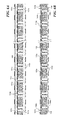
- FIGS. 1A-1C illustrate a representative substrate (e.g., a wafer) having two opposing surfaces, and corresponding translators for electrically accessing the substrate from both surfaces in accordance with an embodiment of the present technology.
- a representative substrate e.g., a wafer having two opposing surfaces, and corresponding translators for electrically accessing the substrate from both surfaces in accordance with an embodiment of the present technology.
- FIG. 1D is a scanning electron micrograph of a portion of a substrate of the type shown in FIGS. 1A-1C .
- FIG. 1E is a partially schematic enlarged illustration of the substrate and two translators shown in FIG. 1C .
- FIG. 2 is a partially schematic, cross-sectional illustration of a substrate and two translators coupled to a tester assembly in accordance with an embodiment of the present disclosure.
- FIGS. 3A and 3B are partially schematic, cross-sectional illustrations of a substrate coupled to two translators that access unpowered dies in accordance with an embodiment of the present technology.
- FIGS. 4A and 4B illustrate a substrate and two translators configured to direct test signals in a radially outward direction in accordance with an embodiment of the present technology.
- FIGS. 5A and 5B illustrate a substrate and two translators positioned to simulate stacked dies of an unsingulated substrate in accordance with an embodiment of the present technology.
- FIGS. 6A and 6B illustrate a substrate and two translators positioned to use the through-substrate vias of incomplete dies in accordance with an embodiment of the present technology.
- FIGS. 7A and 7B illustrate a substrate and two flexible translators configured in accordance with an embodiment of the present technology.
- FIGS. 8A and 8B illustrate a substrate with one rigid translator and one flexible translator configured in accordance with an embodiment of the present technology.
- FIGS. 9A and 9B illustrate a substrate and two rigid translators configured in accordance with an embodiment of the present technology.
- FIGS. 10A and 10B illustrate a substrate and two flexible translators configured in accordance with another embodiment of the present technology.
- a method for testing a microelectronic substrate includes positioning a first translator in a first region proximate to a microelectronic substrate.
- the microelectronic substrate has a first major surface and a second major surface facing away from the first major surface, and electrically conductive through-substrate vias extending through the substrate.
- a first region of the microelectronic substrate extends outwardly from the first major surface of the microelectronic substrate and a second region extends outwardly from the second major surface.
- the method further includes releasably fixing the first translator relative to the microelectronic substrate at the first region; releasably fixing a second translator relative to the microelectronic substrate at the second region while the first translator is fixed relative to the microelectronic substrate at the first region; electrically accessing a first through-substrate via of the microelectronic substrate with the first translator while the first translator is positioned in the first region; and electrically accessing the first through-substrate via or a second through-substrate via of the microelectronic substrate with the second translator while both the first and second translators are releasably fixed relative to the microelectronic substrate.
- the present technology is directed generally to translators coupleable to opposing surfaces of microelectronic substrates, e.g., for testing, and associated systems and methods.
- these techniques can take advantage of through-substrate (e.g., through-wafer or through-silicon) vias to access the microelectronic substrate from both sides and thereby increase the efficiency with which dies of the substrate are tested.
- through-substrate e.g., through-wafer or through-silicon
- FIG. 1A is a partially schematic, cross-sectional illustration of a microelectronic substrate 100 (e.g., a semiconductor wafer) suitable for testing with devices and methods in accordance with the present technology.
- the representative microelectronic substrate 100 includes multiple dies or die sites 101 having corresponding die edges 107 . After testing, the substrate 100 is singulated or diced along the die edges 107 to produce individual dies 101 that are encapsulated or otherwise packaged prior to use.
- Each die 101 can include one or more active areas 102 .
- Dies pads 103 are accessible from a first side (e.g., a first major surface) 106 a of the substrate 100 .
- Through-substrate vias (e.g., through-silicon vias) 104 can provide electrical access to structures within the substrate 100 from both the first side 106 a of the substrate 100 and an oppositely-facing second side (e.g., a second major surface) 106 b .
- Through-substrate via pads 105 provide electrical access to the vias 104 .
- FIG. 1B illustrates a representative substrate 100 positioned between two translators 110 , shown as a first translator 110 a and a second translator 110 b .
- the first translator 110 a is positioned proximate to and facing toward the first side 106 a of the substrate 100
- the second translator 110 b is positioned proximate to and facing toward the second side 106 b of the substrate 100 .
- the term “translator” refers generally to a structure having one or more conductive (e.g., metal) layers, with the translator being temporarily affixed to attached to or engaged with a wafer or other substrate, generally for testing purposes.
- the translator is configured to move with the substrate 100 , e.g., from one station (e.g., a testing or processing station) to another.
- the translator includes one set of contacts having spacings therebetween that match the spacings between the die pads 103 and/or the vias 104 .
- This first set of contacts sometimes referred to generally as wafer contacts or substrate contacts, are engaged with the substrate 100 during testing, and are located on a “wafer side” or “substrate side” of the translator.
- the translator also typically includes a second set of contacts e.g. located on an opposite “tester side” of the translator that may have different spacings, suitable for coupling to a tester or other testing device.
- the translator can provide an interface between the die pads, which are typically very closely spaced together, and the corresponding tester pads, which are typically spaced further apart.
- the translators can be temporarily attached to the substrate via vacuum forces, clamps, and/or other techniques so as to move with the substrate 100 from one station to another during testing, pre-testing and/or post-testing procedures.
- the substrate or wafer contacts of the first translator 110 a can include first conductors 111 positioned to contact the die pads 103 of the associated substrate 100 , and second conductors 112 positioned to contact the through-substrate vias 104 (e.g., the via pads 105 ) at the first side 106 a of the substrate 100 .
- the second translator 110 b can also include second conductors 112 positioned to contact the through-substrate vias 104 from the second side 106 b of the substrate 100 .
- the first translator 110 a can access the through-substrate vias 104 from the first side 106 a
- the second translator 110 b can access the same or different through-substrate vias 104 from the second side 106 b.
- FIG. 1C illustrates the substrate 100 with the first and second translators 110 a , 110 b releasably attached to it.
- the substrate 100 can be tested with electrical signals that access both the first and second sides 106 a , 106 b of the substrate 100 .
- the first translator 110 a is positioned in a first region 108 a that extends outwardly from the first major surface 106 a of the substrate 100
- the second translator 110 b is positioned in a second region 108 b that extends outwardly from the second major surface 106 b of the substrate 100 .
- FIG. 1D is a scanning electron micrograph illustrating a portion of the substrate 100 shown in FIG. 1C . Accordingly, FIG. 1D illustrates individual dies 101 and associated through-substrate vias 104 .
- FIG. 1E is an enlarged illustration of a portion of the substrate 100 and the translators 110 a , 110 b shown in FIG. 1C .
- FIG. 2 is a partially schematic, cross-sectional illustration of a representative substrate 100 and representative translators 110 a , 110 b arranged for testing in accordance with an embodiment of the present technology.
- the arrangement can include a tester assembly 120 that in turn includes multiple testers or test modules 121 .
- the testers 121 can include first testers 121 a positioned to access the first translator 110 a , and second testers 121 b positioned to access the substrate 100 via the second translator 110 b .
- the first testers 121 a can communicate electrically with first tester contacts 113 a carried by the first translator 110 a
- the second testers 121 b can access the second translator 110 b through second tester contacts 113 b .
- Tester signal paths 122 connect or provide communication between the first testers 121 a and the second testers 121 b . Accordingly, tests performed by the first testers 121 a can be coordinated with tests performed by the second testers 121 b .
- This function can be particularly useful for testing certain microelectronic devices, e.g., NAND devices, for which results from one test can direct which of multiple possible follow-on tests are conducted.
- Another advantage of the foregoing arrangement is that it can be used to test a die that ultimately is incorporated into a stack of dies.
- Such dies may use the through-substrate vias 104 to transmit different signals to pads located at the first side 106 a than to pads located at the second side 106 b .
- the first and second testers 121 a , 121 b can be programmed/configured to deliver and/or respond to the different signals that the dies 101 may generate.
- the second testers 121 b can simulate a lower die, and the first testers 121 a can simulate an upper die.
- signals transmitted to and/or from the dies 101 through the through-substrate vias 104 can, in operation, travel in only one direction (e.g., toward only the first translator 110 a or toward only the second translator 110 b ).
- Representative devices include diodes and tri-state devices. Accordingly, the ability to access both ends of individual through-substrate vias 104 can increase the versatility of the overall testing operation.
- the through-substrate via of one die can be used to facilitate testing of another die, as will be described further below.
- signals are transmitted in both directions along one or more vias. For example, such signals can be used to test the integrity of unidirectional devices (which should transmit signals in only one direction) and/or test the ability of multi-directional devices to transmit signals in multiple directions.
- FIGS. 3A and 3B illustrate a representative substrate 100 with representative first and second translators 110 a , 110 b configured in accordance with a particular embodiment of the present technology.
- the translators 110 a , 110 b and a set of first testers 121 a are shown schematically in position for engaging the substrate 100 .
- the first and second translators 110 a , 110 b have been engaged with the substrate 100
- the first testers 121 a have been engaged with the first translator 110 a .
- the second translator 110 b includes circuitry that allows the through-substrate vias of an unpowered or untested die to facilitate testing of a powered or test die (e.g., a die or device under test, or “DUT”).
- a powered or test die e.g., a die or device under test, or “DUT”.
- FIG. 3B illustrates a first die 101 a (also identified as “Die 4 Test”) that is powered and under test, and is located between two second die 101 b (also identified as “Unpowered Die 3 ” and “Unpowered Die 5 ”) that are unpowered.
- a corresponding first tester 121 a accesses the first die 101 a by first through-substrate vias 104 a of the first die 101 a .
- the second translator 110 b includes second signal paths 114 b that connect the first through-substrate vias 104 a of the first die with second through-substrate vias 104 b of the second dies 101 b . Accordingly, the first tester 121 a can communicate with the first die 101 a by first signal paths 114 a that pass through both the first through-substrate vias 104 a of the first die 101 a , and the second through-substrate vias 104 b of the second dies 101 b .
- This arrangement can be used to increase the access available to each die that is currently under test by using adjacent (and/or other) dies that are not currently under test.
- this arrangement can allow the first testers 121 a to evaluate signals from the first die 101 a that are typically transmitted unidirectionally “down” through the first through-substrate vias 104 a toward the second translator 110 b by using the second translator 110 b to redirect such signals back up through the second vias 104 b of the second dies 101 b to the first testers 121 a .
- all the dies can be tested by sequentially shifting the first testers 121 a and/or connections between the testers and the dies 101 a , 101 b .
- the second vias 104 b can be used to send instructions between the first and second translators 110 a , 110 b.
- FIGS. 4A and 4B illustrate another arrangement in which a second translator 110 b is used to convey signals that may be conveyed to and/or received from components not shown in FIGS. 4A and 4B .
- the first testers 121 a can communicate with the dies 101 as indicated by the first signal paths 114 a
- a second translator 110 b can convey signals away, for example to/from additional testers (offsite or distributed testers) that are not visible in FIGS. 4A and 4B , as indicated by second signal paths 114 b .
- the signals can be routed along paths that extend beyond the outer periphery of the substrate 100 , as will be described further below with reference to FIGS. 7A and 7B .
- FIGS. 5A and 5B illustrate an arrangement in which the first and second translators 110 a , 110 b include signal paths that are used to test multiple unsingulated dies in a manner that emulates a stacked die arrangement.
- a total of six dies 101 a - 101 f are involved in a particular test that simulates three stacked dies.
- the first, third and fifth dies 101 a , 101 c , 101 e are powered and tested.
- the second, fourth, and sixth dies 101 b , 101 d , 101 f are unpowered, but provide pathways to connect the powered dies.
- each of the translators 110 a , 110 b are configured to use the unpowered dies to route signals from the bottom of one tested die to the top of the other, thus emulating a stacked die arrangement.
- first signal paths 114 a at the first translator 110 a provide communication between a first tester 121 a and the first die 101 a .
- Second signal paths 114 b at the second translator 110 b connect the through-substrate vias 104 of the first die 101 a to the through-substrate vias 104 of the second die 101 b .
- Third signal paths 114 c at the first translator 101 a connect the through-substrate vias 104 of the second, unpowered die 101 b with the through-substrate vias 104 of the third, powered die 101 c .
- a similar arrangement is used to connect the third die 101 c with the fifth die 101 e , and route signals to a second tester 121 b .
- aspects of the operation of the dies that are typically evident only when the dies are in a stacked arrangement can be tested before the dies are singulated and actually placed in a stacked arrangement. Although individual dies may be tested together in a simulated stacked arrangement, once singulated, the dies do not necessarily need to be stacked with the same dies used during the simulation.
- FIGS. 6A and 6B illustrate an arrangement for testing dies (e.g., complete, intact dies) by using the through-substrate vias of incomplete dies carried by the substrate 100 .
- the outer periphery of the substrate 100 can include portions of incomplete or partial dies 101 b .
- These incomplete dies 101 b may have undergone at least some of the manufacturing processes associated with complete dies 101 a , for example, the formation of through-substrate vias.
- the complete dies 101 a can have first through-substrate vias 104 a and the incomplete dies 101 b can have second through-substrate vias 104 b .
- the second through-substrate vias 104 b can be used to provide access to first dies 101 a by using the second translator 110 b to convey signals along signal paths 114 between the second through-substrate vias 104 b of partial or incomplete dies 101 b and the first through-substrate vias 104 a of complete dies 101 a . Accordingly, the second vias 104 b can provide a “pass-through” function.
- FIGS. 7A and 7B illustrate a configuration in which a representative substrate 100 is tested by relatively thin first and second translators 110 a , 110 b .
- the second translator 110 b can have an “edge extended” configuration that includes edge extensions 115 extending beyond the periphery of the substrate 100 .
- the edge extensions 115 can provide additional functional areas e.g., for coupling to testers and/or other external devices.
- the translators 110 a , 110 b can be formed from thin, flexible layered metal/dielectric materials to provide for low clearance in a vertical direction. Accordingly, this arrangement is particularly suitable where the vertical clearance requirements during testing are tight.
- FIGS. 8A and 8B illustrate another arrangement in which a representative substrate 100 is positioned between a first translator 810 a having a relatively thick configuration, and a second translator 810 b having a thin configuration generally similar to that described above with reference to FIGS. 7A and 7B .
- This arrangement can be used where vertical clearance above the substrate 100 is not as tight or critical as the vertical clearance below the substrate 100 .
- FIGS. 9A and 9B illustrate another arrangement in which a substrate 100 is positioned between two translators 910 a , 910 b , both of which have a relatively thick configuration. This arrangement can be used in installations for which vertical clearance both above and below the substrate 100 is not as tight or critical.
- FIGS. 10A and 10B illustrate a substrate 100 positioned between first and second translators 1010 a , 1010 b , both of which are relatively thin, and neither of which include the edge extender arrangement described above with reference to FIGS. 7A and 7B . Accordingly, this arrangement can be used in instances for which the communications to and from the substrate 100 do not require a density of signal paths and/or other features that necessitate or otherwise require an edge extender.
- a representative method includes positioning a first translator in a first region proximate to a microelectronic substrate.
- the microelectronic substrate has a first major surface and a second major surface facing away from the first major surface, and has electrically conductive through-substrate vias extending through the substrate, with a first region extending outwardly from the first major surface of the microelectronic substrate and a second region extending outwardly from the second major surface.
- the method can further include releasably fixing the first translator relative to the microelectronic substrate at the first region, releasably fixing a second translator relative to the microelectronic substrate at the second region while the first translator is fixed relative to the microelectronic substrate at the first region, electrically accessing a first through-substrate via of the microelectronic substrate with the first translator while the first translator is positioned in the first region, and electrically accessing the first through-substrate via or a second through-substrate via of the microelectronic substrate with the second translator while both the first and second translators are fixed relative to the microelectronic substrate.
- the method further includes simultaneously electrically accessing the microelectronic substrate with both the first and second translators. In still further particular embodiments, the method further includes receiving a first signal from the first translator at the second translator, and in response, directing the first signal or a second signal to the microelectronic substrate or the first translator.
- the first via is part of a first die
- the method further includes simulating stacked dies by routing a signal from the first translator through the first via of the first die to the second translator, using the second translator to route the signal from the first via to a second via, receiving the signal from the second via at the first translator, and using first translator to route the signal from the second via to a third via of the microelectronic substrate, the third via being part of a second die different than the first die.
- the methods disclosed herein include and encompass, in addition to methods of making and using the disclosed devices and systems, methods of instructing others to make and use the disclosed devices and systems. Accordingly, any and all methods of use and manufacture disclosed herein also fully disclose and enable corresponding methods of instructing such methods of use and manufacture. Methods of instructing such use and manufacture may take the form of computer-readable-medium-based executable programs or processes.
- translators having configurations other than those expressly described above can be used to provide access to substrates from opposing surfaces of the substrates.
- Substrates can be tested in a generally horizontal orientation, as shown in the Figures, or in a vertical or other orientation in other embodiments.
- the same signal received by one translator from another is transmitted directly to another site, e.g., back to the first translator, or to a die under test.
- the received signal is altered before further transmission, or provides a basis for transmission of a different signal.
Landscapes
- Physics & Mathematics (AREA)
- General Physics & Mathematics (AREA)
- Engineering & Computer Science (AREA)
- General Engineering & Computer Science (AREA)
- Computer Hardware Design (AREA)
- Microelectronics & Electronic Packaging (AREA)
- Power Engineering (AREA)
- Testing Or Measuring Of Semiconductors Or The Like (AREA)
- Tests Of Electronic Circuits (AREA)
Priority Applications (9)
| Application Number | Priority Date | Filing Date | Title |
|---|---|---|---|
| US13/840,937 US8779789B2 (en) | 2012-04-09 | 2013-03-15 | Translators coupleable to opposing surfaces of microelectronic substrates for testing, and associated systems and methods |
| EP13776186.2A EP2837023A4 (en) | 2012-04-09 | 2013-04-04 | COMPARATIVE SURFACES OF MICROELECTRONIC SUBSTRATES COUPLED TRANSLATORS FOR TESTING AND CORRESPONDING SYSTEMS AND METHODS |
| JP2015505804A JP6058119B2 (ja) | 2012-04-09 | 2013-04-04 | テスト用マイクロエレクトロニクス基板の両面に結合可能なトランスレータ、ならびに関連するシステムおよび方法 |
| KR1020147031469A KR20150007305A (ko) | 2012-04-09 | 2013-04-04 | 테스트를 하기 위한 마이크로 전자 기판들의 대향하는 표면들에 결합가능한 트랜슬레이터들, 및 관련 시스템들과 방법들 |
| CN201380030314.XA CN104350588B (zh) | 2012-04-09 | 2013-04-04 | 可连接到微电子基板的相反表面的用于测试的转换器以及相关的系统和方法 |
| PCT/US2013/035286 WO2013154909A1 (en) | 2012-04-09 | 2013-04-04 | Translators coupleable to opposing surfaces of microelectronic substrates for testing, and associated systems and methods |
| SG11201406383RA SG11201406383RA (en) | 2012-04-09 | 2013-04-04 | Translators coupleable to opposing surfaces of microelectronic substrates for testing, and associated systems and methods |
| TW102112402A TWI551869B (zh) | 2012-04-09 | 2013-04-08 | 用於測試之可耦接至微電子基板之相對表面的傳送器及相關聯系統及方法 |
| US14/309,672 US9222965B2 (en) | 2012-04-09 | 2014-06-19 | Translators coupleable to opposing surfaces of microelectronic substrates for testing, and associated systems and methods |
Applications Claiming Priority (2)
| Application Number | Priority Date | Filing Date | Title |
|---|---|---|---|
| US201261621954P | 2012-04-09 | 2012-04-09 | |
| US13/840,937 US8779789B2 (en) | 2012-04-09 | 2013-03-15 | Translators coupleable to opposing surfaces of microelectronic substrates for testing, and associated systems and methods |
Related Child Applications (1)
| Application Number | Title | Priority Date | Filing Date |
|---|---|---|---|
| US14/309,672 Continuation US9222965B2 (en) | 2012-04-09 | 2014-06-19 | Translators coupleable to opposing surfaces of microelectronic substrates for testing, and associated systems and methods |
Publications (2)
| Publication Number | Publication Date |
|---|---|
| US20130265071A1 US20130265071A1 (en) | 2013-10-10 |
| US8779789B2 true US8779789B2 (en) | 2014-07-15 |
Family
ID=49291807
Family Applications (2)
| Application Number | Title | Priority Date | Filing Date |
|---|---|---|---|
| US13/840,937 Active US8779789B2 (en) | 2012-04-09 | 2013-03-15 | Translators coupleable to opposing surfaces of microelectronic substrates for testing, and associated systems and methods |
| US14/309,672 Active US9222965B2 (en) | 2012-04-09 | 2014-06-19 | Translators coupleable to opposing surfaces of microelectronic substrates for testing, and associated systems and methods |
Family Applications After (1)
| Application Number | Title | Priority Date | Filing Date |
|---|---|---|---|
| US14/309,672 Active US9222965B2 (en) | 2012-04-09 | 2014-06-19 | Translators coupleable to opposing surfaces of microelectronic substrates for testing, and associated systems and methods |
Country Status (8)
| Country | Link |
|---|---|
| US (2) | US8779789B2 (https=) |
| EP (1) | EP2837023A4 (https=) |
| JP (1) | JP6058119B2 (https=) |
| KR (1) | KR20150007305A (https=) |
| CN (1) | CN104350588B (https=) |
| SG (1) | SG11201406383RA (https=) |
| TW (1) | TWI551869B (https=) |
| WO (1) | WO2013154909A1 (https=) |
Cited By (1)
| Publication number | Priority date | Publication date | Assignee | Title |
|---|---|---|---|---|
| US20150015299A1 (en) * | 2012-04-09 | 2015-01-15 | Advanced Inquiry Systems, Inc. | Translators coupleable to opposing surfaces of microelectronic substrates for testing, and associated systems and methods |
Families Citing this family (4)
| Publication number | Priority date | Publication date | Assignee | Title |
|---|---|---|---|---|
| FR3032038B1 (fr) | 2015-01-27 | 2018-07-27 | Soitec | Procede, dispositif et systeme de mesure d'une caracteristique electrique d'un substrat |
| CN106154596A (zh) * | 2015-04-08 | 2016-11-23 | 上海纪显电子科技有限公司 | 光电显示装置、检测装置及其方法 |
| US9794009B1 (en) * | 2016-06-30 | 2017-10-17 | Litepoint Corporation | Method for testing a radio frequency (RF) data packet signal transceiver for proper implicit beamforming operation |
| US11791326B2 (en) * | 2021-05-10 | 2023-10-17 | International Business Machines Corporation | Memory and logic chip stack with a translator chip |
Citations (21)
| Publication number | Priority date | Publication date | Assignee | Title |
|---|---|---|---|---|
| US4628991A (en) | 1984-11-26 | 1986-12-16 | Trilogy Computer Development Partners, Ltd. | Wafer scale integrated circuit testing chuck |
| US5567654A (en) | 1994-09-28 | 1996-10-22 | International Business Machines Corporation | Method and workpiece for connecting a thin layer to a monolithic electronic module's surface and associated module packaging |
| US5592730A (en) | 1994-07-29 | 1997-01-14 | Hewlett-Packard Company | Method for fabricating a Z-axis conductive backing layer for acoustic transducers using etched leadframes |
| US5629838A (en) | 1993-06-24 | 1997-05-13 | Polychip, Inc. | Apparatus for non-conductively interconnecting integrated circuits using half capacitors |
| US6100709A (en) | 1998-05-29 | 2000-08-08 | Intel Corporation | Silicon wafer testing rig and a method for testing a silicon wafer wherein the silicon wafer is bent into a dome shape |
| US6121065A (en) | 1997-09-26 | 2000-09-19 | Institute Of Microelectronics | Wafer scale burn-in testing |
| US6429513B1 (en) | 2001-05-25 | 2002-08-06 | Amkor Technology, Inc. | Active heat sink for cooling a semiconductor chip |
| US6737879B2 (en) | 2001-06-21 | 2004-05-18 | Morgan Labs, Llc | Method and apparatus for wafer scale testing |
| US6798224B1 (en) | 1997-02-11 | 2004-09-28 | Micron Technology, Inc. | Method for testing semiconductor wafers |
| US6853205B1 (en) | 2003-07-17 | 2005-02-08 | Chipmos Technologies (Bermuda) Ltd. | Probe card assembly |
| US6897666B2 (en) | 2002-12-31 | 2005-05-24 | Intel Corporation | Embedded voltage regulator and active transient control device in probe head for improved power delivery and method |
| US6982869B2 (en) | 2001-03-21 | 2006-01-03 | Micron Technology, Inc. | Folded interposer |
| US7148715B2 (en) * | 2004-06-02 | 2006-12-12 | Micron Technology, Inc. | Systems and methods for testing microelectronic imagers and microfeature devices |
| US7245507B2 (en) | 1999-07-15 | 2007-07-17 | Dibene Ii Joseph T | Method and apparatus for providing power to a microprocessor with integrated thermal and EMI management |
| WO2008011106A2 (en) | 2006-07-18 | 2008-01-24 | Octavian Scientific, Inc. | Methods and apparatus for flexible extension of electrical conductors beyond the edges of a substrate |
| US20080309349A1 (en) | 2007-06-15 | 2008-12-18 | Computer Access Technology Corporation | Flexible interposer system |
| US7649245B2 (en) | 2005-05-04 | 2010-01-19 | Sun Microsystems, Inc. | Structures and methods for a flexible bridge that enables high-bandwidth communication |
| US7671449B2 (en) | 2005-05-04 | 2010-03-02 | Sun Microsystems, Inc. | Structures and methods for an application of a flexible bridge |
| US7855341B2 (en) | 2002-12-18 | 2010-12-21 | Micron Technology, Inc. | Methods and apparatus for a flexible circuit interposer |
| US20120074976A1 (en) * | 2010-09-28 | 2012-03-29 | Advanced Inquiry Systems, Inc. | Wafer testing systems and associated methods of use and manufacture |
| US8363418B2 (en) | 2011-04-18 | 2013-01-29 | Morgan/Weiss Technologies Inc. | Above motherboard interposer with peripheral circuits |
Family Cites Families (23)
| Publication number | Priority date | Publication date | Assignee | Title |
|---|---|---|---|---|
| US7349223B2 (en) * | 2000-05-23 | 2008-03-25 | Nanonexus, Inc. | Enhanced compliant probe card systems having improved planarity |
| US7952373B2 (en) * | 2000-05-23 | 2011-05-31 | Verigy (Singapore) Pte. Ltd. | Construction structures and manufacturing processes for integrated circuit wafer probe card assemblies |
| US6680213B2 (en) * | 2001-04-02 | 2004-01-20 | Micron Technology, Inc. | Method and system for fabricating contacts on semiconductor components |
| US6841991B2 (en) * | 2002-08-29 | 2005-01-11 | Micron Technology, Inc. | Planarity diagnostic system, E.G., for microelectronic component test systems |
| JP2006010682A (ja) * | 2004-05-28 | 2006-01-12 | Jsr Corp | 回路基板の検査装置および回路基板の検査方法 |
| US7489147B2 (en) * | 2004-07-15 | 2009-02-10 | Jsr Corporation | Inspection equipment of circuit board and inspection method of circuit board |
| JP4598779B2 (ja) * | 2004-11-16 | 2010-12-15 | 富士通セミコンダクター株式会社 | コンタクタ及びコンタクタを用いた試験方法 |
| CN101248363B (zh) * | 2005-08-23 | 2012-01-18 | 日本电气株式会社 | 半导体器件、半导体芯片、芯片间互连测试方法以及芯片间互连切换方法 |
| CN101346813A (zh) * | 2005-12-22 | 2009-01-14 | Jsr株式会社 | 晶片检查用电路基板装置、探针卡和晶片检查装置 |
| US7821283B2 (en) * | 2005-12-22 | 2010-10-26 | Jsr Corporation | Circuit board apparatus for wafer inspection, probe card, and wafer inspection apparatus |
| JP5005321B2 (ja) * | 2006-11-08 | 2012-08-22 | パナソニック株式会社 | 半導体装置 |
| US7791174B2 (en) * | 2008-03-07 | 2010-09-07 | Advanced Inquiry Systems, Inc. | Wafer translator having a silicon core isolated from signal paths by a ground plane |
| KR101214036B1 (ko) * | 2008-10-28 | 2012-12-20 | 가부시키가이샤 어드밴티스트 | 시험 장치 및 회로 모듈 |
| KR101046382B1 (ko) * | 2008-12-30 | 2011-07-05 | 주식회사 하이닉스반도체 | 웨이퍼의 반도체 칩 테스트 장치 |
| US8988090B2 (en) * | 2009-04-21 | 2015-03-24 | Johnstech International Corporation | Electrically conductive kelvin contacts for microcircuit tester |
| US7977956B2 (en) * | 2009-04-28 | 2011-07-12 | Formfactor, Inc. | Method and apparatus for probe card alignment in a test system |
| US8344749B2 (en) * | 2010-06-07 | 2013-01-01 | Texas Instruments Incorporated | Through carrier dual side loop-back testing of TSV die after die attach to substrate |
| US8471577B2 (en) * | 2010-06-11 | 2013-06-25 | Texas Instruments Incorporated | Lateral coupling enabled topside only dual-side testing of TSV die attached to package substrate |
| US8648615B2 (en) * | 2010-06-28 | 2014-02-11 | Xilinx, Inc. | Testing die-to-die bonding and rework |
| US8952711B2 (en) * | 2011-10-20 | 2015-02-10 | Taiwan Semiconductor Manufacturing Company, Ltd. | Methods for probing semiconductor wafers |
| US8952713B1 (en) * | 2012-02-08 | 2015-02-10 | Altera Corporation | Method and apparatus for die testing |
| US9391447B2 (en) * | 2012-03-06 | 2016-07-12 | Intel Corporation | Interposer to regulate current for wafer test tooling |
| US8779789B2 (en) * | 2012-04-09 | 2014-07-15 | Advanced Inquiry Systems, Inc. | Translators coupleable to opposing surfaces of microelectronic substrates for testing, and associated systems and methods |
-
2013
- 2013-03-15 US US13/840,937 patent/US8779789B2/en active Active
- 2013-04-04 EP EP13776186.2A patent/EP2837023A4/en not_active Withdrawn
- 2013-04-04 KR KR1020147031469A patent/KR20150007305A/ko not_active Ceased
- 2013-04-04 CN CN201380030314.XA patent/CN104350588B/zh active Active
- 2013-04-04 JP JP2015505804A patent/JP6058119B2/ja active Active
- 2013-04-04 WO PCT/US2013/035286 patent/WO2013154909A1/en not_active Ceased
- 2013-04-04 SG SG11201406383RA patent/SG11201406383RA/en unknown
- 2013-04-08 TW TW102112402A patent/TWI551869B/zh active
-
2014
- 2014-06-19 US US14/309,672 patent/US9222965B2/en active Active
Patent Citations (23)
| Publication number | Priority date | Publication date | Assignee | Title |
|---|---|---|---|---|
| US4628991A (en) | 1984-11-26 | 1986-12-16 | Trilogy Computer Development Partners, Ltd. | Wafer scale integrated circuit testing chuck |
| US5629838A (en) | 1993-06-24 | 1997-05-13 | Polychip, Inc. | Apparatus for non-conductively interconnecting integrated circuits using half capacitors |
| US5592730A (en) | 1994-07-29 | 1997-01-14 | Hewlett-Packard Company | Method for fabricating a Z-axis conductive backing layer for acoustic transducers using etched leadframes |
| US5567654A (en) | 1994-09-28 | 1996-10-22 | International Business Machines Corporation | Method and workpiece for connecting a thin layer to a monolithic electronic module's surface and associated module packaging |
| US6798224B1 (en) | 1997-02-11 | 2004-09-28 | Micron Technology, Inc. | Method for testing semiconductor wafers |
| US6121065A (en) | 1997-09-26 | 2000-09-19 | Institute Of Microelectronics | Wafer scale burn-in testing |
| US6100709A (en) | 1998-05-29 | 2000-08-08 | Intel Corporation | Silicon wafer testing rig and a method for testing a silicon wafer wherein the silicon wafer is bent into a dome shape |
| US7245507B2 (en) | 1999-07-15 | 2007-07-17 | Dibene Ii Joseph T | Method and apparatus for providing power to a microprocessor with integrated thermal and EMI management |
| US6982869B2 (en) | 2001-03-21 | 2006-01-03 | Micron Technology, Inc. | Folded interposer |
| US6429513B1 (en) | 2001-05-25 | 2002-08-06 | Amkor Technology, Inc. | Active heat sink for cooling a semiconductor chip |
| US6836130B2 (en) | 2001-06-21 | 2004-12-28 | Morgan T. Johnson | Method and apparatus for wafer scale testing |
| US6737879B2 (en) | 2001-06-21 | 2004-05-18 | Morgan Labs, Llc | Method and apparatus for wafer scale testing |
| US7855341B2 (en) | 2002-12-18 | 2010-12-21 | Micron Technology, Inc. | Methods and apparatus for a flexible circuit interposer |
| US6897666B2 (en) | 2002-12-31 | 2005-05-24 | Intel Corporation | Embedded voltage regulator and active transient control device in probe head for improved power delivery and method |
| US6853205B1 (en) | 2003-07-17 | 2005-02-08 | Chipmos Technologies (Bermuda) Ltd. | Probe card assembly |
| US7148715B2 (en) * | 2004-06-02 | 2006-12-12 | Micron Technology, Inc. | Systems and methods for testing microelectronic imagers and microfeature devices |
| US7649245B2 (en) | 2005-05-04 | 2010-01-19 | Sun Microsystems, Inc. | Structures and methods for a flexible bridge that enables high-bandwidth communication |
| US7671449B2 (en) | 2005-05-04 | 2010-03-02 | Sun Microsystems, Inc. | Structures and methods for an application of a flexible bridge |
| WO2008011106A2 (en) | 2006-07-18 | 2008-01-24 | Octavian Scientific, Inc. | Methods and apparatus for flexible extension of electrical conductors beyond the edges of a substrate |
| US7572132B2 (en) | 2006-07-18 | 2009-08-11 | Advanced Inquiry Systems, Inc. | Methods and apparatus for flexible extension of electrical conductors beyond the edges of a substrate |
| US20080309349A1 (en) | 2007-06-15 | 2008-12-18 | Computer Access Technology Corporation | Flexible interposer system |
| US20120074976A1 (en) * | 2010-09-28 | 2012-03-29 | Advanced Inquiry Systems, Inc. | Wafer testing systems and associated methods of use and manufacture |
| US8363418B2 (en) | 2011-04-18 | 2013-01-29 | Morgan/Weiss Technologies Inc. | Above motherboard interposer with peripheral circuits |
Non-Patent Citations (2)
| Title |
|---|
| International Preliminary Report on Patentability for PCT/US2007/016379 issued Jan. 20, 2009. |
| International Search Report and Written Opinion of the International Search Authority for PCT/US2007/016379 mailed Oct. 14, 2008. |
Cited By (2)
| Publication number | Priority date | Publication date | Assignee | Title |
|---|---|---|---|---|
| US20150015299A1 (en) * | 2012-04-09 | 2015-01-15 | Advanced Inquiry Systems, Inc. | Translators coupleable to opposing surfaces of microelectronic substrates for testing, and associated systems and methods |
| US9222965B2 (en) * | 2012-04-09 | 2015-12-29 | Translarity, Inc. | Translators coupleable to opposing surfaces of microelectronic substrates for testing, and associated systems and methods |
Also Published As
| Publication number | Publication date |
|---|---|
| EP2837023A1 (en) | 2015-02-18 |
| WO2013154909A1 (en) | 2013-10-17 |
| KR20150007305A (ko) | 2015-01-20 |
| US9222965B2 (en) | 2015-12-29 |
| TW201350880A (zh) | 2013-12-16 |
| SG11201406383RA (en) | 2014-11-27 |
| EP2837023A4 (en) | 2016-01-13 |
| CN104350588B (zh) | 2017-04-05 |
| US20150015299A1 (en) | 2015-01-15 |
| JP2015514226A (ja) | 2015-05-18 |
| JP6058119B2 (ja) | 2017-01-11 |
| CN104350588A (zh) | 2015-02-11 |
| US20130265071A1 (en) | 2013-10-10 |
| TWI551869B (zh) | 2016-10-01 |
Similar Documents
| Publication | Publication Date | Title |
|---|---|---|
| US9222965B2 (en) | Translators coupleable to opposing surfaces of microelectronic substrates for testing, and associated systems and methods | |
| KR101384714B1 (ko) | 반도체 검사장치 | |
| CN106664812B (zh) | 用于产生模块化堆叠式集成电路的系统及方法 | |
| US6537831B1 (en) | Method for selecting components for a matched set using a multi wafer interposer | |
| EP2324499B1 (en) | Circuit for the parallel supplying of power during testing of a plurality of electronic devices integrated on a semiconductor wafer | |
| CN106663645B (zh) | 用于在测试设备中传输信号的同轴结构 | |
| KR20080058343A (ko) | 싱귤레이션된 다이를 테스트하는 장치 및 방법 | |
| KR20160087820A (ko) | 장치와 테스터 사이에서 신호를 전송하는 인터커넥트 | |
| US7459924B2 (en) | Apparatus for providing electrical access to one or more pads of the wafer using a wafer translator and a gasket | |
| US6815712B1 (en) | Method for selecting components for a matched set from a wafer-interposer assembly | |
| KR101442354B1 (ko) | 예비 공간 변환기 및 이를 이용하여 제조된 공간 변환기, 그리고 상기 공간 변환기를 구비하는 반도체 소자 검사 장치 | |
| US6483330B1 (en) | Method for selecting components for a matched set using wafer interposers | |
| US20220365132A1 (en) | Test board and test apparatus including the same | |
| KR101431915B1 (ko) | 예비 공간 변환기 및 이를 이용하여 제조된 공간 변환기, 그리고 상기 공간 변환기를 구비하는 반도체 소자 검사 장치 | |
| US6259263B1 (en) | Compliant contactor for testing semiconductors | |
| US8802454B1 (en) | Methods of manufacturing a semiconductor structure | |
| US20140253165A1 (en) | Probe card | |
| KR20210105313A (ko) | Dut 맵이 서로 다른 반도체 테스터와 핸들러 사이의 인터페이싱을 위한 장치 및 이를 포함하는 반도체 테스트 장비 | |
| CN114295868B (zh) | 堆叠芯片与堆叠芯片的测试方法 | |
| US9230682B2 (en) | Method and system for automated device testing | |
| US20020075023A1 (en) | Method for electrically testing a wafer interposer | |
| US11804413B1 (en) | Product design for test to enable electrical non-destructive test for measuring multi-chip interconnect defects | |
| US20080232074A1 (en) | Circuit Card Assembly Including Individually Testable Layers |
Legal Events
| Date | Code | Title | Description |
|---|---|---|---|
| STCF | Information on status: patent grant |
Free format text: PATENTED CASE |
|
| AS | Assignment |
Owner name: ADVANCED INQUIRY SYSTEMS, INC., OREGON Free format text: ASSIGNMENT OF ASSIGNORS INTEREST;ASSIGNOR:JOHNSON, MORGAN T.;REEL/FRAME:036710/0792 Effective date: 20120511 Owner name: TRANSLARITY, INC., CALIFORNIA Free format text: CHANGE OF NAME;ASSIGNOR:ADVANCED INQUIRY SYSTEMS, INC.;REEL/FRAME:036745/0587 Effective date: 20141117 |
|
| MAFP | Maintenance fee payment |
Free format text: PAYMENT OF MAINTENANCE FEE, 4TH YR, SMALL ENTITY (ORIGINAL EVENT CODE: M2551) Year of fee payment: 4 |
|
| MAFP | Maintenance fee payment |
Free format text: PAYMENT OF MAINTENANCE FEE, 8TH YR, SMALL ENTITY (ORIGINAL EVENT CODE: M2552); ENTITY STATUS OF PATENT OWNER: SMALL ENTITY Year of fee payment: 8 |
|
| MAFP | Maintenance fee payment |
Free format text: PAYMENT OF MAINTENANCE FEE, 12TH YR, SMALL ENTITY (ORIGINAL EVENT CODE: M2553); ENTITY STATUS OF PATENT OWNER: SMALL ENTITY Year of fee payment: 12 |