US8735962B2 - Semiconductor device and method of manufacturing the same - Google Patents
Semiconductor device and method of manufacturing the same Download PDFInfo
- Publication number
- US8735962B2 US8735962B2 US13/599,680 US201213599680A US8735962B2 US 8735962 B2 US8735962 B2 US 8735962B2 US 201213599680 A US201213599680 A US 201213599680A US 8735962 B2 US8735962 B2 US 8735962B2
- Authority
- US
- United States
- Prior art keywords
- layer
- gate
- layers
- conductive
- semiconductor device
- Prior art date
- Legal status (The legal status is an assumption and is not a legal conclusion. Google has not performed a legal analysis and makes no representation as to the accuracy of the status listed.)
- Active, expires
Links
- 239000004065 semiconductor Substances 0.000 title claims abstract description 70
- 238000004519 manufacturing process Methods 0.000 title description 14
- 239000000758 substrate Substances 0.000 claims abstract description 30
- 239000000463 material Substances 0.000 claims description 123
- 229910052710 silicon Inorganic materials 0.000 claims description 59
- 239000010703 silicon Substances 0.000 claims description 59
- 229910052751 metal Inorganic materials 0.000 claims description 37
- 239000002184 metal Substances 0.000 claims description 37
- 229910021332 silicide Inorganic materials 0.000 claims description 18
- FVBUAEGBCNSCDD-UHFFFAOYSA-N silicide(4-) Chemical compound [Si-4] FVBUAEGBCNSCDD-UHFFFAOYSA-N 0.000 claims description 18
- 229910021420 polycrystalline silicon Inorganic materials 0.000 claims description 3
- 229920005591 polysilicon Polymers 0.000 claims description 3
- 239000010410 layer Substances 0.000 abstract description 503
- 239000011229 interlayer Substances 0.000 abstract description 61
- XUIMIQQOPSSXEZ-UHFFFAOYSA-N Silicon Chemical compound [Si] XUIMIQQOPSSXEZ-UHFFFAOYSA-N 0.000 description 54
- 238000000034 method Methods 0.000 description 22
- 239000012535 impurity Substances 0.000 description 21
- 150000004767 nitrides Chemical class 0.000 description 12
- ZOXJGFHDIHLPTG-UHFFFAOYSA-N Boron Chemical compound [B] ZOXJGFHDIHLPTG-UHFFFAOYSA-N 0.000 description 11
- OKTJSMMVPCPJKN-UHFFFAOYSA-N Carbon Chemical compound [C] OKTJSMMVPCPJKN-UHFFFAOYSA-N 0.000 description 11
- 229910052796 boron Inorganic materials 0.000 description 11
- 229910052799 carbon Inorganic materials 0.000 description 11
- VYPSYNLAJGMNEJ-UHFFFAOYSA-N Silicium dioxide Chemical compound O=[Si]=O VYPSYNLAJGMNEJ-UHFFFAOYSA-N 0.000 description 10
- 238000005530 etching Methods 0.000 description 10
- 229910052814 silicon oxide Inorganic materials 0.000 description 10
- 239000011810 insulating material Substances 0.000 description 6
- 239000004020 conductor Substances 0.000 description 5
- 230000010354 integration Effects 0.000 description 4
- 230000008878 coupling Effects 0.000 description 3
- 238000010168 coupling process Methods 0.000 description 3
- 238000005859 coupling reaction Methods 0.000 description 3
- 238000000151 deposition Methods 0.000 description 3
- 229920002120 photoresistant polymer Polymers 0.000 description 3
- 238000010586 diagram Methods 0.000 description 2
- 230000014759 maintenance of location Effects 0.000 description 2
- 238000000059 patterning Methods 0.000 description 2
- 238000004891 communication Methods 0.000 description 1
- 238000013500 data storage Methods 0.000 description 1
- 230000003247 decreasing effect Effects 0.000 description 1
- 230000000694 effects Effects 0.000 description 1
- 238000002347 injection Methods 0.000 description 1
- 239000007924 injection Substances 0.000 description 1
- 238000009413 insulation Methods 0.000 description 1
- 239000011159 matrix material Substances 0.000 description 1
- 239000000203 mixture Substances 0.000 description 1
- 239000002356 single layer Substances 0.000 description 1
- 239000007787 solid Substances 0.000 description 1
- WFKWXMTUELFFGS-UHFFFAOYSA-N tungsten Chemical compound [W] WFKWXMTUELFFGS-UHFFFAOYSA-N 0.000 description 1
- 229910052721 tungsten Inorganic materials 0.000 description 1
- 239000010937 tungsten Substances 0.000 description 1
Images


Classifications
-
- H—ELECTRICITY
- H10—SEMICONDUCTOR DEVICES; ELECTRIC SOLID-STATE DEVICES NOT OTHERWISE PROVIDED FOR
- H10B—ELECTRONIC MEMORY DEVICES
- H10B41/00—Electrically erasable-and-programmable ROM [EEPROM] devices comprising floating gates
- H10B41/20—Electrically erasable-and-programmable ROM [EEPROM] devices comprising floating gates characterised by three-dimensional arrangements, e.g. with cells on different height levels
- H10B41/23—Electrically erasable-and-programmable ROM [EEPROM] devices comprising floating gates characterised by three-dimensional arrangements, e.g. with cells on different height levels with source and drain on different levels, e.g. with sloping channels
- H10B41/27—Electrically erasable-and-programmable ROM [EEPROM] devices comprising floating gates characterised by three-dimensional arrangements, e.g. with cells on different height levels with source and drain on different levels, e.g. with sloping channels the channels comprising vertical portions, e.g. U-shaped channels
-
- H—ELECTRICITY
- H01—ELECTRIC ELEMENTS
- H01L—SEMICONDUCTOR DEVICES NOT COVERED BY CLASS H10
- H01L21/00—Processes or apparatus adapted for the manufacture or treatment of semiconductor or solid state devices or of parts thereof
- H01L21/70—Manufacture or treatment of devices consisting of a plurality of solid state components formed in or on a common substrate or of parts thereof; Manufacture of integrated circuit devices or of parts thereof
- H01L21/77—Manufacture or treatment of devices consisting of a plurality of solid state components or integrated circuits formed in, or on, a common substrate
- H01L21/78—Manufacture or treatment of devices consisting of a plurality of solid state components or integrated circuits formed in, or on, a common substrate with subsequent division of the substrate into plural individual devices
- H01L21/82—Manufacture or treatment of devices consisting of a plurality of solid state components or integrated circuits formed in, or on, a common substrate with subsequent division of the substrate into plural individual devices to produce devices, e.g. integrated circuits, each consisting of a plurality of components
- H01L21/822—Manufacture or treatment of devices consisting of a plurality of solid state components or integrated circuits formed in, or on, a common substrate with subsequent division of the substrate into plural individual devices to produce devices, e.g. integrated circuits, each consisting of a plurality of components the substrate being a semiconductor, using silicon technology
- H01L21/8232—Field-effect technology
- H01L21/8234—MIS technology, i.e. integration processes of field effect transistors of the conductor-insulator-semiconductor type
- H01L21/823487—MIS technology, i.e. integration processes of field effect transistors of the conductor-insulator-semiconductor type with a particular manufacturing method of vertical transistor structures, i.e. with channel vertical to the substrate surface
-
- H—ELECTRICITY
- H01—ELECTRIC ELEMENTS
- H01L—SEMICONDUCTOR DEVICES NOT COVERED BY CLASS H10
- H01L29/00—Semiconductor devices adapted for rectifying, amplifying, oscillating or switching, or capacitors or resistors with at least one potential-jump barrier or surface barrier, e.g. PN junction depletion layer or carrier concentration layer; Details of semiconductor bodies or of electrodes thereof ; Multistep manufacturing processes therefor
- H01L29/66—Types of semiconductor device ; Multistep manufacturing processes therefor
- H01L29/68—Types of semiconductor device ; Multistep manufacturing processes therefor controllable by only the electric current supplied, or only the electric potential applied, to an electrode which does not carry the current to be rectified, amplified or switched
- H01L29/76—Unipolar devices, e.g. field effect transistors
- H01L29/772—Field effect transistors
- H01L29/78—Field effect transistors with field effect produced by an insulated gate
- H01L29/788—Field effect transistors with field effect produced by an insulated gate with floating gate
- H01L29/7889—Vertical transistors, i.e. transistors having source and drain not in the same horizontal plane
-
- H—ELECTRICITY
- H10—SEMICONDUCTOR DEVICES; ELECTRIC SOLID-STATE DEVICES NOT OTHERWISE PROVIDED FOR
- H10B—ELECTRONIC MEMORY DEVICES
- H10B41/00—Electrically erasable-and-programmable ROM [EEPROM] devices comprising floating gates
- H10B41/20—Electrically erasable-and-programmable ROM [EEPROM] devices comprising floating gates characterised by three-dimensional arrangements, e.g. with cells on different height levels
Definitions
- Example embodiments of the present invention relate to a semiconductor device and a method of manufacturing the same, more particularly, to a three-dimensional floating gate NAND flash memory device and a method of manufacturing the same.
- a semiconductor device may include memory cells that are arranged in two dimensions on a semiconductor substrate.
- the integration of memory cells has been increased by reducing memory cell size within a predetermined area of a semiconductor substrate in order to achieve a high level of integration of a semiconductor device.
- a reduction in the size of memory cells is reaching physical limits.
- a semiconductor device having a three-dimensional structure in which memory cells are arranged in three dimensions has been developed.
- a three-dimensional structured semiconductor device can efficiently utilize the area of a semiconductor substrate and improve the degree of integration as compared with a semiconductor device that has memory cells arranged in two dimensions.
- a stack structure is formed of a plurality of conductive layers and a plurality of interlayer insulating layers are alternately stacked one upon another on a semiconductor substrate, a vertical hole that passes through the stack structure is formed, and a charge trap layer and a channel layer are formed in the vertical hole.
- the charge trap layer is formed on a sidewall of the vertical hole, while the vertical hole having the charge trap layer therein is filled with the channel layer.
- the charge trap layer is a SiN layer capable of trapping electric charge.
- the above-described conventional three-dimensional NAND flash memory device has Silicon-Oxide-Nitride-Oxide-Silicon (SONOS) memory cells formed at intersections between channel layers and conductive layers.
- SONOS Silicon-Oxide-Nitride-Oxide-Silicon
- a SONOS memory cell has a deteriorated data retention characteristic and a lower erase speed in comparison with a floating-gate memory cell. Therefore, there is a need for a three-dimensional NAND flash memory device that has floating-gate memory cells with improved operating characteristics of a three-dimensional semiconductor device.
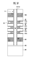
- FIG. 1 is a cross-sectional view of a conventional floating gate type three-dimensional NAND flash memory device.
- the floating gate type three-dimensional NAND flash memory device includes a vertical channel layer 121 ; a tunnel insulating layer 119 formed on a sidewall of the vertical channel layer 121 ; a plurality of control gates CG stacked one upon another in a direction in which the vertical channel layer 121 extends and separated from each other with interlayer insulating layers 105 a , 105 b , 105 c , 105 d , and 105 e interposed therebetween; floating gates FG formed between the plurality of control gates CG and covering the vertical channel layer 121 with the tunnel insulating layer 119 interposed therebetween; and a dielectric layer 115 formed between the floating gates FG and the control gates CG.
- the plurality of control gates CG are formed by patterning a plurality of first conductive layers 107 a , 107 b , 107 c , and 107 d stacked one upon another and separated from each other with the interlayer insulating layers 105 a , 105 b , 105 c , 105 d , and 105 e interposed therebetween, respectively.
- the first conductive layers 107 a , 107 b , 107 c , and 107 d may be silicon layers.
- the dielectric layer 115 is formed along the surface of a vertical hole and the surface of a recessed region that extends from the vertical hole to the plurality of interlayer insulating layers 105 a , 105 b , 105 c , 105 d , and 105 e .
- the vertical hole is formed by etching the plurality of first conductive layers 107 a , 107 b , 107 c , and 107 d and the plurality of interlayer insulating layers 105 a , 105 b , 105 c , 105 d , and 105 e .
- the recessed region is formed by etching the plurality of interlayer insulating layers 105 a , 105 b , 105 c , 105 d , and 105 e exposed through the vertical hole after the vertical hole is formed.
- sidewalls of the plurality of first conductive layers 107 a , 107 b , 107 c , and 107 d adjacent to the vertical hole protrude further than those of the plurality of interlayer insulating layers 105 a , 105 b , 105 c , 105 d , and 105 e.
- the floating gates FG are formed by filling the recessed regions with a second conductive layer 117 after the dielectric layer 115 is formed.
- the second conductive layer 117 may be a silicon layer.
- the tunnel insulating layer 119 is formed on the sidewall of the vertical hole including sidewalls of the floating gates FG after the floating gates FG are formed.
- the tunnel insulating layer 119 has a thickness that allows electrons to pass by the tunnel effect when voltage having a predetermined level or higher is applied between the vertical channel layer 121 and the floating gates FG.
- the vertical channel layer 121 may be formed by filling the vertical hole with a semiconductor material, such as silicon, after the tunnel insulating layer 119 is formed.
- Memory cells are formed at intersections between the floating gates FG and the vertical channel layer 121 .
- the memory cells are coupled in series in the direction in which the vertical channel layer 121 extends, thereby forming strings.
- the above-described semiconductor device controls the voltage applied to the vertical channel layer 121 and the control gates CG to thereby accumulate charges on the floating gates FG.
- a program bias having a higher level than the voltage of the vertical channel layer 121 is applied to a pair of control gates CG_ 1 and CG_ 2 disposed over and under the selected floating gate FG_ 1 . Electrons are thereby injected into the selected floating gate FG_ 1 to increase a threshold voltage of a selected memory cell.
- the program bias may cause undesirable injection of electrons into unselected floating gate FG_ 2 and FG_ 3 adjacent to the pair of control gates CG_ 1 and CG_ 2 .
- a disturbance phenomenon occurs, that is, a threshold voltage of each of the unselected memory cells disposed over and under the selected memory cell changes.
- Each of the memory cells of the conventional floating gate type three-dimensional NAND flash memory device is driven by two control gates CG stacked one upon another. Therefore, in order to form the memory cells constituting the strings, two more control gates CG than the number of floating gates FG need to be stacked. Further, because the two control gates used to drive a particular memory cell are shared by another memory cell disposed over or under the particular memory cell, operating conditions for driving the particular memory cell is complicated.
- Example embodiments relate to a floating gate type three-dimensional semiconductor device including a floating-gate memory cell coupled to a single control gate and a method of manufacturing the same.
- a semiconductor device includes a vertical channel layer protruding upward from a semiconductor substrate, a tunnel insulating layer covering a sidewall of the vertical channel layer, a plurality of floating gates separated from each other and stacked one upon another along the vertical channel layer, and surrounding the vertical channel layer with the tunnel insulating layer interposed therebetween, a plurality of control gates enclosing the plurality of floating gates, respectively, and an interlayer insulating layer provided between the plurality of control gates.
- a method of manufacturing a semiconductor device includes stacking layer stacks alternating with third material layers, the layer stacks each having first material layers and a second material layer stacked between the first material layers, forming a vertical hole passing through the layer stacks and the third material layers stacked alternately with each other, forming a first recessed region by etching the second material layer exposed through the vertical hole, forming a floating gate which fills the first recessed region, forming a tunnel insulating layer along a sidewall of the vertical hole and a sidewall of the floating gate, and forming a vertical channel layer which fills the vertical hole.
- FIG. 1 is a cross-sectional view of a conventional floating gate type three-dimensional NAND flash memory device
- FIG. 2 is a perspective view of a semiconductor device according to an embodiment of the present invention.
- FIG. 3 is a schematic view of a portion of a memory cell of the semiconductor device of FIG. 2 ;
- FIGS. 4A to 4H are cross-sectional views of the semiconductor device taken along line I-I′ of FIG. 2 according to an embodiment of the present invention and illustrating a method of manufacturing the same according to a first embodiment of the present invention
- FIGS. 5A to 5H are cross-sectional views illustrating a method of manufacturing a semiconductor device according to a second embodiment of the present invention.
- FIGS. 6A to 6D are cross-sectional views illustrating a method of manufacturing a semiconductor device according to a third embodiment of the present invention.
- FIG. 7 is a schematic block diagram of a memory system according to an embodiment of the present invention.
- a three-dimensional floating-gate NAND flash memory device and a method of manufacturing the same according to embodiments of the present invention that can reduce disturbance, reduce the size of a semiconductor device and simplify operating conditions of memory cells in comparison with the conventional floating gate type three-dimensional NAND flash memory device will now be described.
- FIG. 2 is a perspective view of a semiconductor device according to an embodiment of the present invention.
- FIG. 2 particularly illustrates a three-dimensional NAND flash memory device that has a lower select transistor, a plurality of memory cells, and an upper select transistor stacked one upon another in a sequential manner on a semiconductor substrate.
- interlayer insulating layers are not depicted.
- the semiconductor device includes a common source region 203 , a plurality of bit lines 229 , and a plurality of memory strings ST disposed between the common source region 203 and the bit lines 229 .
- the common source region 203 is a doped silicon layer that is formed on a semiconductor substrate 201 or an impurity-implanted region that is formed by implanting impurities into the semiconductor substrate 201 .
- the plurality of memory strings ST that form memory blocks may be commonly coupled to an upper part of the common source region 203 .
- the bit lines 229 are conductive patterns that are separated from the semiconductor substrate 201 and are disposed above the semiconductor substrate 201 .
- the bit lines 229 are arranged next to each other and separated from each other. For example, the bit lines 229 extend in the x-direction of an xyz coordinate system.
- the plurality of memory strings ST are coupled to each of the bit lines 229 .
- Each of the memory strings ST includes an upper select transistor UST, a lower select transistor LST and the plurality of memory cells MC that are coupled in series with each other along the vertical channel layer 221 .
- the lower select transistor LST is coupled to the common source region 203
- the upper select transistor UST is coupled to one of the bit lines 229
- the plurality of memory cells MC are disposed between the lower select transistor LST and the upper select transistor UST.
- the vertical channel layer 221 extends in the z-direction perpendicular to the semiconductor substrate 201 and protrudes upward from the semiconductor substrate 201 .
- the semiconductor device according to an embodiment of the present invention further includes a tunnel insulating layer 219 that is formed to cover at least a sidewall of the vertical channel layer 221 .
- the tunnel insulating layer 219 may have a thickness that allows electrons to pass by voltage having a predetermined level being applied to control gates CG of the memory cells MC.
- a plurality of floating gates FG of the memory cells MC are separated from each other and stacked one upon another along the vertical channel layer 221 .
- the floating gates FG are stacked in the z-direction along the vertical channel layer 221 .
- FIG. 3 is a schematic view of a portion of the memory cell of the semiconductor device shown in FIG. 2 .
- FIG. 3 shows only the vertical channel layer 221 , the floating gate FG and the control gate CG.
- the floating gate FG covers, encircles and/or surrounds the vertical channel layer 221 .
- the tunnel insulating layer 219 is formed between the floating gate FG and the vertical channel layer 221 .
- the floating gate FG is surrounded, enveloped and/or enclosed by the control gate CG.
- the semiconductor device further includes a dielectric layer 215 that is formed between the floating gates FG and the control gates CG.
- the dielectric layer 215 may be further formed on the surfaces of the tunnel insulating layer 219 not surrounded by the control gate CG.
- the dielectric layer 215 may have such a large thickness that the dielectric layer 215 can insulate the floating gates FG and the control gates CG of the memory cell MC from each other.
- the control gates CG of the memory cells MC cover the top and bottom surfaces and sidewall of the floating gates FG, respectively, with the dielectric layer 215 interposed therebetween.
- the control gates CG are separated from each other and stacked one upon another in the z-direction along the vertical channel layer 221 .
- the control gates CG each may be split by slits into memory block units and be in the form of plates.
- Each of the control gates CG includes a pair of first conductive layers 207 and a second conductive layer 209 interposed between the first conductive layers 207 .
- each of the control gates CG may include first conductive layers 207 disposed over and under one of the floating gates FG while interposing the floating gate.
- the second conductive layer 209 may have a greater thickness than the first conductive layer 207 .
- the floating gate FG is formed in a recessed region of the second conductive layer 209 between the first conductive layers 207 .
- the second conductive layer 209 may cover a sidewall of the floating gate FG between the first conductive layers 207 .
- the floating gate FG is embedded in the control gate CG.
- each of the control gates CG may be a single conductive layer that covers each of the floating gates FG.
- the first and second conductive layers 207 and 209 may be formed of different materials having an etch selectivity therebetween so as to allow for a selective etch of any one of the first and second conductive layers 207 and 209 .
- the first conductive layer 207 may be a doped silicon layer
- the second conductive layer 209 may be an undoped silicon layer.
- the first conductive layer 207 may be an undoped silicon layer
- the second conductive layer 209 may be a doped silicon layer.
- the doped silicon layer may be a layer doped with impurities such as boron or carbon.
- the second conductive layer 209 may be a silicon layer, or a metal layer or a metal silicide layer having lower resistance than a silicon layer.
- the conductive layer of each of the control gates CG may include a metal layer or a metal silicide layer having lower resistance than a silicon layer.
- a first select gate LSG which is a gate of the lower select transistor LST, is disposed between and separated from the plurality of control gates CG and the common source region 203 .
- the first select gate LSG covers, encircles and/or surrounds the vertical channel layer 221 with a gate insulating layer 218 a interposed therebetween.
- the first select gate LSG may have an etch selectivity with respect to the second conductive layer 209 such that the first select gate LSG cannot be removed during a selective etch process of the second conductive layer 209 .
- the first select gate LSG may be formed of the same material as the first conductive layer 207 .
- the first select gate LSG may be formed of a doped silicon layer doped with impurities such as boron or carbon, an undoped silicon layer, a metal layer or a metal silicide layer.
- the first select gate LSG may be formed of the same conductive material as the control gate CG.
- the first select gate LSG may be split into memory block units and be in the form of plates.
- a second select gate USG which is a gate of the upper select transistor UST, is separated from and disposed between the bit line 229 and the plurality of control gates CG stacked one upon another.
- the second select gate USG covers, encircles, and/or surrounds the vertical channel layer 221 with a gate insulating layer 218 b interposed therebetween.
- the second select gate USG may have an etch selectivity with respect to the second conductive layer 209 such that the second conductive layer 209 is not removed during a selective etch process of the second conductive layer 209 .
- the second select gate USG may be formed of the same material as the first conductive layer 207 .
- the second select gate USG may be formed of a doped silicon layer doped with impurities such as boron or carbon, an undoped silicon layer, a metal layer or a metal silicide layer.
- the second select gate USG and the control gate CG may be formed of the same conductive material as each other.
- the second select gate USG may be in the form of a line that extends in a direction crossing the bit lines 229 .
- bit line contact plug 225 is further formed between the bit line 229 and the vertical channel layer 221 so as to establish a connection between the bit line 229 and the memory string ST.
- the bit line 229 and the vertical channel layer 221 may come in direct contact with each other. In this case, the bit line contact plug 225 may be removed.
- each of the floating gates FG is covered by the dielectric layer 215 and embedded in each of the control gates CG. Therefore, the semiconductor device according to an embodiment of the present invention applies a program bias to a single control gates CG covering a selected floating gate FG in order to perform a program operation that injects electrons into the selected floating gate FG. Therefore, according to an embodiment of the present invention, program operation conditions can be simplified in comparison with the conventional floating gate type three-dimensional NAND flash memory device that injects electrons into a selected floating gate by a program bias being applied to two control gates.
- each of the floating gates FG is not formed between the neighboring control gates CG, but is instead embedded in each of the control gates CG, so that the distances between the plurality of control gates CG can be appropriately designed to reduce disturbance. Therefore, according to an embodiment of the present invention, a change in the threshold voltage of an unselected floating gate caused by a program bias applied to a selected control gate covering the selected floating gate can be avoided.
- each of the memory cells MC is driven by a single control gate CG. Therefore, in an embodiment of the present invention, the number of control gates CG stacked one upon another can be reduced as compared with the conventional floating gate type three-dimensional NAND flash memory device that includes memory cells each driven by two control gates. Accordingly, in an embodiment of the present invention, the size of the semiconductor device can be reduced.
- the floating gate FG includes a top surface, a bottom surface and a sidewall that face the control gate CG.
- the sidewall of the conventional floating gate as shown in FIG. 1 does not face the control gate. Therefore, in an embodiment of the present invention, capacitance between the sidewall of the floating gate FG and the control gate CG can be better utilized as compared with that of the conventional floating gate type three-dimensional NAND flash memory device. That is, a coupling ratio between the control gate CG and the floating gate FG with respect to the floating gate FG of the same size is higher in an embodiment of the present invention than in the conventional floating gate type three-dimensional NAND flash memory device.
- the coupling ratio between the control gate CG and the floating gate FG can be increased, so that the size of the semiconductor device can be reduced by reducing the width of the floating gate FG.
- an operating voltage used to perform program and erase operations of memory cells can be reduced.
- FIGS. 4A to 4H are cross-sectional views of the semiconductor device taken along line I-I′ of FIG. 2 to illustrate a method of manufacturing the same according to a first embodiment.
- a stack structure ML is formed on the semiconductor substrate 201 including the common source region 203 .
- the stack structure ML may include a first stack structure ML 1 , a second stack structure ML 2 and a third stack structure ML 3 that are stacked in a sequential manner.
- the semiconductor substrate 201 may further include a well structure implanted with impurities.
- the common source region 203 may be formed by implanting impurities into the semiconductor substrate 201 or depositing a doped silicon layer onto the semiconductor substrate 201 .
- N type impurities may be implanted into the common source region 203 .
- the first stack structure ML 1 includes a first interlayer insulating layer 205 a , the conductive layer 207 a for the first select gate (LSG) and the second interlayer insulating layer 205 b that are stacked one upon another on the semiconductor substrate 201 including the common source region 203 .
- the first and second interlayer insulating layers 205 a and 205 b insulate the conductive layer 207 a for the first select gate from the common source region 203 and the lowermost control gate conductive layer CG 1 .
- the second stack structure ML 2 has control gate conductive layers CG 1 , CG 2 , and CG 3 and the third interlayer insulating layers 205 c and 205 d alternating with each other.
- the third interlayer insulating layers 205 c and 205 d insulate the control gate layers CG 1 , CG 2 , and CG 3 from each other.
- the control gate conductive layer CG 1 , CG 2 or CG 3 is formed of a layer stack that has a pair of first material layers 207 b and 207 c , 207 d and 207 e or 207 f and 207 g and a second material layer 209 a , 209 b or 209 c interposed therebetween.
- control gate conductive layers CG 1 , CG 2 , and CG 3 are stacked one upon another.
- the number of control gate conductive layers stacked one upon another may vary according to the number of memory cells.
- the first material layers 207 b to 207 g and the second material layers 209 a to 209 c may be formed of conductive layers having an etch selectivity therebetween.
- the first material layers 207 b to 207 g may be formed of a doped silicon layer doped with impurities such as boron or carbon.
- the second material layers 209 a to 209 c may be formed of an undoped silicon layer.
- the first material layers 207 b to 207 g may be formed of an undoped silicon layer
- the second material layers 209 a to 209 c may be formed of a doped silicon layer doped with impurities such as boron or carbon.
- the doped silicon layer and the undoped silicon layer may be crystalline or amorphous.
- the third stack structure ML 3 includes the fourth interlayer insulating layer 205 e , the conductive layer 207 h for the second select gate (USG), and the fifth interlayer insulating layer 205 f that are stacked one upon another on the second stack structure ML 2 .
- the fourth and fifth interlayer insulating layers 205 e and 205 f insulate the conductive layer 207 h from the uppermost control gate conductive layer CG 3 and the bit line 229 to be formed in a subsequent process.
- the first to fifth interlayer insulating layers 205 a to 205 f may be formed of third material layers that have insulation properties and an etch selectivity with respect to the first and second material layers 207 b to 207 g and 209 a to 209 c .
- the first to fifth interlayer insulating layers 205 a to 205 f each may be formed of a silicon oxide layer.
- the conductive layers 207 a and 207 h for the first and second select gates may have an etch selectivity with respect to the second material layers 209 b and 209 c such that the conductive layers 207 a and 207 h for the first and second select gates are hardly removed during a subsequent etch process that selectively etches the second material layers 209 a to 209 c , or the conductive layers 207 a and 207 h may be formed of the same layer as the first material layers 207 b to 207 g .
- the conductive layers 207 a and 207 h for the first and second select gates each may be formed of a doped silicon layer doped with impurities such as boron or carbon, an undoped silicon layer, a metal silicide layer or a metal layer.
- the doped silicon layer and the undoped silicon layer may be crystalline or amorphous.
- the metal silicide layer and the metal layer have lower resistance than the doped silicon layer and the undoped silicon layer.
- the first stack structure ML 1 and the second stack structure ML 2 may be stacked in the form of plates on a memory cell region.
- the stack structure ML is patterned such that the conductive layer 207 a for the first select gate of the first stack structure ML 1 , the control gate conductive layers CG 1 , CG 2 , and CG 3 of the second stack structure ML 2 , and the conductive layer 207 h of the third stack structure ML 3 may gradually protrude downward to form a stepped structure.
- the stack structure ML may be repeatedly etched by using a photoresist pattern as a mask while the size of the photoresist pattern is being decreased, and the photoresist pattern is subsequently removed.
- a process of patterning the third stack structure ML 3 in the form of lines may be additionally performed.
- FIG. 4B a portion of the stack structure ML is removed to form a plurality of vertical holes 211 that pass through the stack structure ML.
- one of the vertical holes 211 is shown for illustration purposes.
- the vertical holes 211 expose the common source region 203 .
- the first to fifth interlayer insulating layers 205 a to 205 f , the conductive layer 207 a for the first select gate (LSG), the conductive layer 207 h for the second select gate (USG), and the first and second material layers 207 b to 207 g and 209 a to 209 c exposed by the first hard mask pattern are etched by using an anisotropic etch process.
- the plurality of vertical holes 211 may be arranged in a matrix in the xy plane.
- the first hard mask pattern may be removed after the vertical holes 211 are formed.
- parts of the second material layers 209 a to 209 c exposed through the vertical hole 211 are removed by using an etching material for selective removal of the second material layers 209 a to 209 c to thereby form a recessed region 213 .
- the etching material used to selectively remove the second material layers 209 a to 209 c may hardly etch the first material layers 207 b to 207 g and the conductive layers 207 a and 207 h for the first and second select gates, and the etching material used to selectively remove the second material layers 209 a to 209 c may be able to quickly etch the second material layers 209 a to 209 c .
- the etching material used to selectively remove the second material layers 209 a to 209 c may vary depending on the second material layers 209 a to 209 c , the first material layers 207 b to 207 g , and the conductive layers 207 a and 207 h for the first and second select gates.
- the process of selectively etching the second material layers 209 a to 209 c includes a dry etch process, a wet etch process or a remote plasma etch process.
- the dielectric layer 215 is formed along the surface of the recessed region 213 and the sidewall of the vertical hole 211 .
- the dielectric layer 215 may comprise an oxide layer, a nitride layer and an oxide layer stacked one upon another and dielectric layer 215 may be formed of a material including a high dielectric film having a higher dielectric constant than an oxide layer and a nitride layer.
- the dielectric layer 215 is deposited onto the surface of the entire structure including the recessed region 213 . Subsequently, an etch process such as an etch-back process is performed to remove the dielectric layer 215 from the bottom surface of the vertical hole 211 and the top surface of the stack structure ML so that the dielectric layer 215 may remain on only the surface of the recessed region 213 and the inner wall surface of the vertical hole 211 .
- the common source region 203 is exposed through the dielectric layer 215 that remains after the etch process.
- a floating gate conductive layer 217 is formed along the surface of the entire structure including the dielectric layer 215 exposing the common source region 203 to thereby fill the recessed region 213 .
- the floating gate conductive layer 217 may be formed of a silicon layer.
- a portion of the floating gate conductive layer 217 is removed from the top surface of the stack structure ML and the bottom surface and the sidewall of the vertical hole 211 by using a wet or dry etch process. At this point, the floating gate conductive layer 217 is left as the floating gates FG within the recessed region 213 .
- a tunnel insulating layer 219 is formed along the sidewalls of the floating gates FG and the surface of the dielectric layer 215 , as well as, along a sidewall of the vertical hole 211 .
- the tunnel insulating layer 219 may be formed of a silicon oxide layer.
- the dielectric layer 215 and the tunnel insulating layer 219 formed on the sidewalls of the first and second select gates LSG and USG each become a gate insulating layer.
- the vertical channel layer 221 is a semiconductor layer and may be formed of silicon.
- the vertical channel layer 221 is coupled to the common source region 203 .
- an operation of forming a first vertical hole passing through the first stack structure ML 1 , an operation of forming a gate insulating layer on a sidewall of the first vertical hole and an operation of filling the first vertical hole with a channel layer may be performed in a sequential manner.
- the third stack structure ML 3 may be formed after an operation of forming a second vertical hole passing through the second stack structure ML 2 , an operation of forming the recessed region 213 , an operation of forming the dielectric layer 215 , an operation of forming the floating gate FG, an operation of forming the tunnel insulating layer 219 and an operation of forming a channel layer with which the second vertical hole is filled may be performed in a sequential manner.
- an operation of forming a third vertical hole passing through the third stack structure ML 3 an operation of forming a gate insulating layer on a sidewall of the third vertical hole and an operation of filling the third vertical hole with a channel layer are performed in a sequential manner.
- a bit line contact plug 225 is formed.
- the bit line contact plug 225 may pass through the sixth interlayer insulating layer 223 and the bit line contact plug 225 may be coupled to the vertical channel layer 221 .
- the sixth interlayer insulating layer 223 is formed of an insulating material such as a silicon oxide layer.
- the bit line contact plug 225 may be formed of a doped silicon layer, a metal layer or a metal silicide layer.
- bit line 229 is formed.
- the bit line 229 may pass through the seventh interlayer insulating layer 227 and the bit line 229 may be coupled to the bit line contact plug 225 .
- the seventh interlayer insulating layer 227 is formed of an insulating material such as a silicon oxide layer, and the bit line 229 is formed of a conductive material.
- FIGS. 5A to 5H are cross-sectional views illustrating a method of manufacturing a semiconductor device according to a second embodiment of the present invention.
- a stack structure ML′ that has first material layers 307 a to 307 h , second material layers 309 a to 309 c , and third material layers 305 a to 305 f stacked one upon another is formed on a semiconductor substrate 301 that includes a common source region 303 .
- the first material layers 307 a to 307 h are used as conductive layers for a first select gate (LSG shown in FIG. 5G ), control gates and a second select gate (USG shown in FIG. 5G ), the second material layers 309 a to 309 c are used as sacrificial layers, and the third material layers 305 a to 305 f are used as interlayer insulating layers.
- the first to third material layers 307 a to 307 h , 309 a to 309 c and 305 a to 305 f may be formed of layers having an etch selectivity with respect to each other.
- the stack structure ML′ includes a first stack structure ML 1 ′, a second stack structure ML 2 ′ and a third stack structure ML 3 ′ that are stacked one upon another in a sequential manner.
- the semiconductor substrate 301 may further include a well structure into which impurities are implanted.
- the common source region 303 may be formed by implanting impurities into the semiconductor substrate 301 or depositing a doped silicon layer onto the semiconductor substrate 301 .
- N type impurities may be implanted into the common source region 303 .
- the first stack structure ML 1 ′ includes the third material layer 305 a for a first interlayer insulating layer, the first material layer 307 a for the first select gate (LSG) and the third material layer 305 b for the second interlayer insulating layer that are stacked one upon another on the semiconductor substrate 301 including the common source region 303 .
- the third material layers 305 a and 305 b for first and second interlayer insulating layers insulate the first material layer 307 a for the first select gate (LSG) from the common source region 303 and the first material layer 307 b for a control gate (CG shown in FIG. 5G ).
- the second stack structure ML 2 ′ has layer stacks each having the first material layer 307 b , 307 d or 307 f , the second material layer 309 a , 309 b or 309 c and the first material layer 307 c , 307 e or 307 g , and the third material layers 305 c and 305 d for third interlayer insulating layers that alternate with each other on the first stack structure ML 1 ′.
- the number of layer stacks and the number of the third material layer for third interlayer insulating layer may vary according to the number of memory cells to be stacked one upon another.
- the first material layers 307 b to 307 g each may be a conductive layer that is used as a portion of each of the control gate conductive layers.
- the first material layers 307 b to 307 g each may be a doped silicon layer doped with impurities such as boron or carbon, an undoped silicon layer, a metal layer or a metal silicide layer.
- the doped silicon layer and the undoped silicon layer may be crystalline or amorphous.
- the metal silicide layer and the metal layer have lower resistance than the doped silicon layer and the undoped silicon layer.
- the second material layers 309 a to 309 c may be sacrificial layers that are formed of different materials from the interlayer insulating layers 305 a to 305 f such that the second material layers 309 a to 309 c have an etch selectivity with respect to the third material layers 305 a to 305 f for the interlayer insulating layers.
- the second material layers 309 a to 309 c each may be formed of a nitride layer.
- the third stack structure ML 3 ′ includes the third material layer 305 e for the fourth interlayer insulating layer, the first material layer 307 h for the second select gate (USG), and the third material layer 305 f for the fifth interlayer insulating layer that are stacked one upon another on the first stack structure ML 2 ′.
- the third material layers 305 e and 305 f for the fourth and fifth interlayer insulating layers insulate the first material layer 307 h for the second select gate (USG) from the first material layer 307 g for the control gate (CG) and a bit line 329 .
- the third material layers 305 a to 305 f each may be formed of a silicon oxide layer.
- the first material layers 307 a to 307 h each may be formed of a doped silicon layer doped with impurities such as boron or carbon, an undoped silicon layer, a metal silicide layer or a metal layer.
- the doped silicon layer and the undoped silicon layer may be crystalline or amorphous.
- the metal silicide layer and the metal layer have lower resistance than the doped silicon layer and the undoped silicon layer.
- a portion of the stack structure ML′ is removed to form a plurality of vertical holes 311 that pass through the stack structure ML′.
- one of the vertical holes 311 is shown for illustration purposes.
- the vertical holes 311 expose the common source region 303 .
- a process of forming the vertical holes 311 is substantially the same as the process described above in connection with FIG. 4B .
- parts of the second material layers 309 a to 309 c exposed through the vertical hole 311 are removed by using an etching material for selective removal of the second material layers 309 a to 309 c , which are sacrificial layers, to thereby form a first recessed region 313 .
- a dielectric layer 315 is formed on the surface of the first recessed region 313 and the sidewall of the vertical hole 311 .
- the dielectric layer 315 may comprise an oxide layer, a nitride layer and an oxide layer stacked one upon another and be formed of a material including a high dielectric layer having a higher dielectric constant than an oxide layer and a nitride layer.
- a detailed process of forming the dielectric layer 315 is substantially the same as the process described above in connection with FIG. 4D .
- the floating gates FG are formed in the first recessed region 313 in substantially the same manner as described above in connection with FIGS. 4 to 4F .
- the vertical hole 311 is filled with a vertical channel layer 321 as described above in connection with FIG. 4G .
- a trench is formed to expose the second material layers 309 a to 309 c of the stack structure ML′. The trench may pass through the stack structure ML′ between the vertical channel layers 321 adjacent to each other.
- the second material layers 309 a to 309 c exposed through the trench are removed.
- a second recessed region 351 is formed in a region from which the second material layers 309 a to 309 c are removed.
- the second recessed regions 351 are formed between the first material layers 307 b to 307 g which are first conductive layers for control gates.
- the second recessed region 351 is filled with a conductive layer 353 for a control gate.
- a conductive layer 353 for a control gate outside walls of the floating gates FG formed between the first material layers 307 b to 307 g for control gates adjacent to each other are surrounded by the conductive layer 353 for control gates.
- the floating gates FG are embedded in the control gates CG, respectively.
- the conductive layer 353 each may be formed of a doped silicon layer doped with impurities such as boron or carbon, an undoped silicon layer, a metal silicide layer or a metal layer.
- the doped silicon layer and the undoped silicon layer may be crystalline or amorphous.
- the metal silicide layer and the metal layer have lower resistance than the doped silicon layer and the undoped silicon layer.
- a bit line contact plug 325 is formed.
- the bit line contact plug 325 may pass through the sixth interlayer insulating layer 323 and may be coupled to the vertical channel layer 321 .
- the sixth interlayer insulating layer 323 is formed of an insulating material such as a silicon oxide layer.
- the bit line contact plug 325 may be formed of a doped silicon layer, a metal layer or a metal silicide layer.
- bit line 329 is formed.
- the bit line 329 may pass through the seventh interlayer insulating layer 327 and may be coupled to the bit line contact plug 325 .
- the seventh interlayer insulating layer 327 is formed of an insulating material such as a silicon oxide layer, while the bit line 329 is formed of a conductive material.
- FIGS. 6A to 6D are cross-sectional views illustrating a method of manufacturing a semiconductor device according to a third embodiment of the present invention.
- a stack structure ML′′ that has first material layers 407 a to 407 h , which are used as first sacrificial layers, second material layers 409 a to 409 c , which are used as second sacrificial layers, and third material layers 405 a to 405 f , which are used as interlayer insulating layers, stacked one upon another is formed on a semiconductor substrate 401 that includes a common source region 403 .
- the first to third material layers 407 a to 407 h , 409 a to 409 c and 405 a to 405 f may be formed of different materials so as to have an etch selectivity therebetween.
- the stack structure ML′′ includes a first stack structure ML 1 ′′, a second stack ML 2 ′′ and a third stack structure ML 3 ′′ that are stacked one upon another in a sequential manner.
- the semiconductor substrate 401 may further include a well structure into which impurities are implanted.
- the common source region 403 may be formed by implanting impurities into the semiconductor substrate 401 or depositing a doped silicon layer onto the semiconductor substrate 401 .
- N type impurities may be implanted into the common source region 403 .
- the first stack structure ML 1 ′′ includes the third material layer 405 a for the first interlayer insulating layer, the first material layer 407 a for the first sacrificial layer defining a region in which a first select gate is formed, and the third material layer 405 b for second interlayer insulating layer that are stacked one upon another on the semiconductor substrate 401 including the common source region 403 .
- the third material layers 405 a and 405 b for the first and second interlayer insulating layers insulate the first select gate (LSG shown in FIG. 6D ) from the common source region 403 and the control gate (CG shown in FIG. 6D ).
- the second stack ML 2 ′′ has layer stacks each having the first material layer 407 b , 407 d or 407 f , the second material layer 409 a , 409 b or 409 c and the first material layer 407 c , 407 e or 407 g , and the third material layers 405 c and 405 d for third interlayer insulating layers that alternate with each other on the first stack structure ML 1 ′′.
- the number of layer stacks and the number of the third material layers for third interlayer insulating layers vary according to the number of memory cells to be stacked one upon another.
- the third material layers 405 c and 405 d for the third interlayer insulating layers is formed to insulate the control gates.
- the third stack structure ML 3 ′′ includes the third material layer 405 e , the first material layer 407 h , and the third material layer 405 f that are stacked on the second stack ML 2 ′′.
- the third material layer 405 e may comprise the fourth interlayer insulating layer.
- the first material layer 407 h may comprise the first sacrificial layer defining a region in which the second select gate is formed.
- the third material layer 405 f may comprise the fifth interlayer insulating layer.
- the third material layers 405 e and 405 f for the fourth and fifth interlayer insulating layers insulate the second select gate (USG shown in FIG. 6D ) from the control gate (CG shown in FIG. 6D ) and a bit line 429 .
- the second material layers 409 a to 409 c may be formed of materials having an etch selectivity with respect to the first material layers 407 a to 407 h .
- the first material layers 407 a to 407 h may be formed of a doped nitride layer doped with impurities such as boron or carbon
- the second material layers 409 a to 409 c may be formed of an undoped nitride layer.
- the first material layers 407 a to 407 h may be formed of an undoped nitride layer
- the second material layers 409 a to 409 c may be formed of a doped nitride layer doped with impurities such as boron or carbon. That is, the first material layers 407 a to 407 h and the second material layers 409 a to 409 c may be formed of nitride layers having different compositions from each other.
- the third material layers 405 a to 405 f may be formed of a silicon oxide layer.
- a portion of the stack structure ML′′ is removed to form a plurality of vertical holes 411 that pass through the stack structure ML′′ and expose the common source region 403 .
- a process of forming the vertical holes 411 is substantially the same as the process described in detail above with reference to FIG. 4B .
- parts of the second material layers 409 a to 409 c exposed through the vertical holes 411 are removed by using an etching material for selective removal of the second material layers 409 a to 409 c to thereby form a first recessed region 413 .
- a dielectric layer 415 is formed on the surface of the first recessed region 413 and the sidewall of the vertical hole 411 .
- the dielectric layer 415 may comprise an oxide layer, a nitride layer and an oxide layer stacked one upon another and the dielectric layer 415 may be formed of a material including a high dielectric layer having a higher dielectric constant than an oxide layer and a nitride layer.
- the detailed process of forming the dielectric layer 415 is substantially the same as the process described in detail with above reference to FIG. 4D .
- the floating gates FG are formed in the first recessed region 413 in the same manner described above in connection with FIGS. 4E to 4F .
- the vertical hole 411 is filled with a vertical channel layer 421 .
- a trench is formed to expose the first material layers 407 a to 407 f and the second material layers 409 a to 409 c of the stack structure ML′′.
- the trench may pass through the stack structure ML′′ between the vertical channel layers 421 adjacent to each other.
- the first material layers 407 a to 407 f and the second material layers 409 a to 409 c are removed.
- second recessed regions 451 a , 451 b , and 451 c are formed.
- the lowermost second recessed region 451 a is a region in which the first select gate is formed
- the uppermost second recessed region 451 c is a region in which the second select gate is formed
- the second recessed region 451 b covering the floating gate FG between the recessed regions 451 a and 451 c is a region in which a control gate is formed.
- the second recessed regions 451 a to 451 c each are filled with a gate conductive layer.
- the control gate CG is formed.
- the control gate CG may be formed in a single layer that covers the floating gates FG and the first and second select gates LSG and USG that cover the vertical channel layer 421 .
- any conductive layer can be used as the gate conductive layer as long as it includes a polysilicon layer, a metal silicide layer, or a metal layer.
- the gate conductive layer may be formed of a metal layer such as a tungsten layer in order to reduce the resistance of each of the control gate CG and the first and second select gates LSG and USG.
- a bit line contact plug 425 that passes through the sixth interlayer insulating layer 423 and is coupled to the vertical channel layer 421 is formed.
- the sixth interlayer insulating layer 423 is formed of an insulating material such as a silicon oxide layer.
- the bit line contact plug 425 may be formed of a doped silicon layer, a metal layer or a metal silicide layer.
- bit line 429 is formed.
- the bit line 429 may pass through the seventh interlayer insulating layer 427 and may be coupled to the bit line contact plug 425 .
- the seventh interlayer insulating layer 427 is formed of an insulating material such as a silicon oxide layer, the bit line 429 is formed of a conductive material.
- the dielectric layer 415 is formed before the floating gates FG are formed.
- the present invention is not limited thereto.
- the dielectric layer 415 may be formed before the second recessed regions 451 a to 451 c are filled with a conductive layer.
- FIG. 7 is a schematic block diagram of a memory system according to an embodiment of the present invention.
- a memory system 1000 includes a memory device 1020 and a memory controller 1010 .
- the memory device 1020 includes at least one of the memory devices manufactured by using the manufacturing methods according to the first to third embodiments of the present invention. That is, the memory device 1020 includes a vertical channel layer protruding upward from a semiconductor substrate; a tunnel insulating layer covering a sidewall of the vertical channel layer; a plurality of floating gates separated from each other and stacked one upon another along the vertical channel layer, and covering the vertical channel layer with the tunnel insulating layer interposed therebetween; a plurality of control gates covering the plurality of floating gates, respectively; and an interlayer insulating layer formed between the plurality of control gates.
- the memory controller 1010 controls data exchange between a host and the memory device 1020 .
- the memory controller 1010 may include a processing unit 1012 that controls the general operation of the memory system 1000 .
- the memory controller 1010 may include an SRAM 1011 that is used as an operating memory of the processing unit 1012 .
- the memory controller 1010 may further include a host interface 1013 and a memory interface 1015 .
- the host interface 1013 may include a data exchange protocol between the memory system 1000 and the host.
- the memory interface 1015 may couple the memory controller 1010 and the memory device 1020 to each other.
- the memory controller 1010 may further include an error correction code (ECC) block 1014 .
- ECC error correction code
- the memory system 1000 may further include a ROM device that stores code data for communication to/from the host interface 1013 .
- the memory system 1000 may be used as a portable data storage card.
- the memory system 1000 may be implemented using a Solid State Disk (SSD) that may substitute the hard disk of a computer system.
- SSD Solid State Disk
- Embodiments of the present invention provide a floating gate type three-dimensional NAND flash memory device. Accordingly, erase speed and data retention characteristics of a three-dimensional semiconductor memory device can be similar to those of a two-dimensional floating-gate NAND flash memory device.
- a floating gate is surrounded by a control gate such that top and bottom surfaces and a sidewall of the floating gate may face the control gate, thereby increasing a coupling ratio between the control gate and the floating gate. Accordingly, in the present invention, the size of the floating gate can be reduced.
- the operation of memory cells is controlled by a structure in which a single control gate is coupled to a single memory cell, thereby simplifying operating conditions of the memory cells.
- floating gates are not disposed between a plurality of control gates, so that spaces between the plurality of control gates can be widened to reduce disturbance.
Applications Claiming Priority (2)
| Application Number | Priority Date | Filing Date | Title |
|---|---|---|---|
| KR10-2011-0087668 | 2011-08-31 | ||
| KR1020110087668A KR20130024303A (ko) | 2011-08-31 | 2011-08-31 | 반도체 소자 및 그 제조방법 |
Publications (2)
| Publication Number | Publication Date |
|---|---|
| US20130049095A1 US20130049095A1 (en) | 2013-02-28 |
| US8735962B2 true US8735962B2 (en) | 2014-05-27 |
Family
ID=47742400
Family Applications (1)
| Application Number | Title | Priority Date | Filing Date |
|---|---|---|---|
| US13/599,680 Active 2032-09-23 US8735962B2 (en) | 2011-08-31 | 2012-08-30 | Semiconductor device and method of manufacturing the same |
Country Status (3)
| Country | Link |
|---|---|
| US (1) | US8735962B2 (ko) |
| KR (1) | KR20130024303A (ko) |
| CN (1) | CN102969348A (ko) |
Cited By (7)
| Publication number | Priority date | Publication date | Assignee | Title |
|---|---|---|---|---|
| US20160027796A1 (en) * | 2014-07-28 | 2016-01-28 | Hyung-Mo Yang | Semiconductor devices |
| US20160071860A1 (en) * | 2014-09-05 | 2016-03-10 | Sandisk Technologies Inc. | 3d semicircular vertical nand string with self aligned floating gate or charge trap cell memory cells and methods of fabricating and operating the same |
| US9812463B2 (en) | 2016-03-25 | 2017-11-07 | Sandisk Technologies Llc | Three-dimensional memory device containing vertically isolated charge storage regions and method of making thereof |
| US9935124B2 (en) | 2015-11-25 | 2018-04-03 | Sandisk Technologies Llc | Split memory cells with unsplit select gates in a three-dimensional memory device |
| US9960180B1 (en) | 2017-03-27 | 2018-05-01 | Sandisk Technologies Llc | Three-dimensional memory device with partially discrete charge storage regions and method of making thereof |
| US9991277B1 (en) | 2016-11-28 | 2018-06-05 | Sandisk Technologies Llc | Three-dimensional memory device with discrete self-aligned charge storage elements and method of making thereof |
| US11444094B2 (en) | 2019-03-22 | 2022-09-13 | Samsung Electronics Co., Ltd. | Three-dimensional semiconductor memory device |
Families Citing this family (34)
| Publication number | Priority date | Publication date | Assignee | Title |
|---|---|---|---|---|
| KR101094523B1 (ko) * | 2010-10-13 | 2011-12-19 | 주식회사 하이닉스반도체 | 3차원 구조의 비휘발성 메모리 소자 및 그 제조 방법 |
| KR20130123165A (ko) * | 2012-05-02 | 2013-11-12 | 에스케이하이닉스 주식회사 | 반도체 장치 및 그 제조 방법 |
| KR20130127793A (ko) * | 2012-05-15 | 2013-11-25 | 에스케이하이닉스 주식회사 | 비휘발성 메모리 장치 및 그 제조 방법 |
| US8946807B2 (en) * | 2013-01-24 | 2015-02-03 | Micron Technology, Inc. | 3D memory |
| US9276011B2 (en) | 2013-03-15 | 2016-03-01 | Micron Technology, Inc. | Cell pillar structures and integrated flows |
| US9184175B2 (en) | 2013-03-15 | 2015-11-10 | Micron Technology, Inc. | Floating gate memory cells in vertical memory |
| US9064970B2 (en) | 2013-03-15 | 2015-06-23 | Micron Technology, Inc. | Memory including blocking dielectric in etch stop tier |
| US9275909B2 (en) * | 2013-08-12 | 2016-03-01 | Micron Technology, Inc. | Methods of fabricating semiconductor structures |
| US9437604B2 (en) * | 2013-11-01 | 2016-09-06 | Micron Technology, Inc. | Methods and apparatuses having strings of memory cells including a metal source |
| US9431410B2 (en) | 2013-11-01 | 2016-08-30 | Micron Technology, Inc. | Methods and apparatuses having memory cells including a monolithic semiconductor channel |
| US10141322B2 (en) * | 2013-12-17 | 2018-11-27 | Intel Corporation | Metal floating gate composite 3D NAND memory devices and associated methods |
| WO2015115739A1 (ko) * | 2014-01-28 | 2015-08-06 | 한양대학교 산학협력단 | 서로 다른 특성을 갖는 전극층 및/또는 층간 절연층을 이용하는 3차원 플래시 메모리 및 그 제작 방법 |
| CN103915389B (zh) * | 2014-04-10 | 2016-08-24 | 苏州东微半导体有限公司 | 一种半导体存储器的制造方法及其半导体存储器 |
| CN104393046B (zh) * | 2014-04-24 | 2017-07-11 | 中国科学院微电子研究所 | 三维半导体器件及其制造方法 |
| US9793124B2 (en) | 2014-10-07 | 2017-10-17 | Micron Technology, Inc. | Semiconductor structures |
| KR102275543B1 (ko) * | 2014-10-27 | 2021-07-13 | 삼성전자주식회사 | 3차원 반도체 메모리 장치 |
| US9184060B1 (en) * | 2014-11-14 | 2015-11-10 | Lam Research Corporation | Plated metal hard mask for vertical NAND hole etch |
| US20160268299A1 (en) * | 2015-03-13 | 2016-09-15 | Kabushiki Kaisha Toshiba | Semiconductor device and method for manufacturing the same |
| US9608000B2 (en) | 2015-05-27 | 2017-03-28 | Micron Technology, Inc. | Devices and methods including an etch stop protection material |
| KR102424368B1 (ko) * | 2015-10-15 | 2022-07-25 | 에스케이하이닉스 주식회사 | 반도체 장치 및 그 제조방법 |
| CN105355602B (zh) * | 2015-10-19 | 2018-09-18 | 中国科学院微电子研究所 | 三维半导体器件及其制造方法 |
| CN105390500A (zh) * | 2015-11-03 | 2016-03-09 | 中国科学院微电子研究所 | 三维半导体器件及其制造方法 |
| TWI582964B (zh) * | 2015-12-30 | 2017-05-11 | 旺宏電子股份有限公司 | 記憶體元件及其製作方法 |
| CN105679761B (zh) * | 2016-01-26 | 2019-04-19 | 中国科学院微电子研究所 | 三维半导体器件及其制造方法 |
| US9887273B2 (en) * | 2016-03-31 | 2018-02-06 | Toshiba Memory Corporation | Semiconductor memory device |
| US10950498B2 (en) * | 2017-05-31 | 2021-03-16 | Applied Materials, Inc. | Selective and self-limiting tungsten etch process |
| KR102484303B1 (ko) * | 2017-05-31 | 2023-01-02 | 어플라이드 머티어리얼스, 인코포레이티드 | 3d-nand 디바이스들에서의 워드라인 분리를 위한 방법들 |
| KR102467452B1 (ko) * | 2017-10-13 | 2022-11-17 | 에스케이하이닉스 주식회사 | 반도체 장치 및 그 제조 방법 |
| CN108511454B (zh) * | 2018-03-30 | 2020-07-31 | 长江存储科技有限责任公司 | 一种3d nand存储器及其制备方法 |
| KR102627897B1 (ko) * | 2018-09-18 | 2024-01-23 | 에스케이하이닉스 주식회사 | 반도체 장치 및 그 제조방법 |
| US10916560B2 (en) | 2019-01-14 | 2021-02-09 | Macronix International Co., Ltd. | Crenellated charge storage structures for 3D NAND |
| KR20200141841A (ko) * | 2019-06-11 | 2020-12-21 | 에스케이하이닉스 주식회사 | 반도체 장치 및 그 제조방법 |
| KR20200142709A (ko) * | 2019-06-13 | 2020-12-23 | 삼성전자주식회사 | 반도체 메모리 장치 및 그 제조 방법 |
| CN116649002A (zh) * | 2021-12-21 | 2023-08-25 | 长江存储科技有限责任公司 | 三维存储器及其制备方法、以及存储系统 |
Citations (3)
| Publication number | Priority date | Publication date | Assignee | Title |
|---|---|---|---|---|
| US20090121271A1 (en) * | 2007-11-08 | 2009-05-14 | Samsung Electronics Co., Ltd. | Vertical-type non-volatile memory devices |
| KR20110015339A (ko) | 2009-08-07 | 2011-02-15 | 주식회사 하이닉스반도체 | 수직채널형 비휘발성 메모리 소자 및 그 제조 방법 |
| WO2011142458A1 (ja) * | 2010-05-14 | 2011-11-17 | 国立大学法人東北大学 | 半導体集積回路とその製造方法 |
-
2011
- 2011-08-31 KR KR1020110087668A patent/KR20130024303A/ko not_active Application Discontinuation
-
2012
- 2012-08-30 US US13/599,680 patent/US8735962B2/en active Active
- 2012-08-31 CN CN2012103206632A patent/CN102969348A/zh active Pending
Patent Citations (3)
| Publication number | Priority date | Publication date | Assignee | Title |
|---|---|---|---|---|
| US20090121271A1 (en) * | 2007-11-08 | 2009-05-14 | Samsung Electronics Co., Ltd. | Vertical-type non-volatile memory devices |
| KR20110015339A (ko) | 2009-08-07 | 2011-02-15 | 주식회사 하이닉스반도체 | 수직채널형 비휘발성 메모리 소자 및 그 제조 방법 |
| WO2011142458A1 (ja) * | 2010-05-14 | 2011-11-17 | 国立大学法人東北大学 | 半導体集積回路とその製造方法 |
Cited By (10)
| Publication number | Priority date | Publication date | Assignee | Title |
|---|---|---|---|---|
| US20160027796A1 (en) * | 2014-07-28 | 2016-01-28 | Hyung-Mo Yang | Semiconductor devices |
| US20160071860A1 (en) * | 2014-09-05 | 2016-03-10 | Sandisk Technologies Inc. | 3d semicircular vertical nand string with self aligned floating gate or charge trap cell memory cells and methods of fabricating and operating the same |
| US9620514B2 (en) * | 2014-09-05 | 2017-04-11 | Sandisk Technologies Llc | 3D semicircular vertical NAND string with self aligned floating gate or charge trap cell memory cells and methods of fabricating and operating the same |
| US9728546B2 (en) | 2014-09-05 | 2017-08-08 | Sandisk Technologies Llc | 3D semicircular vertical NAND string with self aligned floating gate or charge trap cell memory cells and methods of fabricating and operating the same |
| US9935124B2 (en) | 2015-11-25 | 2018-04-03 | Sandisk Technologies Llc | Split memory cells with unsplit select gates in a three-dimensional memory device |
| US9935123B2 (en) | 2015-11-25 | 2018-04-03 | Sandisk Technologies Llc | Within array replacement openings for a three-dimensional memory device |
| US9812463B2 (en) | 2016-03-25 | 2017-11-07 | Sandisk Technologies Llc | Three-dimensional memory device containing vertically isolated charge storage regions and method of making thereof |
| US9991277B1 (en) | 2016-11-28 | 2018-06-05 | Sandisk Technologies Llc | Three-dimensional memory device with discrete self-aligned charge storage elements and method of making thereof |
| US9960180B1 (en) | 2017-03-27 | 2018-05-01 | Sandisk Technologies Llc | Three-dimensional memory device with partially discrete charge storage regions and method of making thereof |
| US11444094B2 (en) | 2019-03-22 | 2022-09-13 | Samsung Electronics Co., Ltd. | Three-dimensional semiconductor memory device |
Also Published As
| Publication number | Publication date |
|---|---|
| US20130049095A1 (en) | 2013-02-28 |
| CN102969348A (zh) | 2013-03-13 |
| KR20130024303A (ko) | 2013-03-08 |
Similar Documents
| Publication | Publication Date | Title |
|---|---|---|
| US8735962B2 (en) | Semiconductor device and method of manufacturing the same | |
| US9087688B2 (en) | Semiconductor device and method of manufacturing the same | |
| CN111326523B (zh) | 三维半导体存储器件 | |
| US9362305B2 (en) | Vertically stacked nonvolatile NAND type flash memory device with U-shaped strings, method for operating the same, and method for fabricating the same | |
| US8426976B2 (en) | Non-volatile semiconductor storage device and method of manufacturing the same | |
| US8912591B2 (en) | Three-dimensional non-volatile memory device, memory system including the same and method of manufacturing the same | |
| US8717814B2 (en) | 3-D nonvolatile memory device and method of manufacturing the same, and memory system including the 3-D nonvolatile memory device | |
| US8748966B2 (en) | Three dimensional non-volatile memory device and method of manufacturing the same | |
| US9209291B2 (en) | Three-dimensional semiconductor device | |
| US9123748B2 (en) | Method of manufacturing a semiconductor device | |
| US8759921B2 (en) | Semiconductor memory device and method of manufacturing the same | |
| US7384843B2 (en) | Method of fabricating flash memory device including control gate extensions | |
| US9130038B2 (en) | Three-dimensional semiconductor memory device, memory system including the same, method of manufacturing the same and method of operating the same | |
| US9466609B2 (en) | 3-dimensional nonvolatile memory device and method of manufacturing the same | |
| US9646985B2 (en) | Three-dimensional non-volatile memory device, memory system and method of manufacturing the same | |
| JP5389074B2 (ja) | 不揮発性半導体記憶装置及びその製造方法 | |
| KR20080010900A (ko) | 비휘발성 메모리 소자, 그 동작 방법 및 그 제조 방법 | |
| KR20150001999A (ko) | 반도체 메모리 소자 및 그 제조방법 | |
| CN111326524B (zh) | 制造三维非易失性存储器装置的方法 | |
| US20130043521A1 (en) | 3-dimensional non-volatile memory device and method of manufacturing the same | |
| KR101093147B1 (ko) | 낸드 플래시 메모리 소자의 게이트 패턴 및 그 형성방법 | |
| KR100811280B1 (ko) | 불휘발성 메모리 소자 및 그 제조방법 | |
| KR20220154867A (ko) | 연결부를 포함하는 3차원 플래시 메모리 및 그 제조 방법 | |
| KR20220158425A (ko) | 게이트 퍼스트 공정을 통해 제조되는 3차원 플래시 메모리 | |
| CN115394783A (zh) | Nor型存储器件及其制造方法及包括存储器件的电子设备 |
Legal Events
| Date | Code | Title | Description |
|---|---|---|---|
| AS | Assignment |
Owner name: SK HYNIX INC., KOREA, REPUBLIC OF Free format text: ASSIGNMENT OF ASSIGNORS INTEREST;ASSIGNORS:WHANG, SUNG JIN;SHEEN, DONG SUN;PYI, SEUNG HO;AND OTHERS;REEL/FRAME:028877/0848 Effective date: 20120829 |
|
| FEPP | Fee payment procedure |
Free format text: PAYOR NUMBER ASSIGNED (ORIGINAL EVENT CODE: ASPN); ENTITY STATUS OF PATENT OWNER: LARGE ENTITY |
|
| STCF | Information on status: patent grant |
Free format text: PATENTED CASE |
|
| FPAY | Fee payment |
Year of fee payment: 4 |
|
| MAFP | Maintenance fee payment |
Free format text: PAYMENT OF MAINTENANCE FEE, 8TH YEAR, LARGE ENTITY (ORIGINAL EVENT CODE: M1552); ENTITY STATUS OF PATENT OWNER: LARGE ENTITY Year of fee payment: 8 |