US8703040B2 - Method for manufacturing a piezoelectric ceramic body - Google Patents
Method for manufacturing a piezoelectric ceramic body Download PDFInfo
- Publication number
- US8703040B2 US8703040B2 US12/819,518 US81951810A US8703040B2 US 8703040 B2 US8703040 B2 US 8703040B2 US 81951810 A US81951810 A US 81951810A US 8703040 B2 US8703040 B2 US 8703040B2
- Authority
- US
- United States
- Prior art keywords
- ceramic
- green body
- slip
- mold
- polymer
- Prior art date
- Legal status (The legal status is an assumption and is not a legal conclusion. Google has not performed a legal analysis and makes no representation as to the accuracy of the status listed.)
- Active, expires
Links
Images


Classifications
-
- H—ELECTRICITY
- H10—SEMICONDUCTOR DEVICES; ELECTRIC SOLID-STATE DEVICES NOT OTHERWISE PROVIDED FOR
- H10N—ELECTRIC SOLID-STATE DEVICES NOT OTHERWISE PROVIDED FOR
- H10N30/00—Piezoelectric or electrostrictive devices
- H10N30/80—Constructional details
- H10N30/85—Piezoelectric or electrostrictive active materials
- H10N30/853—Ceramic compositions
- H10N30/8536—Alkaline earth metal based oxides, e.g. barium titanates
-
- H—ELECTRICITY
- H10—SEMICONDUCTOR DEVICES; ELECTRIC SOLID-STATE DEVICES NOT OTHERWISE PROVIDED FOR
- H10N—ELECTRIC SOLID-STATE DEVICES NOT OTHERWISE PROVIDED FOR
- H10N30/00—Piezoelectric or electrostrictive devices
- H10N30/01—Manufacture or treatment
-
- H—ELECTRICITY
- H04—ELECTRIC COMMUNICATION TECHNIQUE
- H04R—LOUDSPEAKERS, MICROPHONES, GRAMOPHONE PICK-UPS OR LIKE ACOUSTIC ELECTROMECHANICAL TRANSDUCERS; DEAF-AID SETS; PUBLIC ADDRESS SYSTEMS
- H04R17/00—Piezoelectric transducers; Electrostrictive transducers
-
- H—ELECTRICITY
- H10—SEMICONDUCTOR DEVICES; ELECTRIC SOLID-STATE DEVICES NOT OTHERWISE PROVIDED FOR
- H10N—ELECTRIC SOLID-STATE DEVICES NOT OTHERWISE PROVIDED FOR
- H10N30/00—Piezoelectric or electrostrictive devices
- H10N30/01—Manufacture or treatment
- H10N30/08—Shaping or machining of piezoelectric or electrostrictive bodies
- H10N30/084—Shaping or machining of piezoelectric or electrostrictive bodies by moulding or extrusion
-
- H—ELECTRICITY
- H10—SEMICONDUCTOR DEVICES; ELECTRIC SOLID-STATE DEVICES NOT OTHERWISE PROVIDED FOR
- H10N—ELECTRIC SOLID-STATE DEVICES NOT OTHERWISE PROVIDED FOR
- H10N30/00—Piezoelectric or electrostrictive devices
- H10N30/01—Manufacture or treatment
- H10N30/09—Forming piezoelectric or electrostrictive materials
- H10N30/092—Forming composite materials
-
- H—ELECTRICITY
- H10—SEMICONDUCTOR DEVICES; ELECTRIC SOLID-STATE DEVICES NOT OTHERWISE PROVIDED FOR
- H10N—ELECTRIC SOLID-STATE DEVICES NOT OTHERWISE PROVIDED FOR
- H10N30/00—Piezoelectric or electrostrictive devices
- H10N30/01—Manufacture or treatment
- H10N30/09—Forming piezoelectric or electrostrictive materials
- H10N30/093—Forming inorganic materials
- H10N30/097—Forming inorganic materials by sintering
-
- H—ELECTRICITY
- H10—SEMICONDUCTOR DEVICES; ELECTRIC SOLID-STATE DEVICES NOT OTHERWISE PROVIDED FOR
- H10N—ELECTRIC SOLID-STATE DEVICES NOT OTHERWISE PROVIDED FOR
- H10N30/00—Piezoelectric or electrostrictive devices
- H10N30/80—Constructional details
- H10N30/85—Piezoelectric or electrostrictive active materials
- H10N30/853—Ceramic compositions
- H10N30/8548—Lead-based oxides
- H10N30/8554—Lead-zirconium titanate [PZT] based
-
- Y—GENERAL TAGGING OF NEW TECHNOLOGICAL DEVELOPMENTS; GENERAL TAGGING OF CROSS-SECTIONAL TECHNOLOGIES SPANNING OVER SEVERAL SECTIONS OF THE IPC; TECHNICAL SUBJECTS COVERED BY FORMER USPC CROSS-REFERENCE ART COLLECTIONS [XRACs] AND DIGESTS
- Y10—TECHNICAL SUBJECTS COVERED BY FORMER USPC
- Y10T—TECHNICAL SUBJECTS COVERED BY FORMER US CLASSIFICATION
- Y10T29/00—Metal working
- Y10T29/42—Piezoelectric device making
Definitions
- the present invention relates to a method of manufacturing piezoelectric ceramic composites for devices, for example transducers and sensors. More particularly, the present invention relates to a method for manufacturing a piezoelectric ceramic body for piezoelectric ceramic-polymer composites.
- Piezoelectric composites have been used, with increasing frequency, in acoustic transducers for ultrasonic imaging, biometrics, and non-destructive testing (NDT).
- NDT non-destructive testing
- the acoustically active element in such transducers is made from piezoelectric ceramic materials.
- market demand for large array acoustic transducers has been inhibited by the high costs involved in manufacturing the piezoelectric composites. The high cost is largely due to difficulties in the manufacturing processes associated with fabricating the ceramic bodies for the transducers.
- the most common fabrication method for manufacturing piezoelectric composites for transducers is the dice and fill (D&F) method.
- D&F dice and fill
- a wafer saw is used to cut a grid of rectangular or rhombic shaped kerfs into a sintered piezoelectric ceramic body without cutting all the way through (i.e. leaving a solid material base).
- the kerfs are then filled with a polymer; a process known as encapsulation.
- This method produces a matrix of ceramic pillars surrounded by a polymer fill.
- Further processing to fabricate a transducer or sensor continues by grinding away any unslotted sections of the ceramic body, electroplating the surfaces of exposed ceramics, machining to shape and poling.
- the D&F method has several limitations.
- One such limitation is that the D&F method costs about $100-$200 per square inch depending on the frequency and associated pillar pitch of the transducer.
- the processing time is consuming; can only dice at a speed of about 3 mm/sec to 5 mm/sec.
- dicing utilizes thin diamond coated blades to slot (cut) the ceramic body. The blades are expensive, have short usage lives, and are difficult to change.
- the present invention provides an improved method of manufacturing piezoelectric composites.
- the present invention includes a method of manufacturing a piezoelectric ceramic body comprising mixing a ceramic powder, polymer binder and surfactant to form a slip mixture with a solids loading by weight; casting said slip mixture into a mold; setting the slip mixture in said mold to form a green body separating said green body from said mold; cutting said green body to form a cut green body with an array comprising a plurality of micron-size ceramic elements and separations; and sintering said cut green body to form a densified sintered body.
- the sintered ceramic body is further processed to form a piezoelectric ceramic-polymer composite by encapsulating the sintered ceramic body in a polymer material.
- the present invention includes a method of manufacturing a piezoelectric composite comprising mixing a piezoelectric ceramic powder, organic binder, and surfactant to form a slip wherein said slip has a solids loading of at least 90% by weight; casting said slip into a mold to form a green body; separating said green body from said mold; cutting said green body to form a cut green body with an array of micron-sized ceramic elements and separations; bisquing said cut green body to burn out said polymer binder; sintering said cut green body to form a sintered ceramic body; and encasing said sintered ceramic body in a polymer material to form a piezoelectric ceramic-polymer composite.
- the piezoelectric composite is further processed to form a device, such as an acoustic transducer or sensor.
- the present invention includes a method of manufacturing a net-shaped piezoelectric composite comprising mixing a piezoelectric ceramic powder, organic binder, and surfactant, and an optional dispersant to form a slip mixture wherein said slip has a solids loading of at least 90% by weight; injecting the slip into a mold to form a net-shaped green body with an array of micron-sized ceramic elements and separations; separating said green body from said mold; bisquing said green body to burn out the binder; sintering said green body to form a sintered ceramic body; and encasing said sintered ceramic body in a polymer material to form a piezoelectric ceramic-polymer composite
- FIG. 1 shows a flowchart showing example steps for manufacturing a sintered ceramic body according to an embodiment of the present invention.
- FIG. 2 shows a diagram of a slip mixture according to an embodiment of the present invention.
- FIG. 3A shows an illustration of a circular-shaped green body separated from a mold according to an embodiment of the present invention.
- FIG. 3B shows an illustration of a rectangular-shaped green body separated from a mold according to an embodiment of the present invention.
- FIG. 4 shows an illustration of an array of a plurality micron-sized ceramic elements with kerfs (separations between elements), according to an embodiment of the present invention.
- FIG. 5 shows a flowchart showing example steps for further processing a sintered ceramic body according to an embodiment of the present invention.
- FIG. 6 shows an illustration of a row of ceramic elements having a polymer filler material between the elements according to an embodiment of the present invention.
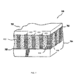
- FIG. 7 shows an illustration of a sensor array according to an embodiment of the present invention.
- FIG. 8 shows a flowchart showing example steps for manufacturing a net-shaped sintered ceramic body according to an embodiment of the present invention.
- FIG. 9A shows an illustration of an array with uniform circular micron-sized ceramic elements in a net-shaped ceramic body.
- FIG. 9B shows an illustration of an array with uniform rectangular micron-sized ceramic elements in a net-shaped ceramic body.
- FIG. 9C shows an illustration of an array with various sized circular micron-sized ceramic elements in a net-shaped ceramic body.
- Slip mixture is used herein to refer to the composition comprising the ceramic powder that can be molded to form a molded slip mixture.
- Green body is used herein to mean the molded article that results from molding and setting the slip mixture.
- Cut green body is used herein to refer to the product of cutting/dicing a green body to form an array of a plurality of ceramic elements.
- sintered ceramic body is used herein to refer to the product of sintering a green body.
- the present invention relates to a method of manufacturing a ceramic body, comprising the steps of mixing a ceramic powder, polymer binder, and surfactant to form a slip mixture; casting the slip into a mold and setting to form a ceramic green body; separating the green body from the mold; cutting (dicing) the green body to form an array of micron-sized ceramic elements (pillars) and micron-sized gaps/separations between the elements; and sintering the cut green body to form a sintered ceramic body.
- FIG. 1 is an illustration of a flowchart 100 showing example steps for producing a sintered ceramic body.
- a ceramic powder, polymer binder, a surfactant and optionally dispersant are mixed to form a slip mixture.
- the ceramic powder can be optionally milled (ground with a grinding medium) prior to forming the slip to have a preferred particular particle size and/or size distribution.
- step 104 the slip mixture is cast into a mold and set, step 106 , in the mold to form a green body.
- step 108 the green body is separated (i.e., removed) from the mold so it can be cut or diced to form an array of micron-sized ceramic element with micron-sized separations (kerfs) between the elements in step 110 .
- step 112 the cut green body is heated (sintered) to burn out the binder and densify the body to form a sintered ceramic body.
- the sintered ceramic body can be further processed to form a piezoelectric composite by encasing the sintered ceramic body in a polymer material.
- the piezoelectric composite can be processed to form a device such as a transducer or sensor.
- FIG. 2 is an illustration of a diagram 200 , of slip mixture 202 .
- Slip mixture 202 comprises ceramic powder 204 , polymer binder 206 , surfactant 208 , and optionally dispersant 210 .
- the ceramic powder for use in the present invention can be any piezoelectric or electrostrictive ceramic powder. Such materials are well known in the art and are commercially available. Specific examples include but are not limited to barium titanate, lead titanate, lead zirconate, lead zirconate titanate (PZT), lead niobium titanate (PNT), lead scandium niobium titanate, and any other suitable piezoelectric or electrostrictive ceramic powder known to one skilled in the art.
- a preferred material for use in the present invention is PZT.
- the commercially available ceramic powder can optionally be further processed to a desired form, such as that form having a defined particle size and/or size distribution.
- Controlling the particle size and size distribution is important for controlling shrinkage of the sintered ceramic body. Grinding the ceramic powder to a desired particle size and size distribution improves shrinkage control to avoid cracking of the ceramic body and also allows for increasing the density of the green body by having a high solids loading in slip mixture 202 . Increasing the density of the green body provides improved mechanical strength for dicing and leads to a reduction in the amount of shrinkage during setting and sintering.
- the ceramic powder will have a particle size ranging from 0.2 ⁇ m to 1.6 ⁇ m.
- example particle size distributions are shown in Table 1:
- the ceramic powder can be ground or sheared into its desired particle size/size distribution neat, or alternatively as a mixture comprising the ceramic powder and other materials.
- the ceramic powder can be ground with a grinding medium to produce the desired particle size and/or size distribution. Contamination of the ceramic powder should be prevented.
- a preferred grinding media to prevent contamination is zirconia or beta zirconia.
- Other suitable grinding media include alumina, stainless steel, or any other suitable grinding media that would limit contamination of the ceramic powder to less than 0.02% impurities.
- ceramic powder 204 is ground for 5 hours with a zirconia grinding medium to obtain the preferred particle size and preferred particle size distribution.
- the amount of ceramic powder in slip mixture 202 can vary depending on the desired final properties of the slip mixture, the green body, and the sintered ceramic body. Increasing the amount of ceramic powder in the slip reduces the sinter shrinkage and may increase the density of the resulting sintered ceramic body. More dense bodies have better physical and mechanical properties, such as mechanical strength. However, the processability of the slip is adversely affected as the volume and/or weight fraction of ceramic powder increases. Specifically, the slip becomes more powdery and less pourable.
- Slip mixtures of the present invention comprise a high volume percent (vol. %) and or weight percent (wt. %) of ceramic powder, resulting in dense ceramic bodies, without using excess liquids or solvents to render the slip pourable.
- the high solids loading of ceramic powder 204 in slip mixture 202 reduces shrinkage and increases the density so a green body can be obtained that is substantially the same size and shape as the mold (i.e. there is negligible shrinkage during the setting step).
- the slip 202 has a high solids loading such that slip mixture 202 can comprise about 85-98 wt. % ceramic powder.
- the slip comprises about 90 wt. % ceramic powder.
- slip mixture 202 comprises about 98 vol. % ceramic powder.
- Slip mixture 202 of the present invention comprises low wt. % of polymer binder.
- the slip can comprise 1-10 wt % polymer binder.
- the slip comprises about 9.8 wt % polymer binder, surfactant, and optional dispersant.
- Polymers for use in the present invention include any polymers that bind the ceramic powders and form slip mixtures having viscosities low enough to be flowable, pourable, or injectable.
- the polymers will have a viscosity under 400 cPs at 25° C.
- the term “polymer” includes polymer precursors, pre-polymers, and uncrosslinked polymers mixed with cross-linking agents.
- the polymer is a thermosetting polymer.
- Particular examples of polymers include, but are not limited to, polyesters, polyurethanes, silicone rubbers and epoxy polymers.
- a preferred polymer is low viscosity epoxy polymer resin.
- an epoxy polymer resin provides sufficient mechanical strength so that the green body may be cut/diced without destruction.
- epoxy polymers are not as easily burned out. Controlling temperature during binder burn out is critical to removing all the binder while not causing distortion or cracking of the green body.
- a slow bisquing treatment over a two to three day period is used to more easily remove the epoxy polymer resin.
- epoxy polymer is used herein to refer to uncured epoxy precursors, mixed epoxy precursors and the finished, cured or cross-linked epoxy polymer.
- epoxy polymers suitable for use in the present invention include, but are not limited to, two-part epoxy precursors, three-part epoxy precursors, or epoxy precursors having more than three parts.
- One example of a two part epoxy precursor includes, but is not limited to, a precursor having two or more amine functional groups and another part having two or more epoxide functional groups.
- Epoxy resins are well known to one of ordinary skill in the art. Specific examples of epoxy polymers include D.E.R.
- a two-part epoxy resin is used as binder 206 . Because of the limited shelf life of the epoxy resin, the two parts are mixed for 5 minutes at a temperature of 25° C. to 40° C. only 30 minutes to 2 hours before preparing slip mixture 202 .
- the cure or set time for a thermosetting polymer used is long enough to allow mixing of the slip mixture and casting into the mold before the thermosetting polymer hardens.
- the set time is about 10 minutes to about 48 hours, preferably about 1 hour to about 3 hours.
- surfactants and dispersants are used to control the stability, wettability, flowability, viscosity and other properties of the slip mixture.
- Any surfactant that is compatible with organic polymers can be used.
- the surfactant lowers the surface tension of the polymer and is capable of stabilizing the slip mixture and/or facilitating the formation and molding of the slip mixture.
- surfactants for use in the present invention include, but are not limited to, Dow Corning 57 surfactant, FluoradTM FC-4430 surfactant, FluoradTM FC-4432 surfactant, Surfonic PE-1198 surfactant and KEN-REACT® KR-55 surfactant.
- any dispersant capable of facilitating the dispersion of the ceramic powder into the slip mixture and/or facilitating the formation and molding of the slip mixture can be used in the present invention.
- Specific examples of dispersants suitable for use in the present invention include, but are not limited to, DYSPERBYK® 110 dispersant and Dequest 2010 dispersant.
- slip mixture 202 of the present invention Upon formation, slip mixture 202 of the present invention comprises high vol. % and/or wt. % of ceramic powder, and preferably, comprises no excess liquid and no solvent. Slip mixtures of the present invention are pourable and flowable, having viscosities low enough for slip casting. Slip mixture 202 should have a viscosity of 2000 cPs to 3000 cPs. Because the slip mixtures comprise little to no excess solvent or liquid that requires evaporation to harden the slip, slip mixtures of the present invention have little to substantially no shrinkage upon setting in the mold.
- slip mixture 202 is prepared by combining ceramic powder 204 , binder 206 , surfactant 208 and optional dispersant 210 and mixing using any method known to one of ordinary skill in the relevant art.
- slip mixture 202 can be mixed using a milling mixer, shaker mixer, shear mixer, kinetic shear mixer. The mixture is optionally held under a vacuum during mixing to remove any trapped gases in the slip mixture.
- the slip mixture can be inserted into and mixed in a kinetic shear mixer under vacuum. The mixture is mixed for a time sufficient to produce a fully mixed slip mixture with little to no agglomeration, and the mixing is stopped before the mixture sets and the polymer binder hardens.
- the slip mixture is mixed under vacuum for a time of about 5 minutes to 1 hour at 400 rpm at room temperature.
- the slip mixture is degassed prior to casting into a mold.
- the slip mixture is degassed in a vacuum chamber for 10 minutes at 5 ⁇ 10 ⁇ 1 torr.
- slip mixture 202 is cast into a mold. Any method known to one of ordinary skill in the art can be used to transfer the slip into the mold such as slip casting and injection molding, or any other suitable technique for forming a ceramic body.
- the mold can be of any suitable geometric shape.
- the mold may be circular, square, or any other suitable geometry for a ceramic body for a piezoelectric composite.
- the mold is circular in shape with a diameter range from about 2′′ to about 4′′ and is of sufficient depth to form a green body with a thickness of about 2.5 mm to 3 mm.
- the mold may be square to form green bodies having dimensions of 0.25 inches to 12 inches in both width and length.
- slip mixture 202 is set (cured) in the mold to form a green body.
- the slip in the mold can be optionally degassed before setting/curing to form the green body.
- Slip 202 in the mold is degassed to reduce/avoid air pockets (voids) in the green body.
- the slip and mold can be in a vacuum chamber at 1.2 ⁇ 10 ⁇ 1 torr for a time ranging from 30 minutes to one hour.
- the slip should be set/cured for a sufficient time at a sufficient temperature so that the slip forms a green body 300 that is firm enough to separate from the mold but not brittle, as seen in FIGS. 3A and 3B .
- the green body 300 should have enough mechanical strength to be cut (diced) without fracturing green body 300 .
- the slip is set in the mold by curing for approximately 24 hours in an oven at 120° C.
- the green body is cut (or diced) to form a cut green body with an array of a plurality of micron-sized ceramic elements (pillars) with micron-sized gaps/separations between the elements.
- the green body can optionally be ground to a uniform thickness before dicing.
- the green body can be cut/diced using any suitable dicing method known to one of ordinary skill in the art.
- the green body can be diced using a conventional dicing machine in conventional orientations.
- green body 300 is diced by a dicing machine with a wafer saw.
- the green body can be diced at a rate 25 times to 50 times faster than conventional dicing of a sintered ceramic body.
- the sintered ceramic body can be diced at a rate of 3 ⁇ m/sec to 5 ⁇ m/sec.
- the green body can be diced at a rate of 150 ⁇ m/sec to 300 ⁇ m/sec. This faster rate substantially reduces the time and cost for manufacturing a ceramic body for a piezoelectric composite for a device, for example a transducer or sensor.
- a transducer or sensor produced in accordance with the present invention costs about 2.2 cents per ceramic element/pillar to produce in comparison to a cost of 25 cents per ceramic pillar for traditional dicing methods. Additionally, dicing a green body is not as destructive to the blades of the dicing machine and prolongs the lifetime use of the blades.
- the green body is cut (diced) to form cut green body 400 with an array comprising a plurality of ceramic elements (pillars) 402 separated by kerf (pillar-to-pillar separation) 404 supported by base 406 .
- ceramic elements 402 can range in size from 150 ⁇ m to 325 ⁇ m in height, from 35 ⁇ m to 65 ⁇ m in width, with kerf 402 of less than 25 ⁇ m.
- ceramic elements 402 have a height of 250 ⁇ m, width of 60 ⁇ m, and kerf 404 of 20 ⁇ m.
- step 112 diced green body 400 is sintered to form a sintered ceramic body.
- the sintered ceramic body can be further processed efficiently and effectively.
- spatial temperature gradients present during sintering can cause non-uniform shrinkage such that the kerf size varies across the ceramic body.
- warpage can occur such that the ends of cut green body 400 curl during sintering so that its base 406 is no longer a flat surface. Controlling the temperature distribution during heat-up and cool-down phases is crucial to controlling shrinkage and warpage. Also, having a high solids loading in the slip mixture aids in controlling shrinkage.
- diced green body 400 undergoes a separate bisquing treatment to remove (burn out) the polymer binder before sintering.
- Diced green body 400 is heated in a kiln at sufficient temperature for a sufficient time to burn out the polymer binder. Controlling the temperature during the bisquing treatment is critical to burning out all of the polymers in the green body while preventing the green body from cracking.
- the diced green body is heated to a temperature ranging from 300° C. to 750° C.
- Diced green body 400 undergoes a slow bisquing treatment over a 64 hour period up to a maximum temperature of 750° C. before cooling down.
- Diced green body 400 soaks (held at) 750° C. for 2 hours before cooling down. The slow bisque allows for removing the binder without deforming/distorting the diced ceramic body.
- the ceramic body is further heated (sintered) to form a densified sintered ceramic body.
- the binder removed body is sintered at a sufficient temperature for a sufficient time to densify the body to 97-99% of theoretical density.
- the body is heated at a temperature of about 750° C. to 1100° C.
- the ceramic body is heated over 48 hours up to a maximum temperature of 1060° C. and soaked (held at) the maximum temperature for 1.5 hours.
- the ceramic body is elevated on a support plate with a similar coefficient of expansion to control shrinkage and placed in a kiln to achieve a more uniform temperature gradient above and below the ceramic body. Elevating the ceramic body allows for air flow above and below the ceramic body.
- the ceramic body can be placed on a PZT plate and then into the kiln to undergo sintering step 112 .
- the ceramic body and PZT support plate can be placed in an aluminum crucible and placed in a kiln.
- the aluminum crucible can, optionally, also contain PZT powder.
- the PZT powder is used to control lead loss, which is paramount for achieving constant ceramic material properties throughout the ceramic body. By placing the ceramic body in an equilibrium lead atmosphere lead loss is reduced/avoid.
- FIG. 5 is an illustration of flowchart 500 showing example steps for further processing the sintered ceramic body to fabricate a piezoelectric composite and devices therefrom.
- the sintered ceramic body can be encased/encapsulated in a polymer to form a composite, as indicated in step 502 .
- kerfs 604 the pillar to pillar separations
- a polymer filler 608 to suppress any shear waves and give composite 600 improved mechanical characteristics.
- a polymer filler that provides high acoustical attenuation and electrical isolation should be used or any other suitable polymer filler material known to one skilled in the art.
- piezoelectric composite 600 can be further processed.
- step 504 piezoelectric composite 600 is machined to expose at least one surface of the sintered ceramic body in the composite.
- contacts are formed to the composite to provide electrical connectivity to the sinter ceramic pillars.
- step 508 the sintered ceramic is addressed with electrical components to form a device.
- the micron-sized ceramic elements can be metallized and addressed to form a device, such as an acoustic transducer or sensor for obtaining biometric data and other types of information, such as medical information.
- the device is then polled by applying appropriate voltage at an appropriate temperature for an appropriate time.
- the parameter values vary due to the type of ceramic material used and thickness of the piezoelectric composite being processed.
- FIG. 7 illustrates a device 700 fabricated in accordance with an embodiment of the present invention.
- Device 700 is a multilayer structure that includes a two dimensional array of ceramic pillars 602 .
- Conductors 706 and 708 are connected to each of ceramic pillars 602 .
- Conductors 706 connected to one end of each ceramic pillars 602 are oriented orthogonally with respect to conductors 708 connected to the another end of pillars 602 .
- a shield layer 702 can be added to one side of device 700 to provide a protective coating where a finger can be placed proximate to device 700 .
- a support 704 can be attached to the opposite end of device 700 .
- slip mixture 202 can be injected into a precision mold to form a net-shaped green body with an array comprising a plurality of micron-sized ceramic elements and separations to eliminate the need for dicing the green body.
- FIG. 8 is an illustration of a flowchart 800 showing example steps for producing a net-shaped green body.
- Net-shaped is used herein to mean that green bodies of the present invention have high-quality, micron-sized ceramic elements upon setting in the mold, and no additional machining or processing is required to achieve high quality micron-sized ceramic elements.
- slip mixture 202 can be molded to a net-shaped green body.
- substantially no distortion is used herein to mean flat surfaces of the molded slip mixture remain flat upon setting/curing to form the green body, and the surfaces of the green body are smooth and essentially free of defects larger than about the grain size of the ceramic powder. Defects include, but are not limited to, holes, bubbles, cracks and the like.
- the slip mixtures therefore, can be molded to net-shaped green bodies having high quality micron-sized ceramic elements, and the green bodies can have overall large dimensions.
- the net-shaped green bodies can be made in a wide range of geometries.
- the micron-sized ceramic elements of the net-shaped green body can be uniform in size or vary in size and can be uniform in shape or vary in shape.
- the micron-sized ceramic elements of the net-shaped green body can be circular, square and rectangular in shape.
- the net-shaped green bodies can also comprise micron-sized ceramic elements of one or more dimensional sizes.
- FIGS. 9A , 9 B, and 9 C illustrate some examples of the micron-sized ceramic elements geometries and arrangements that can be produced in accordance with an embodiment of the present invention.
- slip mixture 202 is injected into a mold and set in step 806 to form a net-shaped green body with an array comprising a plurality of micron-sized ceramic elements and separations.
- Slip mixture 202 can be injected into a mold using any method known to one of ordinary skill in the art for injecting or transferring the slip mixture into a mold.
- slip mixture 202 can be injected into a mold using pressure.
- Pressures for use in step 804 include any pressure capable of injecting the slip mixture into the mold. In one embodiment, a pressure of about 5 p.s.i. to 100 p.s.i. at a temperature of about 20° C. to 40° C. is used.
- slip 202 is injected into a mold at a pressure ranging from 60 p.s.i. to 70 p.s.i.
- the molds used for molding the slip mixture and setting to form a net-shaped green body can be any mold capable of forming and releasing micron-sized structural elements without damage.
- materials for use as molds include, but are not limited to, plastics and rubbers. Specific examples of materials include, but are not limited to, low durometer (hardness of less than about 40 A) theromset polyurethanes and silicones.
- the mold is made from a Room Temperature Vulcanization (RTV) silicone.
- slip mixture 202 is set in the mold to form a net-shaped green body with an array comprising a plurality of micron-sized ceramic elements and separations for a sufficient time at a sufficient temperature to be able to separate the green body from the mold without causing damage to the micron-sized ceramic elements. Any method known to one of ordinary skill in the art can be used to set the slip mixture. In a preferred embodiment, slip mixture 202 sets/cures in the mold at room temperature for a period ranging from 18 hours to 36 hours.
- the net-shaped green body is separated from the mold.
- Any method of separating known to one of ordinary skill in the art can be used to separate the net-shaped green body from the mold. Examples of methods include, but are not limited to, peeling or lifting the mold off the green bodies. Preferably, the separation is done so that few or none of the micron-sized ceramic elements are damaged during separation.
- a mold release or release agent can be used to aid in separating the net-shaped green body from the mold without damage. The mold release or release agent can be applied directly to the mold prior to injecting slip mixture 202 into the mold.
- the net-shaped green body After separating the net-shaped green body from the mold, it may undergo a similar bisquing treatment to remove (burn out) the polymer binder before sintering as described above.
- the net-shaped green body can be similarly sintered to form a densified sintered net-shaped ceramic body.
- the resulting sintered net-shaped ceramic body can be further processed as illustrated in FIG. 5 and described above to fabricate a piezoelectric composite and devices therefrom.
Landscapes
- Engineering & Computer Science (AREA)
- Chemical & Material Sciences (AREA)
- Manufacturing & Machinery (AREA)
- Ceramic Engineering (AREA)
- Inorganic Chemistry (AREA)
- Composite Materials (AREA)
- Materials Engineering (AREA)
- Physics & Mathematics (AREA)
- Acoustics & Sound (AREA)
- Signal Processing (AREA)
- Compositions Of Oxide Ceramics (AREA)
- Transducers For Ultrasonic Waves (AREA)
Priority Applications (2)
| Application Number | Priority Date | Filing Date | Title |
|---|---|---|---|
| US12/819,518 US8703040B2 (en) | 2009-06-19 | 2010-06-21 | Method for manufacturing a piezoelectric ceramic body |
| US14/257,966 US20140339459A1 (en) | 2009-06-19 | 2014-04-21 | Method for manufacturing a piezoelectric ceramic body |
Applications Claiming Priority (2)
| Application Number | Priority Date | Filing Date | Title |
|---|---|---|---|
| US21869009P | 2009-06-19 | 2009-06-19 | |
| US12/819,518 US8703040B2 (en) | 2009-06-19 | 2010-06-21 | Method for manufacturing a piezoelectric ceramic body |
Related Child Applications (1)
| Application Number | Title | Priority Date | Filing Date |
|---|---|---|---|
| US14/257,966 Continuation US20140339459A1 (en) | 2009-06-19 | 2014-04-21 | Method for manufacturing a piezoelectric ceramic body |
Publications (2)
| Publication Number | Publication Date |
|---|---|
| US20110010904A1 US20110010904A1 (en) | 2011-01-20 |
| US8703040B2 true US8703040B2 (en) | 2014-04-22 |
Family
ID=43356673
Family Applications (2)
| Application Number | Title | Priority Date | Filing Date |
|---|---|---|---|
| US12/819,518 Active 2031-08-24 US8703040B2 (en) | 2009-06-19 | 2010-06-21 | Method for manufacturing a piezoelectric ceramic body |
| US14/257,966 Abandoned US20140339459A1 (en) | 2009-06-19 | 2014-04-21 | Method for manufacturing a piezoelectric ceramic body |
Family Applications After (1)
| Application Number | Title | Priority Date | Filing Date |
|---|---|---|---|
| US14/257,966 Abandoned US20140339459A1 (en) | 2009-06-19 | 2014-04-21 | Method for manufacturing a piezoelectric ceramic body |
Country Status (7)
| Country | Link |
|---|---|
| US (2) | US8703040B2 (enExample) |
| EP (1) | EP2443679A4 (enExample) |
| JP (1) | JP2012531036A (enExample) |
| KR (1) | KR20120046177A (enExample) |
| CN (1) | CN102484200B (enExample) |
| CA (1) | CA2765941A1 (enExample) |
| WO (1) | WO2010147675A1 (enExample) |
Cited By (48)
| Publication number | Priority date | Publication date | Assignee | Title |
|---|---|---|---|---|
| US9511994B2 (en) | 2012-11-28 | 2016-12-06 | Invensense, Inc. | Aluminum nitride (AlN) devices with infrared absorption structural layer |
| US9618405B2 (en) | 2014-08-06 | 2017-04-11 | Invensense, Inc. | Piezoelectric acoustic resonator based sensor |
| US9617141B2 (en) | 2012-11-28 | 2017-04-11 | Invensense, Inc. | MEMS device and process for RF and low resistance applications |
| US9928398B2 (en) | 2015-08-17 | 2018-03-27 | Invensense, Inc. | Always-on sensor device for human touch |
| US10071539B2 (en) | 2014-09-30 | 2018-09-11 | Apple Inc. | Co-sintered ceramic for electronic devices |
| US10207387B2 (en) | 2015-03-06 | 2019-02-19 | Apple Inc. | Co-finishing surfaces |
| US10216233B2 (en) | 2015-09-02 | 2019-02-26 | Apple Inc. | Forming features in a ceramic component for an electronic device |
| US10315222B2 (en) | 2016-05-04 | 2019-06-11 | Invensense, Inc. | Two-dimensional array of CMOS control elements |
| US10325915B2 (en) | 2016-05-04 | 2019-06-18 | Invensense, Inc. | Two-dimensional array of CMOS control elements |
| US10335979B2 (en) | 2014-09-30 | 2019-07-02 | Apple Inc. | Machining features in a ceramic component for use in an electronic device |
| US10408797B2 (en) | 2016-05-10 | 2019-09-10 | Invensense, Inc. | Sensing device with a temperature sensor |
| US10441975B2 (en) | 2016-05-10 | 2019-10-15 | Invensense, Inc. | Supplemental sensor modes and systems for ultrasonic transducers |
| US10445547B2 (en) | 2016-05-04 | 2019-10-15 | Invensense, Inc. | Device mountable packaging of ultrasonic transducers |
| US10452887B2 (en) | 2016-05-10 | 2019-10-22 | Invensense, Inc. | Operating a fingerprint sensor comprised of ultrasonic transducers |
| US10474862B2 (en) | 2017-06-01 | 2019-11-12 | Invensense, Inc. | Image generation in an electronic device using ultrasonic transducers |
| US10497747B2 (en) | 2012-11-28 | 2019-12-03 | Invensense, Inc. | Integrated piezoelectric microelectromechanical ultrasound transducer (PMUT) on integrated circuit (IC) for fingerprint sensing |
| US10539539B2 (en) | 2016-05-10 | 2020-01-21 | Invensense, Inc. | Operation of an ultrasonic sensor |
| US10542628B2 (en) | 2017-08-02 | 2020-01-21 | Apple Inc. | Enclosure for an electronic device having a shell and internal chassis |
| US10562070B2 (en) | 2016-05-10 | 2020-02-18 | Invensense, Inc. | Receive operation of an ultrasonic sensor |
| US10571434B2 (en) | 2015-10-20 | 2020-02-25 | Sonavation, Inc. | Acoustic sensing through a barrier |
| US10600403B2 (en) | 2016-05-10 | 2020-03-24 | Invensense, Inc. | Transmit operation of an ultrasonic sensor |
| US10632500B2 (en) | 2016-05-10 | 2020-04-28 | Invensense, Inc. | Ultrasonic transducer with a non-uniform membrane |
| US10643052B2 (en) | 2017-06-28 | 2020-05-05 | Invensense, Inc. | Image generation in an electronic device using ultrasonic transducers |
| US10656255B2 (en) | 2016-05-04 | 2020-05-19 | Invensense, Inc. | Piezoelectric micromachined ultrasonic transducer (PMUT) |
| US10670716B2 (en) | 2016-05-04 | 2020-06-02 | Invensense, Inc. | Operating a two-dimensional array of ultrasonic transducers |
| US10706835B2 (en) | 2016-05-10 | 2020-07-07 | Invensense, Inc. | Transmit beamforming of a two-dimensional array of ultrasonic transducers |
| US10726231B2 (en) | 2012-11-28 | 2020-07-28 | Invensense, Inc. | Integrated piezoelectric microelectromechanical ultrasound transducer (PMUT) on integrated circuit (IC) for fingerprint sensing |
| US10755067B2 (en) | 2018-03-22 | 2020-08-25 | Invensense, Inc. | Operating a fingerprint sensor comprised of ultrasonic transducers |
| US10891461B2 (en) | 2017-05-22 | 2021-01-12 | Invensense, Inc. | Live fingerprint detection utilizing an integrated ultrasound and infrared sensor |
| US10936843B2 (en) | 2018-12-28 | 2021-03-02 | Invensense, Inc. | Segmented image acquisition |
| US10936841B2 (en) | 2017-12-01 | 2021-03-02 | Invensense, Inc. | Darkfield tracking |
| US10984209B2 (en) | 2017-12-01 | 2021-04-20 | Invensense, Inc. | Darkfield modeling |
| US10997388B2 (en) | 2017-12-01 | 2021-05-04 | Invensense, Inc. | Darkfield contamination detection |
| US11151355B2 (en) | 2018-01-24 | 2021-10-19 | Invensense, Inc. | Generation of an estimated fingerprint |
| US11176345B2 (en) | 2019-07-17 | 2021-11-16 | Invensense, Inc. | Ultrasonic fingerprint sensor with a contact layer of non-uniform thickness |
| US11188735B2 (en) | 2019-06-24 | 2021-11-30 | Invensense, Inc. | Fake finger detection using ridge features |
| US11216632B2 (en) | 2019-07-17 | 2022-01-04 | Invensense, Inc. | Ultrasonic fingerprint sensor with a contact layer of non-uniform thickness |
| US11216681B2 (en) | 2019-06-25 | 2022-01-04 | Invensense, Inc. | Fake finger detection based on transient features |
| US11232549B2 (en) | 2019-08-23 | 2022-01-25 | Invensense, Inc. | Adapting a quality threshold for a fingerprint image |
| US11243300B2 (en) | 2020-03-10 | 2022-02-08 | Invensense, Inc. | Operating a fingerprint sensor comprised of ultrasonic transducers and a presence sensor |
| US11328165B2 (en) | 2020-04-24 | 2022-05-10 | Invensense, Inc. | Pressure-based activation of fingerprint spoof detection |
| US11392789B2 (en) | 2019-10-21 | 2022-07-19 | Invensense, Inc. | Fingerprint authentication using a synthetic enrollment image |
| US11460957B2 (en) | 2020-03-09 | 2022-10-04 | Invensense, Inc. | Ultrasonic fingerprint sensor with a contact layer of non-uniform thickness |
| US11673165B2 (en) | 2016-05-10 | 2023-06-13 | Invensense, Inc. | Ultrasonic transducer operable in a surface acoustic wave (SAW) mode |
| US11995909B2 (en) | 2020-07-17 | 2024-05-28 | Tdk Corporation | Multipath reflection correction |
| US12174295B2 (en) | 2020-08-07 | 2024-12-24 | Tdk Corporation | Acoustic multipath correction |
| US12197681B2 (en) | 2021-08-25 | 2025-01-14 | Tdk Corporation | Anchor configurations for an array of ultrasonic transducers |
| US12416807B2 (en) | 2021-08-20 | 2025-09-16 | Tdk Corporation | Retinal projection display system |
Families Citing this family (16)
| Publication number | Priority date | Publication date | Assignee | Title |
|---|---|---|---|---|
| WO2013078206A1 (en) * | 2011-11-21 | 2013-05-30 | Smith & Nephew, Inc. | Methods of designing molds for machining cost reduction |
| KR101608447B1 (ko) * | 2011-12-12 | 2016-04-01 | 가부시키가이샤 무라타 세이사쿠쇼 | 압전 배향 세라믹스 및 그 제조방법 |
| TWI501435B (zh) * | 2012-01-19 | 2015-09-21 | Betacera Inc | 壓電複合材料的製程及壓電發電裝置 |
| US20130342488A1 (en) * | 2012-06-26 | 2013-12-26 | Kent Displays Incorporated | Cholesteric liquid crystal writing tablet erased by a piezoelectric transducer |
| CN103779272B (zh) * | 2013-01-11 | 2017-06-20 | 北京纳米能源与系统研究所 | 晶体管阵列及其制备方法 |
| KR101630606B1 (ko) * | 2014-11-07 | 2016-06-15 | 포항공과대학교 산학협력단 | 전극 삽입형 분말사출성형을 이용한 적층형 압전소자 제조방법 및 그에 의해 제조된 적층형 압전 소자 |
| US20170019731A1 (en) * | 2015-07-14 | 2017-01-19 | Lockheed Martin Corporation | Monolithic ceramic transducers with embedded electrodes |
| KR101850127B1 (ko) * | 2017-03-16 | 2018-04-19 | 주식회사 베프스 | 초음파 지문 센서 제조 방법 |
| CN111065613B (zh) * | 2017-06-30 | 2022-06-21 | 奥卢大学 | 陶瓷复合材料 |
| WO2019027268A1 (ko) * | 2017-08-04 | 2019-02-07 | ㈜포인트엔지니어링 | 압전 소재 기둥 및 그 제조방법 |
| CN109648687B (zh) * | 2018-12-24 | 2020-09-01 | 西安文理学院 | 一种复合生物压电陶瓷成型装置及其成型方法 |
| CN109721371A (zh) * | 2019-02-18 | 2019-05-07 | 武汉理工大学 | 一种压电陶瓷阵列的制备方法 |
| CN110265544A (zh) * | 2019-06-24 | 2019-09-20 | 京东方科技集团股份有限公司 | 压电传感器及制备方法、进行指纹识别的方法及电子设备 |
| CN113707802B (zh) * | 2021-08-27 | 2022-10-21 | 成都汇通西电电子有限公司 | 一种矩阵致动器结构及其制备方法 |
| KR102825062B1 (ko) * | 2021-11-22 | 2025-06-26 | 한국전자통신연구원 | 얽힘 광자쌍 생성 장치 |
| KR102675960B1 (ko) * | 2023-08-01 | 2024-06-17 | 국방과학연구소 | 압전센서 |
Citations (13)
| Publication number | Priority date | Publication date | Assignee | Title |
|---|---|---|---|---|
| US5340510A (en) | 1993-04-05 | 1994-08-23 | Materials Systems Incorporated | Method for making piezoelectric ceramic/polymer composite transducers |
| US5548564A (en) | 1992-10-16 | 1996-08-20 | Duke University | Multi-layer composite ultrasonic transducer arrays |
| US5968290A (en) * | 1997-04-03 | 1999-10-19 | Kabushiki Kaisha Toshiba | Permanent magnet material and bonded magnet |
| US20010050514A1 (en) | 1994-08-18 | 2001-12-13 | Gururaja Turukevere R. | Composite piezoelectric transducer arrays with improved acoustical and electrical impedance |
| US20050156362A1 (en) | 2003-11-29 | 2005-07-21 | Joe Arnold | Piezoelectric device and method of manufacturing same |
| JP2005286444A (ja) | 2004-03-29 | 2005-10-13 | Casio Electronics Co Ltd | 超音波トランスデューサ |
| US7132057B2 (en) * | 2003-10-15 | 2006-11-07 | Piezotech, Llc | Compositions for high power piezoelectric ceramics |
| US20070038111A1 (en) | 2005-08-12 | 2007-02-15 | Scimed Life Systems, Inc. | Micromachined imaging transducer |
| CN101028979A (zh) | 2006-02-27 | 2007-09-05 | 西北工业大学 | 钛酸铋钠—钛酸铋钾无铅压电织构陶瓷及其制备方法 |
| US20090159833A1 (en) * | 2005-04-11 | 2009-06-25 | De Liufu | Compositions for high power piezoelectric ceramics |
| US20100239751A1 (en) * | 2009-03-23 | 2010-09-23 | Sonavation, Inc. | Sea of Pillars |
| US20110003522A1 (en) * | 2009-05-15 | 2011-01-06 | Liang Chen | Bio-based aqueous binder for fiberglass insulation materials and non-woven mats |
| US20110306726A1 (en) * | 2010-06-11 | 2011-12-15 | Bailey Brad C | Rapid cure thermosets from 5- and 6- membered cyclic enamine compounds made from dialdehydes |
Family Cites Families (4)
| Publication number | Priority date | Publication date | Assignee | Title |
|---|---|---|---|---|
| US5818149A (en) * | 1996-03-25 | 1998-10-06 | Rutgers, The State University Of New Jersey | Ceramic composites and methods for producing same |
| US6361735B1 (en) * | 1999-09-01 | 2002-03-26 | General Electric Company | Composite ceramic article and method of making |
| JP3997729B2 (ja) * | 2001-06-15 | 2007-10-24 | ブラザー工業株式会社 | 圧電アクチュエータ及びその圧電アクチュエータを用いたインクジェットヘッド並びにそれらの製造方法 |
| JP4563866B2 (ja) * | 2005-05-17 | 2010-10-13 | 日本特殊陶業株式会社 | セラミック積層体の製造方法 |
-
2010
- 2010-06-21 US US12/819,518 patent/US8703040B2/en active Active
- 2010-06-21 KR KR1020127001356A patent/KR20120046177A/ko not_active Withdrawn
- 2010-06-21 EP EP10789879.3A patent/EP2443679A4/en not_active Withdrawn
- 2010-06-21 CA CA2765941A patent/CA2765941A1/en not_active Abandoned
- 2010-06-21 WO PCT/US2010/001778 patent/WO2010147675A1/en not_active Ceased
- 2010-06-21 JP JP2012516070A patent/JP2012531036A/ja active Pending
- 2010-06-21 CN CN201080032563.9A patent/CN102484200B/zh not_active Expired - Fee Related
-
2014
- 2014-04-21 US US14/257,966 patent/US20140339459A1/en not_active Abandoned
Patent Citations (16)
| Publication number | Priority date | Publication date | Assignee | Title |
|---|---|---|---|---|
| US5548564A (en) | 1992-10-16 | 1996-08-20 | Duke University | Multi-layer composite ultrasonic transducer arrays |
| US5340510A (en) | 1993-04-05 | 1994-08-23 | Materials Systems Incorporated | Method for making piezoelectric ceramic/polymer composite transducers |
| US20010050514A1 (en) | 1994-08-18 | 2001-12-13 | Gururaja Turukevere R. | Composite piezoelectric transducer arrays with improved acoustical and electrical impedance |
| US5968290A (en) * | 1997-04-03 | 1999-10-19 | Kabushiki Kaisha Toshiba | Permanent magnet material and bonded magnet |
| US7132057B2 (en) * | 2003-10-15 | 2006-11-07 | Piezotech, Llc | Compositions for high power piezoelectric ceramics |
| US20070181846A1 (en) * | 2003-10-15 | 2007-08-09 | De Liufu | Compositions for high power piezoelectric ceramics |
| US20050156362A1 (en) | 2003-11-29 | 2005-07-21 | Joe Arnold | Piezoelectric device and method of manufacturing same |
| US20050203231A1 (en) | 2003-11-29 | 2005-09-15 | Cross Match Technologies, Inc. | Polymer ceramic slip and method of manufacturing ceramic green bodies there therefrom |
| JP2005286444A (ja) | 2004-03-29 | 2005-10-13 | Casio Electronics Co Ltd | 超音波トランスデューサ |
| US20090159833A1 (en) * | 2005-04-11 | 2009-06-25 | De Liufu | Compositions for high power piezoelectric ceramics |
| US20110204277A1 (en) * | 2005-04-11 | 2011-08-25 | De Liufu | Compositions for high power piezoelectric ceramics |
| US20070038111A1 (en) | 2005-08-12 | 2007-02-15 | Scimed Life Systems, Inc. | Micromachined imaging transducer |
| CN101028979A (zh) | 2006-02-27 | 2007-09-05 | 西北工业大学 | 钛酸铋钠—钛酸铋钾无铅压电织构陶瓷及其制备方法 |
| US20100239751A1 (en) * | 2009-03-23 | 2010-09-23 | Sonavation, Inc. | Sea of Pillars |
| US20110003522A1 (en) * | 2009-05-15 | 2011-01-06 | Liang Chen | Bio-based aqueous binder for fiberglass insulation materials and non-woven mats |
| US20110306726A1 (en) * | 2010-06-11 | 2011-12-15 | Bailey Brad C | Rapid cure thermosets from 5- and 6- membered cyclic enamine compounds made from dialdehydes |
Non-Patent Citations (4)
| Title |
|---|
| European Patent Office, Application No. 10789879.3, Extended European Search Report dated Sep. 6, 2013. |
| International Search Report for International Application No. PCT/US 10/01778, United States Patent and Trademark Office, U.S.A., mailed on Sep. 15, 2010. |
| State Intellectual Property Office of the People's Republic of China, Application No. 201080032563.9, Notification of the First Office Action dated Oct. 10, 2013. |
| The Written Opinion of the International Searching Authority for International Application No. PCT/US 10/01778, United States Patent and Trademark Office, U.S.A., mailed on Sep. 15, 2010. |
Cited By (64)
| Publication number | Priority date | Publication date | Assignee | Title |
|---|---|---|---|---|
| US10726231B2 (en) | 2012-11-28 | 2020-07-28 | Invensense, Inc. | Integrated piezoelectric microelectromechanical ultrasound transducer (PMUT) on integrated circuit (IC) for fingerprint sensing |
| US9511994B2 (en) | 2012-11-28 | 2016-12-06 | Invensense, Inc. | Aluminum nitride (AlN) devices with infrared absorption structural layer |
| US9617141B2 (en) | 2012-11-28 | 2017-04-11 | Invensense, Inc. | MEMS device and process for RF and low resistance applications |
| US10497747B2 (en) | 2012-11-28 | 2019-12-03 | Invensense, Inc. | Integrated piezoelectric microelectromechanical ultrasound transducer (PMUT) on integrated circuit (IC) for fingerprint sensing |
| US10508022B2 (en) | 2012-11-28 | 2019-12-17 | Invensense, Inc. | MEMS device and process for RF and low resistance applications |
| US10160635B2 (en) | 2012-11-28 | 2018-12-25 | Invensense, Inc. | MEMS device and process for RF and low resistance applications |
| US11847851B2 (en) | 2012-11-28 | 2023-12-19 | Invensense, Inc. | Integrated piezoelectric microelectromechanical ultrasound transducer (PMUT) on integrated circuit (IC) for fingerprint sensing |
| US11263424B2 (en) | 2012-11-28 | 2022-03-01 | Invensense, Inc. | Integrated piezoelectric microelectromechanical ultrasound transducer (PMUT) on integrated circuit (IC) for fingerprint sensing |
| US10294097B2 (en) | 2012-11-28 | 2019-05-21 | Invensense, Inc. | Aluminum nitride (AlN) devices with infrared absorption structural layer |
| US9618405B2 (en) | 2014-08-06 | 2017-04-11 | Invensense, Inc. | Piezoelectric acoustic resonator based sensor |
| US10335979B2 (en) | 2014-09-30 | 2019-07-02 | Apple Inc. | Machining features in a ceramic component for use in an electronic device |
| US10071539B2 (en) | 2014-09-30 | 2018-09-11 | Apple Inc. | Co-sintered ceramic for electronic devices |
| US10207387B2 (en) | 2015-03-06 | 2019-02-19 | Apple Inc. | Co-finishing surfaces |
| US9928398B2 (en) | 2015-08-17 | 2018-03-27 | Invensense, Inc. | Always-on sensor device for human touch |
| US10216233B2 (en) | 2015-09-02 | 2019-02-26 | Apple Inc. | Forming features in a ceramic component for an electronic device |
| US10571434B2 (en) | 2015-10-20 | 2020-02-25 | Sonavation, Inc. | Acoustic sensing through a barrier |
| US10315222B2 (en) | 2016-05-04 | 2019-06-11 | Invensense, Inc. | Two-dimensional array of CMOS control elements |
| US11651611B2 (en) | 2016-05-04 | 2023-05-16 | Invensense, Inc. | Device mountable packaging of ultrasonic transducers |
| US10445547B2 (en) | 2016-05-04 | 2019-10-15 | Invensense, Inc. | Device mountable packaging of ultrasonic transducers |
| US11440052B2 (en) | 2016-05-04 | 2022-09-13 | Invensense, Inc. | Two-dimensional array of CMOS control elements |
| US10325915B2 (en) | 2016-05-04 | 2019-06-18 | Invensense, Inc. | Two-dimensional array of CMOS control elements |
| US10670716B2 (en) | 2016-05-04 | 2020-06-02 | Invensense, Inc. | Operating a two-dimensional array of ultrasonic transducers |
| US10656255B2 (en) | 2016-05-04 | 2020-05-19 | Invensense, Inc. | Piezoelectric micromachined ultrasonic transducer (PMUT) |
| US10441975B2 (en) | 2016-05-10 | 2019-10-15 | Invensense, Inc. | Supplemental sensor modes and systems for ultrasonic transducers |
| US11626099B2 (en) | 2016-05-10 | 2023-04-11 | Invensense, Inc. | Transmit beamforming of a two-dimensional array of ultrasonic transducers |
| US10600403B2 (en) | 2016-05-10 | 2020-03-24 | Invensense, Inc. | Transmit operation of an ultrasonic sensor |
| US10452887B2 (en) | 2016-05-10 | 2019-10-22 | Invensense, Inc. | Operating a fingerprint sensor comprised of ultrasonic transducers |
| US10562070B2 (en) | 2016-05-10 | 2020-02-18 | Invensense, Inc. | Receive operation of an ultrasonic sensor |
| US10706835B2 (en) | 2016-05-10 | 2020-07-07 | Invensense, Inc. | Transmit beamforming of a two-dimensional array of ultrasonic transducers |
| US10408797B2 (en) | 2016-05-10 | 2019-09-10 | Invensense, Inc. | Sensing device with a temperature sensor |
| US10632500B2 (en) | 2016-05-10 | 2020-04-28 | Invensense, Inc. | Ultrasonic transducer with a non-uniform membrane |
| US11673165B2 (en) | 2016-05-10 | 2023-06-13 | Invensense, Inc. | Ultrasonic transducer operable in a surface acoustic wave (SAW) mode |
| US11112388B2 (en) | 2016-05-10 | 2021-09-07 | Invensense, Inc. | Operation of an ultrasonic sensor |
| US11471912B2 (en) | 2016-05-10 | 2022-10-18 | Invensense, Inc. | Supplemental sensor modes and systems for ultrasonic transducers |
| US10539539B2 (en) | 2016-05-10 | 2020-01-21 | Invensense, Inc. | Operation of an ultrasonic sensor |
| US11288891B2 (en) | 2016-05-10 | 2022-03-29 | Invensense, Inc. | Operating a fingerprint sensor comprised of ultrasonic transducers |
| US11154906B2 (en) | 2016-05-10 | 2021-10-26 | Invensense, Inc. | Receive operation of an ultrasonic sensor |
| US10891461B2 (en) | 2017-05-22 | 2021-01-12 | Invensense, Inc. | Live fingerprint detection utilizing an integrated ultrasound and infrared sensor |
| US10860831B2 (en) | 2017-06-01 | 2020-12-08 | Invensense, Inc. | Image generation in an electronic device using ultrasonic transducers |
| US10474862B2 (en) | 2017-06-01 | 2019-11-12 | Invensense, Inc. | Image generation in an electronic device using ultrasonic transducers |
| US10643052B2 (en) | 2017-06-28 | 2020-05-05 | Invensense, Inc. | Image generation in an electronic device using ultrasonic transducers |
| US10542628B2 (en) | 2017-08-02 | 2020-01-21 | Apple Inc. | Enclosure for an electronic device having a shell and internal chassis |
| US10997388B2 (en) | 2017-12-01 | 2021-05-04 | Invensense, Inc. | Darkfield contamination detection |
| US10936841B2 (en) | 2017-12-01 | 2021-03-02 | Invensense, Inc. | Darkfield tracking |
| US10984209B2 (en) | 2017-12-01 | 2021-04-20 | Invensense, Inc. | Darkfield modeling |
| US11151355B2 (en) | 2018-01-24 | 2021-10-19 | Invensense, Inc. | Generation of an estimated fingerprint |
| US12002282B2 (en) | 2018-03-22 | 2024-06-04 | Invensense, Inc. | Operating a fingerprint sensor comprised of ultrasonic transducers |
| US10755067B2 (en) | 2018-03-22 | 2020-08-25 | Invensense, Inc. | Operating a fingerprint sensor comprised of ultrasonic transducers |
| US10936843B2 (en) | 2018-12-28 | 2021-03-02 | Invensense, Inc. | Segmented image acquisition |
| US11188735B2 (en) | 2019-06-24 | 2021-11-30 | Invensense, Inc. | Fake finger detection using ridge features |
| US11216681B2 (en) | 2019-06-25 | 2022-01-04 | Invensense, Inc. | Fake finger detection based on transient features |
| US11216632B2 (en) | 2019-07-17 | 2022-01-04 | Invensense, Inc. | Ultrasonic fingerprint sensor with a contact layer of non-uniform thickness |
| US11682228B2 (en) | 2019-07-17 | 2023-06-20 | Invensense, Inc. | Ultrasonic fingerprint sensor with a contact layer of non-uniform thickness |
| US11176345B2 (en) | 2019-07-17 | 2021-11-16 | Invensense, Inc. | Ultrasonic fingerprint sensor with a contact layer of non-uniform thickness |
| US11232549B2 (en) | 2019-08-23 | 2022-01-25 | Invensense, Inc. | Adapting a quality threshold for a fingerprint image |
| US11392789B2 (en) | 2019-10-21 | 2022-07-19 | Invensense, Inc. | Fingerprint authentication using a synthetic enrollment image |
| US11460957B2 (en) | 2020-03-09 | 2022-10-04 | Invensense, Inc. | Ultrasonic fingerprint sensor with a contact layer of non-uniform thickness |
| US11243300B2 (en) | 2020-03-10 | 2022-02-08 | Invensense, Inc. | Operating a fingerprint sensor comprised of ultrasonic transducers and a presence sensor |
| US11328165B2 (en) | 2020-04-24 | 2022-05-10 | Invensense, Inc. | Pressure-based activation of fingerprint spoof detection |
| US11995909B2 (en) | 2020-07-17 | 2024-05-28 | Tdk Corporation | Multipath reflection correction |
| US12174295B2 (en) | 2020-08-07 | 2024-12-24 | Tdk Corporation | Acoustic multipath correction |
| US12416807B2 (en) | 2021-08-20 | 2025-09-16 | Tdk Corporation | Retinal projection display system |
| US12197681B2 (en) | 2021-08-25 | 2025-01-14 | Tdk Corporation | Anchor configurations for an array of ultrasonic transducers |
| US12260050B2 (en) | 2021-08-25 | 2025-03-25 | Tdk Corporation | Differential receive at an ultrasonic transducer |
Also Published As
| Publication number | Publication date |
|---|---|
| US20140339459A1 (en) | 2014-11-20 |
| US20110010904A1 (en) | 2011-01-20 |
| CA2765941A1 (en) | 2010-12-23 |
| CN102484200A (zh) | 2012-05-30 |
| EP2443679A4 (en) | 2013-10-09 |
| KR20120046177A (ko) | 2012-05-09 |
| EP2443679A1 (en) | 2012-04-25 |
| CN102484200B (zh) | 2015-11-25 |
| JP2012531036A (ja) | 2012-12-06 |
| WO2010147675A1 (en) | 2010-12-23 |
Similar Documents
| Publication | Publication Date | Title |
|---|---|---|
| US8703040B2 (en) | Method for manufacturing a piezoelectric ceramic body | |
| US5340510A (en) | Method for making piezoelectric ceramic/polymer composite transducers | |
| US20050203231A1 (en) | Polymer ceramic slip and method of manufacturing ceramic green bodies there therefrom | |
| EP1227525B1 (en) | Piezocomposite, ultrasonic probe for ultrasonic diagnostic equipment, ultrasonic diagnostic equipment and method for producing piezocomposite | |
| JP2012531036A5 (enExample) | ||
| JPH04232425A (ja) | 複合超音波変換器 | |
| KR101041199B1 (ko) | 세라믹 성형체, 세라믹 부품, 세라믹 성형체의 제조 방법및 세라믹 부품의 제조 방법 | |
| KR101620296B1 (ko) | 적층형 압전 세라믹 소자 | |
| CN113710444B (zh) | 三维烧成体的制法 | |
| JP6676835B1 (ja) | ウエハ載置台の製法 | |
| JP5275946B2 (ja) | セラミック成形体の製造方法 | |
| US6228318B1 (en) | Manufacturing method of ceramics component having microstructure | |
| KR101630826B1 (ko) | 전자세라믹 소성용 고강도 세라믹 기판의 제조방법 및 이에 의해 제조되는 전자세라믹 소성용 고강도 세라믹 기판 | |
| US11746062B2 (en) | Processes for preparing porous ceramics for acoustic transducers | |
| JP5103346B2 (ja) | セラミック成形体の製造方法、及びセラミック部材の製造方法 | |
| JP7216611B2 (ja) | SiC焼結部材の製造方法 | |
| KR20230088153A (ko) | 압전소재 제조방법 및 이를 이용하여 제조된 압전소자 | |
| Bandyopadhyay et al. | Processing of Piezocomposites via Solid Freeform Fabrication (SFF) Techniques | |
| KR101243745B1 (ko) | 세라믹 부재 및 세라믹 부재의 제조 방법 | |
| Kiggans Jr et al. | Gelcast Forming of PZT Materials | |
| Bandyopadhyay et al. | Processing of Piezocomposites via Solid Freeform Fabrication (SFF) | |
| Hoffmann et al. | Open Ceramics | |
| JPH08225370A (ja) | 圧電セラミックスの製造方法 |
Legal Events
| Date | Code | Title | Description |
|---|---|---|---|
| AS | Assignment |
Owner name: CROSS MATCH TECHNOLOGIES, INC., FLORIDA Free format text: ASSIGNMENT OF SECURITY INTEREST;ASSIGNOR:SONAVATION, INC.;REEL/FRAME:025066/0580 Effective date: 20100920 |
|
| AS | Assignment |
Owner name: SONAVATION, INC., FLORIDA Free format text: ASSIGNMENT OF ASSIGNORS INTEREST;ASSIGNORS:LIUFU, DE;REGNIERE, LOUIS;REEL/FRAME:025072/0915 Effective date: 20100908 |
|
| STCF | Information on status: patent grant |
Free format text: PATENTED CASE |
|
| MAFP | Maintenance fee payment |
Free format text: PAYMENT OF MAINTENANCE FEE, 4TH YR, SMALL ENTITY (ORIGINAL EVENT CODE: M2551) Year of fee payment: 4 |
|
| AS | Assignment |
Owner name: CROSS MATCH TECHNOLOGIES, INC., FLORIDA Free format text: SECURITY INTEREST;ASSIGNOR:SONAVATION, INC.;REEL/FRAME:056041/0805 Effective date: 20100917 |
|
| MAFP | Maintenance fee payment |
Free format text: PAYMENT OF MAINTENANCE FEE, 8TH YR, SMALL ENTITY (ORIGINAL EVENT CODE: M2552); ENTITY STATUS OF PATENT OWNER: SMALL ENTITY Year of fee payment: 8 |
|
| AS | Assignment |
Owner name: WEINTZ, KARL F., FLORIDA Free format text: SECURITY INTEREST;ASSIGNOR:SONAVATION, INC.;REEL/FRAME:063271/0954 Effective date: 20220421 Owner name: SONINVEST LLC, DISTRICT OF COLUMBIA Free format text: SECURITY INTEREST;ASSIGNOR:SONAVATION, INC.;REEL/FRAME:063271/0954 Effective date: 20220421 Owner name: BOARD OF REGENTS OF THE UNIVERSITY OF TEXAS SYSTEM ON BEHALF OF THE UNIVERSITY OF TEXAS M.D. ANDERSON CANCER CENTER, TEXAS Free format text: SECURITY INTEREST;ASSIGNOR:SONAVATION, INC.;REEL/FRAME:063271/0954 Effective date: 20220421 Owner name: LOCKE LORD LLP, FLORIDA Free format text: SECURITY INTEREST;ASSIGNOR:SONAVATION, INC.;REEL/FRAME:063271/0954 Effective date: 20220421 Owner name: HEALTHCARE INVESTMENTS, LLC, PUERTO RICO Free format text: SECURITY INTEREST;ASSIGNOR:SONAVATION, INC.;REEL/FRAME:063271/0954 Effective date: 20220421 |
|
| AS | Assignment |
Owner name: BRAZOS CAPITAL MANAGEMENT LLC, TEXAS Free format text: ASSIGNMENT OF ASSIGNORS INTEREST;ASSIGNOR:SONAVATION INC.;REEL/FRAME:068598/0339 Effective date: 20240731 |
|
| AS | Assignment |
Owner name: SONAVATION TECHNOLOGIES, LLC, TEXAS Free format text: ASSIGNMENT OF ASSIGNORS INTEREST;ASSIGNOR:BRAZOS CAPITAL MANAGEMENT LLC;REEL/FRAME:071977/0782 Effective date: 20250808 |
|
| MAFP | Maintenance fee payment |
Free format text: PAYMENT OF MAINTENANCE FEE, 12TH YR, SMALL ENTITY (ORIGINAL EVENT CODE: M2553); ENTITY STATUS OF PATENT OWNER: SMALL ENTITY Year of fee payment: 12 |