US10071539B2 - Co-sintered ceramic for electronic devices - Google Patents
Co-sintered ceramic for electronic devices Download PDFInfo
- Publication number
- US10071539B2 US10071539B2 US14/864,618 US201514864618A US10071539B2 US 10071539 B2 US10071539 B2 US 10071539B2 US 201514864618 A US201514864618 A US 201514864618A US 10071539 B2 US10071539 B2 US 10071539B2
- Authority
- US
- United States
- Prior art keywords
- ceramic
- housing
- parts
- sintering
- ceramic material
- Prior art date
- Legal status (The legal status is an assumption and is not a legal conclusion. Google has not performed a legal analysis and makes no representation as to the accuracy of the status listed.)
- Active, expires
Links
Images


Classifications
-
- B—PERFORMING OPERATIONS; TRANSPORTING
- B32—LAYERED PRODUCTS
- B32B—LAYERED PRODUCTS, i.e. PRODUCTS BUILT-UP OF STRATA OF FLAT OR NON-FLAT, e.g. CELLULAR OR HONEYCOMB, FORM
- B32B18/00—Layered products essentially comprising ceramics, e.g. refractory products
-
- B—PERFORMING OPERATIONS; TRANSPORTING
- B28—WORKING CEMENT, CLAY, OR STONE
- B28B—SHAPING CLAY OR OTHER CERAMIC COMPOSITIONS; SHAPING SLAG; SHAPING MIXTURES CONTAINING CEMENTITIOUS MATERIAL, e.g. PLASTER
- B28B1/00—Producing shaped prefabricated articles from the material
- B28B1/002—Producing shaped prefabricated articles from the material assembled from preformed elements
-
- B—PERFORMING OPERATIONS; TRANSPORTING
- B28—WORKING CEMENT, CLAY, OR STONE
- B28B—SHAPING CLAY OR OTHER CERAMIC COMPOSITIONS; SHAPING SLAG; SHAPING MIXTURES CONTAINING CEMENTITIOUS MATERIAL, e.g. PLASTER
- B28B1/00—Producing shaped prefabricated articles from the material
- B28B1/008—Producing shaped prefabricated articles from the material made from two or more materials having different characteristics or properties
-
- B—PERFORMING OPERATIONS; TRANSPORTING
- B28—WORKING CEMENT, CLAY, OR STONE
- B28B—SHAPING CLAY OR OTHER CERAMIC COMPOSITIONS; SHAPING SLAG; SHAPING MIXTURES CONTAINING CEMENTITIOUS MATERIAL, e.g. PLASTER
- B28B7/00—Moulds; Cores; Mandrels
- B28B7/0088—Moulds in which at least one surface of the moulded article serves as mould surface, e.g. moulding articles on or against a previously shaped article, between previously shaped articles
-
- C—CHEMISTRY; METALLURGY
- C04—CEMENTS; CONCRETE; ARTIFICIAL STONE; CERAMICS; REFRACTORIES
- C04B—LIME, MAGNESIA; SLAG; CEMENTS; COMPOSITIONS THEREOF, e.g. MORTARS, CONCRETE OR LIKE BUILDING MATERIALS; ARTIFICIAL STONE; CERAMICS; REFRACTORIES; TREATMENT OF NATURAL STONE
- C04B35/00—Shaped ceramic products characterised by their composition; Ceramics compositions; Processing powders of inorganic compounds preparatory to the manufacturing of ceramic products
- C04B35/622—Forming processes; Processing powders of inorganic compounds preparatory to the manufacturing of ceramic products
- C04B35/64—Burning or sintering processes
- C04B35/645—Pressure sintering
-
- H—ELECTRICITY
- H04—ELECTRIC COMMUNICATION TECHNIQUE
- H04M—TELEPHONIC COMMUNICATION
- H04M1/00—Substation equipment, e.g. for use by subscribers
- H04M1/02—Constructional features of telephone sets
- H04M1/0202—Portable telephone sets, e.g. cordless phones, mobile phones or bar type handsets
-
- C—CHEMISTRY; METALLURGY
- C04—CEMENTS; CONCRETE; ARTIFICIAL STONE; CERAMICS; REFRACTORIES
- C04B—LIME, MAGNESIA; SLAG; CEMENTS; COMPOSITIONS THEREOF, e.g. MORTARS, CONCRETE OR LIKE BUILDING MATERIALS; ARTIFICIAL STONE; CERAMICS; REFRACTORIES; TREATMENT OF NATURAL STONE
- C04B2235/00—Aspects relating to ceramic starting mixtures or sintered ceramic products
- C04B2235/60—Aspects relating to the preparation, properties or mechanical treatment of green bodies or pre-forms
- C04B2235/602—Making the green bodies or pre-forms by moulding
- C04B2235/6022—Injection moulding
-
- C—CHEMISTRY; METALLURGY
- C04—CEMENTS; CONCRETE; ARTIFICIAL STONE; CERAMICS; REFRACTORIES
- C04B—LIME, MAGNESIA; SLAG; CEMENTS; COMPOSITIONS THEREOF, e.g. MORTARS, CONCRETE OR LIKE BUILDING MATERIALS; ARTIFICIAL STONE; CERAMICS; REFRACTORIES; TREATMENT OF NATURAL STONE
- C04B2235/00—Aspects relating to ceramic starting mixtures or sintered ceramic products
- C04B2235/60—Aspects relating to the preparation, properties or mechanical treatment of green bodies or pre-forms
- C04B2235/602—Making the green bodies or pre-forms by moulding
- C04B2235/6023—Gel casting
-
- C—CHEMISTRY; METALLURGY
- C04—CEMENTS; CONCRETE; ARTIFICIAL STONE; CERAMICS; REFRACTORIES
- C04B—LIME, MAGNESIA; SLAG; CEMENTS; COMPOSITIONS THEREOF, e.g. MORTARS, CONCRETE OR LIKE BUILDING MATERIALS; ARTIFICIAL STONE; CERAMICS; REFRACTORIES; TREATMENT OF NATURAL STONE
- C04B2235/00—Aspects relating to ceramic starting mixtures or sintered ceramic products
- C04B2235/70—Aspects relating to sintered or melt-casted ceramic products
- C04B2235/96—Properties of ceramic products, e.g. mechanical properties such as strength, toughness, wear resistance
- C04B2235/9607—Thermal properties, e.g. thermal expansion coefficient
- C04B2235/9615—Linear firing shrinkage
-
- C—CHEMISTRY; METALLURGY
- C04—CEMENTS; CONCRETE; ARTIFICIAL STONE; CERAMICS; REFRACTORIES
- C04B—LIME, MAGNESIA; SLAG; CEMENTS; COMPOSITIONS THEREOF, e.g. MORTARS, CONCRETE OR LIKE BUILDING MATERIALS; ARTIFICIAL STONE; CERAMICS; REFRACTORIES; TREATMENT OF NATURAL STONE
- C04B2237/00—Aspects relating to ceramic laminates or to joining of ceramic articles with other articles by heating
- C04B2237/30—Composition of layers of ceramic laminates or of ceramic or metallic articles to be joined by heating, e.g. Si substrates
- C04B2237/32—Ceramic
- C04B2237/34—Oxidic
- C04B2237/343—Alumina or aluminates
-
- C—CHEMISTRY; METALLURGY
- C04—CEMENTS; CONCRETE; ARTIFICIAL STONE; CERAMICS; REFRACTORIES
- C04B—LIME, MAGNESIA; SLAG; CEMENTS; COMPOSITIONS THEREOF, e.g. MORTARS, CONCRETE OR LIKE BUILDING MATERIALS; ARTIFICIAL STONE; CERAMICS; REFRACTORIES; TREATMENT OF NATURAL STONE
- C04B2237/00—Aspects relating to ceramic laminates or to joining of ceramic articles with other articles by heating
- C04B2237/30—Composition of layers of ceramic laminates or of ceramic or metallic articles to be joined by heating, e.g. Si substrates
- C04B2237/32—Ceramic
- C04B2237/34—Oxidic
- C04B2237/345—Refractory metal oxides
- C04B2237/348—Zirconia, hafnia, zirconates or hafnates
-
- H—ELECTRICITY
- H04—ELECTRIC COMMUNICATION TECHNIQUE
- H04M—TELEPHONIC COMMUNICATION
- H04M1/00—Substation equipment, e.g. for use by subscribers
- H04M1/02—Constructional features of telephone sets
- H04M1/0202—Portable telephone sets, e.g. cordless phones, mobile phones or bar type handsets
- H04M1/026—Details of the structure or mounting of specific components
- H04M1/0266—Details of the structure or mounting of specific components for a display module assembly
Definitions
- Embodiments disclosed herein relate to ceramic parts for use in portable electronic devices. More particularly, embodiments relate to methods for machining ceramic parts before being completely sintered.
- the relatively light weight of ceramic material in relation to its relatively high degree of hardness and scratch resistance weighs in favor of using ceramic parts for structural and/or protective components. Ceramics may also help the device meet consumer's demands for aesthetically pleasing and refined surface finishes.
- Ceramic parts may be difficult to form with fine or precise features, particularly using traditional machining techniques.
- One embodiment may take the form of a method for manufacturing a ceramic component for a portable electronic device, comprising: forming a first part from a first ceramic material; forming a second part from a second ceramic material; and simultaneously sintering the first part and second part, thereby fusing the first part to the second part to form the ceramic component.
- Another embodiment may take the form of a component for a portable electronic device, comprising: a first part formed from a first ceramic material having a first property; and a second part formed from a second ceramic material having a second property; wherein the first and second parts are fused together during sintering; and the first property is different from the second property.
- Still another embodiment may take the form of a method for forming a co-sintered structure, comprising: molding, using first mold piece and a second mold piece, a first part from a first ceramic slurry; co-molding to the first part, using the first mold piece and a third mold piece, a second part from a second ceramic slurry; and co-sintering the first and second parts, thereby forming the co-sintered structure.
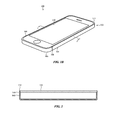
- FIG. 1A depicts a sample electronic device having a housing at least partially formed as a co-sintered ceramic structure
- FIG. 1B depicts the sample electronic device of FIG. 1A , showing a joint within the housing;
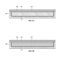
- FIG. 2 is a cross-sectional view of the electronic device taken along line 2 - 2 of FIG. 1B with internal components removed for clarity;
- FIG. 3 is a schematic diagram of a sample system for forming a co-sintered structure
- FIG. 4 is a cross-sectional view of a first part of a co-sintered structure in a mold
- FIG. 5A is a cross-sectional view of a first and second part of a co-sintered structure in a mold:
- FIG. 5B is an alternative cross-sectional view of a first and second part of a co-sintered structure in a mold
- FIG. 6 illustrates another sample co-sintered structure
- FIG. 7 is a flowchart detailing a sample method for creating a co-sintered structure.
- a co-sintered structure may be formed from a first ceramic part and a second ceramic part (or simply, first and second parts).
- the first and second parts may be formed from different ceramic materials and may have different physical and/or chemical properties.
- one part may be transparent while the other is opaque.
- one part may be formed from zirconia and another from alumina.
- one part may be a first color ceramic and a second part may be a second color ceramic.
- the first and second parts may be molded such that they are affixed to and/or abutting one another, and then simultaneously sintered to fuse the parts together.
- boundaries, seams, joints, and other points at which the two ceramics touch may fuse.
- the ceramics of the first and second part may fuse to one another during sintering, thereby ensuring that the co-sintered structure appears (and in many cases, is) a unitary element with no discrete sections.
- grains may migrate between ceramics at their common boundaries. This may create an even stronger bond, interface, and/or surface between the two ceramics (e.g., the first part and second part).
- ceramic components that are co-sintered structures, as described herein, may be strong, unitary, and/or aesthetically pleasing.
- FIGS. 1A-1B depict a sample electronic device 100 , here illustrated as a mobile phone.
- the device 100 may include a housing 102 affixed to a cover surface 110 .
- the housing 102 and cover surface 110 cooperate to form an exterior surface of the electronic device 100 .
- Various components may be housed within the electronic device 100 , such as a display visible through the cover surface 110 .
- the cover surface 110 may be transparent to permit viewing such a display.
- the cover surface 110 and housing 104 may be co-sintered to from a unified structure.
- the two parts may be molded together in a single mold, for example, in a two-step molding process using a common first mold piece, a second mold piece associated with the first part, and a third mold piece associated with the second part.
- the parts may be placed in a sintering furnace and sintered simultaneously, thereby forming a ceramic component that is a co-sintered structure. It should be appreciated that the two parts may be separately molded and joined or placed together in the sintering furnace, and then co-sintered, in some embodiments.
- the housing 104 may be split into a housing 104 and end cap 106 .
- the housing and end cap 104 , 106 may meet at a joint 108 , shown to best effect in FIG. 1B .
- the housing and end cap are attached to one another at the joint 108 .
- the joint may be a mechanical, chemical, other bond between the upper and end cap.
- the joint may be filled such that its surface is flush with the housing 104 and end cap 106 , thereby forming a contiguous, continuous surface between housing and end cap.
- end cap is used herein, it should be appreciated that any structure of any size and/or shape may be an end cap. For example, a flat, planar structure may serve as an end cap.
- the housing may define a lip 112 that extends about a cover surface 110 .
- the lip 112 may be integral with one or both of the upper and end caps 104 , 106 .
- the lip 112 may be relatively flat and flush with the cover surface 110 , or it may be proud or recessed from the cover surface. The lip is shown to better effect in the cross-sectional view of FIG. 2 .
- both the housing 102 and the cover surface 110 may be made of a ceramic, such as zirconia, alumina and the like.
- the cover surface 110 may be formed from a transparent zirconia ceramic and the housing 102 from an opaque zirconia ceramic.
- the cover surface may be colored or tinted (at least in part) while the housing has a different color or tint.
- one of the cover surface 110 and housing 102 may be at least partially formed from black zirconia and one may be formed from white zirconia.
- the cover surface may be alumina and the housing may be zirconia.
- the cover surface may be a polycrystalline alumina.
- FIG. 2 is a cross-sectional view taken along line 2 - 2 of FIG. 1A , omitting internal components of the electronic device 100 for simplicity and clarity.
- the lip 112 defines a step or receiving surface 200 .
- This step receives the cover surface 110 and may act as a support for the cover surface during manufacturing.
- cover surface 110 and housing 104 may be unitary.
- the cover surface 110 and housing 104 (or end cap, in some embodiments) may bond together during manufacturing operations to form a single piece. In many embodiments, this single piece lacks part lines, joints, or any visible separation (other than any difference in material properties) between the two structures.
- the housing 102 and cover surface 110 may be formed in a two-part molding process, followed by a sintering operation that simultaneously sinters both parts in the same sintering furnace.
- the process may cause the two ceramic parts (e.g., housing 104 and cover surface 110 ) to fuse together.
- grains/crystalline structures from one part may effectively dope the other part, and vice versa.
- portions of each ceramic may migrate across a border or abutting surfaces, such that the ceramic intermingle to form a strong chemical bond and a transition region between the two ceramics.
- the transition region may have varying concentrations of each ceramic; typically, the concentration will vary with the amount and/or thickness of each ceramic, the relative amount of each ceramic on either side of the border, and so on.
- a finished (e.g., fully sintered) structure may have crystal formation between the initial two surfaces, thereby effectively joining them as a single piece.
- the finished structure may be referred to as a “co-sintered” structure.
- FIG. 3 illustrates sample machinery for forming a co-sintered structure.
- the machinery may be used to mold multiple parts, typically in such a fashion that they are affixed to one another after molding, and then sinter the parts simultaneously.
- Molding refers to the formation of a solid from a powder, slurry, particulate, or other suitable source. Molding encompasses the use of heat, pressure or both to form the solid. Blow molding, compression molding, and injection molding are all examples of molding.
- First and second parts may be injection molded, for example. In some embodiments, the first and second parts may be molded with a common, first mold piece that is joined with a second mold piece to form the first part, and a third mold piece to form the second part.
- a mold base 300 may be paired with either a first top mold 302 or a second top mold 304 .
- the mold base 300 and first top mold 302 may be used to form a first part ultimately included in a co-sintered structure, such as the housing 102 .
- the first top mold 302 may be removed from the mold base 300 and the second top mold 304 may be placed in, or otherwise paired with, the mold base.
- the mold base 300 and second top mold 304 may cooperate to form a second part ultimately included in the co-sintered structure.
- the mold base may be the first mold piece, the first top mold the second mold piece, and the second top mold the third mold piece.
- a top mold may be the common (e.g., first) mold piece in certain embodiments, while different mold bases are used.
- the second part is formed on or adjacent the first part.
- the first part may remain in the mold base 300 while the second part is formed thereon or adjacent thereto.
- the first part may at least partly support the second part during molding and/or sintering, or may provide a surface on which at least a portion of the second part may be molded or otherwise formed.
- a sintering furnace 306 may be used to sinter the first and second parts to form the co-sintered structure.
- the first and second parts once joined together during the molding operations, may be placed in the sintering furnace; heat and/or pressure may be applied to co-sintered structure.
- the heat and/or pressure compacts the first and second parts, forming them into a single, unified structure. Sintering the co-sintered structure, and the results thereof, are described in more detail below.
- FIGS. 4-5B provide an example of forming a co-sintered structure.
- FIGS. 4-5B illustrate a simplified process for forming the cover surface 110 and housing 104 of FIGS. 1A-1B as a co-sintered structure.
- FIGS. 4-5B are cross-sectional views and are intended for illustration of one sample process and/or structure only, although embodiments and teachings herein may be broadly applied and used to form many different co-sintered structures.
- the first top mold 302 mates to the mold base 300 .
- the first top mold 302 and mold base 300 define a first mold cavity therebetween.
- This cavity may be filled with a ceramic.
- a first ceramic material may be injection molded in the cavity between the mold base 300 and first top mold.
- sufficient heat and/or pressure may be applied to the first ceramic material within the cavity to set, but not fully sinter, it.
- the first ceramic material may be partially sintered, for example to a green state. In other embodiments, the ceramic may be pressed and/or heated to form a part, but not sintered.
- the first ceramic material may form the housing 104 .
- the cover surface 110 may be formed (e.g., molded). Typically, the cover surface 110 is molded on, and is supported in the mold by, the housing 104 . As previously mentioned, the cover surface 110 and housing 104 (or any first and second parts that will be formed into co-sintered structure) may be formed from two different ceramics, thereby permitting different parts of the finished structure to have different physical properties. In the current example, the cover surface 110 may be transparent while the housing 104 is opaque or translucent. In other embodiments, the two parts may have different hardnesses, scratch resistances, indices of refraction, Young's moduli, and so on.
- a mold insert 500 may be placed within the mold base 300 prior to forming the cover surface 110 (or other second part of a co-sintered structure).
- the mold insert 500 may be placed within, upon, or otherwise adjacent the housing 104 (e.g., first part).
- the mold insert 500 may cooperate with the housing 104 to support and form at least part of a second mold cavity for the cover surface 110 during molding.
- the mold insert 500 may be formed from a material that will not chemically react with the ceramics of the housing 104 and cover surface 110 , so that the insert may be removed after the top surface is molded.
- the second top mold 304 may be mated to the mold base 300 .
- the second top mold 304 , mold insert 500 , and housing 104 may cooperate to form the second mold cavity in which the cover surface 110 may be molded.
- the mold base 300 may also form part of this cavity.
- a ceramic slurry, powder, mixture, or the like may be placed, poured or otherwise deposited into the second mold cavity. Heat and/or pressure may be applied to the mold (e.g., the combination of mold base 300 and second top mold 304 ) for a period of time sufficient to set the ceramic material.
- the ceramic materials used to form the two parts of the housing here cover surface 110 and housing 104 , may be processed in the mold until they are stable and form a solid with sufficient structural integrity to remove from the mold and undergo further processing. They need not, however, be fully sintered and/or in a final state.
- the first and second parts may be in a green state at this phase.
- the second top mold 304 may be removed and the housing of the electronic device may be removed from the mold.
- the mold insert 500 may be removed from the housing, for example by sliding it out a free end, such as an end ultimately covered by the end cap 106 shown in FIG. 1 .
- the mold insert 500 may be slid out an end of the housing that will ultimately abut the end cap at the joint 108 .
- the mold insert 500 may be formed of a material that is burned out, dissolved, or otherwise removed or destroyed by post-processing after the molding operations. For example, the mold insert 500 may be burned out during a sintering process.
- FIG. 5B illustrates another sample top mold 304 that may be used to unitarily form the cover surface 110 and housing 104 .
- the mold insert 500 of FIG. 5A is replaced by an integral tongue of the top mold 304 .
- the top mold may define a slot or recess that is bounded by the tongue 502 and the upper portion of the top mold 304 .
- the tongue moves with, and is affixed to, the rest of the second top mold 304 .
- the tongue 502 takes the place of the mold insert 500 of FIG. 5A .
- the cover surface 110 may be co-molded overmolded, or the like with or to the housing 104 as described above with respect to FIG. 5A .
- the two-step molding processes described herein may result in a housing or other structure that has no gaps, spaces or the like between the first and second parts. Accordingly, the first and second parts ultimately may have a higher structural integrity than if they are separately formed and then mechanically or chemically bonded. Further, this process may result in a part that does not need to undergo complex, timely and/or difficult processing to bond individual pieces together. Likewise, given the resultant integral nature of the structure, there is little or no risk of the constituent parts separating.
- the co-sintered structure may be placed in a sintering furnace 306 .
- the first and second parts may be co-molded and thus affixed to one another, but the bond between the two parts may be primarily or fully mechanical. Co-sintering the first and second parts may create a chemical bond between the two.
- the co-sintered structure Once the co-sintered structure is placed in the sintering furnace (or other sintering machine), it may be heated and/or subjected to pressure to sinter it. Simultaneously sintering the parts may form a single, co-sintered structure. Sintering of the structure may compact it, increase its mechanical strength, and form it as a final piece. Generally, the sintering process strengthens the co-sintered structure and may reduce porosity. In many applications, a ceramic material is sintered at temperatures of up to 1500° C. for up to 24 hours (or more) to form finished ceramic, such as the co-sintered structure.
- the sintering process may cause grains of each ceramic material to migrate between parts, essentially doping (or co-doping) each part with a portion of the ceramic from the other part. With respect to the example of FIGS. 1A and 1B , this may result in doping the cover surface 110 with a portion of the ceramic material from the housing 104 , and vice versa.
- This co-doping of parts may create a chemical bond between the parts that is stronger than a mechanical bond resulting from molding operations, the use of adhesives or fasteners, and the like.
- the resulting structure may appear to be a single piece with no visible joint or seam, due to migration of grains across the border between the first and second pieces of the co-sintered structure.
- processes described herein may yield a structure that has greater structural integrity, resistance to breakage, and/or improved cosmetics when compared against conventional molded structures and/or mechanically fastened structures.
- a finished co-sintered structure may have fewer dimensional mismatches than two separately-sintered parts that are joined together.
- first and second parts of a co-sintered structure may be formed from first and second ceramic materials, where the ceramic materials have different shrinkage rates while being sintered.
- the dimensions, shapes, and/or spatial relationships of the first and second parts may be controlled and/or configured such that the difference in shrinkage between the two parts, during sintering, generates a compressive stress in the finished, co-sintered structure.
- the compressive stress may be concentrated at thinner regions of the co-sintered structure, for example, or other relatively weak regions of the structure. By putting such regions under compressive stress, they may be mechanically strengthened.
- the lip 112 may be any shape and/or size and need not extend entirely around a perimeter of the cover surface 110 , or extend from an entirety of the housing 104 .
- the stepped portion of the lip 112 may be hidden from view by the cover surface in the finished, co-sintered structure.
- the lip may provide greater surface area at an abutment or otherwise between the housing 104 and cover surface 110 . This, in turn, may increase the surface area over which fusing, ceramic grain exchange, co-doping and/or other effects of co-sintering occur within the co-sintered structure.
- the lip 112 and/or part of the sidewalls of the housing 104 thus may be materially and chemically bonded to corresponding parts of the cover surface 110 in the co-sintered structure.
- the mold and sintering furnace have been described as separate elements, they may be combined in certain embodiments. In such embodiments, the co-sintered structure may remain in the mold base 300 . Yet another top mold may be used to close the mold, or no top mold may be used depending on the embodiment. The first and second parts may be sintered in the mold.
- first and second parts are co-molded but not yet sintered, they may be relatively delicate and so combining the mold and furnace may reduce breakage, rework and/or other types of failure.
- FIG. 6 illustrates another sample co-sintered structure 600 .
- a housing base 604 of a tablet computing device may be formed as a co-sintered structure.
- the first ceramic part may be a rear or base 604 of the tablet housing 600 .
- the second ceramic part may be an antenna window 602 or other portion of the housing 600 that may have different structural, optical, or other physical requirements than the housing base 604 .
- a camera window may be formed as the second ceramic part in certain embodiments.
- Any suitable structure may be formed as a co-sintered structure.
- Electronic device housings are but one example.
- Jewelry, input devices, timekeeping devices, and so on may all be formed as co-sintered structures.
- the co-sintered structure formed from housing 104 and cover surface 110 may be part of, or even a majority of, an exterior of an electronic device.
- the co-sintered structure may be open at one end, thereby permitting electronic components and the like to be inserted into an interior of the structure.
- the end cap 106 may be mechanically, chemically, or otherwise affixed to the co-sintered structure to complete and seal the exterior.
- the end cap may be affixed beneath a portion of the cover surface 110 and to the housing 104 at the joint 108 . It should be appreciated that the location and orientation of the joint 108 is but one example; the joint may extend at different angles and/or be located at different positions in various embodiments.
- the joint 108 may extend parallel to the cover surface 110 and the end cap 106 may form a base (or part of a base) of the electronic device while the housing 104 forms sidewalls (and, optionally, at least part of the base.
- FIG. 7 is a flow chart illustrating one embodiment for making a co-sintered structure for a portable electronic device by molding, such as injection molding or cast molding. Generally, various operations of the method of FIG. 7 correspond to the manufacturing operations discussed herein with respect to FIGS. 3-5A .
- any or all of solvent, water and ceramic which may be zirconia, alumina, a combination thereof or any other suitable material, is mixed to form a first and second slurry.
- the first and second slurries may include different ceramics, concentrations of ceramics, combinations of ceramics, and so forth.
- a first ceramic used to form a first slurry may be zirconia and a second ceramic used to form a second slurry may be alumina.
- the ceramics used to form the first and second slurries may be powdered, chopped, fibers, or any other suitable form.
- the first slurry may be poured into a casting mold (e.g., a mold base 300 and first top mold 302 ) at operation 702 .
- a casting mold e.g., a mold base 300 and first top mold 302
- the material is pressed and/or heated (e.g., molded) to form a first ceramic part.
- the mold is separated and a portion of the mold, which may in one embodiment be a top portion of the mold, is removed.
- the first ceramic part remains in the mold.
- a second top mold portion 304 is mated with the mold base 300 to form a second void at least partially adjacent the first ceramic part.
- the second ceramic-containing slurry which may be the same or different from the first slurry, introduced into the second void and thus abutting and/or adjacent the first ceramic part.
- the second ceramic-containing slurry and first ceramic part are subjected to hear and/or pressure to mold a second ceramic part on and/or abutting the first ceramic part.
- both the first ceramic material and the second ceramic material are heated at a high temperature and/or subjected to pressure to fully sinter the ceramics together. This may result in grains of each ceramic migrating between the parts as previously described, or otherwise causing the ceramics of the two parts to each dope the other.
- the resulting co-sintered ceramic structure includes both ceramics and forms a unified structure.
- first and second parts of a co-sintered structure may be used to form decorations, logos, differently-colored areas, and so forth. Further, some embodiments may use more than two parts to form a co-sintered structure. The size, shape, and dimensions of the various parts of the co-sintered structure may vary from example to example.
- molding may be used to form a co-sintered part.
- gel casting may be used instead of injection molding.
- process parameters for molding and/or sintering operations may vary depending on the co-sintered structure being formed, the ceramic(s) being used, end uses of the structure, and so on. Additionally, more than two parts may be formed and used to create a co-sintered structure.
Landscapes
- Engineering & Computer Science (AREA)
- Chemical & Material Sciences (AREA)
- Ceramic Engineering (AREA)
- Manufacturing & Machinery (AREA)
- Mechanical Engineering (AREA)
- Materials Engineering (AREA)
- Structural Engineering (AREA)
- Organic Chemistry (AREA)
- Inorganic Chemistry (AREA)
- Signal Processing (AREA)
- Compositions Of Oxide Ceramics (AREA)
- Microelectronics & Electronic Packaging (AREA)
- Composite Materials (AREA)
- Ceramic Products (AREA)
Abstract
Description
Claims (21)
Priority Applications (1)
| Application Number | Priority Date | Filing Date | Title |
|---|---|---|---|
| US14/864,618 US10071539B2 (en) | 2014-09-30 | 2015-09-24 | Co-sintered ceramic for electronic devices |
Applications Claiming Priority (2)
| Application Number | Priority Date | Filing Date | Title |
|---|---|---|---|
| US201462057766P | 2014-09-30 | 2014-09-30 | |
| US14/864,618 US10071539B2 (en) | 2014-09-30 | 2015-09-24 | Co-sintered ceramic for electronic devices |
Publications (2)
| Publication Number | Publication Date |
|---|---|
| US20160090326A1 US20160090326A1 (en) | 2016-03-31 |
| US10071539B2 true US10071539B2 (en) | 2018-09-11 |
Family
ID=55583717
Family Applications (1)
| Application Number | Title | Priority Date | Filing Date |
|---|---|---|---|
| US14/864,618 Active 2036-02-21 US10071539B2 (en) | 2014-09-30 | 2015-09-24 | Co-sintered ceramic for electronic devices |
Country Status (2)
| Country | Link |
|---|---|
| US (1) | US10071539B2 (en) |
| CN (2) | CN206393805U (en) |
Cited By (1)
| Publication number | Priority date | Publication date | Assignee | Title |
|---|---|---|---|---|
| US12371370B2 (en) | 2023-01-12 | 2025-07-29 | Rayotek Scientific, Inc. | Method for manufacturing a fused metal sight window with a high flow temperature optical material |
Families Citing this family (20)
| Publication number | Priority date | Publication date | Assignee | Title |
|---|---|---|---|---|
| WO2013123353A1 (en) | 2012-02-16 | 2013-08-22 | Apple Inc. | Interlocking flexible segments formed from a rigid material |
| US9852723B2 (en) | 2014-03-27 | 2017-12-26 | Apple Inc. | Acoustic modules |
| US10335979B2 (en) | 2014-09-30 | 2019-07-02 | Apple Inc. | Machining features in a ceramic component for use in an electronic device |
| US10207387B2 (en) | 2015-03-06 | 2019-02-19 | Apple Inc. | Co-finishing surfaces |
| US9750322B2 (en) | 2015-03-08 | 2017-09-05 | Apple Inc. | Co-molded ceramic and polymer structure |
| US10703680B2 (en) | 2015-05-25 | 2020-07-07 | Apple Inc. | Fiber-reinforced ceramic matrix composite for electronic devices |
| US10216233B2 (en) | 2015-09-02 | 2019-02-26 | Apple Inc. | Forming features in a ceramic component for an electronic device |
| US11104616B2 (en) | 2015-09-30 | 2021-08-31 | Apple Inc. | Ceramic having a residual compressive stress for use in electronic devices |
| US11604514B2 (en) | 2016-04-14 | 2023-03-14 | Apple Inc. | Substrate having a visually imperceptible texture for providing variable coefficients of friction between objects |
| US10264690B2 (en) | 2016-09-01 | 2019-04-16 | Apple Inc. | Ceramic sintering for uniform color for a housing of an electronic device |
| US11088718B2 (en) | 2016-09-06 | 2021-08-10 | Apple Inc. | Multi-colored ceramic housings for an electronic device |
| US10420226B2 (en) | 2016-09-21 | 2019-09-17 | Apple Inc. | Yttria-sensitized zirconia |
| US10542628B2 (en) | 2017-08-02 | 2020-01-21 | Apple Inc. | Enclosure for an electronic device having a shell and internal chassis |
| US10399905B2 (en) * | 2017-08-31 | 2019-09-03 | Corning Incorporated | Ceramic housing with texture |
| US11268552B2 (en) * | 2018-09-10 | 2022-03-08 | Apple Inc. | Mechanical interlock connection of threaded fasteners to brittle materials |
| CN111653861B (en) * | 2019-03-04 | 2021-12-17 | 上海安费诺永亿通讯电子有限公司 | Integrated structure of antenna and communication equipment shell and preparation method |
| CN111848204B (en) * | 2019-04-30 | 2022-06-14 | 华为技术有限公司 | Ceramic structural component, preparation method thereof and terminal |
| CN111152586A (en) * | 2019-12-31 | 2020-05-15 | Oppo广东移动通信有限公司 | Housing, electronic device, and manufacturing method of housing |
| US12017275B2 (en) * | 2020-08-24 | 2024-06-25 | Apple Inc. | Additive manufacturing methods for components |
| EP4122663A1 (en) * | 2021-07-19 | 2023-01-25 | Comadur S.A. | Multi-coloured item made from cermet and/or ceramic and manufacturing method thereof |
Citations (125)
| Publication number | Priority date | Publication date | Assignee | Title |
|---|---|---|---|---|
| US1675910A (en) | 1926-02-19 | 1928-07-03 | Andrew L Riker | Tool for drawing tubular bosses |
| US2210094A (en) | 1937-05-10 | 1940-08-06 | Reinhold F H Mueller | Device for cleaning and polishing dental plates, etc. |
| US2420989A (en) | 1944-03-28 | 1947-05-20 | Pilkington Brothers Ltd | Method and apparatus for polishing flat glass |
| US2728929A (en) | 1953-05-15 | 1956-01-03 | Bell Floyd Leslie | Cleaning and abrading tool |
| US2859510A (en) | 1955-01-13 | 1958-11-11 | Wheeling Steel Corp | Method of forming a boiler head or the like |
| US2909281A (en) | 1954-05-19 | 1959-10-20 | Chrysler Corp | Closed end sleeve-like boss and method of making |
| US3012384A (en) | 1958-08-27 | 1961-12-12 | Libbey Owens Ford Glass Co | Removal of surface imperfections from bent glass sheets |
| US3123910A (en) | 1964-03-10 | neilson | ||
| US3202561A (en) | 1961-03-30 | 1965-08-24 | Johns Manville | Method for making acoustical tile with thermoplastic film covering |
| US3290832A (en) | 1964-03-09 | 1966-12-13 | Engelhard Hanovia Inc | Apparatus for grinding |
| US3346904A (en) | 1964-02-17 | 1967-10-17 | American Felt Co | Glass polishing head having a detachable felt pad |
| US3696563A (en) | 1969-10-13 | 1972-10-10 | Rands Steve Albert | Abrasive brush having bristles with fused abrasive globules |
| US4038783A (en) | 1976-09-03 | 1977-08-02 | Leon Rosenthal | Method and apparatus for generating optic lenses |
| US4111029A (en) | 1976-01-09 | 1978-09-05 | Creusot-Loire | Manufacture of pipe stubs in walls of very great thickness |
| US4164704A (en) | 1976-11-01 | 1979-08-14 | Metropolitan Circuits, Inc. | Plural probe circuit card fixture using a vacuum collapsed membrane to hold the card against the probes |
| US4232928A (en) | 1979-06-27 | 1980-11-11 | Dit-Mco International Corporation | Apparatus employing flexible diaphragm for effecting substantially uniform force, individual couplings with multiple electrical contacts or the like |
| US4445300A (en) | 1980-02-01 | 1984-05-01 | Disco Co., Ltd. | Method for grinding flat plates |
| US4552800A (en) * | 1979-03-02 | 1985-11-12 | Blasch Precision Ceramics, Inc. | Composite inorganic structures |
| JPS60244493A (en) | 1984-05-19 | 1985-12-04 | Katsuhiko Kaneko | Cutter marking combination use of disk-shaped blade and laser beam processing |
| US4584799A (en) | 1983-03-31 | 1986-04-29 | Comadur Sa | Method of forming a convergent lens in a plate of transparent mineral material |
| US4594814A (en) | 1982-08-27 | 1986-06-17 | Benteler-Werke Ag | Machine for and method of chamfering of edges of plate-shaped workpieces, particularly glass disks |
| US4753918A (en) | 1985-08-29 | 1988-06-28 | Interatom Gmbh | Growth compensating metallic exhaust gas catalyst carrier body and metal sheet for manufacturing the same |
| US4911796A (en) | 1985-04-16 | 1990-03-27 | Protocad, Inc. | Plated through-holes in a printed circuit board |
| US4945687A (en) | 1989-07-25 | 1990-08-07 | Jason, Inc. | Rotary fininshing tool |
| US5021213A (en) | 1989-06-22 | 1991-06-04 | Nkk Corporation | Method of casting powder |
| US5028075A (en) | 1990-07-16 | 1991-07-02 | Donnelly Dana M | Field blueprint carrier |
| US5083401A (en) | 1988-08-08 | 1992-01-28 | Mitsubishi Denki Kabushiki Kaisha | Method of polishing |
| US5144536A (en) | 1989-08-03 | 1992-09-01 | Ibiden Co., Ltd. | Electronic circuit substrate |
| US5217335A (en) | 1990-04-24 | 1993-06-08 | National Optronics, Inc. | Plastic lens generator and method |
| US5276999A (en) | 1990-06-09 | 1994-01-11 | Bando Kiko Co., Ltd. | Machine for polishing surface of glass plate |
| US5280819A (en) | 1990-05-09 | 1994-01-25 | Lanxide Technology Company, Lp | Methods for making thin metal matrix composite bodies and articles produced thereby |
| US5329735A (en) | 1992-06-08 | 1994-07-19 | Charlton Thomas J | System for forming and polishing grooves in glass panels |
| US5353463A (en) | 1993-07-16 | 1994-10-11 | Bracy Jr Bonnie C | Brush for cleaning sink drain recesses and the like |
| US5590387A (en) | 1993-10-27 | 1996-12-31 | H. C. Starck, Gmbh & Co, Kg | Method for producing metal and ceramic sintered bodies and coatings |
| US5720649A (en) | 1995-12-22 | 1998-02-24 | Gerber Optical, Inc. | Optical lens or lap blank surfacing machine, related method and cutting tool for use therewith |
| US5779218A (en) | 1995-09-08 | 1998-07-14 | Burkert Werke Gmbh & Co. | Valve with piezoelectric lamina and a method of producing a valve |
| US5843117A (en) | 1996-02-14 | 1998-12-01 | Inflow Dynamics Inc. | Implantable vascular and endoluminal stents and process of fabricating the same |
| US5953989A (en) | 1996-10-12 | 1999-09-21 | Riso Kagaku Corporation | Method and apparatus for pressure type stencil printing |
| JP2000061745A (en) | 1998-08-17 | 2000-02-29 | Ikuo Tanabe | Fastening system to carry out intermediate assembly of part halfway of machining |
| US6087191A (en) | 1998-01-22 | 2000-07-11 | International Business Machines Corporation | Method for repairing surface defects |
| US6110015A (en) | 1997-03-07 | 2000-08-29 | 3M Innovative Properties Company | Method for providing a clear surface finish on glass |
| US6149506A (en) | 1998-10-07 | 2000-11-21 | Keltech Engineering | Lapping apparatus and method for high speed lapping with a rotatable abrasive platen |
| US6183347B1 (en) | 1999-08-24 | 2001-02-06 | General Electric Company | Sustained surface step scrubbing |
| US6276994B1 (en) | 1996-10-14 | 2001-08-21 | Nikon Corporation | Plastic lens substrate and apparatus for and method of producing the same |
| US6406769B1 (en) | 1998-04-02 | 2002-06-18 | Comadur S.A. | Watch crystal including a lens and manufacturing method for such a lens |
| US6413895B1 (en) | 1999-10-05 | 2002-07-02 | Corning Incorporated | Refractory NZP-type structures and method of making and using same |
| US6453783B2 (en) | 1998-01-08 | 2002-09-24 | Xerox Corporation | Process and apparatus for producing an endless seamed belt |
| US6464080B1 (en) | 2000-03-10 | 2002-10-15 | International Business Machines Corporation | Cushioning structure |
| WO2003002289A1 (en) | 2001-06-28 | 2003-01-09 | Electro Scientific Industries, Inc. | Multistep laser processing of wafers supporting surface device layers |
| US6517995B1 (en) | 1999-09-14 | 2003-02-11 | Massachusetts Institute Of Technology | Fabrication of finely featured devices by liquid embossing |
| US6717738B2 (en) | 2000-10-04 | 2004-04-06 | Sony Corporation | Optical element, metal mold for producing optical element and production method for optical element |
| US6811136B2 (en) | 2002-05-31 | 2004-11-02 | Festo Ag & Co. | Piezoelectric valve |
| US20050064345A1 (en) | 2003-08-08 | 2005-03-24 | Tdk Corporation | Method for manufacturing a photoresist-coated glass board, method for manufacturing a stamper and method for manufacturing a recording medium |
| US20060008616A1 (en) | 2004-07-12 | 2006-01-12 | Patrick Dean | Insulation material including extensible mesh material from fibrous material |
| US20060097127A1 (en) | 2003-11-07 | 2006-05-11 | Firth Andrew C | Device |
| US20060162849A1 (en) | 2003-06-13 | 2006-07-27 | Joo-Hwan Han | Method of joining ceramics: reaction diffusion-bonding |
| US7122057B2 (en) | 2001-04-12 | 2006-10-17 | Therics, Llc | Method and apparatus for engineered regenerative biostructures such as hydroxyapatite substrates for bone healing applications |
| US20070019395A1 (en) * | 2005-07-19 | 2007-01-25 | Asustek Computer Inc. | Electronic device |
| US7171838B2 (en) | 2003-06-09 | 2007-02-06 | Minako Matsuoka | Method and apparatus for producing thin walled tubular product with thick walled flange |
| US20070039691A1 (en) | 2005-08-19 | 2007-02-22 | Mroz Christopher P | Methods for producing wood inlays and articles produced thereby |
| CN201022205Y (en) | 2007-02-27 | 2008-02-13 | 詹世阳 | Ceramic modular structure of mobile phone shell |
| US20080206509A1 (en) | 2006-11-02 | 2008-08-28 | Richard Kent | Inlaid Decorative Panels |
| US20080257006A1 (en) | 2004-12-16 | 2008-10-23 | Industrial Origami, Inc. | Method of bending sheet materials and sheet therefor |
| KR20080103031A (en) | 2007-05-22 | 2008-11-26 | 더 보잉 컴파니 | Patterned Lay-up Kit and Fabrication Method |
| US20080312727A1 (en) | 2004-07-30 | 2008-12-18 | Angiomed Gmbh & Co. Medizintechnik Kg | Medical Implant Such a Stent |
| US20090014118A1 (en) | 2001-06-13 | 2009-01-15 | Blake Edward Ratcliffe | System for manufacturing an inlay panel using a laser |
| US20090043228A1 (en) | 2007-08-06 | 2009-02-12 | Boston Scientific Scimed, Inc. | Laser shock peening of medical devices |
| CN201248054Y (en) | 2008-07-25 | 2009-05-27 | 西安理工大学 | Mobile phone with ceramic high molecule compound structure |
| US7540697B2 (en) | 2005-02-23 | 2009-06-02 | Chung Yuan Christian University | Computer assisted detecting and restraining systems for cutting tool chatter |
| US7582175B2 (en) | 2005-12-30 | 2009-09-01 | Jorge Trejo-Rincon | Method of inlaying stone in wood |
| US7597483B2 (en) | 2001-08-10 | 2009-10-06 | 3M Innovative Properties Company | Optical manifold |
| US7685676B2 (en) | 2006-02-24 | 2010-03-30 | Mc Clellan W Thomas | Living hinge |
| CN101693629A (en) | 2009-05-11 | 2010-04-14 | 严润文 | Ceramic combination and manufacturing method thereof |
| US7724532B2 (en) | 2004-07-02 | 2010-05-25 | Apple Inc. | Handheld computing device |
| US7774918B2 (en) | 2006-01-30 | 2010-08-17 | Thyssenkrupp Drauz Nothelfer Gmbh | Drilling apparatus and method |
| CN101877951A (en) | 2009-04-27 | 2010-11-03 | 阿尔科斯公司 | Case for electronic device, device including same, and method for manufacturing same |
| US20100285248A1 (en) * | 2009-05-07 | 2010-11-11 | Shenzhen Futaihong Precision Industry Co., Ltd. | Housing for electronic device and method for making the same |
| US20110041553A1 (en) | 2009-08-18 | 2011-02-24 | Shenzhen Futaihong Precision Industry Co., Ltd. | Method for inlaying gold ornament and housing made by the method |
| US20110156361A1 (en) | 2009-12-29 | 2011-06-30 | Saint-Gobain Performance Plastics Corporation | Springs and methods of forming same |
| CN201940834U (en) | 2011-02-14 | 2011-08-24 | 常州华德机械有限公司 | Movable fixture for processing upper journal box fitting spigot |
| US8015852B2 (en) | 2007-11-16 | 2011-09-13 | Hong Fu Jin Precision Industry (Shenzhen) Co., Ltd. | Metallic cover and method for making the same |
| US20110267773A1 (en) | 2010-04-05 | 2011-11-03 | Macfarlane Scott | Holders for tablet computers |
| US8052743B2 (en) | 2006-08-02 | 2011-11-08 | Boston Scientific Scimed, Inc. | Endoprosthesis with three-dimensional disintegration control |
| US8066251B2 (en) | 2005-04-15 | 2011-11-29 | Brown Garrett W | Equipoising support apparatus |
| CN102316179A (en) | 2010-07-06 | 2012-01-11 | 希姆通信息技术(上海)有限公司 | Handheld mobile terminal |
| WO2012007755A2 (en) | 2010-07-13 | 2012-01-19 | Ostomycure As | Surgical implant |
| US8157936B2 (en) * | 2004-02-27 | 2012-04-17 | Ngk Spark Plug Co., Ltd. | Composite ceramic green sheet, ceramic sintered body, gas sensor device, gas sensor, and method for manufacturing composite ceramic green sheet |
| US20120212890A1 (en) | 2011-02-22 | 2012-08-23 | Hironari Hoshino | Cover and electronic device |
| US8252379B2 (en) | 2005-04-26 | 2012-08-28 | Nagashimakougei Co., Ltd. | False inlay decoration and method for producing the same |
| CN102695966A (en) | 2009-11-16 | 2012-09-26 | 圣戈本陶瓷及塑料股份有限公司 | Scintillation article |
| US8295902B2 (en) | 2008-11-11 | 2012-10-23 | Shifamed Holdings, Llc | Low profile electrode assembly |
| CN202720538U (en) | 2010-08-27 | 2013-02-06 | 苹果公司 | Electronic device, button structure and equipment |
| CN202872871U (en) | 2012-10-23 | 2013-04-10 | 宸华国际有限公司 | Handset casing |
| US8439947B2 (en) | 2009-07-16 | 2013-05-14 | Howmedica Osteonics Corp. | Suture anchor implantation instrumentation system |
| US8454705B2 (en) | 2007-05-29 | 2013-06-04 | Limacorporate Spa | Prosthetic element and relative method to make it |
| US8460060B2 (en) | 2009-01-30 | 2013-06-11 | Smr Patents S.A.R.L. | Method for creating a complex surface on a substrate of glass |
| WO2013093822A1 (en) | 2011-12-23 | 2013-06-27 | Saint-Gobain Centre De Recherches Et D'etudes Europeen | Communication device |
| US20130216740A1 (en) | 2012-02-16 | 2013-08-22 | Apple Inc. | Interlocking flexible segments formed from a rigid material |
| CN203191877U (en) | 2010-01-06 | 2013-09-11 | 苹果公司 | Portable calculating device |
| US20130251934A1 (en) | 2012-03-23 | 2013-09-26 | Maria Veronica Caracciolo | Ornamented substrate and methods for forming the same |
| US8564961B2 (en) | 2007-11-30 | 2013-10-22 | Apple Inc. | Methods and apparatus for providing holes through portions of a housing of an electronic device |
| US20130318766A1 (en) | 2012-05-29 | 2013-12-05 | Bryan P. KIPLE | Components of an electronic device and methods for their assembly |
| US8601849B2 (en) | 2008-12-19 | 2013-12-10 | Hong Fu Jin Precision Industry (Shenzhen) Co., Ltd. | Device cover and method for fabricating the same |
| CN203492064U (en) | 2013-09-03 | 2014-03-19 | 格林精密部件(惠州)有限公司 | Mobile phone shell made of ceramic materials |
| US20140076731A1 (en) | 2012-09-14 | 2014-03-20 | Apple Inc. | Compound parts |
| US20140082926A1 (en) | 2012-09-27 | 2014-03-27 | Apple Inc. | Conformal fixture cover |
| US20140102162A1 (en) | 2012-10-12 | 2014-04-17 | Apple Inc. | Manufacturing of computing devices |
| US20140106129A1 (en) | 2008-06-20 | 2014-04-17 | Hitachi Metals, Ltd. | Ceramic assembled board, method of manufacturing the same, ceramic substrate and ceramic circuit substrate |
| US8703040B2 (en) | 2009-06-19 | 2014-04-22 | Sonavation, Inc. | Method for manufacturing a piezoelectric ceramic body |
| US8733422B2 (en) | 2012-03-26 | 2014-05-27 | Apple Inc. | Laser cladding surface treatments |
| US8738104B2 (en) | 2007-07-12 | 2014-05-27 | Apple Inc. | Methods and systems for integrally trapping a glass insert in a metal bezel |
| CN103873619A (en) | 2014-03-23 | 2014-06-18 | 郑景文 | Mobile phone protection shell with sterilization function |
| CN103864452A (en) | 2012-12-10 | 2014-06-18 | 富泰华精密电子(郑州)有限公司 | Panel and manufacture method thereof |
| CN103951420A (en) | 2014-04-18 | 2014-07-30 | 中材高新材料股份有限公司 | Ceramic mobile phone shell and preparation method thereof |
| US20150214600A1 (en) * | 2010-12-20 | 2015-07-30 | Apple Inc. | Peripheral Electronic Device Housing Members with Gaps and Dielectric Coatings |
| US9132510B2 (en) | 2012-05-02 | 2015-09-15 | Apple Inc. | Multi-step pattern formation |
| US20150273524A1 (en) | 2014-03-27 | 2015-10-01 | Apple Inc. | Acoustic modules |
| US20150289395A1 (en) | 2014-04-03 | 2015-10-08 | Apple Inc. | Adaptive plug for edge protection |
| US9221289B2 (en) | 2012-07-27 | 2015-12-29 | Apple Inc. | Sapphire window |
| US20150374397A1 (en) | 2013-06-25 | 2015-12-31 | James K. Brannon | Shaped Tip Burr Instrument |
| US20160089811A1 (en) | 2014-09-30 | 2016-03-31 | Apple Inc. | Machining features in a ceramic component for use in an electronic device |
| US20160256979A1 (en) | 2015-03-06 | 2016-09-08 | Apple Inc. | Co-finishing surfaces |
| US20160255929A1 (en) * | 2015-03-08 | 2016-09-08 | Apple Inc. | Co-molded ceramic and polymer structure |
| US20170060193A1 (en) | 2015-09-02 | 2017-03-02 | Apple Inc. | Forming features in a ceramic component for an electronic device |
| US20170304032A1 (en) | 2012-02-23 | 2017-10-26 | B&D Dental Corporation | Multi-Layer Zirconia Dental Blank that has a Gradual Change in Strength, Translucency and Chroma from One Direction to The Other After Sintering |
-
2015
- 2015-09-24 US US14/864,618 patent/US10071539B2/en active Active
- 2015-09-29 CN CN201620875679.3U patent/CN206393805U/en not_active Expired - Lifetime
- 2015-09-29 CN CN201520763344.8U patent/CN205343401U/en not_active Expired - Lifetime
Patent Citations (130)
| Publication number | Priority date | Publication date | Assignee | Title |
|---|---|---|---|---|
| US3123910A (en) | 1964-03-10 | neilson | ||
| US1675910A (en) | 1926-02-19 | 1928-07-03 | Andrew L Riker | Tool for drawing tubular bosses |
| US2210094A (en) | 1937-05-10 | 1940-08-06 | Reinhold F H Mueller | Device for cleaning and polishing dental plates, etc. |
| US2420989A (en) | 1944-03-28 | 1947-05-20 | Pilkington Brothers Ltd | Method and apparatus for polishing flat glass |
| US2728929A (en) | 1953-05-15 | 1956-01-03 | Bell Floyd Leslie | Cleaning and abrading tool |
| US2909281A (en) | 1954-05-19 | 1959-10-20 | Chrysler Corp | Closed end sleeve-like boss and method of making |
| US2859510A (en) | 1955-01-13 | 1958-11-11 | Wheeling Steel Corp | Method of forming a boiler head or the like |
| US3012384A (en) | 1958-08-27 | 1961-12-12 | Libbey Owens Ford Glass Co | Removal of surface imperfections from bent glass sheets |
| US3202561A (en) | 1961-03-30 | 1965-08-24 | Johns Manville | Method for making acoustical tile with thermoplastic film covering |
| US3346904A (en) | 1964-02-17 | 1967-10-17 | American Felt Co | Glass polishing head having a detachable felt pad |
| US3290832A (en) | 1964-03-09 | 1966-12-13 | Engelhard Hanovia Inc | Apparatus for grinding |
| US3696563A (en) | 1969-10-13 | 1972-10-10 | Rands Steve Albert | Abrasive brush having bristles with fused abrasive globules |
| US4111029A (en) | 1976-01-09 | 1978-09-05 | Creusot-Loire | Manufacture of pipe stubs in walls of very great thickness |
| US4038783A (en) | 1976-09-03 | 1977-08-02 | Leon Rosenthal | Method and apparatus for generating optic lenses |
| US4164704A (en) | 1976-11-01 | 1979-08-14 | Metropolitan Circuits, Inc. | Plural probe circuit card fixture using a vacuum collapsed membrane to hold the card against the probes |
| US4552800A (en) * | 1979-03-02 | 1985-11-12 | Blasch Precision Ceramics, Inc. | Composite inorganic structures |
| US4232928A (en) | 1979-06-27 | 1980-11-11 | Dit-Mco International Corporation | Apparatus employing flexible diaphragm for effecting substantially uniform force, individual couplings with multiple electrical contacts or the like |
| US4445300A (en) | 1980-02-01 | 1984-05-01 | Disco Co., Ltd. | Method for grinding flat plates |
| US4594814A (en) | 1982-08-27 | 1986-06-17 | Benteler-Werke Ag | Machine for and method of chamfering of edges of plate-shaped workpieces, particularly glass disks |
| US4584799A (en) | 1983-03-31 | 1986-04-29 | Comadur Sa | Method of forming a convergent lens in a plate of transparent mineral material |
| JPS60244493A (en) | 1984-05-19 | 1985-12-04 | Katsuhiko Kaneko | Cutter marking combination use of disk-shaped blade and laser beam processing |
| US4911796A (en) | 1985-04-16 | 1990-03-27 | Protocad, Inc. | Plated through-holes in a printed circuit board |
| US4753918A (en) | 1985-08-29 | 1988-06-28 | Interatom Gmbh | Growth compensating metallic exhaust gas catalyst carrier body and metal sheet for manufacturing the same |
| US5083401A (en) | 1988-08-08 | 1992-01-28 | Mitsubishi Denki Kabushiki Kaisha | Method of polishing |
| US5021213A (en) | 1989-06-22 | 1991-06-04 | Nkk Corporation | Method of casting powder |
| US4945687A (en) | 1989-07-25 | 1990-08-07 | Jason, Inc. | Rotary fininshing tool |
| US5144536A (en) | 1989-08-03 | 1992-09-01 | Ibiden Co., Ltd. | Electronic circuit substrate |
| US5217335A (en) | 1990-04-24 | 1993-06-08 | National Optronics, Inc. | Plastic lens generator and method |
| US5280819A (en) | 1990-05-09 | 1994-01-25 | Lanxide Technology Company, Lp | Methods for making thin metal matrix composite bodies and articles produced thereby |
| US5276999A (en) | 1990-06-09 | 1994-01-11 | Bando Kiko Co., Ltd. | Machine for polishing surface of glass plate |
| US5028075A (en) | 1990-07-16 | 1991-07-02 | Donnelly Dana M | Field blueprint carrier |
| US5329735A (en) | 1992-06-08 | 1994-07-19 | Charlton Thomas J | System for forming and polishing grooves in glass panels |
| US5353463A (en) | 1993-07-16 | 1994-10-11 | Bracy Jr Bonnie C | Brush for cleaning sink drain recesses and the like |
| US5590387A (en) | 1993-10-27 | 1996-12-31 | H. C. Starck, Gmbh & Co, Kg | Method for producing metal and ceramic sintered bodies and coatings |
| US5779218A (en) | 1995-09-08 | 1998-07-14 | Burkert Werke Gmbh & Co. | Valve with piezoelectric lamina and a method of producing a valve |
| US5720649A (en) | 1995-12-22 | 1998-02-24 | Gerber Optical, Inc. | Optical lens or lap blank surfacing machine, related method and cutting tool for use therewith |
| US5843117A (en) | 1996-02-14 | 1998-12-01 | Inflow Dynamics Inc. | Implantable vascular and endoluminal stents and process of fabricating the same |
| US5953989A (en) | 1996-10-12 | 1999-09-21 | Riso Kagaku Corporation | Method and apparatus for pressure type stencil printing |
| US6276994B1 (en) | 1996-10-14 | 2001-08-21 | Nikon Corporation | Plastic lens substrate and apparatus for and method of producing the same |
| US6110015A (en) | 1997-03-07 | 2000-08-29 | 3M Innovative Properties Company | Method for providing a clear surface finish on glass |
| US6453783B2 (en) | 1998-01-08 | 2002-09-24 | Xerox Corporation | Process and apparatus for producing an endless seamed belt |
| US6087191A (en) | 1998-01-22 | 2000-07-11 | International Business Machines Corporation | Method for repairing surface defects |
| US6406769B1 (en) | 1998-04-02 | 2002-06-18 | Comadur S.A. | Watch crystal including a lens and manufacturing method for such a lens |
| JP2000061745A (en) | 1998-08-17 | 2000-02-29 | Ikuo Tanabe | Fastening system to carry out intermediate assembly of part halfway of machining |
| US6149506A (en) | 1998-10-07 | 2000-11-21 | Keltech Engineering | Lapping apparatus and method for high speed lapping with a rotatable abrasive platen |
| US6183347B1 (en) | 1999-08-24 | 2001-02-06 | General Electric Company | Sustained surface step scrubbing |
| US6517995B1 (en) | 1999-09-14 | 2003-02-11 | Massachusetts Institute Of Technology | Fabrication of finely featured devices by liquid embossing |
| US6413895B1 (en) | 1999-10-05 | 2002-07-02 | Corning Incorporated | Refractory NZP-type structures and method of making and using same |
| US6464080B1 (en) | 2000-03-10 | 2002-10-15 | International Business Machines Corporation | Cushioning structure |
| US6717738B2 (en) | 2000-10-04 | 2004-04-06 | Sony Corporation | Optical element, metal mold for producing optical element and production method for optical element |
| US7122057B2 (en) | 2001-04-12 | 2006-10-17 | Therics, Llc | Method and apparatus for engineered regenerative biostructures such as hydroxyapatite substrates for bone healing applications |
| US20090014118A1 (en) | 2001-06-13 | 2009-01-15 | Blake Edward Ratcliffe | System for manufacturing an inlay panel using a laser |
| WO2003002289A1 (en) | 2001-06-28 | 2003-01-09 | Electro Scientific Industries, Inc. | Multistep laser processing of wafers supporting surface device layers |
| US7597483B2 (en) | 2001-08-10 | 2009-10-06 | 3M Innovative Properties Company | Optical manifold |
| US6811136B2 (en) | 2002-05-31 | 2004-11-02 | Festo Ag & Co. | Piezoelectric valve |
| US7171838B2 (en) | 2003-06-09 | 2007-02-06 | Minako Matsuoka | Method and apparatus for producing thin walled tubular product with thick walled flange |
| US20060162849A1 (en) | 2003-06-13 | 2006-07-27 | Joo-Hwan Han | Method of joining ceramics: reaction diffusion-bonding |
| US20050064345A1 (en) | 2003-08-08 | 2005-03-24 | Tdk Corporation | Method for manufacturing a photoresist-coated glass board, method for manufacturing a stamper and method for manufacturing a recording medium |
| US20060097127A1 (en) | 2003-11-07 | 2006-05-11 | Firth Andrew C | Device |
| US8157936B2 (en) * | 2004-02-27 | 2012-04-17 | Ngk Spark Plug Co., Ltd. | Composite ceramic green sheet, ceramic sintered body, gas sensor device, gas sensor, and method for manufacturing composite ceramic green sheet |
| US7724532B2 (en) | 2004-07-02 | 2010-05-25 | Apple Inc. | Handheld computing device |
| US20060008616A1 (en) | 2004-07-12 | 2006-01-12 | Patrick Dean | Insulation material including extensible mesh material from fibrous material |
| US20080312727A1 (en) | 2004-07-30 | 2008-12-18 | Angiomed Gmbh & Co. Medizintechnik Kg | Medical Implant Such a Stent |
| US20080257006A1 (en) | 2004-12-16 | 2008-10-23 | Industrial Origami, Inc. | Method of bending sheet materials and sheet therefor |
| US7540697B2 (en) | 2005-02-23 | 2009-06-02 | Chung Yuan Christian University | Computer assisted detecting and restraining systems for cutting tool chatter |
| US8066251B2 (en) | 2005-04-15 | 2011-11-29 | Brown Garrett W | Equipoising support apparatus |
| US8252379B2 (en) | 2005-04-26 | 2012-08-28 | Nagashimakougei Co., Ltd. | False inlay decoration and method for producing the same |
| US20070019395A1 (en) * | 2005-07-19 | 2007-01-25 | Asustek Computer Inc. | Electronic device |
| US20070039691A1 (en) | 2005-08-19 | 2007-02-22 | Mroz Christopher P | Methods for producing wood inlays and articles produced thereby |
| US7582175B2 (en) | 2005-12-30 | 2009-09-01 | Jorge Trejo-Rincon | Method of inlaying stone in wood |
| US7774918B2 (en) | 2006-01-30 | 2010-08-17 | Thyssenkrupp Drauz Nothelfer Gmbh | Drilling apparatus and method |
| US7685676B2 (en) | 2006-02-24 | 2010-03-30 | Mc Clellan W Thomas | Living hinge |
| US8052743B2 (en) | 2006-08-02 | 2011-11-08 | Boston Scientific Scimed, Inc. | Endoprosthesis with three-dimensional disintegration control |
| US20080206509A1 (en) | 2006-11-02 | 2008-08-28 | Richard Kent | Inlaid Decorative Panels |
| CN201022205Y (en) | 2007-02-27 | 2008-02-13 | 詹世阳 | Ceramic modular structure of mobile phone shell |
| US8568551B2 (en) | 2007-05-22 | 2013-10-29 | The Boeing Company | Pre-patterned layup kit and method of manufacture |
| KR20080103031A (en) | 2007-05-22 | 2008-11-26 | 더 보잉 컴파니 | Patterned Lay-up Kit and Fabrication Method |
| US8454705B2 (en) | 2007-05-29 | 2013-06-04 | Limacorporate Spa | Prosthetic element and relative method to make it |
| US8738104B2 (en) | 2007-07-12 | 2014-05-27 | Apple Inc. | Methods and systems for integrally trapping a glass insert in a metal bezel |
| US20090043228A1 (en) | 2007-08-06 | 2009-02-12 | Boston Scientific Scimed, Inc. | Laser shock peening of medical devices |
| US8015852B2 (en) | 2007-11-16 | 2011-09-13 | Hong Fu Jin Precision Industry (Shenzhen) Co., Ltd. | Metallic cover and method for making the same |
| US8564961B2 (en) | 2007-11-30 | 2013-10-22 | Apple Inc. | Methods and apparatus for providing holes through portions of a housing of an electronic device |
| US20140106129A1 (en) | 2008-06-20 | 2014-04-17 | Hitachi Metals, Ltd. | Ceramic assembled board, method of manufacturing the same, ceramic substrate and ceramic circuit substrate |
| CN201248054Y (en) | 2008-07-25 | 2009-05-27 | 西安理工大学 | Mobile phone with ceramic high molecule compound structure |
| US8295902B2 (en) | 2008-11-11 | 2012-10-23 | Shifamed Holdings, Llc | Low profile electrode assembly |
| US8601849B2 (en) | 2008-12-19 | 2013-12-10 | Hong Fu Jin Precision Industry (Shenzhen) Co., Ltd. | Device cover and method for fabricating the same |
| US8597078B2 (en) | 2009-01-30 | 2013-12-03 | Smr Patents S.A.R.L. | Method for creating a complex surface on a substrate of glass |
| US8460060B2 (en) | 2009-01-30 | 2013-06-11 | Smr Patents S.A.R.L. | Method for creating a complex surface on a substrate of glass |
| CN101877951A (en) | 2009-04-27 | 2010-11-03 | 阿尔科斯公司 | Case for electronic device, device including same, and method for manufacturing same |
| US20100285248A1 (en) * | 2009-05-07 | 2010-11-11 | Shenzhen Futaihong Precision Industry Co., Ltd. | Housing for electronic device and method for making the same |
| CN101693629A (en) | 2009-05-11 | 2010-04-14 | 严润文 | Ceramic combination and manufacturing method thereof |
| US8703040B2 (en) | 2009-06-19 | 2014-04-22 | Sonavation, Inc. | Method for manufacturing a piezoelectric ceramic body |
| US8439947B2 (en) | 2009-07-16 | 2013-05-14 | Howmedica Osteonics Corp. | Suture anchor implantation instrumentation system |
| US20110041553A1 (en) | 2009-08-18 | 2011-02-24 | Shenzhen Futaihong Precision Industry Co., Ltd. | Method for inlaying gold ornament and housing made by the method |
| CN102695966A (en) | 2009-11-16 | 2012-09-26 | 圣戈本陶瓷及塑料股份有限公司 | Scintillation article |
| US8530847B2 (en) | 2009-11-16 | 2013-09-10 | Saint-Gobain Ceramics & Plastics, Inc. | Scintillation article |
| US20110156361A1 (en) | 2009-12-29 | 2011-06-30 | Saint-Gobain Performance Plastics Corporation | Springs and methods of forming same |
| CN203191877U (en) | 2010-01-06 | 2013-09-11 | 苹果公司 | Portable calculating device |
| US20110267773A1 (en) | 2010-04-05 | 2011-11-03 | Macfarlane Scott | Holders for tablet computers |
| CN102316179A (en) | 2010-07-06 | 2012-01-11 | 希姆通信息技术(上海)有限公司 | Handheld mobile terminal |
| WO2012007755A2 (en) | 2010-07-13 | 2012-01-19 | Ostomycure As | Surgical implant |
| CN202720538U (en) | 2010-08-27 | 2013-02-06 | 苹果公司 | Electronic device, button structure and equipment |
| US20150214600A1 (en) * | 2010-12-20 | 2015-07-30 | Apple Inc. | Peripheral Electronic Device Housing Members with Gaps and Dielectric Coatings |
| CN201940834U (en) | 2011-02-14 | 2011-08-24 | 常州华德机械有限公司 | Movable fixture for processing upper journal box fitting spigot |
| US20120212890A1 (en) | 2011-02-22 | 2012-08-23 | Hironari Hoshino | Cover and electronic device |
| US9284228B2 (en) | 2011-12-23 | 2016-03-15 | Saint-Gobain Centre De Echerches Et D'etudes Europeen | Communication device |
| WO2013093822A1 (en) | 2011-12-23 | 2013-06-27 | Saint-Gobain Centre De Recherches Et D'etudes Europeen | Communication device |
| US20130216740A1 (en) | 2012-02-16 | 2013-08-22 | Apple Inc. | Interlocking flexible segments formed from a rigid material |
| US20170304032A1 (en) | 2012-02-23 | 2017-10-26 | B&D Dental Corporation | Multi-Layer Zirconia Dental Blank that has a Gradual Change in Strength, Translucency and Chroma from One Direction to The Other After Sintering |
| US20130251934A1 (en) | 2012-03-23 | 2013-09-26 | Maria Veronica Caracciolo | Ornamented substrate and methods for forming the same |
| US8733422B2 (en) | 2012-03-26 | 2014-05-27 | Apple Inc. | Laser cladding surface treatments |
| US9132510B2 (en) | 2012-05-02 | 2015-09-15 | Apple Inc. | Multi-step pattern formation |
| US20130318766A1 (en) | 2012-05-29 | 2013-12-05 | Bryan P. KIPLE | Components of an electronic device and methods for their assembly |
| US9221289B2 (en) | 2012-07-27 | 2015-12-29 | Apple Inc. | Sapphire window |
| US8994608B2 (en) | 2012-09-14 | 2015-03-31 | Apple Inc. | Compound parts |
| US20140076731A1 (en) | 2012-09-14 | 2014-03-20 | Apple Inc. | Compound parts |
| US20140082926A1 (en) | 2012-09-27 | 2014-03-27 | Apple Inc. | Conformal fixture cover |
| US20140102162A1 (en) | 2012-10-12 | 2014-04-17 | Apple Inc. | Manufacturing of computing devices |
| CN202872871U (en) | 2012-10-23 | 2013-04-10 | 宸华国际有限公司 | Handset casing |
| CN103864452A (en) | 2012-12-10 | 2014-06-18 | 富泰华精密电子(郑州)有限公司 | Panel and manufacture method thereof |
| US20150374397A1 (en) | 2013-06-25 | 2015-12-31 | James K. Brannon | Shaped Tip Burr Instrument |
| CN203492064U (en) | 2013-09-03 | 2014-03-19 | 格林精密部件(惠州)有限公司 | Mobile phone shell made of ceramic materials |
| CN103873619A (en) | 2014-03-23 | 2014-06-18 | 郑景文 | Mobile phone protection shell with sterilization function |
| US20150273524A1 (en) | 2014-03-27 | 2015-10-01 | Apple Inc. | Acoustic modules |
| US20150289395A1 (en) | 2014-04-03 | 2015-10-08 | Apple Inc. | Adaptive plug for edge protection |
| CN103951420A (en) | 2014-04-18 | 2014-07-30 | 中材高新材料股份有限公司 | Ceramic mobile phone shell and preparation method thereof |
| US20160089811A1 (en) | 2014-09-30 | 2016-03-31 | Apple Inc. | Machining features in a ceramic component for use in an electronic device |
| US20160256979A1 (en) | 2015-03-06 | 2016-09-08 | Apple Inc. | Co-finishing surfaces |
| US20160255929A1 (en) * | 2015-03-08 | 2016-09-08 | Apple Inc. | Co-molded ceramic and polymer structure |
| US20170060193A1 (en) | 2015-09-02 | 2017-03-02 | Apple Inc. | Forming features in a ceramic component for an electronic device |
Non-Patent Citations (2)
| Title |
|---|
| Author Unknown, "Laboratory Instruments," http://www.mocon.com, 2 pages, at least as early as Oct. 12, 2012. |
| Author Unknown, "Stewmac Inlay Tools and Materials," http://web.archirve.org/...op/Inlay,_pearl/Tools_and_supplies_for:_Inlay,_pearl_cutting/Carbide_Downcut_Inlay_Router_Bits.html, 5 pages, at least as early as Dec. 4, 2013. |
Cited By (1)
| Publication number | Priority date | Publication date | Assignee | Title |
|---|---|---|---|---|
| US12371370B2 (en) | 2023-01-12 | 2025-07-29 | Rayotek Scientific, Inc. | Method for manufacturing a fused metal sight window with a high flow temperature optical material |
Also Published As
| Publication number | Publication date |
|---|---|
| CN205343401U (en) | 2016-06-29 |
| CN206393805U (en) | 2017-08-11 |
| US20160090326A1 (en) | 2016-03-31 |
Similar Documents
| Publication | Publication Date | Title |
|---|---|---|
| US10071539B2 (en) | Co-sintered ceramic for electronic devices | |
| CN207251753U (en) | Mold photosensory assembly jigsaw and its manufacturing equipment | |
| CN205139579U (en) | Table glass with at least one precious stone | |
| US11701708B2 (en) | Method for fabrication of a composite part | |
| CN104703770B (en) | Possess the mobile phone protecting case film and its manufacture method of hyalomere | |
| CN102481713B (en) | For the manufacture of method and the injection molded article of injection molding ornament | |
| CN105837206A (en) | Manufacturing method of zirconia ceramic large-scale thin-wall device | |
| CN104378462A (en) | Ceramic mobile terminal shell, mobile terminal and manufacturing method of ceramic shell | |
| CN110666931A (en) | Multicolor ceramic product and preparation method thereof | |
| JP2021051095A (en) | Method for assembling at least two elements | |
| US20100215893A1 (en) | Decorative pane | |
| TW201800823A (en) | Cover glass and method for manufacturing the same | |
| US20120196105A1 (en) | Spinel Ceramics Via Edge Bonding | |
| CN105657102B (en) | Screen lens structure of mobile terminal and manufacturing method thereof | |
| CN111848204B (en) | Ceramic structural component, preparation method thereof and terminal | |
| CN110357621A (en) | Ceramic shell, preparation method thereof and electronic equipment | |
| US20110030422A1 (en) | Method for manufacturing glass or plastic or crystal product and glass or plastic or crystal product manufactured by said method | |
| JP5308819B2 (en) | Method for generating a transparent body incorporating an object | |
| CN103984116A (en) | Spectacle frame and manufacturing method thereof | |
| CN101391473A (en) | Method for manufacturing secondary injection molding ornaments | |
| US12358183B2 (en) | Method for producing a ceramic with a mother-of-pearl effect, particularly for watchmaking | |
| KR102634792B1 (en) | Manufacturing method of ceramics using stained glass and ceramics manufactured by the method | |
| CN208478201U (en) | The double-layer plastic and plastics button cap structure on the surface with text or figure | |
| TWI309600B (en) | ||
| KR101106911B1 (en) | How to make automatic eyeglass frames |
Legal Events
| Date | Code | Title | Description |
|---|---|---|---|
| AS | Assignment |
Owner name: APPLE INC., CALIFORNIA Free format text: ASSIGNMENT OF ASSIGNORS INTEREST;ASSIGNORS:MATSUYUKI, NAOTO;NESS, TREVOR J.;NAZZARO, DAVID I.;SIGNING DATES FROM 20150923 TO 20151216;REEL/FRAME:037308/0023 |
|
| STCF | Information on status: patent grant |
Free format text: PATENTED CASE |
|
| MAFP | Maintenance fee payment |
Free format text: PAYMENT OF MAINTENANCE FEE, 4TH YEAR, LARGE ENTITY (ORIGINAL EVENT CODE: M1551); ENTITY STATUS OF PATENT OWNER: LARGE ENTITY Year of fee payment: 4 |
|
| MAFP | Maintenance fee payment |
Free format text: PAYMENT OF MAINTENANCE FEE, 8TH YEAR, LARGE ENTITY (ORIGINAL EVENT CODE: M1552); ENTITY STATUS OF PATENT OWNER: LARGE ENTITY Year of fee payment: 8 |