US8625010B2 - Solid-state imaging apparatus with each pixel including a photoelectric converter portion and plural holding portions - Google Patents
Solid-state imaging apparatus with each pixel including a photoelectric converter portion and plural holding portions Download PDFInfo
- Publication number
- US8625010B2 US8625010B2 US12/933,471 US93347109A US8625010B2 US 8625010 B2 US8625010 B2 US 8625010B2 US 93347109 A US93347109 A US 93347109A US 8625010 B2 US8625010 B2 US 8625010B2
- Authority
- US
- United States
- Prior art keywords
- photoelectric conversion
- holding portion
- charge carrier
- holding
- conversion portion
- Prior art date
- Legal status (The legal status is an assumption and is not a legal conclusion. Google has not performed a legal analysis and makes no representation as to the accuracy of the status listed.)
- Expired - Fee Related, expires
Links
- 238000003384 imaging method Methods 0.000 title claims abstract description 45
- 238000006243 chemical reaction Methods 0.000 claims abstract description 178
- 239000000969 carrier Substances 0.000 claims abstract description 34
- 238000007599 discharging Methods 0.000 claims abstract description 30
- 239000004065 semiconductor Substances 0.000 claims description 82
- 239000000758 substrate Substances 0.000 claims description 10
- 238000009792 diffusion process Methods 0.000 claims description 6
- 239000007787 solid Substances 0.000 claims 8
- 239000002800 charge carrier Substances 0.000 abstract description 224
- 238000009499 grossing Methods 0.000 abstract 1
- 238000000034 method Methods 0.000 description 11
- 238000009413 insulation Methods 0.000 description 10
- 230000002411 adverse Effects 0.000 description 8
- 238000010586 diagram Methods 0.000 description 8
- 230000000694 effects Effects 0.000 description 8
- 238000009825 accumulation Methods 0.000 description 5
- 239000012535 impurity Substances 0.000 description 5
- 230000008901 benefit Effects 0.000 description 4
- 230000009467 reduction Effects 0.000 description 3
- 230000004888 barrier function Effects 0.000 description 2
- 230000000052 comparative effect Effects 0.000 description 2
- 238000009434 installation Methods 0.000 description 2
- 239000013641 positive control Substances 0.000 description 2
- 238000005036 potential barrier Methods 0.000 description 2
- 230000015572 biosynthetic process Effects 0.000 description 1
- 239000003990 capacitor Substances 0.000 description 1
- 230000008859 change Effects 0.000 description 1
- 238000012986 modification Methods 0.000 description 1
- 230000004048 modification Effects 0.000 description 1
- 238000004904 shortening Methods 0.000 description 1
Images


Classifications
-
- H—ELECTRICITY
- H01—ELECTRIC ELEMENTS
- H01L—SEMICONDUCTOR DEVICES NOT COVERED BY CLASS H10
- H01L27/00—Devices consisting of a plurality of semiconductor or other solid-state components formed in or on a common substrate
- H01L27/14—Devices consisting of a plurality of semiconductor or other solid-state components formed in or on a common substrate including semiconductor components sensitive to infrared radiation, light, electromagnetic radiation of shorter wavelength or corpuscular radiation and specially adapted either for the conversion of the energy of such radiation into electrical energy or for the control of electrical energy by such radiation
- H01L27/144—Devices controlled by radiation
- H01L27/146—Imager structures
- H01L27/14601—Structural or functional details thereof
- H01L27/14609—Pixel-elements with integrated switching, control, storage or amplification elements
-
- H—ELECTRICITY
- H04—ELECTRIC COMMUNICATION TECHNIQUE
- H04N—PICTORIAL COMMUNICATION, e.g. TELEVISION
- H04N25/00—Circuitry of solid-state image sensors [SSIS]; Control thereof
- H04N25/70—SSIS architectures; Circuits associated therewith
- H04N25/71—Charge-coupled device [CCD] sensors; Charge-transfer registers specially adapted for CCD sensors
- H04N25/75—Circuitry for providing, modifying or processing image signals from the pixel array
-
- H—ELECTRICITY
- H01—ELECTRIC ELEMENTS
- H01L—SEMICONDUCTOR DEVICES NOT COVERED BY CLASS H10
- H01L27/00—Devices consisting of a plurality of semiconductor or other solid-state components formed in or on a common substrate
- H01L27/14—Devices consisting of a plurality of semiconductor or other solid-state components formed in or on a common substrate including semiconductor components sensitive to infrared radiation, light, electromagnetic radiation of shorter wavelength or corpuscular radiation and specially adapted either for the conversion of the energy of such radiation into electrical energy or for the control of electrical energy by such radiation
- H01L27/144—Devices controlled by radiation
- H01L27/146—Imager structures
- H01L27/14601—Structural or functional details thereof
- H01L27/14641—Electronic components shared by two or more pixel-elements, e.g. one amplifier shared by two pixel elements
-
- H—ELECTRICITY
- H04—ELECTRIC COMMUNICATION TECHNIQUE
- H04N—PICTORIAL COMMUNICATION, e.g. TELEVISION
- H04N25/00—Circuitry of solid-state image sensors [SSIS]; Control thereof
- H04N25/60—Noise processing, e.g. detecting, correcting, reducing or removing noise
- H04N25/62—Detection or reduction of noise due to excess charges produced by the exposure, e.g. smear, blooming, ghost image, crosstalk or leakage between pixels
-
- H—ELECTRICITY
- H04—ELECTRIC COMMUNICATION TECHNIQUE
- H04N—PICTORIAL COMMUNICATION, e.g. TELEVISION
- H04N25/00—Circuitry of solid-state image sensors [SSIS]; Control thereof
- H04N25/70—SSIS architectures; Circuits associated therewith
- H04N25/76—Addressed sensors, e.g. MOS or CMOS sensors
- H04N25/77—Pixel circuitry, e.g. memories, A/D converters, pixel amplifiers, shared circuits or shared components
- H04N25/771—Pixel circuitry, e.g. memories, A/D converters, pixel amplifiers, shared circuits or shared components comprising storage means other than floating diffusion
-
- H—ELECTRICITY
- H04—ELECTRIC COMMUNICATION TECHNIQUE
- H04N—PICTORIAL COMMUNICATION, e.g. TELEVISION
- H04N25/00—Circuitry of solid-state image sensors [SSIS]; Control thereof
- H04N25/70—SSIS architectures; Circuits associated therewith
- H04N25/76—Addressed sensors, e.g. MOS or CMOS sensors
- H04N25/77—Pixel circuitry, e.g. memories, A/D converters, pixel amplifiers, shared circuits or shared components
- H04N25/778—Pixel circuitry, e.g. memories, A/D converters, pixel amplifiers, shared circuits or shared components comprising amplifiers shared between a plurality of pixels, i.e. at least one part of the amplifier must be on the sensor array itself
-
- H—ELECTRICITY
- H01—ELECTRIC ELEMENTS
- H01L—SEMICONDUCTOR DEVICES NOT COVERED BY CLASS H10
- H01L27/00—Devices consisting of a plurality of semiconductor or other solid-state components formed in or on a common substrate
- H01L27/14—Devices consisting of a plurality of semiconductor or other solid-state components formed in or on a common substrate including semiconductor components sensitive to infrared radiation, light, electromagnetic radiation of shorter wavelength or corpuscular radiation and specially adapted either for the conversion of the energy of such radiation into electrical energy or for the control of electrical energy by such radiation
- H01L27/144—Devices controlled by radiation
- H01L27/146—Imager structures
- H01L27/14601—Structural or functional details thereof
- H01L27/14603—Special geometry or disposition of pixel-elements, address-lines or gate-electrodes
-
- H—ELECTRICITY
- H01—ELECTRIC ELEMENTS
- H01L—SEMICONDUCTOR DEVICES NOT COVERED BY CLASS H10
- H01L27/00—Devices consisting of a plurality of semiconductor or other solid-state components formed in or on a common substrate
- H01L27/14—Devices consisting of a plurality of semiconductor or other solid-state components formed in or on a common substrate including semiconductor components sensitive to infrared radiation, light, electromagnetic radiation of shorter wavelength or corpuscular radiation and specially adapted either for the conversion of the energy of such radiation into electrical energy or for the control of electrical energy by such radiation
- H01L27/144—Devices controlled by radiation
- H01L27/146—Imager structures
- H01L27/14643—Photodiode arrays; MOS imagers
Definitions
- the present invention relates to a solid-state imaging apparatus and, in particular, a solid-state imaging apparatus provided with pixels, each of which has a charge carrier holding portion capable of an electronic shutter operation.
- Japanese Patent Application Laid-Open No. 2006-262070 discloses a configuration which has a shutter controller to perform switching between a first mode of transferring charge carriers of a photodiode to a power supply and a second mode of transferring charge carriers generated in the photodiode to a capacitor through a MOS transistor.
- Japanese Patent Application Laid-Open No. 2006-246450 discloses a configuration which transfers a part of charges generated in a photoelectric conversion portion to a charge carrier accumulating region at a part of a photoelectric conversion period.
- noise occurs because a charge carrier generated during a different period from a basic photoelectric conversion period is mixed. Because the charge carrier mixing amount varies with the time held in the charge carrier accumulating region, noise appears as image shading and is visually recognized with ease. The noise is unpreferable for image quality.
- a solid-state imaging apparatus including a plurality of pixels each including: a photoelectric conversion portion; a first holding portion for holding signal carriers from the photoelectric conversion portion; an amplifying portion for amplifying and reading a signal based on the signal carriers generated in the photoelectric conversion portion; and a carrier discharging control portion for controlling an electrical connection between the photoelectric conversion portion and an overflow drain region, in which a carrier path between the photoelectric conversion portion and the first holding portion is formed in a buried channel structure, and in which a second holding portion is arranged through a first transfer portion between the first holding portion and the amplifying portion.
- FIG. 1 is an equivalent circuit diagram of a solid-state imaging apparatus according to a first embodiment.
- FIGS. 2A and 2B are a top view and a sectional view of a solid-state imaging apparatus according to the first embodiment, respectively.
- FIG. 3 is a driving pulse pattern of the solid-state imaging apparatus according to the first embodiment.
- FIG. 4 is an equivalent circuit diagram of a solid-state imaging apparatus according to a second embodiment.
- FIGS. 5A , 5 B and 5 C are a top view and sectional views of a solid-state imaging apparatus according to the second embodiment, respectively.
- FIG. 6 illustrates an example of a driving pulse pattern of the solid-state imaging apparatus according to the second embodiment.
- FIG. 7 illustrates an example of a driving pulse pattern of the solid-state imaging apparatus according to the second embodiment.
- FIG. 8 is an equivalent circuit diagram of a solid-state imaging apparatus according to the third embodiment.
- FIGS. 9A , 9 B and 9 C illustrate a top view and sectional views of a solid-state imaging apparatus according to the third embodiment.
- FIG. 10 illustrates a driving pulse supplied to each of the control electrode and the transfer electrode in FIGS. 8 , 9 A, 9 B and 9 C.
- FIG. 11 illustrates a driving pulse supplied to each of the control electrode and the transfer electrode.
- FIG. 12 illustrates an equivalent circuit diagram of a solid-state imaging apparatus according to the fourth embodiment.
- FIG. 13 illustrates a top view and a sectional view of a solid-state imaging apparatus according to the fourth embodiment.
- FIG. 14 illustrates a driving pulse according to the fourth embodiment.
- FIG. 1 is an equivalent circuit diagram of a solid-state imaging apparatus according to the present embodiment and illustrates 6 pixels, however, the solid-state imaging apparatus may be configured to have a plurality of more pixels.
- the photoelectric conversion portion 101 illustrates a photodiode herein as an example.
- the output node O-node is an output node of the photoelectric conversion portion.
- the charge carrier transfer portion 102 is configured to transfer a signal carrier generated in the photoelectric conversion portion 101 to a circuit element at a subsequent stage.
- the first charge carrier holding portion 103 is configured to hold a signal carrier generated in the photoelectric conversion portion.
- the first transfer portion 104 is configured to transfer a signal carrier held in the first charge carrier holding portion to a circuit element at a subsequent stage.
- the second charge carrier holding portion 105 is configured to hold a signal carrier transferred from the first charge carrier holding portion through a first transfer portion.
- the second transfer portion 106 is configured to transfer a signal carrier held in the second charge carrier holding portion to a circuit element at a subsequent stage.
- the input node 107 is an input node of an amplifying portion to be described later and is configured to hold a signal carrier to be transferred through a second transfer portion from a second charge carrier holding portion.
- the input node can use, for example, a floating diffusion region (FD region) distributed to a semiconductor substrate.
- the resetting portion 108 is configured to supply a reference voltage to the input node 107 of the amplifying portion.
- the amplifying portion 109 amplifies a signal based on a signal carrier transferred to the FD region and reads the amplified signal to the outside.
- there is a source follower circuit using a MOS transistor there is a source follower circuit using a MOS transistor.
- the amplifying portion may use such a configuration that a gate of the MOS transistor and the FD region are electrically connected to each other.
- the selection portion 110 is configured to select each pixel and read the selected pixel to the outside for each pixel or for each pixel row.
- the charge carrier discharging control portion 111 is capable of discharging charges of the photoelectric conversion portion 101 and may use, for example, a MOS transistor as the photoelectric conversion portion.
- the carrier discharging control portion is configured in such a manner that a semiconductor region having the same polarity as a signal carrier constituting a part of the photoelectric conversion portion is taken as a source and a semiconductor region (overflow drain region: OFD region) supplied with a power supply voltage is taken as drain.
- Each of the transfer portion, the resetting portion, the selection portion and the charge carrier discharging control portion may use a MOS transistor.
- the present invention is characterized by a structure of a charge carrier path between the photoelectric conversion portion and the charge carrier holding portion.
- the charge carrier transfer portion is configured to transfer a charge from the photoelectric conversion portion to the first charge carrier holding portion under a state in which a voltage causing the charge transfer portion to be in a non-conduction state is supplied.
- the charge carrier transfer portion is of a MOS transistor.
- the MOS transistor constitutes a buried channel structure.
- This configuration includes a portion in which an energy barrier is positioned to be lower in a portion deeper than a surface even under a non-conduction state.
- the charge carrier transfer portion can also keep a constant voltage to be in a supplied state without any positive control.
- a stationary potential barrier may be provided without need of having a function serving as the transfer portion.
- Such a configuration allows most of signal carriers generated by photoelectric conversion when light is launched into the photoelectric conversion portion to be transferred to the first charge carrier holding portion without any accumulation in the photoelectric conversion portion. Accordingly, the photoelectric conversion portion included in all pixels allows charge carrier accumulating time to be unified.
- the MOS transistor When the MOS transistor is in a non-conduction state, a hole is stored in a channel surface and a channel to which charge carriers are transferred exists in a portion at a predetermined depth from the surface and therefore an adverse effect of a dark current can be suppressed at an insulation film interface.
- a potential of a charge carrier path between the photoelectric conversion portion and the charge carrier holding portion is lower than that of a charge carrier path between the photoelectric conversion portion and an OFD region.
- the potential used herein is a potential for a signal carrier.
- a charge carrier moved to the first charge carrier holding portion from the photoelectric conversion portion during one exposure period is held in the first charge carrier holding portion and used as an image signal. Specifically, it may be said that after start of one exposure period by the photoelectric conversion portion, a signal is read out to the pixel outside without any reset operation of the charge carrier holding portion.
- One exposure period used herein refers to the one determined in common by the each photoelectric conversion portion when a one-frame image is taken.
- the solid-state imaging apparatus is configured in such a manner that the plurality of charge carrier holding portions are connected in parallel to the respective photoelectric conversion portions when viewed from an output node of the photoelectric conversion portion through the transfer portion.
- Such a configuration is effective, particularly to a case where the photoelectric conversion portion, the charge carrier holding portion and the charge carrier path therebetween are in a state described above. Description of the advantages of the configuration of the present embodiment will be made, as a comparative example, on a case where moving image shooting is performed in a configuration having only one charge carrier holding portion relative to the photoelectric conversion portion.
- the charge carrier holding portion may have a state where a signal carrier of a previous frame is held. This is because the signal carrier is required to be held for a fixed period by the charge carrier holding portion until a selection operation is performed for reading out to the outside for each pixel row.
- the mixed charge is a signal carrier generated during a period which is not an original exposure period (a charge of a following frame), which causes a noise.
- the charge carrier discharging control portion requires to discharge a signal carrier generated by the photoelectric conversion portion to an OFD region. Hence, mixing of a charge into the charge carrier holding portion can be inhibited.
- such an operation is performed, such a state where image information is missing will be made during a period at which a charge carrier is being discharged from a charge carrier discharging control portion. Therefore, a moving image tends to be taken with discontinuous frame in performing moving image shooting.
- installation of a plurality of charge carrier holding portions (a first and a second charge carrier holding portions) in the photoelectric conversion portion allows continuous moving image shooting. Specifically, during a period at which the photoelectric conversion portion and the first charge carrier holding portion hold a signal carrier generated by the photoelectric conversion portion, the second charge carrier holding portion can hold a charge until a pixel row is sequentially selected.
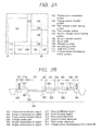
- FIGS. 2A and 2B illustrate a top view and a sectional view of a solid-state imaging apparatus according to the present embodiment, respectively. Portions having similar functions to those in FIG. 1 have the same reference numerals/characters and detailed description will not be repeated.
- each region is rectangular for easy description, which indicates that each configuration is not always rectangular and, in the region, at least the each configuration is disposed. Other embodiments are applicable in the same way. Only one pixel is illustrated, however, such a plurality of pixels is disposed to constitute a pixel region.
- the first charge carrier holding portion 103 is disposed in a first direction (right-hand in Figure) relative to the photoelectric conversion portion 101 .
- the FD region 107 is arranged in a second direction (downward in Figure) orthogonal to the first direction, relative to the first charge carrier holding portion 103 .
- FIG. 2B illustrates a sectional view taken along line 2 B- 2 B in FIG. 2A .
- the p-type semiconductor region 301 can be formed by injecting a p-type impurity ion into an n-type semiconductor substrate. Otherwise, a p-type semiconductor substrate may be used.
- the n-type semiconductor region (a first semiconductor region of a first conductivity type) 302 constitutes a part of the photoelectric conversion portion and has the same polarity as an electron which is a signal carrier, where a PN junction is constituted with the p-type semiconductor region 301 (a second semiconductor region of a second conductivity type).
- the p-type semiconductor region 303 provided on a surface of the n-type semiconductor region 302 to use an embedded type photodiode as the photoelectric conversion portion, suppresses an adverse effect of an interface state and a dark current generated on a surface of the photoelectric conversion portion.
- the photoelectric conversion portion includes at least the p-type semiconductor region 301 and the n-type semiconductor region 302 constituting a PN junction with the p-type semiconductor region 301 .
- the charge carrier path 304 is between the n-type semiconductor region 302 and an n-type semiconductor region 305 to be described later, where an n-type impurity with low concentration is doped to constitute a buried channel structure.
- the n-type semiconductor region (a third semiconductor region of the first conductivity type) 305 constitutes a part of the first charge carrier holding portion 103 and is configured to accumulate a charge transferred from the photoelectric conversion portion 101 for a fixed period.
- the n-type semiconductor region (a fourth semiconductor region of a first conductivity type) 306 constitutes a part of the second charge carrier accumulating portion 105 and is configured to accumulate a charge transferred from the first charge carrier holding portion 103 for a fixed period.
- the first conductivity type floating diffusion region (FD region) 307 functions as a charge carrier-to-voltage conversion portion and is electrically connected with a gate of an amplifying MOS transistor through a plug or the like.
- the overflow drain region 308 is a first conductivity type OFD region.
- the first control electrode 309 is disposed on the third semiconductor region 305 through an insulation film and can control a potential state of a region in proximity to an interface of the insulation film on the third semiconductor region 305 .
- the first charge carrier holding portion 103 includes the n-type semiconductor region 305 and the first control electrode 309 .
- the first control electrode 309 is disposed, extending to the n-type semiconductor region 304 and has a function as a transfer electrode, which may be provided separately from each other.
- the second control electrode 310 is arranged on the fourth semiconductor region 306 through an insulation film and can control a potential state of a region in proximity to an interface of the insulation film on the fourth semiconductor region 306 .
- the second charge carrier holding portion 105 includes the n-type semiconductor region 306 and the second control electrode 310 .
- the second control electrode 310 is disposed, extending to the n-type semiconductor regions 305 , 306 and has a function as a transfer electrode, which may be provided separately from each other.
- the third control electrode 311 is configured to control a potential state of a charge carrier path between the n-type semiconductor region 306 and the FD region 307 .
- the charge carrier discharging control electrode 312 is configured to control a potential of a charge carrier path between the n-type semiconductor region 302 and the OFD region 308 constituting the photoelectric conversion portion.
- FIG. 3 illustrates a progress in time series of a driving pulse supplied to each of the control electrode and the transfer electrode in FIGS. 1 , 2 A and 2 B.
- Reference numerals/characters are the same as those in FIGS. 2A and 2B .
- Suffixes of respective control lines show (n)th, (n+1)th and (n+2)th rows. Description will be made on only three rows herein, however, the present invention is applicable to a case of more than three rows by repeating the driving pattern and is highly active.
- a pulse which keeps the second transfer portion of each pixel row to be in an electrical connection state is supplied in the order of ⁇ 311 ( n ), ⁇ 311 ( n+ 1) and ⁇ 311 ( n+ 2) and thereby the charge carrier held by the second charge carrier holding portion is transferred to an input portion of an amplifying portion and the selection portion is brought into an electrical connection to read out a signal to the outside.
- This is a first frame reading-out operation.
- light is launched into the photoelectric conversion portion for photoelectric conversion, thus creating a second frame accumulating period.
- a second frame signal carrier is accumulated in the photoelectric conversion portion and the first charge carrier holding portion.
- ⁇ 309 is concurrently brought into electrical connection for all pixel rows to complete the second frame accumulating period.
- ⁇ 312 is concurrently brought into electrical connection for all pixel rows, thus creating a discharging period for discharging the charge carrier generated by the photoelectric conversion portion to the OFD region.
- ⁇ 310 is brought into electrical connection in a collective manner and the signal carrier of the second frame held by the first charge carrier holding portion is transferred to the second charge carrier holding portion.
- ⁇ 311 is brought into electrical connection in row order and charge carrier transfer is made from the second charge carrier holding portion to the input node of the amplifying portion.
- the present embodiment provides shooting by an electronic shutter operation without any break of shooting time in such a configuration that a signal carrier moves and is accumulated in the charge carrier holding portion during an exposure period.
- a difference of the present embodiment from the first embodiment is that between charge carrier holding portions adaptable to a plurality of photoelectric conversion portions, there is disposed a charge carrier path through which charges are made movable therebetween.
- the present embodiment includes at least one charge carrier holding portion provided for each photoelectric conversion portion and is configured in such a manner that at least one charge carrier holding portion is shared by the plurality of photoelectric conversion portions or pixels. Such a configuration provides further reductions in an element area and a pixel pitch than the first embodiment.
- FIG. 4 illustrates an equivalent circuit diagram of a solid-state imaging apparatus according to the present embodiment. Suffixes “a” and “b” indicate that to which of photoelectric conversion portions illustrated in FIGS. 5A to 5C each configuration correspond.
- the photoelectric conversion portions 701 a , 701 b , the first transfer portions 702 a , 702 b , the first charge carrier holding portions 703 a , 703 b and the second transfer portion 704 When viewed from the photoelectric conversion portion 702 b , the first charge carrier holding portions 703 a , 703 b are connected in series through the second transfer portion 704 . Further, there are also provided the third transfer portion 706 , the input node of an amplifying portion 707 , the resetting portion 708 , the amplifying portion 709 and the selection portion 710 . A member having the same name as that in the first embodiment has a similar function and detailed description will not be repeated.
- FIG. 5A illustrates a top view of a solid-state imaging apparatus according to the present embodiment
- FIG. 5B illustrates a sectional view taken along line 5 B- 5 B in FIG. 5A
- FIG. 5C illustrates a sectional view taken along line 5 C- 5 C in FIG. 5A .
- the similar configurations to that in FIG. 4 have the same reference numerals/characters and detailed description will not be repeated.
- the first transfer portion 702 is disposed in a region between the photoelectric conversion portion 701 and the first charge carrier holding portion 703 .
- the first charge carrier holding portion 703 is provided for the respective photoelectric conversion portions.
- the second transfer portion 704 controls a potential of a charge carrier path between the two first charge carrier holding portions 703 a , 703 b .
- the second transfer portion 704 allows the first charge carrier holding portion 703 a adaptable to the first photoelectric conversion portion 701 a to be used as a second charge carrier holding portion in reading out a signal based on a signal carrier generated by the second photoelectric conversion portion 701 b .
- the control electrode 313 constitutes a second transfer portion.
- control electrode 313 constituting the second transfer portion 704 is provided, electrically separated from a control electrode 309 a .
- a potential state of a charge carrier path between the first charge carrier holding portion 703 a and the second charge carrier holding portion 703 b is controllable. More specifically, a potential state of a semiconductor region between n-type semiconductor regions 305 , 306 is controlled.
- Each supply pulse is a pulse supplied to each control electrode in FIGS. 5A to 5C .
- the suffix “n” is the number of pixel rows, where a unit constituted by disposing a plurality of units including two photoelectric conversion portions perpendicularly adjacent to each other in a horizontal direction is taken as one pixel row. Use of a plurality of more rows is applicable by repeating the driving pattern, which is highly active.
- a first-frame signal is accumulated in the second charge carrier holding portion 703 b .
- the charge carrier held by the second charge carrier holding portion is transferred to an input portion of the amplifying portion.
- a selection portion By bringing a selection portion into electrical connection, a signal is read out to the outside. This is a first-frame reading-out operation. Description will be made on ⁇ 312 supplied to a charge carrier discharge control electrode during a first-frame reading-out period.
- ⁇ 312 a that is, a charge carrier discharging control portion adaptable to a first photoelectric conversion portion is in a non-conduction state
- ⁇ 312 b that is, the charge carrier discharging control portion adaptable to a second photoelectric conversion portion is in an electrical connection state
- the signal carrier generated by the first photoelectric conversion portion is in a usable state as an image signal
- the signal carrier generated by the second photoelectric conversion portion 701 b is in a discharging state to an OFD region.
- the signal carrier generated by the first photoelectric conversion portion 701 a is used as a second-frame image signal.
- ⁇ 309 a is brought into electrical connection in a collective manner and charge carriers of the first photoelectric conversion portion 701 a are transferred to the first charge carrier holding portion 703 a .
- a charge carrier discharging control portion 312 a adaptable to the first photoelectric conversion portion 701 a is brought into electrical connection. Because all charge carrier discharging control portions are in an electrical connection state, the signal carrier generated during this period is discharged to the OFD region.
- ⁇ 313 By bringing ⁇ 313 into electrical connection after lapse of a predetermined period, a charge carrier of the first charge carrier holding portion 703 a is transferred to the second charge carrier holding portion 703 b . At this time, ⁇ 309 b is also concurrently brought into electrical connection. Subsequently, by sequentially bringing ⁇ 311 into electrical connection, a charge carrier is transferred to the input portion of the amplifying portion. By bringing the selection portion into electrical connection, a signal is read out to the outside. This is a second-frame reading-out operation. During a period at which ⁇ 311 is sequentially brought into electrical connection, ⁇ 309 and ⁇ 312 a are brought into electrical connection in order.
- This operation can determine accumulating periods of the first photoelectric conversion portion 701 a and the first charge carrier holding portion 702 a . Specifically, it is sufficient to change a timing for bringing ⁇ 309 and ⁇ 312 a into electrical connection, depending upon an accumulating period of each frame. Continuous implementation of such operations allows moving image shooting.
- shooting is made, using a signal carrier generated by at least either one of the two photoelectric conversion portions.
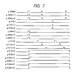
- FIG. 7 illustrates other driving methods using configurations in FIGS. 4 and 5A to 5 C.
- all the signal carriers generated by the second photoelectric conversion portion are discharged to the OFD region by the charge carrier discharging control portion, however, in FIG. 7 , the signal carrier generated by the second photoelectric conversion portion is used as a signal for image.
- ⁇ 312 kept in a non-conduction state, charges are accumulated, using the first and the second photoelectric conversion portions and the first charge carrier holding portion.
- ⁇ 309 By bringing ⁇ 309 into electrical connection in a collective manner after lapse of predetermined period, charge transfer is made from the photoelectric conversion portion to the first charge carrier holding portion and concurrently ⁇ 312 is brought into electrical connection and the charge generated by the photoelectric conversion portion is discharged to the OFD region.
- ⁇ 311 By sequentially bringing ⁇ 311 into electrical connection, a signal based on the signal carrier generated by the second photoelectric conversion portion is read out.
- ⁇ 313 has been brought into electrical connection after completion of the reading-out, ⁇ 311 is sequentially brought into electrical connection again to read out a signal based on the signal carrier generated by the first photoelectric conversion portion.
- a driving method in FIG. 7 provides higher-quality shooting than in FIG. 6 because signals of all the photoelectric conversion portions are available. Accordingly, the driving method is suitable, particularly in performing still image shooting.
- the driving methods in FIGS. 6 and 7 if configured in a solid-state imaging apparatus to have a first drive mode and a second drive mode and to be switchable therebetween as needed, provides shooting suitable for both a moving image and a still image.
- the present invention provides continuous moving image shooting while, for example, suppressing noise from being mixed into a charge carrier holding portion provided in a pixel.
- FIG. 8 is an equivalent circuit diagram of a solid-state imaging apparatus according to the present embodiment and illustrates 4 pixels, however, the solid-state imaging apparatus may be configured to have a plurality of more pixels.
- the photoelectric conversion portion 801 illustrates a photodiode as an example.
- the output node O-node is an output node of the photoelectric conversion portion.
- the first and the second charge carrier transfer portion 802 , 803 are configured to transfer a signal carrier generated in the photoelectric conversion portion 801 to a circuit element at a subsequent stage.
- the charge carrier discharging control portion 804 is capable of discharging charges of a photoelectric conversion portion 801 and may use, for example, a MOS transistor as the photoelectric conversion portion.
- the carrier discharging control portion is configured in such a manner that a semiconductor region having the same polarity as a signal carrier constituting a part of the photoelectric conversion portion is taken as a source and a semiconductor region (overflow drain region: OFD region) 805 supplied with a power supply voltage is taken as drain.
- the first and the second charge carrier holding portions 806 , 807 are configured to hold a signal carrier generated in the photoelectric conversion portion.
- the first and the second charge transfer portion 808 , 809 are configured to transfer charges held by the first and the second charge carrier holding portions to a circuit element at a subsequent stage.
- the input node 810 is an input node of an amplifying portion to be described later and is configured to hold charges to be transferred through the first and the second transfer portions from the first and the second charge carrier holding portions.
- the input node can use, for example, a floating diffusion region (FD region) distributed to a semiconductor substrate.
- the resetting portion 811 is configured to supply a reference voltage to the input node 810 of the amplifying portion.
- the amplifying portion 812 amplifies a signal based on a signal carrier transferred to the FD region and reads out the amplified signal to the outside.
- a signal carrier transferred to the FD region
- the amplifying portion may use such a configuration that a gate of the MOS transistor and the FD region are electrically connected to each other.
- the selection portion 813 is configured to select each pixel and read the selected pixel to the outside for each pixel or for each pixel row.
- Each of the transfer portion, the resetting portion, the selection portion and the charge carrier discharging control portion may use a MOS transistor.
- the present embodiment is characterized by a structure of a charge carrier path between the photoelectric conversion portion and the first and the second charge carrier holding portions.
- the present embodiment is configured to transfer a charge from the photoelectric conversion portion to the first and the second charge carrier holding portions with such a voltage as to cause the first and the second charge transfer portions to be in a non-conduction state being supplied.
- the charge carrier transfer portion is of a MOS transistor.
- the MOS transistor constitutes a buried channel structure.
- This configuration includes a portion in which an energy barrier is positioned to be lower even under a non-conduction state.
- the charge carrier transfer portion can also keep a constant voltage to be in a supplied state without any positive control.
- a stationary potential barrier may be provided without need of having a function serving as the transfer portion.
- Such a configuration allows most of signal carriers generated by photoelectric conversion when light is launched into the photoelectric conversion portion to be transferred to the first charge carrier holding portion without any accumulation in the photoelectric conversion portion. Accordingly, the photoelectric conversion portion included in all pixels allows charge accumulation time to be unified.
- the MOS transistor When the MOS transistor is in a non-conduction state, a hole is accumulated in a channel surface and a channel to which a charge current is transferred exists in a portion at a predetermined depth from the surface and therefore an adverse effect of a dark current can be suppressed at an insulation film interface.
- a potential of a charge carrier path between the photoelectric conversion portion and the charge carrier holding portion is lower than that of a charge carrier path between the photoelectric conversion portion and an OFD region.
- the potential used herein is a potential for a signal carrier.
- a charge moved to at least either one of the first and the second charge carrier holding portions from the photoelectric conversion portion during one exposure period is held and used as an image signal.
- a signal is read out to the outside of a pixel without any reset operation of the charge carrier holding portion.
- One exposure period used herein refers to the one determined in common by the each photoelectric conversion portion when a one-frame image is taken.
- the plurality of charge carrier holding portions are provided for one photoelectric conversion portion 801 and charge holding is performed, using charge carrier holding portions different for each frame, thus attaining continuous moving image shooting.
- the charge carrier holding portion may have a state where a signal carrier of a previous frame is held. This is because the signal carrier is required to be held for a fixed period by the charge carrier holding portion until a selection operation is performed for reading out to the outside for each pixel row.
- the mixed charge is a charge generated during a period which is not an original exposure period (a charge of a following frame), which causes a noise.
- the charge carrier discharging control portion requires to discharge a signal carrier generated by the photoelectric conversion portion to an OFD region. Hence, mixing of a charge into the charge carrier holding portion can be inhibited. However, if such an operation is performed, such a state where image information is missing will be made during a period at which a charge carrier is being discharged by the charge carrier discharging control portion. Therefore, a moving image tends to be taken with discontinuous frame.
- installation of a plurality of charge carrier holding portions (a first and a second charge carrier holding portions) in the photoelectric conversion portion allows continuous moving image shooting. Specifically, during a period at which charges generated by the photoelectric conversion portion are held by the photoelectric conversion portion and the first charge carrier holding portion, the second charge carrier holding portion can hold charges until a pixel row is sequentially selected.
- FIGS. 9A , 9 B and 9 C illustrate a top view and sectional views of a solid-state imaging apparatus according to the present embodiment. Portions having similar functions to those in FIG. 8 have the same reference numerals/characters and detailed description will not be repeated.
- each region is rectangular for easy description, which indicates that each configuration is not always rectangular and, in the region, at least the each configuration is disposed. Other embodiments are applicable in the same way. Only one pixel is illustrated, however, such a plurality of pixels is disposed to constitute a pixel region.
- the first charge carrier holding portion 806 is disposed, adjacent to the photoelectric conversion portion 801 in the first direction (downward in Figure), while the second charge carrier holding portion 807 is disposed, adjacent to the photoelectric conversion portion in the second direction (to the right in Figure) orthogonal to the first direction.
- Such a configuration can attain efficient arrangement of respective elements and reduction in a pixel pitch.
- FIG. 9B is a sectional view taken along line 9 B- 9 B in FIG. 9A
- FIG. 9C is a sectional view taken along line 9 C- 9 C in FIG. 9A .
- the p-type semiconductor region 901 can be formed by injecting a p-type impurity ion into an n-type semiconductor substrate. Otherwise, a p-type semiconductor substrate may be used.
- the n-type semiconductor region (a first semiconductor region of a first conductivity type) 902 constitutes a part of the photoelectric conversion portion and has the same polarity as an electron which is a signal carrier, where a PN junction is constituted with the p-type semiconductor region 901 (a second semiconductor region of a second conductivity type).
- the p-type semiconductor region 903 is provided on a surface of the n-type semiconductor region 902 and provided to use an embedded type photodiode as the photoelectric conversion portion, which suppresses an adverse effect of an interface state and a dark current generated on a surface of the photoelectric conversion portion.
- the photoelectric conversion portion includes at least the p-type semiconductor region 901 and the n-type semiconductor region 902 constituting a PN junction with the p-type semiconductor region 901 .
- the charge carrier path 904 a , 904 b are between the n-type semiconductor region 902 and n-type semiconductor regions 905 a , 905 b to be described later, where an n-type impurity with low concentration is doped to constitute a buried channel structure.
- the n-type semiconductor regions (third and fourth semiconductor regions of a first conductivity type) 905 a , 905 b constitute a part of the first and the second charge carrier holding portions 806 , 807 and are configured to store a charge transferred from the photoelectric conversion portion 101 for a fixed period.
- the first conductivity type floating diffusion region (FD region) 906 functions as a charge voltage conversion portion and is electrically connected with a gate of an amplifying MOS transistor through a plug.
- the overflow drain region 909 is a first conductivity type OFD region.
- the first control electrode 907 a is disposed on the n-type semiconductor region 905 a through an insulation film and can control a potential state of a region in proximity to an insulation film interface, of the n-type semiconductor region 905 a .
- the first charge carrier holding portion 806 includes the n-type semiconductor region 905 a and the first control electrode 907 a.
- the first control electrode 907 a is disposed, extending to the n-type semiconductor region 904 a and has a function as a transfer electrode, which may be provided separately from each other.
- the second control electrode 907 b is disposed on the n-type semiconductor region 905 b through an insulation film and can control a potential state of a region in proximity to an interface of the insulation film on the n-type semiconductor region 905 b .
- the second charge carrier holding portion 807 includes the n-type semiconductor region 905 b and the second control electrode 907 b.
- the second control electrode 907 b is disposed, extending to the n-type semiconductor region 904 b and has a function as a transfer electrode, which may be provided separately from each other.
- the third and the fourth control electrodes 908 a , 908 b are configured to control a potential state of a charge carrier path between the n-type semiconductor regions 905 a , 905 b and the FD region 906 .
- the charge carrier discharging control portion 910 is configured to control a potential of a charge carrier path between the n-type semiconductor region 902 and the OFD region 909 constituting the photoelectric conversion portion.
- FIG. 10 illustrates a progress in time series of a driving pulse supplied to each of the control electrode and the transfer electrode in FIGS. 8 and 9A to 9 C.
- Reference numerals/characters are the same as those in FIGS. 9A to 9C .
- Suffixes of respective control lines show (n)th, (n+1)th and (n+2)th rows. Description will be made on only three rows herein, however, the present invention is applicable to a case of more than three rows by repeating the driving pattern and is highly active.
- the present embodiment is configured to give pulses of three values to ⁇ 802 . A first pulse, a second pulse and a third pulse are used in the order of pulse height.
- initial states are completion of 1st-frame accumulating period and charges being held by the second charge carrier holding portion.
- a first pulse is supplied to ⁇ 802 in all rows and a conduction pulse is supplied to ⁇ 808 and ⁇ 804 .
- This operation discharges charges of the photoelectric conversion portion and the first charge carrier holding portion to the OFD region.
- a resetting portion (not illustrated) into electrical connection
- charges of the FD region 810 and the first charge carrier holding portion may be discharged to a resetting power supply.
- a third pulse is supplied to ⁇ 803 and the second charge transfer portion 803 is in a non-conduction state.
- a second pulse is supplied to ⁇ 802 and a pulse to be brought into electrical non-conduction is supplied to ⁇ 808 .
- This operation starts accumulation of 2nd-frame signal carriers in the photoelectric conversion portion and the first charge carrier holding portion.
- a charge carrier path in the first charge transfer portion exists in a region buried inside a substrate at a predetermined distance from a surface (Buried channel).
- a conduction pulse is supplied to ⁇ 809 in row order.
- a signal carrier held by the second charge carrier holding portion is transferred to an input portion of the amplifying portion to bring the selection portion into electrical connection, thus reading out a signal to the outside.
- This is a first frame reading-out operation. As described above, during 1st-frame reading-out operation, light is launched into the photoelectric conversion portion for photoelectric conversion, which reaches 2nd-frame accumulating period.
- a first pulse is supplied to ⁇ 802 in all rows and 2nd-frame signal carrier left in the photoelectric conversion portion is transferred to the first charge carrier holding portion in a collective manner. This operation completes the 2nd-frame accumulating period.
- a conduction pulse is supplied to ⁇ 804 .
- ⁇ 804 is kept in electrical connection until a 3rd-frame accumulating start period. The electrical connection period of ⁇ 804 may be changed depending upon the accumulating period (exposure period) of each frame.
- a conduction pulse is supplied to ⁇ 808 in row order.
- This operation transfers a signal carrier held by the first charge carrier holding portion to an input portion of the amplifying portion and reads out a signal by bringing the selection portion into electrical connection.
- This is a 2nd frame reading-out operation.
- 2nd-frame reading-out operation period light is launched into the photoelectric conversion portion for photoelectric conversion, thus taking a 3rd-frame accumulating period.
- the 3rd-frame accumulation is started by supplying a non-conduction pulse to ⁇ 804 , a second pulse to ⁇ 803 and a non-conduction pulse to ⁇ 809 after supplying a first pulse to ⁇ 803 and a conduction pulse to ⁇ 809 , respectively.
- a charge carrier path in the second charge transfer portion exists in a region buried inside a substrate at a predetermined distance from a surface (Buried channel).
- the accumulating period of each frame can be set as needed from conduction periods of ⁇ 104 and ⁇ 804 .
- FIG. 4 illustrates an example used as an image signal by adding charges held by the first and the second charge carrier holding portions.
- a ternary pulse was supplied to ⁇ 802 , ⁇ 803 , however, a binary pulse may be used in this example.
- a first pulse and a second pulse are taken in descending order of pulse height.
- a first pulse is supplied to ⁇ 802 and ⁇ 803 and a conduction pulse is supplied to ⁇ 808 , ⁇ 809 and ⁇ 804 .
- a second pulse is supplied to ⁇ 802 , ⁇ 803 and a non-conduction pulse is supplied to ⁇ 808 , ⁇ 809 and ⁇ 810 .
- This operation allows the photoelectric conversion portion, the first charge carrier holding portion and the second charge carrier holding portion to store a signal carrier.
- a first pulse is supplied to ⁇ 802 , ⁇ 803 and a signal carrier left in the photoelectric conversion portion is transferred to the each charge carrier holding portion.
- Driving methods in FIGS. 10 and 11 can be used by switching, for example, in switching moving image shooting and still image shooting.
- FIGS. 5A to 5C and 12 illustrate an equivalent circuit diagram of a solid-state imaging apparatus according to the present embodiment.
- the difference from the first embodiment is that an output node of a first photoelectric conversion portion is electrically connectable with a plurality of charge carrier holding portions through a transfer portion. That is, a first charge carrier holding portion provided corresponding to a second photoelectric conversion portion can be used as a second charge carrier holding portion of the first photoelectric conversion portion.
- one set of operations is made in two pixel rows and a charge generated by the photoelectric conversion portion in one row is always discharged though an OFD.
- FIGS. 5A to 5C and 12 there are the first photoelectric conversion portions 501 a , 1201 a and the second photoelectric conversion portions 501 b , 1201 b .
- the charge carrier holding portions 506 a , 1206 a are mounted corresponding to the first photoelectric conversion portions 501 a , 1201 a .
- the charge carrier holding portions 506 b , 1206 b are mounted corresponding to the second photoelectric conversion portions 501 b , 1201 b .
- the reference characters 506 a , 1206 a are taken as the first charge carrier holding portions and the reference characters 506 b , 1206 b are taken as the second charge carrier holding portions.
- First charge carrier transfer portions 502 a , 1202 a are arranged between output nodes O-nodes of the first photoelectric conversion portions 501 a , 1201 a and the first charge carrier holding portions 506 a , 1206 a . Further, second charge carrier transfer portions 514 , 1214 are arranged between the output nodes O-nodes of the first photoelectric conversion portions 501 a , 1201 a and the second charge carrier holding portions 506 b , 1206 b . Arranging the second charge carrier transfer portions 514 , 1214 enables a signal carrier from the first photoelectric conversion portion to be held in the first and second charge carrier holding portions.
- This configuration allows a signal carrier in a first frame to be held in the first charge carrier holding portions 506 a , 1206 a and a signal carrier in a second frame after the first frame in terms of time to be held in the second charge carrier holding portion 506 b , 1206 b.
- charge carrier transfer portions 502 , 1202 there are the charge carrier transfer portions 502 , 1202 , charge carrier discharging control portions 504 , 1204 , OFD regions 505 , 1205 , charge carrier holding portions 506 , 1206 , first transfer portions 508 , 1208 , FD regions 510 , 1210 , resetting portions 511 , 1211 , amplifying portions 512 , 1212 and selection portions 513 , 1213 .
- a suffix “a” is added to the configuration provided corresponding to the first photoelectric conversion portions and a suffix b is added to the configuration provided corresponding to the second photoelectric conversion portions. No suffix is added to a configuration commonly provided on the first and second photoelectric conversion portions.
- Each of the configurations has a similar function to that of the first embodiment.
- FIGS. 6 and 13 are a top view and a sectional view of a solid-state imaging apparatus according to the present embodiment. Portions having similar functions to those in FIGS. 5A to 5C and 12 have the same reference numerals/characters and detailed description will not be repeated.
- the first charge carrier holding portions 506 a , 1206 a and the second charge carrier holding portions 506 b , 1206 b are arranged through the charge carrier transfer portions in the vertical directions of the drawings for the first photoelectric conversion portions 501 a , 1201 a.
- the charge carrier transfer portions 502 a , 1202 a , 1202 b , 1114 , 1214 are doped with n-type impurities with low concentration to constitute a buried channel structure.
- FIGS. 7 and 14 a drive method for the solid-state imaging apparatus according to the present embodiment will be described. Differences from the embodiments described above will be mainly described and overlapped description will not be repeated.
- a ternary pulse can be supplied to ⁇ 1202 a , ⁇ 1214 in FIG. 3 , respectively.
- a first-frame signal is held in the second charge carrier holding portion and a second-frame signal is held in the first charge carrier holding portion.
- a third pulse is supplied to ⁇ 1202 b , ⁇ 1214 and is strongly turned off and hence a charge carrier will not flow into the second charge carrier holding portion.
- a second pulse is supplied to ⁇ 1202 a and hence a charge carrier generated by the photoelectric conversion portion flow into the first charge carrier holding portion.
- a pulse is sequentially supplied to ⁇ 1208 b for each row and a charge carrier of the charge carrier holding portion is transferred to the FD region.
- the resetting portion is brought into electrical connection to reset the charge carrier in the FD region.
- a third pulse is supplied to ⁇ 1202 a and strongly turned off, while a second pulse is supplied to ⁇ 1214 and a charge carrier in the third frame is accumulated in the second charge carrier holding portion.
- a pulse is sequentially supplied to ⁇ 1208 a for each row and a second-frame frame charge carrier held by the first charge carrier holding portion is transferred to the FD region.
- drive in FIG. 14 and drive using the first and second charge carrier holding portions for charge carrier holding in respective photoelectric conversion portions may be selectively used.
- drive in FIG. 14 is used for obtaining a moving image, while drive using the first and second charge carrier holding portions for charge carrier holding in the photoelectric conversion portions respectively corresponding to is used in such a case as to require high resolution like still-flame pictures.
- charge carriers generated by the two photoelectric conversion portions may be added by supplying a pulse in synchronization with the ⁇ 1202 a , ⁇ 1202 b to the ⁇ 1214 .
Applications Claiming Priority (3)
| Application Number | Priority Date | Filing Date | Title |
|---|---|---|---|
| JP2008-120408 | 2008-05-02 | ||
| JP2008120408 | 2008-05-02 | ||
| PCT/JP2009/058791 WO2009133967A2 (en) | 2008-05-02 | 2009-04-30 | Solid-state imaging apparatus |
Related Parent Applications (1)
| Application Number | Title | Priority Date | Filing Date |
|---|---|---|---|
| PCT/JP2009/058791 A-371-Of-International WO2009133967A2 (en) | 2008-05-02 | 2009-04-30 | Solid-state imaging apparatus |
Related Child Applications (1)
| Application Number | Title | Priority Date | Filing Date |
|---|---|---|---|
| US13/832,283 Division US9083908B2 (en) | 2008-05-02 | 2013-03-15 | Solid-state imaging apparatus with each pixel including a photoelectric conversion portion and plural holding portions |
Publications (2)
| Publication Number | Publication Date |
|---|---|
| US20110007196A1 US20110007196A1 (en) | 2011-01-13 |
| US8625010B2 true US8625010B2 (en) | 2014-01-07 |
Family
ID=40996481
Family Applications (2)
| Application Number | Title | Priority Date | Filing Date |
|---|---|---|---|
| US12/933,471 Expired - Fee Related US8625010B2 (en) | 2008-05-02 | 2009-04-30 | Solid-state imaging apparatus with each pixel including a photoelectric converter portion and plural holding portions |
| US13/832,283 Expired - Fee Related US9083908B2 (en) | 2008-05-02 | 2013-03-15 | Solid-state imaging apparatus with each pixel including a photoelectric conversion portion and plural holding portions |
Family Applications After (1)
| Application Number | Title | Priority Date | Filing Date |
|---|---|---|---|
| US13/832,283 Expired - Fee Related US9083908B2 (en) | 2008-05-02 | 2013-03-15 | Solid-state imaging apparatus with each pixel including a photoelectric conversion portion and plural holding portions |
Country Status (4)
| Country | Link |
|---|---|
| US (2) | US8625010B2 (zh) |
| JP (1) | JP5235774B2 (zh) |
| CN (1) | CN102017150B (zh) |
| WO (1) | WO2009133967A2 (zh) |
Cited By (3)
| Publication number | Priority date | Publication date | Assignee | Title |
|---|---|---|---|---|
| US9398236B2 (en) | 2013-11-18 | 2016-07-19 | Canon Kabushiki Kaisha | Image capturing apparatus |
| US10165215B2 (en) | 2015-07-28 | 2018-12-25 | Canon Kabushiki Kaisha | Imaging apparatus and control method for solid-state image sensor |
| US20230052637A1 (en) * | 2020-01-29 | 2023-02-16 | Sony Semiconductor Solutions Corporation | Solid-state imaging device, method of driving solid-state imaging device, and electronic device |
Families Citing this family (47)
| Publication number | Priority date | Publication date | Assignee | Title |
|---|---|---|---|---|
| JP4494492B2 (ja) * | 2008-04-09 | 2010-06-30 | キヤノン株式会社 | 固体撮像装置及び固体撮像装置の駆動方法 |
| JP5625284B2 (ja) * | 2009-08-10 | 2014-11-19 | ソニー株式会社 | 固体撮像装置、固体撮像装置の駆動方法および電子機器 |
| JP5630991B2 (ja) | 2009-12-14 | 2014-11-26 | キヤノン株式会社 | 撮像装置 |
| WO2011096340A1 (ja) * | 2010-02-05 | 2011-08-11 | 国立大学法人静岡大学 | 固体撮像装置、画素信号を読み出す方法、画素 |
| JP5516960B2 (ja) * | 2010-04-02 | 2014-06-11 | ソニー株式会社 | 固体撮像装置、固体撮像装置の駆動方法、および、電子機器 |
| JP5631643B2 (ja) * | 2010-06-24 | 2014-11-26 | オリンパス株式会社 | 読出制御装置、読出制御方法、撮像装置、固体撮像装置およびプログラム |
| JP5885401B2 (ja) | 2010-07-07 | 2016-03-15 | キヤノン株式会社 | 固体撮像装置および撮像システム |
| JP5697371B2 (ja) | 2010-07-07 | 2015-04-08 | キヤノン株式会社 | 固体撮像装置および撮像システム |
| JP5656484B2 (ja) | 2010-07-07 | 2015-01-21 | キヤノン株式会社 | 固体撮像装置および撮像システム |
| JP5643555B2 (ja) | 2010-07-07 | 2014-12-17 | キヤノン株式会社 | 固体撮像装置及び撮像システム |
| JP5751766B2 (ja) * | 2010-07-07 | 2015-07-22 | キヤノン株式会社 | 固体撮像装置および撮像システム |
| JP5456644B2 (ja) * | 2010-11-17 | 2014-04-02 | 本田技研工業株式会社 | 受光素子及び制御方法 |
| TWI505453B (zh) * | 2011-07-12 | 2015-10-21 | Sony Corp | 固態成像裝置,用於驅動其之方法,用於製造其之方法,及電子裝置 |
| US9118883B2 (en) * | 2011-11-28 | 2015-08-25 | Semiconductor Components Industries, Llc | High dynamic range imaging with multi-storage pixels |
| JP2013162148A (ja) * | 2012-02-01 | 2013-08-19 | Sony Corp | 個体撮像装置および駆動方法、並びに電子機器 |
| US9490373B2 (en) * | 2012-02-02 | 2016-11-08 | Sony Corporation | Solid-state imaging device and electronic apparatus with improved storage portion |
| JP5936386B2 (ja) * | 2012-02-17 | 2016-06-22 | キヤノン株式会社 | 撮像装置 |
| JP6012197B2 (ja) * | 2012-02-17 | 2016-10-25 | キヤノン株式会社 | 撮像装置及び撮像装置の駆動方法 |
| JP6012195B2 (ja) * | 2012-02-17 | 2016-10-25 | キヤノン株式会社 | 光電変換装置、および、光電変換装置の駆動方法 |
| JP6083934B2 (ja) * | 2012-02-17 | 2017-02-22 | キヤノン株式会社 | 光電変換装置の駆動方法 |
| JP5995457B2 (ja) | 2012-02-17 | 2016-09-21 | キヤノン株式会社 | 撮像装置、撮像システム、および撮像装置の駆動方法。 |
| FR3005205A1 (fr) | 2013-04-26 | 2014-10-31 | St Microelectronics Grenoble 2 | Capteur d'image a gain de conversion multiple |
| CN103491320B (zh) * | 2013-09-05 | 2017-02-08 | 北京立博信荣科技有限公司 | 一种图像传感电路及方法 |
| JP6376785B2 (ja) * | 2014-03-14 | 2018-08-22 | キヤノン株式会社 | 撮像装置、および、撮像システム |
| JP6374690B2 (ja) * | 2014-04-01 | 2018-08-15 | キヤノン株式会社 | 撮像装置及びその制御方法、プログラム、記憶媒体 |
| JP6452381B2 (ja) | 2014-10-23 | 2019-01-16 | キヤノン株式会社 | 撮像装置 |
| JP6508929B2 (ja) * | 2014-12-10 | 2019-05-08 | キヤノン株式会社 | 固体撮像装置及びその駆動方法 |
| US9912886B2 (en) | 2014-12-17 | 2018-03-06 | Canon Kabushiki Kaisha | Image capturing apparatus and driving method of image sensor |
| JP6502485B2 (ja) * | 2015-05-21 | 2019-04-17 | オリンパス株式会社 | 撮像装置 |
| US10341592B2 (en) | 2015-06-09 | 2019-07-02 | Sony Semiconductor Solutions Corporation | Imaging element, driving method, and electronic device |
| TWI701819B (zh) * | 2015-06-09 | 2020-08-11 | 日商索尼半導體解決方案公司 | 攝像元件、驅動方法及電子機器 |
| EP3109650B1 (en) * | 2015-06-25 | 2020-04-01 | ABB Schweiz AG | Signal handling for inaccessibly located power equipment |
| US10313600B2 (en) * | 2015-10-13 | 2019-06-04 | Canon Kabushiki Kaisha | Imaging device capable of simultaneously capturing of a motion image and a static image and imaging method |
| JP6727797B2 (ja) * | 2015-12-04 | 2020-07-22 | キヤノン株式会社 | 撮像装置の駆動方法 |
| JP2017135693A (ja) * | 2016-01-21 | 2017-08-03 | パナソニックIpマネジメント株式会社 | 撮像装置 |
| US10182199B2 (en) | 2016-02-22 | 2019-01-15 | Canon Kabushiki Kaisha | Imaging device and reproducing device |
| JP6890295B2 (ja) * | 2016-03-17 | 2021-06-18 | パナソニックIpマネジメント株式会社 | 撮像装置 |
| JP2017183563A (ja) * | 2016-03-31 | 2017-10-05 | ソニー株式会社 | 撮像装置、駆動方法、および、電子機器 |
| JP6667431B2 (ja) | 2016-12-27 | 2020-03-18 | キヤノン株式会社 | 撮像装置、撮像システム |
| FR3062519B1 (fr) * | 2017-01-31 | 2019-03-29 | Stmicroelectronics (Crolles 2) Sas | Capteur d'images a grande gamme dynamique et faible bruit |
| JPWO2019065866A1 (ja) * | 2017-09-29 | 2020-10-15 | 株式会社ニコン | 撮像素子 |
| JP7066392B2 (ja) * | 2017-12-14 | 2022-05-13 | キヤノン株式会社 | 撮像装置 |
| JP2019169501A (ja) | 2018-03-22 | 2019-10-03 | ソニーセミコンダクタソリューションズ株式会社 | 撮像素子及び電子機器 |
| JP2020053782A (ja) | 2018-09-26 | 2020-04-02 | ソニーセミコンダクタソリューションズ株式会社 | 固体撮像素子、および、撮像装置 |
| JP7458746B2 (ja) * | 2019-11-01 | 2024-04-01 | キヤノン株式会社 | 光電変換装置、撮像システム及び移動体 |
| US11627274B2 (en) * | 2021-04-16 | 2023-04-11 | Microsoft Technology Licensing, Llc | Image sensing pixels with lateral overflow storage |
| KR20230041388A (ko) * | 2021-09-17 | 2023-03-24 | 삼성전자주식회사 | 단위 픽셀, 이미지 센서 및 차량 |
Citations (23)
| Publication number | Priority date | Publication date | Assignee | Title |
|---|---|---|---|---|
| US4737854A (en) | 1986-07-18 | 1988-04-12 | Xerox Corporation | Image sensor array with two stage transfer |
| GB2270228A (en) | 1992-08-11 | 1994-03-02 | Mitsubishi Electric Corp | Infrared imaging array - speeding charge transfer. |
| US6040568A (en) * | 1998-05-06 | 2000-03-21 | Raytheon Company | Multipurpose readout integrated circuit with in cell adaptive non-uniformity correction and enhanced dynamic range |
| EP1098512A2 (en) | 1999-11-04 | 2001-05-09 | Taiwan Advanced Sensors Corporation | Pixel design for interlaced reading for high sensitivity CMOS image sensors |
| US20010007471A1 (en) * | 1998-02-27 | 2001-07-12 | Beiley Mark A. | Method to reduce reset noise in photodiode based CMOS image sensors |
| WO2002029895A1 (en) | 2000-09-29 | 2002-04-11 | Rockwell Scientific Company | Adaptive amplifier circuit with enhanced dynamic range |
| US20040051801A1 (en) * | 2002-09-18 | 2004-03-18 | Tetsuya Iizuka | Solid-state image pickup device and device driving control method for solid-state image pickup |
| JP2004087898A (ja) | 2002-08-28 | 2004-03-18 | Fujitsu Ltd | 画像信号読み出し回路 |
| US20050052554A1 (en) | 1998-11-27 | 2005-03-10 | Canon Kabushiki Kaisha | Solid-state image pickup apparatus |
| US20050110884A1 (en) | 2003-11-26 | 2005-05-26 | Altice Peter P.Jr. | Image sensor with a capacitive storage node linked to transfer gate |
| US20050219884A1 (en) * | 2004-03-30 | 2005-10-06 | Sohei Manabe | Hybrid charge coupled CMOS image sensor |
| JP2006217410A (ja) | 2005-02-04 | 2006-08-17 | Tohoku Univ | 光センサおよび固体撮像装置 |
| JP2006246450A (ja) | 2005-02-04 | 2006-09-14 | Canon Inc | 撮像装置及び撮像システム |
| JP2006262070A (ja) | 2005-03-17 | 2006-09-28 | Sharp Corp | 光電変換装置及びcmosイメージセンサ |
| US7116365B1 (en) * | 1998-06-08 | 2006-10-03 | Sony Corporation | Solid-state imaging element, method for driving the same, and camera system |
| US20060266922A1 (en) * | 2005-05-27 | 2006-11-30 | Eastman Kodak Company | Pinned-photodiode pixel with global shutter |
| US7227206B2 (en) | 2003-05-15 | 2007-06-05 | Canon Kabushiki Kaisha | Solid-state image sensor, production method for solid-state image sensor, and camera using solid-state image sensor |
| WO2008027193A2 (en) | 2006-08-29 | 2008-03-06 | Micron Technology, Inc. | Skimmed charge capture and charge packet removal for increased effective pixel photosensor full well capacity |
| US20080084489A1 (en) | 2006-10-04 | 2008-04-10 | Canon Kabushiki Kaisha | Photoelectric conversion apparatus provided with arrangement of plurality of pixels each having plurality of photoelectric conversion devices and accumulating unit for temporarily accumulating charges accumulated in plurality of photoelectric conversion devices |
| US20090015690A1 (en) | 2007-07-09 | 2009-01-15 | Canon Kabushiki Kaisha | Imaging apparatus and imaging method |
| US7569868B2 (en) | 2005-06-09 | 2009-08-04 | Canon Kabushiki Kaisha | Image pickup device and image pickup system |
| US20090219418A1 (en) * | 2008-02-29 | 2009-09-03 | Hiroaki Fujita | Image sensor and method to reduce dark current of cmos image sensor |
| US20090251582A1 (en) * | 2008-04-03 | 2009-10-08 | Sony Corporation | Solid state imaging device, driving method of the solid state imaging device, and electronic equipment |
Family Cites Families (7)
| Publication number | Priority date | Publication date | Assignee | Title |
|---|---|---|---|---|
| JP4761491B2 (ja) * | 2001-06-06 | 2011-08-31 | キヤノン株式会社 | 固体撮像装置及びそれを用いた撮像システム |
| JP2007166238A (ja) * | 2005-12-14 | 2007-06-28 | Victor Co Of Japan Ltd | 画素別シャッタ機能付cmosセンサ |
| JP5076528B2 (ja) * | 2007-02-06 | 2012-11-21 | 株式会社ニコン | 光電変換部の連結/分離構造、固体撮像素子及び撮像装置 |
| US8130302B2 (en) * | 2008-11-07 | 2012-03-06 | Aptina Imaging Corporation | Methods and apparatus providing selective binning of pixel circuits |
| JP5537172B2 (ja) * | 2010-01-28 | 2014-07-02 | ソニー株式会社 | 固体撮像装置及び電子機器 |
| JP2011159757A (ja) * | 2010-01-29 | 2011-08-18 | Sony Corp | 固体撮像装置とその製造方法、固体撮像装置の駆動方法、及び電子機器 |
| US8817154B2 (en) * | 2012-08-30 | 2014-08-26 | Omnivision Technologies, Inc. | Image sensor with fixed potential output transistor |
-
2009
- 2009-04-30 CN CN200980115090.6A patent/CN102017150B/zh not_active Expired - Fee Related
- 2009-04-30 WO PCT/JP2009/058791 patent/WO2009133967A2/en active Application Filing
- 2009-04-30 US US12/933,471 patent/US8625010B2/en not_active Expired - Fee Related
- 2009-05-01 JP JP2009112051A patent/JP5235774B2/ja active Active
-
2013
- 2013-03-15 US US13/832,283 patent/US9083908B2/en not_active Expired - Fee Related
Patent Citations (26)
| Publication number | Priority date | Publication date | Assignee | Title |
|---|---|---|---|---|
| US4737854A (en) | 1986-07-18 | 1988-04-12 | Xerox Corporation | Image sensor array with two stage transfer |
| GB2270228A (en) | 1992-08-11 | 1994-03-02 | Mitsubishi Electric Corp | Infrared imaging array - speeding charge transfer. |
| US5304803A (en) | 1992-08-11 | 1994-04-19 | Mitsubishi Denki Kabushiki Kaisha | Infrared imaging array |
| US20010007471A1 (en) * | 1998-02-27 | 2001-07-12 | Beiley Mark A. | Method to reduce reset noise in photodiode based CMOS image sensors |
| US6040568A (en) * | 1998-05-06 | 2000-03-21 | Raytheon Company | Multipurpose readout integrated circuit with in cell adaptive non-uniformity correction and enhanced dynamic range |
| US7116365B1 (en) * | 1998-06-08 | 2006-10-03 | Sony Corporation | Solid-state imaging element, method for driving the same, and camera system |
| US20050052554A1 (en) | 1998-11-27 | 2005-03-10 | Canon Kabushiki Kaisha | Solid-state image pickup apparatus |
| EP1098512A2 (en) | 1999-11-04 | 2001-05-09 | Taiwan Advanced Sensors Corporation | Pixel design for interlaced reading for high sensitivity CMOS image sensors |
| WO2002029895A1 (en) | 2000-09-29 | 2002-04-11 | Rockwell Scientific Company | Adaptive amplifier circuit with enhanced dynamic range |
| JP2004087898A (ja) | 2002-08-28 | 2004-03-18 | Fujitsu Ltd | 画像信号読み出し回路 |
| US20040051801A1 (en) * | 2002-09-18 | 2004-03-18 | Tetsuya Iizuka | Solid-state image pickup device and device driving control method for solid-state image pickup |
| US7227206B2 (en) | 2003-05-15 | 2007-06-05 | Canon Kabushiki Kaisha | Solid-state image sensor, production method for solid-state image sensor, and camera using solid-state image sensor |
| US20050110884A1 (en) | 2003-11-26 | 2005-05-26 | Altice Peter P.Jr. | Image sensor with a capacitive storage node linked to transfer gate |
| EP1589583A2 (en) | 2004-03-30 | 2005-10-26 | OmniVision Technologies, Inc. | Hybrid charge coupled cmos image sensor |
| US20050219884A1 (en) * | 2004-03-30 | 2005-10-06 | Sohei Manabe | Hybrid charge coupled CMOS image sensor |
| JP2006217410A (ja) | 2005-02-04 | 2006-08-17 | Tohoku Univ | 光センサおよび固体撮像装置 |
| JP2006246450A (ja) | 2005-02-04 | 2006-09-14 | Canon Inc | 撮像装置及び撮像システム |
| JP2006262070A (ja) | 2005-03-17 | 2006-09-28 | Sharp Corp | 光電変換装置及びcmosイメージセンサ |
| US20060266922A1 (en) * | 2005-05-27 | 2006-11-30 | Eastman Kodak Company | Pinned-photodiode pixel with global shutter |
| US7569868B2 (en) | 2005-06-09 | 2009-08-04 | Canon Kabushiki Kaisha | Image pickup device and image pickup system |
| US20090244340A1 (en) | 2005-06-09 | 2009-10-01 | Canon Kabushiki Kaisha | Image pickup device and image pickup system |
| WO2008027193A2 (en) | 2006-08-29 | 2008-03-06 | Micron Technology, Inc. | Skimmed charge capture and charge packet removal for increased effective pixel photosensor full well capacity |
| US20080084489A1 (en) | 2006-10-04 | 2008-04-10 | Canon Kabushiki Kaisha | Photoelectric conversion apparatus provided with arrangement of plurality of pixels each having plurality of photoelectric conversion devices and accumulating unit for temporarily accumulating charges accumulated in plurality of photoelectric conversion devices |
| US20090015690A1 (en) | 2007-07-09 | 2009-01-15 | Canon Kabushiki Kaisha | Imaging apparatus and imaging method |
| US20090219418A1 (en) * | 2008-02-29 | 2009-09-03 | Hiroaki Fujita | Image sensor and method to reduce dark current of cmos image sensor |
| US20090251582A1 (en) * | 2008-04-03 | 2009-10-08 | Sony Corporation | Solid state imaging device, driving method of the solid state imaging device, and electronic equipment |
Non-Patent Citations (3)
| Title |
|---|
| Dec. 6, 2012 Chinese Official Action in Chinese Patent Appln. No. 200980115090.6. |
| Jan. 31, 2012 Chinese Official Action in Chinese Patent Appln. No. 200980115090.6. |
| Notification Concerning Transmittal of International Preliminary Report on Patentability (Chapter I of the PCT Treaty) dated Nov. 10, 2010, International Preliminary Report on Patentability dated Nov. 2, 2010, and Written Opinion of the International Searching Authority, in International Application No. PCT/JP2009/058791. |
Cited By (4)
| Publication number | Priority date | Publication date | Assignee | Title |
|---|---|---|---|---|
| US9398236B2 (en) | 2013-11-18 | 2016-07-19 | Canon Kabushiki Kaisha | Image capturing apparatus |
| US10165215B2 (en) | 2015-07-28 | 2018-12-25 | Canon Kabushiki Kaisha | Imaging apparatus and control method for solid-state image sensor |
| US20230052637A1 (en) * | 2020-01-29 | 2023-02-16 | Sony Semiconductor Solutions Corporation | Solid-state imaging device, method of driving solid-state imaging device, and electronic device |
| US11736810B2 (en) * | 2020-01-29 | 2023-08-22 | Sony Semiconductor Solutions Corporation | Solid-state imaging device, method of driving solid-state imaging device, and electronic device |
Also Published As
| Publication number | Publication date |
|---|---|
| CN102017150B (zh) | 2016-08-03 |
| US9083908B2 (en) | 2015-07-14 |
| US20110007196A1 (en) | 2011-01-13 |
| JP5235774B2 (ja) | 2013-07-10 |
| JP2009296574A (ja) | 2009-12-17 |
| WO2009133967A2 (en) | 2009-11-05 |
| WO2009133967A3 (en) | 2009-12-30 |
| CN102017150A (zh) | 2011-04-13 |
| US20130206964A1 (en) | 2013-08-15 |
Similar Documents
| Publication | Publication Date | Title |
|---|---|---|
| US8625010B2 (en) | Solid-state imaging apparatus with each pixel including a photoelectric converter portion and plural holding portions | |
| KR101215151B1 (ko) | 고체 촬상 장치 및 고체 촬상 장치의 구동 방법 | |
| JP5258551B2 (ja) | 固体撮像装置、その駆動方法及び撮像システム | |
| US8115848B2 (en) | Driving method of solid-state imaging apparatus and solid-state imaging apparatus | |
| JP5127536B2 (ja) | 固体撮像装置の駆動方法及び撮像システム | |
| US7964929B2 (en) | Method and apparatus providing imager pixels with shared pixel components | |
| US10332928B2 (en) | Solid-state imaging device, method for manufacturing solid-state imaging device, and electronic apparatus | |
| US9985060B2 (en) | Image pickup apparatus, image pickup system, and image pickup apparatus driving method | |
| JPH11355668A (ja) | 固体撮像素子およびその駆動方法、並びにカメラシステム | |
| US20120235022A1 (en) | Solid-state imaging device, drive method of solid-state imaging device, and imaging apparatus | |
| US7858914B2 (en) | Method and apparatus for reducing dark current and hot pixels in CMOS image sensors | |
| JP2004253737A (ja) | 固体撮像装置およびその製造方法およびインターライン転送型ccdイメージセンサ | |
| JP2007201092A (ja) | 固体撮像素子及びその駆動方法 | |
| JP5539562B2 (ja) | 固体撮像装置の駆動方法および固体撮像装置 |
Legal Events
| Date | Code | Title | Description |
|---|---|---|---|
| AS | Assignment |
Owner name: CANON KABUSHIKI KAISHA, JAPAN Free format text: ASSIGNMENT OF ASSIGNORS INTEREST;ASSIGNORS:YAMASHITA, YUICHIRO;KOBAYASHI, MASAHIRO;WATANABE, TAKANORI;AND OTHERS;REEL/FRAME:025207/0365 Effective date: 20100823 |
|
| STCF | Information on status: patent grant |
Free format text: PATENTED CASE |
|
| FEPP | Fee payment procedure |
Free format text: PAYOR NUMBER ASSIGNED (ORIGINAL EVENT CODE: ASPN); ENTITY STATUS OF PATENT OWNER: LARGE ENTITY |
|
| FPAY | Fee payment |
Year of fee payment: 4 |
|
| FEPP | Fee payment procedure |
Free format text: MAINTENANCE FEE REMINDER MAILED (ORIGINAL EVENT CODE: REM.); ENTITY STATUS OF PATENT OWNER: LARGE ENTITY |
|
| LAPS | Lapse for failure to pay maintenance fees |
Free format text: PATENT EXPIRED FOR FAILURE TO PAY MAINTENANCE FEES (ORIGINAL EVENT CODE: EXP.); ENTITY STATUS OF PATENT OWNER: LARGE ENTITY |
|
| STCH | Information on status: patent discontinuation |
Free format text: PATENT EXPIRED DUE TO NONPAYMENT OF MAINTENANCE FEES UNDER 37 CFR 1.362 |
|
| FP | Lapsed due to failure to pay maintenance fee |
Effective date: 20220107 |