US9398236B2 - Image capturing apparatus - Google Patents
Image capturing apparatus Download PDFInfo
- Publication number
- US9398236B2 US9398236B2 US14/519,464 US201414519464A US9398236B2 US 9398236 B2 US9398236 B2 US 9398236B2 US 201414519464 A US201414519464 A US 201414519464A US 9398236 B2 US9398236 B2 US 9398236B2
- Authority
- US
- United States
- Prior art keywords
- pixels
- rows
- row
- time
- read out
- Prior art date
- Legal status (The legal status is an assumption and is not a legal conclusion. Google has not performed a legal analysis and makes no representation as to the accuracy of the status listed.)
- Expired - Fee Related
Links
- 238000009825 accumulation Methods 0.000 claims abstract description 54
- 238000012545 processing Methods 0.000 claims abstract description 17
- 238000000034 method Methods 0.000 claims abstract description 7
- 230000008569 process Effects 0.000 claims abstract description 3
- 238000012937 correction Methods 0.000 claims description 9
- 239000011159 matrix material Substances 0.000 abstract description 3
- 230000001419 dependent effect Effects 0.000 description 16
- 238000012546 transfer Methods 0.000 description 14
- 230000014509 gene expression Effects 0.000 description 6
- 230000011514 reflex Effects 0.000 description 4
- 238000012935 Averaging Methods 0.000 description 3
- 230000003321 amplification Effects 0.000 description 3
- 238000003199 nucleic acid amplification method Methods 0.000 description 3
- 238000010586 diagram Methods 0.000 description 2
- 238000009792 diffusion process Methods 0.000 description 2
- 238000005096 rolling process Methods 0.000 description 2
- 230000008901 benefit Effects 0.000 description 1
- 230000000903 blocking effect Effects 0.000 description 1
- 230000008859 change Effects 0.000 description 1
- 238000001514 detection method Methods 0.000 description 1
- 238000007429 general method Methods 0.000 description 1
- 238000012986 modification Methods 0.000 description 1
- 230000004048 modification Effects 0.000 description 1
- 230000002093 peripheral effect Effects 0.000 description 1
Images


Classifications
-
- H04N5/359—
-
- G—PHYSICS
- G03—PHOTOGRAPHY; CINEMATOGRAPHY; ANALOGOUS TECHNIQUES USING WAVES OTHER THAN OPTICAL WAVES; ELECTROGRAPHY; HOLOGRAPHY
- G03B—APPARATUS OR ARRANGEMENTS FOR TAKING PHOTOGRAPHS OR FOR PROJECTING OR VIEWING THEM; APPARATUS OR ARRANGEMENTS EMPLOYING ANALOGOUS TECHNIQUES USING WAVES OTHER THAN OPTICAL WAVES; ACCESSORIES THEREFOR
- G03B7/00—Control of exposure by setting shutters, diaphragms or filters, separately or conjointly
- G03B7/08—Control effected solely on the basis of the response, to the intensity of the light received by the camera, of a built-in light-sensitive device
- G03B7/091—Digital circuits
- G03B7/097—Digital circuits for control of both exposure time and aperture
-
- H—ELECTRICITY
- H04—ELECTRIC COMMUNICATION TECHNIQUE
- H04N—PICTORIAL COMMUNICATION, e.g. TELEVISION
- H04N25/00—Circuitry of solid-state image sensors [SSIS]; Control thereof
- H04N25/60—Noise processing, e.g. detecting, correcting, reducing or removing noise
- H04N25/62—Detection or reduction of noise due to excess charges produced by the exposure, e.g. smear, blooming, ghost image, crosstalk or leakage between pixels
-
- G—PHYSICS
- G03—PHOTOGRAPHY; CINEMATOGRAPHY; ANALOGOUS TECHNIQUES USING WAVES OTHER THAN OPTICAL WAVES; ELECTROGRAPHY; HOLOGRAPHY
- G03B—APPARATUS OR ARRANGEMENTS FOR TAKING PHOTOGRAPHS OR FOR PROJECTING OR VIEWING THEM; APPARATUS OR ARRANGEMENTS EMPLOYING ANALOGOUS TECHNIQUES USING WAVES OTHER THAN OPTICAL WAVES; ACCESSORIES THEREFOR
- G03B9/00—Exposure-making shutters; Diaphragms
- G03B9/08—Shutters
-
- H—ELECTRICITY
- H04—ELECTRIC COMMUNICATION TECHNIQUE
- H04N—PICTORIAL COMMUNICATION, e.g. TELEVISION
- H04N23/00—Cameras or camera modules comprising electronic image sensors; Control thereof
- H04N23/60—Control of cameras or camera modules
- H04N23/667—Camera operation mode switching, e.g. between still and video, sport and normal or high- and low-resolution modes
-
- H—ELECTRICITY
- H04—ELECTRIC COMMUNICATION TECHNIQUE
- H04N—PICTORIAL COMMUNICATION, e.g. TELEVISION
- H04N23/00—Cameras or camera modules comprising electronic image sensors; Control thereof
- H04N23/70—Circuitry for compensating brightness variation in the scene
- H04N23/73—Circuitry for compensating brightness variation in the scene by influencing the exposure time
-
- H—ELECTRICITY
- H04—ELECTRIC COMMUNICATION TECHNIQUE
- H04N—PICTORIAL COMMUNICATION, e.g. TELEVISION
- H04N25/00—Circuitry of solid-state image sensors [SSIS]; Control thereof
- H04N25/50—Control of the SSIS exposure
- H04N25/53—Control of the integration time
- H04N25/531—Control of the integration time by controlling rolling shutters in CMOS SSIS
-
- H04N5/23245—
-
- H04N5/2353—
-
- H04N5/3532—
Definitions
- the present invention relates to an image capturing apparatus including an electronic shutter and a mechanical shutter.
- Japanese Patent Laid-Open No. 2008-22198 discloses a technique of calculating a shift between the timing of the reset operation of an image sensor and the traveling characteristic of the blades of a mechanical shutter when capturing still images by an electronic shutter and the mechanical shutter.
- a digital camera there are broadly two kinds of methods of controlling the exposure time of an image capturing apparatus.
- One method is a mechanical shutter for physically blocking light entering from an object to pixels.
- the other method is an electronic shutter for electrically controlling resetting of pixels and readout of charges.
- the mechanical shutter includes two blade units each pivoted on a shutter plate. Each blade unit rotatably holds a group of a plurality of divided shutter blades by two arms. One blade unit functions as leading blades that cause a shutter opening to transit from a shielding state to a full-open state at the time of exposure. The other blade unit functions as trailing blades that cause the shutter opening to transit from the full-open state to the shielding state at the time of exposure.
- Each of the blade units respectively forming the leading blades and trailing blades is connected to a driving member including a driving source such as a spring for providing power in a predetermined direction and an armature chucked and held by a control magnet.
- a charge lever moves the mechanical shutter to a position where the blade units are held on a yoke chucking surface. This operation causes the leading blades to shield the shutter opening.
- a shutter button is operated, application of power to a coil for the control magnet of the leading blades is canceled, and the leading blades travel to release the shutter opening. After a time corresponding to a shutter speed elapses, application of power to the coil for the control magnet of the trailing blades is stopped, and the trailing blades shield the shutter opening.
- the electronic shutter controls the shutter speed by the time from when the pixels start exposure after the reset operation until the charges accumulated in the photodiodes are read out.
- the electronic shutter is used to perform shooting in a moving image capturing mode.
- the leading blade function of the mechanical shutter is implemented by the electronic shutter
- the trailing blade function is implemented by the mechanical shutter.
- the exposure times of the pixels arranged in the row and column directions are equalized by making the start of accumulation of charges in the pixels coincide with the traveling characteristic of the trailing blades.
- the pixels are almost simultaneously reset at a timing coinciding with the traveling characteristic of the trailing blades in the still image capturing mode, and the mechanical shutter almost simultaneously shields the light-receiving surfaces of the pixels.
- the first aspect of the present invention provides an image capturing apparatus including a plurality of pixels arranged in a matrix and a signal processing unit configured to process signals read out from the pixels.
- a charge accumulation is controlled by an electronic shutter.
- the charge accumulation is controlled by a mechanical shutter.
- the signal processing unit corrects image data obtained from the plurality of pixels based on a signal obtained by the charge accumulation in the second mode.
- FIG. 1 is a block diagram showing parts constituting a single-lens reflex digital camera
- FIG. 2A and 2B are timing charts of a shutter device for an electronic shutter control image (moving image capturing mode) and a mechanical shutter control image (still image capturing mode) according to the first embodiment of the present invention
- FIG. 3A and 3B show flowcharts each illustrating the operation sequence of the shutter device for the electronic shutter control image (moving image capturing mode) and the mechanical shutter control image (still image capturing mode) according to the first embodiment of the present invention
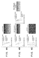
- FIG. 4A, 4B and 4C are schematic views showing correction according to the first embodiment of the present invention.
- FIG. 5 is a circuit diagram showing the arrangement of pixels arranged in the row and column directions according to the present invention.
- FIG. 6 is a view showing driving pulses in the moving image capturing mode according to the first embodiment of the present invention.
- the exposure times of any pixels from when accumulation of charges starts until the pixels are shielded from light can be equalized.
- the time until an operation of reading out the charges accumulated by exposure starts is different for each row. That is, the period (“accumulation time”), from when accumulation of charges by exposure starts until the accumulated charges are read out, on a row where the charges are read out last is longer (later) than that on a row where an operation of reading out the charges starts first.
- the present invention has been made in consideration of such problem, and provides an image capturing apparatus that corrects a decrease in image quality caused by noise occurring in image capturing signals when capturing an image by switching an image capturing operation by the electronic shutter to that by the mechanical shutter.
- a single-lens reflex digital camera according to the present invention will be described with reference to FIG. 1 .
- a single-lens reflex digital camera will be exemplified in this embodiment, the present invention is not limited to this.
- the present invention is also applicable to an image capturing apparatus having another arrangement as long as the image capturing apparatus has an arrangement which includes an image sensor for outputting image data as an electronic signal and controls the exposure time of the image sensor using a mechanical shutter as a light-shielding member.
- the digital camera includes an electronic shutter and mechanical shutter as shutters 203 , and includes, as image capturing modes, a moving image capturing mode using the electronic shutter and a still image capturing mode using the electronic shutter and the mechanical shutter.
- the mechanical shutter includes a blade unit corresponding to trailing blades used in the single-lens reflex camera.
- a shutter driving device 204 is a device for operating the shutters 203 , and includes a charge lever and control magnet.
- a unit pixel 101 of the image capturing apparatus will be explained.
- a photodiode (to be referred to as a PD hereinafter) 102 for converting light into charges accumulates charges.
- a transfer switch 103 transfers the charges generated in the PD to an FD (to be described later) by a transfer pulse pTX.
- a floating diffusion (to be referred to as an FD hereinafter) 104 temporarily accumulates the charges.
- An amplification MOS transistor 105 functions as a source follower.
- a selection switch 106 selects a pixel by a selection pulse pSELV.
- a reset switch 107 removes the charges accumulated in the FD 104 by a reset pulse pRES.
- the FD 104 , the amplification MOS transistor 105 , and a constant-current source 109 form a floating diffusion amplifier.
- Unit pixels having the above arrangement are arranged in the row and column directions. Each pixel is driven by peripheral circuits such as a horizontal scanning circuit 114 and vertical scanning circuit 112 for reading out a signal, and a signal is read out from the pixel. Charges in a pixel selected by the selection switch 106 are converted into a voltage, and output to a readout circuit 113 via a signal output line 108 .
- the constant-current source 109 serves as the load of the amplification MOS transistor 105 .
- a vertical scanning circuit 112 outputs a control signal for scanning pixels on each row by controlling the transfer switch 103 , selection switch 106 , and reset switch 107 .
- a selection switch 110 driven by a horizontal scanning circuit 114 selects an output signal from the readout circuit 113 .
- the transfer pulse pTX, reset pulse pRES, and selection pulse pSELV respective pulses on the nth scanning line (the nth line) scanned and selected by the vertical scanning circuit 112 are represented by pTXn, pRESn, and pSELVn.
- An image capturing operation will be performed as follows. On the nth line, during the time from a time t 41 to a time t 42 , the pulses pRESn and pTXn are applied to turn on the transfer switches 103 and reset switches 107 . A reset operation of removing unneeded charges accumulated in the PDs 102 and FDs 104 on the nth line is performed.
- the transfer switches 103 are turned off at the time t 42 , and an accumulation operation of accumulating photo-charges generated in the PDs starts.
- the pulse pTXn is applied to turn on the transfer switches 103 , and a transfer operation of transferring the photo-charges accumulated in the PDs 102 to the FDs 104 .
- the reset switches 107 need to be turned off before the transfer operation. In FIG. 6 , at the time t 42 , the reset switches 107 are turned off simultaneously with the transfer switches 103 .
- the time from the time t 42 to the time t 43 is an exposure time.
- the charges held in the FDs 104 are converted into voltages, and output to the readout circuit 113 as signals.
- the time from the start of the transfer operation at the time t 43 to the end of a readout operation at a time t 45 is a readout time on the nth line.
- the timing of a transfer operation on the (n+1)th line is adjusted to start immediately after the readout time on the nth line elapses.
- the time from the time t 41 at which the reset operation on the nth line starts to a time t 46 at which a reset operation on the (n+1)th line starts is a standby time on the (n+1)th line.
- the time from the start of a transfer operation to the end of a readout operation is a readout time
- the time from the start of a reset operation on a given line to the start of a reset operation on a next line is a standby time.
- the arrangement in which processing from a reset operation to a readout operation is performed for each pixel row at different timings will be referred to as the rolling shutter operation of the electronic shutter hereinafter.
- the start timing of accumulation of charges is different for each pixel row.
- the time required to accumulate charges by exposure can be constant in the image capturing apparatus.
- the exposure time of the image capturing apparatus is made constant by adjusting the timing of the reset operation to the traveling of the trailing blade unit.
- the exposure time of the image capturing apparatus is controlled by changing the time from the start of the reset operation until the light-shielding operation by the trailing blade unit.
- FIGS. 2A, 2B, 3A and 3B show the relationship between the timing of the reset operation and the timing of reading out signals after the light-shielding operation by the trailing blades in the still image capturing mode.
- FIGS. 2A, 2B, 3A and 3B show a case in which an image is captured by switching the image capturing mode from the moving image capturing mode by electronic shutter control using an electronic viewfinder to the still image capturing mode by mechanical shutter control.
- the mechanical shutter is open and the pixels are always irradiated with light.
- the reset operation of the pixels starts a charge accumulation operation.
- the reset operation is sequentially performed for the respective pixel rows at different timings in the moving image capturing mode after a time t 1 , as indicated by oblique lines in FIG. 2A . Signals are sequentially read out from the pixels on each row after the set exposure time elapses.
- the exposure time is constant in the moving image capturing mode by appropriately adjusting the start timing of the reset operation and the start timing of the readout operation. While the electronic shutter operates in the moving capturing mode, the mechanical shutter is released.
- the electronic shutter when capturing an image by the mechanical shutter by switching the mode from the moving image capturing mode to the still image capturing mode, the electronic shutter almost simultaneously resets the pixels at a timing coinciding with the traveling characteristic of the trailing blades.
- a time t 2 exposure starts, and a charge accumulation operation starts.
- the mechanical shutter At a time t 3 , the mechanical shutter almost simultaneously shields all the pixels from light.
- an operation of reading out signals from the pixels starts.
- the exposure time is controlled by appropriately adjusting the timing of the reset operation of the pixels by the electronic shutter and that of the light-shielding operation by the mechanical shutter.
- the accumulation time from when accumulation of charges by exposure starts until the accumulated charges are read out is equal to the time from the time t 2 to the time t 4 in the upper portion of the screen, and the time from the time t 2 to a time t 5 in the lower portion of the screen.
- the pixels on each row are equal in exposure time from the start of accumulation by the electronic shutter until the light-shielding operation by the mechanical shutter is performed, but are different in time until an operation of reading out the signals from the pixels on each row starts after the light-shielding operation.
- a uniform image is captured, a difference between the upper and lower portions of the shot image occurs due to the influence of noise, as shown in FIG. 4A .
- an operation of reading out the signals from the pixels is performed after the reset operation by the electronic shutter function starts exposure and the mechanical shutter performs a light-shielding operation. Therefore, the time until the signals are read out on each row is different. Due to a difference in accumulation time including the time from the start of exposure until the signals are read out from the pixels after the light-shielding operation, the luminance, dark current, and the like are different for each row. Consequently, as shown in FIG. 4A , noise such as shading may occur.
- the accumulation time on the nth row simply increases by t 5 ⁇ t 4 , as compared with the first row.
- noise charges such as a dark current generated by a pixel unit or the like after exposure and the like are accumulated in the photodiodes. Therefore, between the nth and first rows, a difference occurs in noise charges dependent on an accumulation time since the readout timings are different.
- an operation of reading out the charges from the pixels is separately performed so that the charges are read out first from the pixels on the subsequent even numbered rows, and then the charges are read out from the pixels on the subsequent odd numbered rows.
- the signals read out from the pixels are processed by a signal processing unit 206 , and corrected. Correction by the signal processing unit 206 will be explained. Processing from the time t 3 at which the mechanical shutter performs the light-shielding operation until the time t 4 at which the readout operation starts is common to the respective pixels, and is thus not considered.
- the signals obtained on the odd numbered rows during the period from the time t4a to a time t5 are as indicated by the shot image of the odd numbered rows in FIG. 4B , and are represented by expression (2) below.
- the difference between the signals on the adjacent rows can be assumed to be 0. That is, since each part of a1 ⁇ a0, . . . , a(2n+1) ⁇ a2n in the above expression (3) can be assumed to be 0, each bracketed part of expression (3) representing the difference between the signal of the pixel on the odd numbered row and that of the pixel on the even numbered row can be assumed to be nb.
- the difference in accumulation time between the 0th and first rows is (t 4 a ⁇ t 4 ), as shown in FIG. 2B .
- the signal processing unit 206 generates correction data for correcting noise based on the time difference (t 4 a ⁇ t 4 ) and the difference nb between the signal of the pixel on the odd numbered row and that of the pixel on the even numbered row, and corrects noise dependent on the accumulation time, thereby obtaining an output corrected image shown in FIG. 4C .
- a portion where the difference is obtained may be part of the image sensor.
- the difference in noise dependent on the accumulation time is larger. Thus, it is advantageous in detection.
- the differences may be obtained from all the even numbered rows and odd numbered rows.
- a region where the difference is obtained may be selected from a portion where a change in screen is small.
- Correction may be performed according to the readout time difference using, as the magnitude of noise dependent on the accumulation time, a value at the time of the last image capturing operation or a value obtained according to shooting conditions.
- the above-described processing of obtaining a correction value may be performed on an apparatus different from the camera with which shooting has been performed.
- n represents the number of rows of pixels arranged in a matrix and t represents the time taken to read out the charge accumulation amounts of all the pixels
- the time taken to read out the amounts on the nth row simply increases by t, as compared with the first row.
- noise charges such as a dark current generated by a pixel unit and the like are accumulated in photodiodes. Therefore, there is a difference in noise charges dependent on the readout time between the nth and first rows, in addition to the signal charges.
- a signal on the first row is represented by the sum (s1+t/n*a) of a signal s1 obtained by converting incident light from an object and noise t/n*a dependent on an accumulation time and corresponding to the accumulation time.
- a signal on the second row is represented by the sum (s2+2t/n*a) of a signal s2 and noise 2t/n*a dependent on an accumulation time and corresponding to the accumulation time.
- the pixels with the same color on the first and second rows whose accumulation times are different from each other undergo a subtraction operation, thereby obtaining (s2 ⁇ s1)+t/n*a.
- a signal obtained based on the difference between the pixels with the same color and noise dependent on an accumulation time are represented by expressions below.
- Noise dependent on an accumulation time obtained based on the difference between the pixels with the same color t/n*a, t/n*a, . . . , (n ⁇ (n ⁇ 1))*t/n*a (5)
- the above difference between the signals of the pixels with the same color on the adjacent rows for example, a signal obtained by s2 ⁇ s1 is approximately 0.
- a subtraction operation is performed for a plurality of sets of pixels with the same color and different accumulation times, thereby obtaining differences.
- noise dependent on an accumulation time for each set of signals between which the difference has been obtained is extracted. It is possible to appropriately correct the noise due to the accumulation time difference between the upper and lower pixels by obtaining correction data from the noise dependent on the accumulation time, and correcting noise dependent on the accumulation time difference t/n between the respective rows. Note that a case in which adjacent upper and lower pixels are not largely different in signal charges by the incident light from the object has been described in the above expressions.
- the above-described correction processing may be performed on an apparatus different from a camera with which shooting has been performed.
Landscapes
- Engineering & Computer Science (AREA)
- Multimedia (AREA)
- Signal Processing (AREA)
- Physics & Mathematics (AREA)
- General Physics & Mathematics (AREA)
- Studio Devices (AREA)
- Transforming Light Signals Into Electric Signals (AREA)
- Shutters For Cameras (AREA)
Abstract
Description
a0+b, a2+2b, a4+3b, . . . , a2n+nb (1)
a1+(n+1)b, a3+(n+2)b, . . . , a(2n+1)+2nb (2)
(a1+a0+nb)+(a3−a2+nb)+ . . . +(a(2n+1)−a2n+nb) (3)
s2−s1, s3−s2, . . . , sn−s(n−1) (4)
t/n*a, t/n*a, . . . , (n−(n−1))*t/n*a (5)
Claims (9)
Applications Claiming Priority (2)
| Application Number | Priority Date | Filing Date | Title |
|---|---|---|---|
| JP2013-238266 | 2013-11-18 | ||
| JP2013238266A JP2015099989A (en) | 2013-11-18 | 2013-11-18 | Imaging apparatus |
Publications (2)
| Publication Number | Publication Date |
|---|---|
| US20150138404A1 US20150138404A1 (en) | 2015-05-21 |
| US9398236B2 true US9398236B2 (en) | 2016-07-19 |
Family
ID=53172930
Family Applications (1)
| Application Number | Title | Priority Date | Filing Date |
|---|---|---|---|
| US14/519,464 Expired - Fee Related US9398236B2 (en) | 2013-11-18 | 2014-10-21 | Image capturing apparatus |
Country Status (2)
| Country | Link |
|---|---|
| US (1) | US9398236B2 (en) |
| JP (1) | JP2015099989A (en) |
Families Citing this family (2)
| Publication number | Priority date | Publication date | Assignee | Title |
|---|---|---|---|---|
| KR20160015712A (en) * | 2014-07-31 | 2016-02-15 | 삼성전자주식회사 | Apparatus and method for capturing images |
| AU2018329874A1 (en) | 2017-09-06 | 2020-03-12 | Baraja Pty Ltd | An optical beam director |
Citations (6)
| Publication number | Priority date | Publication date | Assignee | Title |
|---|---|---|---|---|
| JP2008022198A (en) | 2006-07-12 | 2008-01-31 | Canon Inc | Image sensing device |
| JP2008219523A (en) | 2007-03-05 | 2008-09-18 | Canon Inc | Imaging apparatus and control method thereof |
| US20080298791A1 (en) * | 2007-05-28 | 2008-12-04 | Canon Kabushiki Kaisha | Image pickup apparatus and lens apparatus |
| US20100188541A1 (en) * | 2009-01-28 | 2010-07-29 | Sony Corporation | Solid-state image capturing device, method of driving solid-state image capturing device, and image capturing apparatus |
| JP2011166397A (en) | 2010-02-09 | 2011-08-25 | Ricoh Co Ltd | Image pickup device and method for controlling the same |
| US20130206964A1 (en) | 2008-05-02 | 2013-08-15 | Canon Kabushiki Kaisha | Solid-state imaging apparatus with each pixel including a photoelectric conversion portion and plural holding portions |
-
2013
- 2013-11-18 JP JP2013238266A patent/JP2015099989A/en active Pending
-
2014
- 2014-10-21 US US14/519,464 patent/US9398236B2/en not_active Expired - Fee Related
Patent Citations (10)
| Publication number | Priority date | Publication date | Assignee | Title |
|---|---|---|---|---|
| JP2008022198A (en) | 2006-07-12 | 2008-01-31 | Canon Inc | Image sensing device |
| JP2008219523A (en) | 2007-03-05 | 2008-09-18 | Canon Inc | Imaging apparatus and control method thereof |
| US20080284873A1 (en) | 2007-03-05 | 2008-11-20 | Canon Kabushiki Kaisha | Image capture apparatus and control method thereof |
| US7920204B2 (en) | 2007-03-05 | 2011-04-05 | Canon Kabushiki Kaisha | Image capture apparatus and control method thereof |
| US20080298791A1 (en) * | 2007-05-28 | 2008-12-04 | Canon Kabushiki Kaisha | Image pickup apparatus and lens apparatus |
| US20130206964A1 (en) | 2008-05-02 | 2013-08-15 | Canon Kabushiki Kaisha | Solid-state imaging apparatus with each pixel including a photoelectric conversion portion and plural holding portions |
| US8625010B2 (en) | 2008-05-02 | 2014-01-07 | Canon Kabushiki Kaisha | Solid-state imaging apparatus with each pixel including a photoelectric converter portion and plural holding portions |
| US20100188541A1 (en) * | 2009-01-28 | 2010-07-29 | Sony Corporation | Solid-state image capturing device, method of driving solid-state image capturing device, and image capturing apparatus |
| JP2011166397A (en) | 2010-02-09 | 2011-08-25 | Ricoh Co Ltd | Image pickup device and method for controlling the same |
| US20120320231A1 (en) | 2010-02-09 | 2012-12-20 | Hiroshi Suito | Image capturing apparatus and method for controlling the same |
Also Published As
| Publication number | Publication date |
|---|---|
| JP2015099989A (en) | 2015-05-28 |
| US20150138404A1 (en) | 2015-05-21 |
Similar Documents
| Publication | Publication Date | Title |
|---|---|---|
| US20200351464A1 (en) | Image sensor | |
| US10205904B2 (en) | Image sensor capable of correcting noise caused by dark charge of a floating diffusion portion, control method therefor, and image capturing apparatus | |
| KR101435964B1 (en) | Imaging device and driving method for solid-state image sensor | |
| US8174590B2 (en) | Image pickup apparatus and image pickup method | |
| US9930279B2 (en) | Image capturing apparatus and control method thereof, and storage medium | |
| JP5455798B2 (en) | Image processing device | |
| JP5128889B2 (en) | Solid-state imaging device and solid-state imaging system using the same | |
| US10397502B2 (en) | Method and apparatus for imaging an object | |
| US10511791B2 (en) | Image capturing apparatus capable of performing readout from a plurality of divided areas of a pixel area and control method therefor | |
| JP5959834B2 (en) | Imaging device | |
| US20160344962A1 (en) | Image processing apparatus, image processing method, and image capturing apparatus | |
| JP2014060573A (en) | Solid-state image sensor, control method and electronic apparatus | |
| CN101753843A (en) | Image sensing apparatus and control method therefor | |
| US8305472B2 (en) | Image capturing system | |
| JP2007074435A (en) | Solid-state imaging device and its drive method | |
| US10594968B2 (en) | Image sensor and imaging apparatus | |
| US9398236B2 (en) | Image capturing apparatus | |
| JP2018082295A (en) | Imaging device and imaging system | |
| US9813646B2 (en) | Solid-state imaging apparatus, imaging system, and method for driving solid-state imaging apparatus, where longer accumulation time is used for light-shielded pixels | |
| US11252354B2 (en) | Image sensor, control method thereof, and image capturing apparatus | |
| JP2008067060A (en) | Imaging apparatus | |
| JP7277251B2 (en) | Imaging device and its control method | |
| JP5311943B2 (en) | Imaging apparatus, control method, and program | |
| JP2016029756A (en) | Imaging device | |
| JP2015035723A (en) | Imaging device |
Legal Events
| Date | Code | Title | Description |
|---|---|---|---|
| AS | Assignment |
Owner name: CANON KABUSHIKI KAISHA, JAPAN Free format text: ASSIGNMENT OF ASSIGNORS INTEREST;ASSIGNORS:JOHNSON, MICHIKO;KOBAYASHI, MASAHIRO;ITOH, HIDEYUKI;AND OTHERS;REEL/FRAME:035623/0327 Effective date: 20141017 |
|
| STCF | Information on status: patent grant |
Free format text: PATENTED CASE |
|
| MAFP | Maintenance fee payment |
Free format text: PAYMENT OF MAINTENANCE FEE, 4TH YEAR, LARGE ENTITY (ORIGINAL EVENT CODE: M1551); ENTITY STATUS OF PATENT OWNER: LARGE ENTITY Year of fee payment: 4 |
|
| FEPP | Fee payment procedure |
Free format text: MAINTENANCE FEE REMINDER MAILED (ORIGINAL EVENT CODE: REM.); ENTITY STATUS OF PATENT OWNER: LARGE ENTITY |
|
| LAPS | Lapse for failure to pay maintenance fees |
Free format text: PATENT EXPIRED FOR FAILURE TO PAY MAINTENANCE FEES (ORIGINAL EVENT CODE: EXP.); ENTITY STATUS OF PATENT OWNER: LARGE ENTITY |
|
| STCH | Information on status: patent discontinuation |
Free format text: PATENT EXPIRED DUE TO NONPAYMENT OF MAINTENANCE FEES UNDER 37 CFR 1.362 |
|
| FP | Lapsed due to failure to pay maintenance fee |
Effective date: 20240719 |