US8604350B2 - Multilayer wiring substrate and manufacturing method of multilayer wiring substrate - Google Patents
Multilayer wiring substrate and manufacturing method of multilayer wiring substrate Download PDFInfo
- Publication number
- US8604350B2 US8604350B2 US13/143,490 US201113143490A US8604350B2 US 8604350 B2 US8604350 B2 US 8604350B2 US 201113143490 A US201113143490 A US 201113143490A US 8604350 B2 US8604350 B2 US 8604350B2
- Authority
- US
- United States
- Prior art keywords
- particles
- wiring board
- multilayer wiring
- metal regions
- metal
- Prior art date
- Legal status (The legal status is an assumption and is not a legal conclusion. Google has not performed a legal analysis and makes no representation as to the accuracy of the status listed.)
- Expired - Fee Related
Links
Images


Classifications
-
- H—ELECTRICITY
- H05—ELECTRIC TECHNIQUES NOT OTHERWISE PROVIDED FOR
- H05K—PRINTED CIRCUITS; CASINGS OR CONSTRUCTIONAL DETAILS OF ELECTRIC APPARATUS; MANUFACTURE OF ASSEMBLAGES OF ELECTRICAL COMPONENTS
- H05K3/00—Apparatus or processes for manufacturing printed circuits
- H05K3/40—Forming printed elements for providing electric connections to or between printed circuits
- H05K3/4038—Through-connections; Vertical interconnect access [VIA] connections
- H05K3/4053—Through-connections; Vertical interconnect access [VIA] connections by thick-film techniques
- H05K3/4069—Through-connections; Vertical interconnect access [VIA] connections by thick-film techniques for via connections in organic insulating substrates
-
- H—ELECTRICITY
- H05—ELECTRIC TECHNIQUES NOT OTHERWISE PROVIDED FOR
- H05K—PRINTED CIRCUITS; CASINGS OR CONSTRUCTIONAL DETAILS OF ELECTRIC APPARATUS; MANUFACTURE OF ASSEMBLAGES OF ELECTRICAL COMPONENTS
- H05K2201/00—Indexing scheme relating to printed circuits covered by H05K1/00
- H05K2201/01—Dielectrics
- H05K2201/0183—Dielectric layers
- H05K2201/0195—Dielectric or adhesive layers comprising a plurality of layers, e.g. in a multilayer structure
-
- H—ELECTRICITY
- H05—ELECTRIC TECHNIQUES NOT OTHERWISE PROVIDED FOR
- H05K—PRINTED CIRCUITS; CASINGS OR CONSTRUCTIONAL DETAILS OF ELECTRIC APPARATUS; MANUFACTURE OF ASSEMBLAGES OF ELECTRICAL COMPONENTS
- H05K2201/00—Indexing scheme relating to printed circuits covered by H05K1/00
- H05K2201/02—Fillers; Particles; Fibers; Reinforcement materials
- H05K2201/0203—Fillers and particles
- H05K2201/0263—Details about a collection of particles
- H05K2201/0272—Mixed conductive particles, i.e. using different conductive particles, e.g. differing in shape
-
- H—ELECTRICITY
- H05—ELECTRIC TECHNIQUES NOT OTHERWISE PROVIDED FOR
- H05K—PRINTED CIRCUITS; CASINGS OR CONSTRUCTIONAL DETAILS OF ELECTRIC APPARATUS; MANUFACTURE OF ASSEMBLAGES OF ELECTRICAL COMPONENTS
- H05K2203/00—Indexing scheme relating to apparatus or processes for manufacturing printed circuits covered by H05K3/00
- H05K2203/04—Soldering or other types of metallurgic bonding
- H05K2203/0425—Solder powder or solder coated metal powder
-
- H—ELECTRICITY
- H05—ELECTRIC TECHNIQUES NOT OTHERWISE PROVIDED FOR
- H05K—PRINTED CIRCUITS; CASINGS OR CONSTRUCTIONAL DETAILS OF ELECTRIC APPARATUS; MANUFACTURE OF ASSEMBLAGES OF ELECTRICAL COMPONENTS
- H05K3/00—Apparatus or processes for manufacturing printed circuits
- H05K3/46—Manufacturing multilayer circuits
- H05K3/4611—Manufacturing multilayer circuits by laminating two or more circuit boards
- H05K3/4623—Manufacturing multilayer circuits by laminating two or more circuit boards the circuit boards having internal via connections between two or more circuit layers before lamination, e.g. double-sided circuit boards
-
- H—ELECTRICITY
- H05—ELECTRIC TECHNIQUES NOT OTHERWISE PROVIDED FOR
- H05K—PRINTED CIRCUITS; CASINGS OR CONSTRUCTIONAL DETAILS OF ELECTRIC APPARATUS; MANUFACTURE OF ASSEMBLAGES OF ELECTRICAL COMPONENTS
- H05K3/00—Apparatus or processes for manufacturing printed circuits
- H05K3/46—Manufacturing multilayer circuits
- H05K3/4611—Manufacturing multilayer circuits by laminating two or more circuit boards
- H05K3/4626—Manufacturing multilayer circuits by laminating two or more circuit boards characterised by the insulating layers or materials
-
- Y—GENERAL TAGGING OF NEW TECHNOLOGICAL DEVELOPMENTS; GENERAL TAGGING OF CROSS-SECTIONAL TECHNOLOGIES SPANNING OVER SEVERAL SECTIONS OF THE IPC; TECHNICAL SUBJECTS COVERED BY FORMER USPC CROSS-REFERENCE ART COLLECTIONS [XRACs] AND DIGESTS
- Y10—TECHNICAL SUBJECTS COVERED BY FORMER USPC
- Y10T—TECHNICAL SUBJECTS COVERED BY FORMER US CLASSIFICATION
- Y10T29/00—Metal working
- Y10T29/49—Method of mechanical manufacture
- Y10T29/49002—Electrical device making
- Y10T29/49117—Conductor or circuit manufacturing
- Y10T29/49124—On flat or curved insulated base, e.g., printed circuit, etc.
- Y10T29/49155—Manufacturing circuit on or in base
- Y10T29/49165—Manufacturing circuit on or in base by forming conductive walled aperture in base
- Y10T29/49167—Manufacturing circuit on or in base by forming conductive walled aperture in base with deforming of conductive path
Definitions
- the present invention relates to a multilayer wiring board with via-hole conductors for interlayer connection between two wirings three-dimensionally formed on an insulating resin layer. More specifically, it relates to improvements in via-hole conductors for interlayer connection between wirings in multiple layers.
- Patent Document 1 discloses a via-hole conductor having a matrix-domain structure in which a plurality of domains made of Cu particles are dotted in a CuSn compound matrix.
- Patent Document 2 discloses a sinterable composition for use in via-hole conductor formation, which includes a high-melting-point particle-phase material that includes Cu, and a low-melting-point material that is a selected metal such as tin (Sn) or a tin alloy.
- a sinterable composition is a composition sinterable in the presence of a liquid phase or a transient liquid phase.
- Patent Document 3 discloses a via-hole conductor material in which alloy layers with a solidus temperature of 250° C. or higher are formed on circumferences of copper particles by heating conductive paste, which contains tin-bismuth (Sn—Bi) metallic particles and the copper particles, to a temperature greater than or equal to the melting point of the Sn—Bi metallic particles.
- conductive paste which contains tin-bismuth (Sn—Bi) metallic particles and the copper particles
- Patent Document 4 discloses a multilayer wiring board provided with via-hole conductors which contain copper and tin in a total amount of 80 to 97% by weight, along with bismuth in a proportion of 3 to 20% by weight.
- FIG. 21 is a schematic cross-sectional view of a connection between a wiring 1 and a via-hole conductor 2 in the multilayer wiring board disclosed in Patent Document 1.
- the via-hole conductor 2 is in contact with the wiring 1 formed on the surface of the multilayer wiring board.
- the via-hole conductor 2 includes a matrix, which includes an intermetallic compound 4 such as Cu 3 Sn or Cu 6 Sn 5 , and copper-containing powder 3 dotted as domains in the matrix including the intermetallic compound 4 .
- a matrix-domain structure is formed by setting the weight ratio represented as Sn/(Cu+Sn) within the range from 0.25 to 0.75.
- the via-hole conductor 2 as such has a problem where voids and cracks ( 5 in FIG. 21 ) tend to occur under thermal shock testing.
- such voids and cracks are openings caused by Cu diffusion among the Sn—Bi metallic particles to generate a CuSn compound such as Cu 3 Sn or Cu 6 Sn 5 .
- such voids are also caused by Cu 3 Sn, which is an intermetallic compound of Cu and Sn contained in a Cu—Sn diffusion joint formed at a Cu—Sn interface, being heated under any of various reliability tests and turning into Cu 6 Sn 5 to generate internal stress inside the via-hole conductor 2 .
- the sinterable composition disclosed in Patent Document 2 is a composition which is generated, for example, during hot pressing for prepreg lamination and sintered in the presence or absence of a transient liquid phase.
- a sinterable composition includes Cu, Sn, and lead (Pb) and therefore is difficult to be rendered Pb-free as demanded by the market.
- Pb lead
- such a sinterable composition reaches a high temperature in the range from 180° C. to 325° C. at the time of hot pressing and therefore is difficult to apply as a standard insulating resin layer (which may also be called a glass epoxy resin layer) to be obtained by impregnating glass fibers with epoxy resin.
- the via-hole conductor material disclosed in Patent Document 3 has alloy layers with high resistance formed on surface layers of Cu particles. Accordingly, there is a problem of higher resistance when compared with connection resistance resulting only from contact between Cu particles and between Ag particles as in general conductive paste which contains Cu particles, silver (Ag) powder, etc.
- the via-hole conductor disclosed in Patent Document 4 also has alloy layers with high resistance formed on surface layers of Cu particles and therefore has the problem of not being able to achieve interlayer connection with sufficiently low resistance, as will be described later.
- An objective of the present invention is to provide a multilayer wiring board capable of meeting the need for being Pb-free, in which interlayer connections are achieved by low-resistance via-hole conductors with high connection reliability.
- One aspect of the present invention is directed to a multilayer wiring board comprising at least one insulating resin layer, a first wiring laid on a first surface of the insulating resin layer, a second wiring laid on a second surface of the insulating resin layer, and a via hole conductor provided so as to pierce the insulating resin layer for electrically connecting the first wiring and the second wiring, wherein the via-hole conductor includes metal and resin portions, the metal portion includes first metal regions including a joined unit made of copper particles for forming a path electrically connecting the first wiring and the second wiring, second metal regions mainly composed of at least one metal selected from the group consisting of tin, a tin-copper alloy, and a tin-copper intermetallic compound, and third metal regions mainly composed of bismuth and in contact with the second metal regions, the copper particles forming the joined unit are in plane contact with one another to form plane contact portions, and the second metal regions at least partially are in contact with the first metal regions.
- another aspect of the present invention is directed to a multilayer wiring board manufacturing method comprising a first step of covering surfaces of an insulating resin sheet with protective films, a second step of forming a through-hole by perforating the insulating resin sheet via either of the protective films, a third step of filling the through-hole with via paste, the via paste including copper particles, tin-bismuth based solder particles, and thermally curable resin, a fourth step of removing the protective films after the third step, thereby revealing protrusions formed by the via paste partially projecting from the through-hole, a fifth step of placing metal foil on at least one surface of the insulating resin sheet so as to cover the protrusions, a sixth step of subjecting the metal foil to compression bonding onto the surface of the insulating resin sheet to compress the via paste by way of the protrusions at a temperature lower than the melting point of the tin-bismuth based solder particles, thereby forming first metal regions including joined units made of the copper particles, the
- the present invention makes it possible to achieve interlayer connection with low resistance by forming a low-resistance conduction path using a joined unit made of copper particles and having plane contact portions formed by copper particles contained in via-hole conductors of a multilayer wiring board, which are in plane contact with one another.
- the joined unit made of copper particles is reinforced by second metal regions contacting at least part of the joined unit made of copper particles, in which the second metal regions are mainly composed of at least one metal harder than the copper particles and selected from the group consisting of tin, a tin-copper alloy, and a tin-copper intermetallic compound.
- FIG. 1A is a schematic cross-sectional view of a multilayer wiring board 11 in a first embodiment.
- FIG. 1B is an enlarged schematic cross-sectional view around a via-hole conductor 14 in FIG. 1A .
- FIG. 2 is an explanatory diagram describing a copper-particle joined unit 17 a in the first embodiment, which is formed by a number of Cu particles 7 in plane contact with one another and functions as a conduction path 23 between wirings 12 .
- FIG. 3 is a schematic cross-sectional view describing a via-hole conductor where Cu/Sn is less than 1.59.
- FIG. 4A illustrates a schematic cross-sectional view describing a step in a method for manufacturing a multilayer wiring board 11 in the first embodiment.
- FIG. 4B illustrates a schematic cross-sectional view describing a step subsequent to the step of FIG. 4A in the method for manufacturing the multilayer wiring board 11 .
- FIG. 4C illustrates a schematic cross-sectional view describing a step subsequent to the step of FIG. 4B in the method for manufacturing the multilayer wiring board 11 .
- FIG. 4D illustrates a schematic cross-sectional view describing a step subsequent to the step of FIG. 4C in the method for manufacturing the multilayer wiring board 11 .
- FIG. 5A illustrates a schematic cross-sectional view describing a step subsequent to the step of FIG. 4D in the method for manufacturing the multilayer wiring board 11 .
- FIG. 5B illustrates a schematic cross-sectional view describing a step subsequent to the step of FIG. 5A in the method for manufacturing the multilayer wiring board 11 .
- FIG. 5C illustrates a schematic cross-sectional view describing a step subsequent to the step of FIG. 5B in the method for manufacturing the multilayer wiring board 11 .
- FIG. 6A illustrates a schematic cross-sectional view describing a step in multilayering of a wiring board.
- FIG. 6B illustrates a schematic cross-sectional view describing a step subsequent to the step of FIG. 6A in multilayering of the wiring board.
- FIG. 6C illustrates a schematic cross-sectional view describing a step subsequent to the step of FIG. 6B in multilayering of the wiring board.
- FIG. 7A is a schematic cross-sectional view illustrating a portion around one through-hole 27 in a resin sheet 25 , which is filled with via paste 28 , in the first embodiment.
- FIG. 7B is a schematic cross-sectional view illustrating a state where the via paste 28 applied in the through-hole 27 of FIG. 7A is compressed in the embodiment.
- FIG. 8A is a schematic cross-sectional view of a multilayer wiring board 111 in a second embodiment.
- FIG. 8B is an enlarged schematic cross-sectional view around one via-hole conductor 14 in FIG. 8A .
- FIG. 9A illustrates a schematic cross-sectional view describing a step in a method for manufacturing a multilayer wiring board 111 in the second embodiment.
- FIG. 9B illustrates a schematic cross-sectional view describing a step subsequent to the step of FIG. 9A in the method for manufacturing the multilayer wiring board 111 .
- FIG. 9C illustrates a schematic cross-sectional view describing a step subsequent to the step of FIG. 9B in the method for manufacturing the multilayer wiring board 111 .
- FIG. 9D illustrates a schematic cross-sectional view describing a step subsequent to the step of FIG. 9C in the method for manufacturing the multilayer wiring board 111 .
- FIG. 10A illustrates a schematic cross-sectional view describing a step subsequent to the step of FIG. 9D in the method for manufacturing the multilayer wiring board 111 .
- FIG. 10B illustrates a schematic cross-sectional view describing a step subsequent to the step of FIG. 10A in the method for manufacturing the multilayer wiring board 111 .
- FIG. 10C illustrates a schematic cross-sectional view describing a step subsequent to the step of FIG. 10B in the method for manufacturing the multilayer wiring board 111 .
- FIG. 11A illustrates a schematic cross-sectional view describing a step in multilayering of a wiring board.
- FIG. 11B illustrates a schematic cross-sectional view describing a step subsequent to the step of FIG. 11A in multilayering of the wiring board.
- FIG. 11C illustrates a schematic cross-sectional view describing a step subsequent to the step of FIG. 11B in multilayering of the wiring board.
- FIG. 12A is a schematic cross-sectional view illustrating a portion around one through-hole 27 in a prepreg 125 , which is filled with via paste 28 in the second embodiment.
- FIG. 12B is a schematic cross-sectional view illustrating a state where the via paste 28 applied in the through-hole of FIG. 12A is compressed in the second embodiment.
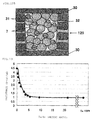
- FIG. 13 is a graph showing resistance values (1 via/m ⁇ ) versus the weight ratio Cu/Sn in via-hole conductors obtained by way of example.
- FIG. 14A shows a cross-sectional scanning electron microscope (SEM) photograph of a via conductor of a multilayer wiring board obtained by way of example at 3000-times magnification.
- FIG. 14B shows a tracing of the SEM photograph of FIG. 14A .
- FIG. 15A shows a cross-sectional SEM photograph of the via conductor of the multilayer wiring board obtained by way of example at 6000-times magnification.
- FIG. 15B shows a tracing of the SEM photograph of FIG. 15A .
- FIG. 16A shows a cross-sectional SEM photograph of the via conductor of the multilayer wiring board obtained by way of example.
- FIG. 16B shows a tracing of the SEM photograph of FIG. 16A .
- FIG. 17A shows an image obtained by Cu-element mapping from the EPMA image of FIG. 16A .
- FIG. 17B shows a tracing of the mapping image of FIG. 17A .
- FIG. 18A shows an image obtained by Sn-element mapping from the EPMA image of FIG. 16A .
- FIG. 18B shows a tracing of the mapping image of FIG. 18A .
- FIG. 19A shows an image obtained by Bi-element mapping from the EPMA image of FIG. 16A .
- FIG. 19B shows a tracing of the mapping image of FIG. 19A .
- FIG. 20 is a graph comparing resistance between conventionally known via-hole conductors obtained from conductive paste of Patent Document 4 and a via-hole conductor according to the invention of the present application.
- FIG. 21 is a schematic cross-sectional view describing a cross section of a conventional via-hole conductor.
- FIG. 1A is a schematic cross-sectional view of a multilayer wiring board 11 of the present embodiment. Also, FIG. 1B is an enlarged schematic cross-sectional view around a via-hole conductor 14 in the multilayer wiring board 11 of FIG. 1A .
- via-hole conductors 14 piercing through insulating resin layers 13 provide electrical interlayer connections between a plurality of wirings 12 , which are made of metal foil such as copper foil and three-dimensionally formed on the insulating resin layers 13 .
- FIG. 1B is an enlarged schematic cross-sectional view around one via-hole conductor 14 .
- “ 12 ( 12 a , 12 b )” denotes the wirings
- “ 13 ” denotes the insulating resin layer
- “ 14 ” denotes the via-hole conductor.
- the via-hole conductor 14 includes a metal portion 15 and a resin portion 16 .
- the insulating resin layer 13 is made of a laminated heat-resistant resin sheet in which cured resin layers 13 b are laminated on opposite surfaces of a heat-resistant resin sheet 13 a .
- the metal portion 15 includes first metal regions 17 formed of Cu particles 7 , second metal regions 18 mainly composed of at least one metal selected from the group consisting of tin, a tin-copper alloy, and a tin-copper intermetallic compound, and third metal regions 19 mainly composed of Bi. At least part of the Cu particles 7 are brought into contact and joined together by plane contact portions 20 in which they are in direct plane contact with one another, thereby forming a copper-particle joined unit 17 a in a portion denoted by broken lines. Furthermore, the joined unit 17 a functions as a low-resistance conduction path for electrically connecting the upper-layer wiring 12 a and the lower-layer wiring 12 b.
- the Cu particles 7 have an average particle diameter in the range preferably from 0.1 to 20 ⁇ m, more preferably from 1 to 10 ⁇ m.
- the average particle diameter of the Cu particles 7 is excessively small, the number of contact points in the via-hole conductors 14 tends to increase, resulting in higher conduction resistance. Furthermore, particles with such a particle diameter tend to be expensive.
- the average particle diameter of the Cu particles 7 is excessively large, it is unlikely to be possible to achieve an increased filling rate when the via-hole conductors 14 are formed with smaller diameters such as from 100 to 150 ⁇ m.
- the purity of the Cu particles 7 is preferably 90% by mass or more, more preferably 99% by mass or more.
- the Cu particles 7 become softer as the copper purity thereof increases. As a result, they become more easy to deforming in a pressurization step to be described later, and therefore when a plurality of Cu particles 7 are brought into contact with one another, the Cu particles 7 are readily deformed, resulting in increased contact areas of the Cu particles 7 .
- high purity is preferable from the viewpoint of resistance reduction of the Cu particles 7 .
- the average particle diameter of the Cu particles 7 and the plane contact portions 20 in which the Cu particles 7 are in plane contact with one another are measured and confirmed using a scanning electron microscope (SEM) to observe a sample created by embedding a formed multilayer wiring board in resin and thereafter polishing cross sections of via-hole conductors 14 (using microfabrication means, such as focused ion beam, as necessary).
- SEM scanning electron microscope
- a number of Cu particles 7 are brought into contact with one another to form a joined unit 17 a , thereby forming a low-resistance conduction path between the wirings 12 a and 12 b .
- a joined unit 17 a By forming such a joined unit 17 a , it becomes possible to reduce connection resistance between the wirings 12 a and 12 b.
- the low-resistance joined units 17 a be formed with a complicated network of a number of Cu particles 7 in random contact as shown in FIG. 1B , rather than in orderly arrangement.
- the joined units 17 a each forming such a network make it possible to increase the reliability of electric connections.
- a number of Cu particles 7 are preferably in plane contact with one another in random positions. By setting the Cu particles 7 in plane contact with one another in random positions, it becomes possible to allow deformation to disperse stress caused within the via-hole conductors 14 when heated and externally applied force.
- the volume percent of the Cu particles 7 contained in the via-hole conductors 14 is preferably 30 to 90% by volume, more preferably 40 to 70% by volume.
- the volume percent of the Cu particles 7 is excessively low, the electrical connection reliability of the joined units 17 a formed as conduction paths by a number of Cu particles 7 in plane contact with one another tends to decrease, and when the volume percent is excessively high, resistance values tend to cause fluctuations in a reliability test.
- the second metal regions 18 mainly composed of at least one metal selected from the group consisting of tin, a tin-copper alloy, and a tin-copper intermetallic compound are formed so as to be in contact with the surfaces of the first metal regions 17 .
- the first metal regions 17 are reinforced by forming the second metal regions 18 on the surfaces of the first metal regions 17 in such a manner.
- the second metal regions 18 at least partially cover and extend over the plane contact portions 20 in which the copper particles 7 are in plane contact with one another.
- the contact state of the plane contact portions 20 is further strengthened by forming the second metal regions 18 extending over the plane contact portions 20 in such a manner.
- the second metal regions 18 are mainly composed of at least one metal selected from the group consisting of tin, a tin-copper alloy, and a tin-copper intermetallic compound. Concretely, for example, they are mainly composed of a metal including a simple substance of Sn, or Cu 6 Sn 5 , Cu 3 Sn or the like. In addition, other metal elements such as Bi and Cu may be included as the remaining components in such a range as not to ruin the effect of the present invention, concretely, in the range of, for example, 10% by mass or less.
- the third metal regions 19 mainly composed of Bi are preferably in contact with the second metal regions 18 but out of contact with the Cu particles 7 , as shown in FIG. 1B .
- the third metal regions 19 do not reduce the conductivity of the first metal regions 17 so long as the third metal regions 19 are present so as not to be in contact with the Cu particles 7 .
- the third metal regions 19 are mainly composed of Bi.
- the third metal regions 19 may include, for example, an alloy or intermetallic compound of Bi and Sn as the remaining component in such a range as not to ruin the effect of the present invention, concretely, in the range of, for example, 20% by mass or less.
- the second metal regions 18 and the third metal regions 19 are in contact with each other, they normally include both Bi and Sn.
- the second metal regions 18 have a higher Sn concentration than the third metal regions 19
- the third metal regions 19 have a higher Bi concentration than the second metal regions 18 .
- the metal portions 15 thus included in the via-hole conductors 14 include the first metal regions 17 made of copper particles 7 , the second metal regions 18 mainly composed of at least one metal selected from the group consisting of tin, a tin-copper alloy, and a tin-copper intermetallic compound, and the third metal regions 19 mainly composed of bismuth.
- the weight ratio of Cu to Sn (Cu/Sn) in the metal portions 15 is preferably in the range from 1.59 to 21.43. The meaning of the Cu/Sn ratio will be described in detail later.
- the resin portions 16 included in the via-hole conductors 14 are made of a hardened material of curable resin.
- the curable resin is not specifically limited, but concretely, for example, hardened epoxy resin is particularly preferred in view of its superior heat resistance and low linear expansion coefficient.
- the volume percent of the resin portions 16 in the via-hole conductors 14 is preferably 0.1 to 50% by volume, more preferably, 0.5 to 40% by volume.
- the volume percent of the resin portions 16 is excessively high, resistance values tend to increase, and when the volume percent is excessively low, conductive paste preparation at the time of manufacture tends to be difficult.
- FIG. 2 is an explanatory diagram for description focusing on a conduction path 23 of one joined unit 17 a formed by a number of Cu particles 7 in contact with one another. Also, for the sake of convenience, elements including the resin portion 16 are not shown. Furthermore, “ 21 ” denotes a virtual spring conveniently shown for describing the effect of the via-hole conductor 14 .
- the joined unit 17 a formed by a number of Cu particles 7 in random plane contact with one another functions as the conduction path 23 for electrical interlayer connection between the wirings 12 a and 12 b .
- the second metal regions 18 are preferably formed so as to cover around and extend over the plane contact portions 20 .
- Such outward force is weakened through deformation of the Cu particles 7 , which are highly flexible, elastic deformation of the joined units 17 a formed by the Cu particles 7 in contact with one another, or slight shift in contact positions of the Cu particles 7 .
- the second metal regions 18 are inclined to resist deformation of the joined units 17 a , particularly, deformation of the plane contact portions 20 . Accordingly, in the case where the joined units 17 a keep on deforming indefinitely, the second metal regions 18 regulate the deformation to some extent, and therefore the deformation does not progress to such an extent that the plane contact portions 20 between the Cu particles 7 become out of contact.
- the joined units 17 a formed by the Cu particles 7 in contact with one another are likened to springs, when a certain amount of force is applied to the joined units 17 a , the joined units 17 a keep on deforming to some extent as if the springs were expanding, and when the joined units 17 a further keep on deforming, the harder second metal regions 18 regulate the deformation.
- a similar effect is also achieved when inward force as indicated by arrows 22 b is applied to the multilayer wiring board 11 . In this manner, as if the joined units 17 a were the springs 21 , deformation of the joined units 17 a is regulated against forces in any directions whether they are external or internal, thereby ensuring the reliability of electrical connection.
- protective films 26 are attached to opposite surfaces of a resin sheet 25 , as shown in FIG. 4A .
- the resin sheet 25 used in the present embodiment is a laminate of uncured resin layers 25 a put on opposite surfaces of a heat-resistant resin sheet 13 a .
- an insulating resin layer with sufficient insulation properties can be formed even if its thickness is, for example, 15 ⁇ m or less or even 6 ⁇ m or less.
- the uncured resin layers 25 a adhere metal foil and formed wirings.
- any resin sheet can be used as the heat-resistant resin sheet 13 a without limitation so long as it can resist the temperature of soldering.
- Specific examples thereof include sheets made of, for example, polyimide, liquid crystal polymer, polyester ether ketone, or the like. Among them, the polyimide sheet is particularly preferable.
- the heat-resistant resin sheet 13 a has a thickness of, preferably, 1 to 100 ⁇ m, more preferably, 3 to 75 ⁇ m, particularly preferably, 7.5 to 60 ⁇ m.
- the uncured resin layers 25 a are, for example, uncured adhesive layers made of epoxy resin or suchlike.
- each of the uncured resin layers 25 a has a thickness of, preferably, 1 to 30 ⁇ m, more preferably, 5 to 10 ⁇ m, in view of contribution to thickness reduction of the multilayer wiring board.
- Various resin films can be used as protective films. Specific examples thereof include resin films of PET (polyethylene terephthalate), PEN (polyethylene naphthalate), or the like. Such a resin film has a thickness of, preferably, 0.5 to 50 ⁇ m, more preferably, 1 to 30 ⁇ m. In the case of such a thickness, sufficiently high protrusions made from via paste can be revealed by removing protective films, as will be described later.
- One example of the method for attaching the protective films 26 to the resin sheet 25 is direct attachment taking advantage of surface tackiness of the surfaces of the uncured resin layers 25 a.
- the resin sheet 25 with the protective films 26 disposed thereon is perforated from outside either of the protective films 26 , thereby making through-holes 27 , as shown in FIG. 4B .
- Various methods can be used for the perforation, including noncontact processing methods using a carbon dioxide gas laser, a YAG laser, or the like, and other methods using drilling or suchlike.
- the through-holes have a diameter of, for example, 10 to 500 ⁇ m, or even about 50 to 300 ⁇ m.
- via paste 28 is applied to completely fill the through-holes 27 , as shown in FIG. 4C .
- the via paste 28 contains Cu particles, Sn—Bi based solder particles containing Sn and Bi, and a curable resin component such as epoxy resin.
- the average particle diameter of the Cu particles is in the range of, preferably, from 0.1 to 20 ⁇ m, more preferably, from 1 to 10 ⁇ m.
- the average particle diameter of the Cu particles is excessively small, a high degree of filling in the through-holes 27 tends to be difficult and also expensive.
- filling tends to be difficult when forming via-hole conductors with smaller diameters.
- the Cu particles are not specifically limited to any particle form.
- examples of the form include spherical, flat, polygonal, scaly, flaky forms, and other forms with surface projections.
- the particles may be primary particles, or secondary particles may be formed.
- the Sn—Bi based solder particles are not limited to any specific particulate solder so long as Sn and Bi are contained.
- the Sn—Bi based solder particles have its eutectic point changeable in the range from about 138° C. to 232° C. by changing its composition ratio or by adding various elements.
- indium (In), silver (Ag), zinc (Zn) or the like may be added to improve wettability, flowability, etc.
- Particularly preferable among them is, for example, Sn-58Bi solder, which is environmentally-friendly lead-free solder with a low eutectic point of 138° C.
- the average particle diameter of the Sn—Bi based solder particles are in the range of, preferably, from 0.1 to more preferably, from 2 to 15 ⁇ m.
- An excessively small average particle diameter of the Sn—Bi based solder particles increases the specific surface area, resulting in an increased proportion of an oxide film on the surface, which leads to the tendency to be resistant to melting.
- an excessively large average particle diameter of the Sn—Bi based solder particles lead to the tendency to reduce via-hole fillability.
- epoxy resin which is a preferred curable resin component
- epoxy resin include glycidyl ether epoxy resin, alycyclic epoxy resin, glycidyl amine epoxy resin, glycidyl ester epoxy resin, and other modified epoxy resin.
- a curing agent may be combined with epoxy resin. While the curing agent is not limited to any specific type, it is preferable to use a curing agent which contains an amine compound having at least one or more hydroxyl groups in its molecules. Such a curing agent is preferable in that it functions as a curing catalyst for epoxy resin, and has a function of reducing oxide films present on the surfaces of the Cu particles and the Sn—Bi based solder particles, thereby lessening contact resistance at the time of junction.
- the amine compound which has a boiling point higher than the melting point of the Sn—Bi based solder particles, is particularly preferable in that it is particularly highly effective in lessening the contact resistance at the time of junction.
- Such an amine compound examples include 2-methylaminoethanol (boiling point: 160° C.), N,N-diethyl ethanolamine (boiling point: 162° C.), N,N-dibutylethanolamine (boiling point: 229° C.), N-methylethanolamine (boiling point: 160° C.), N-methyldiethanolamine (boiling point: 247° C.), N-ethylethanolamine (boiling point: 169° C.), N-butylethanolamine (boiling point: 195° C.), diisopropanolamine (boiling point: 249° C.), N,N-diethylisopropanolamine (boiling point: 125.8° C.), 2,2′-dimethylaminoethanol (boiling point: 135° C.), and triethanolamine (boiling point: 208° C.).
- the via paste is prepared by mixing Cu particles, Sn—Bi based solder particles, which contains Sn and Bi, and a curable resin component such as epoxy resin. Concretely, the preparation is performed by, for example, adding Cu particles and Sn—Bi based solder particles to resin varnish which contains epoxy resin, a curing agent, and a predetermined amount of organic solvent, and mixing them by a planetary mixer or suchlike.
- the blending ratio of the curable resin component to a total amount, including a metal component which includes the Cu particles and the Sn—Bi based solder particles, is in the range of, preferably from 0.3 to 30% by mass, more preferably, from 3 to 20% by mass, from the viewpoint of achieving low resistance and ensuring sufficient workability.
- the metal component preferably contains Cu particles at such a content ratio as to accord with the weight ratio of Cu and Sn (Cu/Sn) in the range of from 1.59 to 21.43.
- the content ratio of Cu particles is preferably 40 to 90% by mass, more preferably, 55.8 to 65.5% by mass, of a total amount of the Cu particles and the Sn-58Bi solder particles.
- the via paste filling method is not specifically limited. Concretely, for example, a method for use in screen printing or suchlike is used. Note that in the manufacturing method of the present embodiment, when filling in through-holes with via paste, it is necessary to fill the through-holes 27 provided in the resin sheet 25 in such an amount that the paste is overflowing from the through-holes 27 , so that the via paste 28 partially protrudes from the through-holes 27 provided in the resin sheet 25 and protrusions are revealed when the protective films 26 are removed after the filling step.
- the protective films 26 are removed from the surfaces of the resin sheet 25 , so that the via paste 28 partially projects from the through-holes 27 to form protrusions 29 , as shown in FIG. 4D .
- the height h of the protrusions 29 is preferably, for example, 0.5 to 50 ⁇ m, more preferably, 1 to 30 ⁇ l.
- sheets of copper foil 30 are placed on the resin sheet 25 and pressed in directions indicated by arrows, as shown in FIG. 5A .
- the resin sheet 25 and the sheets of copper foil 30 are integrated, forming an insulating resin layer 13 , as shown in FIG. 5B .
- force is applied to the protrusions 29 via the sheets of copper foil 30 at the beginning of pressing, so that the via paste 28 applied in the through-holes 27 are compressed under high pressure.
- gaps between the Cu particles 7 included in the via paste 28 are narrowed, so that the Cu particles 7 are deformed in plane contact with one another.
- the pressing condition is not specifically limited but a preferred condition is such that the die temperature is set within the range from room temperature (20° C.) to less than the melting point of the Sn—Bi based solder particles. Also, to promote curing of the uncured resin layers 25 a , this pressing step may use a hot press heated to a temperature necessary to promote the curing.
- FIG. 7A is a schematic cross-sectional view of pre-compression, including a portion around one through-hole 27 in the resin sheet 25 , which is filled with the via paste 28
- FIG. 7B is a schematic cross-sectional view of post-compression.
- the protrusions 29 projecting from the through-hole 27 provided in the resin sheet 25 are pressed via the sheets of copper foil 30 , as shown in FIG. 7A , so that the via paste 28 applied in the through-hole 27 is compressed, as shown in FIG. 7B .
- pressure application for the compression might push part of a curable resin component 32 out onto the surfaces of the resin sheet 25 . Consequently, Cu particles 7 and Sn—Bi based solder particles 31 , which are applied in the through-hole 27 , increase in density.
- Such highly dense Cu particles 7 contact one another.
- the Cu particles 7 are brought into point contact with one another, and then deformed as the pressure increases, so that they are deformed in plane contact with one another, thereby forming plane contact portions.
- a number of Cu particles 7 are brought into plane contact with one another, forming a joined unit 17 a for electrically connecting an upper-layer wiring to a lower-layer wiring with low resistance.
- joined units 17 a are formed such that the copper particles 7 in the via paste 28 are in contact with one another via the plane contact portions 20 .
- the joined units 17 a include the plane contact portions 20 in which the Cu particles 7 are in direct plane contact with one another without their entire surfaces being covered by the Sn—Bi based solder particles 31 . Accordingly, via-hole conductors 14 to be formed are reduced in electrical resistance.
- the surfaces of the joined units 17 a can be wetted with the molten Sn—Bi based solder.
- second metal regions 18 can be formed on the joined units 17 a , preferably, so as to extend over the plane contact portions 20 .
- the second metal regions 18 covering the surfaces of the joined units 17 a provide the joined units 17 a with flexibility.
- the second metal regions 18 are formed in contact with at least part of the surfaces of the joined units 17 a , along with third metal regions 19 in contact with the second metal regions.
- the via paste 28 is heated to a temperature greater than or equal to the melting point of the Sn—Bi based solder particles 31 .
- the heating melts the Sn—Bi based solder particles 31 .
- the second metal regions 18 are formed on and around the Cu particles 7 and the joined units 17 a . In this case, it is preferable that the second metal regions 18 cover and extend over the plane contact portions 20 in which the Cu particles 7 are in plane contact with one another.
- the contact between the Cu particles 7 and the molten Sn—Bi based solder particles 31 results in reaction of Cu in the Cu particles 7 with Sn in the Sn—Bi based solder particles 31 , thereby forming the second metal regions 18 mainly composed of an intermetallic compound which includes Cu 6 Sn s or Cu 3 Sn, or a tin-copper alloy.
- Bi still remaining in the Sn—Bi based solder particles 31 is precipitated independently of Sn, thereby forming the third metal regions 19 mainly composed of Bi.
- solder materials that are molten in a relatively low-temperature range are, for example, Sn—Pb solder, Sn—In solder, and Sn—Bi solder.
- Sn—Pb solder Sn—In solder
- Sn—Bi solder Sn—Bi solder
- the melting point of the Sn—Bi based solder is less than or equal to 140° C., which is lower than a general solder reflow temperature for surface mounting of electronic components. Accordingly, in the case where the Sn—Bi based solder is used alone for via-hole conductors of a circuit board, the solder in the via-hole conductors might be remelted at the time of solder reflow, resulting in varied via resistance.
- the temperature at which to heat the compressed via paste 28 is not specifically limited so long as it is greater than or equal to the melting point of the Sn—Bi based solder particles 31 within such a range as not to resolve the components of the resin sheet 25 .
- the temperature is preferably in the range from approximately 150 to 250° C., more preferably, from approximately 160 to 230° C. Note that in this case, appropriate temperature selection makes it possible to harden a curable resin component included in the via paste 28 .
- via-hole conductors 14 are formed for interlayer connection of upper- and lower-layer wirings.
- the metal component included in the via paste 28 preferably includes Cu particles at such a content ratio as to accord with the weight ratio of Cu and Sn (Cu/Sn) in the range of from 1.59 to 21.43. The reason for this will be described below.
- FIG. 3 is a schematic cross-sectional view illustrating an exemplary via-hole conductor where Cu/Sn is less than 1.59.
- the ratio Cu/Sn is less than 1.59, the proportion of Cu in the via-hole conductor is small, which makes it difficult for a number of Cu particles 7 to be in plane contact with one another, so that the Cu particles 7 tend to be dotted within a matrix made of the intermetallic compound 4 .
- the Cu particles 7 are tightly bound by the hard intermetallic compound 4 , and therefore the via-hole conductors themselves tend to be in a hardened state with low springiness.
- the intermetallic compound 4 such as Cu 6 Sn 5 or Cu 3 Sn, is hard and resistant to deformation. According to the study of the inventors, the Vickers hardness of Cu 6 Sn 5 and Cu 3 Sn is about 378 Kg/mm 2 and about 343 Kg/mm 2 , respectively, which are significantly higher than 117 Kg/mm 2 for Cu.
- the Cu particles 7 and the intermetallic compound 4 have their respective different thermal expansion coefficients and therefore internal stress occurs at the time of solder reflow due to the difference in the thermal expansion coefficient, so that cracks and voids 24 tend to occur.
- voids tend to occur.
- a major factor in such occurrence of voids is contact diffusion of Sn and Cu, as typified by Kirkendall voids caused by the Kirkendall effect. Kirkendall voids tend to occur at interfaces between Cu-particle surfaces and Sn or an alloy including such Sn applied to fill gaps in the Cu particles.
- the cracks and voids 24 tend to propagate and widen. Kirkendall voids, if they occur, tend to propagate and widen as well.
- the via-hole conductors are small in diameter, the cracks and voids 24 are apt to cause cohesive failure of the intermetallic compounds 4 and furthermore wire breakage to the via-hole conductors.
- electrical resistance increases in their via portions, adversely affecting the reliability of the via portions.
- the second metal regions 18 included in the metal portions 15 physically protect the plane contact portions 20 , in which a number of Cu particles 7 are in plane contact with one another, and the surfaces of the Cu particles 7 as well, as shown in FIG. 1B .
- the arrows 22 a and 22 b shown in FIG. 2 indicate external force applied to the via-hole conductor 14 and internal stress generated in the via-hole conductor 14 .
- the flexible Cu particles 7 are deformed to relax the force.
- the second metal regions 18 tend to be formed so as to extend over the plane contact portions 20 .
- Kirkendall voids are more likely to occur on the second metal region 18 side, rather than in the surface of or at the interfaces of the Sn—Bi based solder particles filled in the gaps between the Cu particles. Kirkendall voids, when generated in the second metal regions 18 , are unlikely to affect the reliability and electrical characteristics of the via-hole conductors 14 . This is because sufficient electrical continuity is maintained by the Cu particles 7 contacting one another.
- wiring 12 are formed as shown in FIG. 5C .
- the wiring 12 are formed, for example, by forming a photoresist film on the surface of the sheet of copper foil 30 affixed to the surface layer, developing the film after patterning them by selective exposure through photomask, selectively removing the copper foil by etching except for a wiring portion, and thereafter removing the photoresist film.
- a photoresist film liquid resists or dry films may be used.
- Such a step results in a wiring board 41 with circuits formed on its opposite surfaces, in which the upper-layer wiring 12 a and the lower-layer wiring 12 b are in interlayer connection via the via-hole conductors 14 .
- a multilayer wiring board 11 in which circuits in multiple layers are in interlayer connection, is obtained as shown in FIG. 1A .
- the method for multilayering of the wiring board 41 will be described with reference to FIGS. 6A to 6C .
- a second embodiment will be described with respect to an example using a so-called, uncured or semi-cured (B-stage) prepreg 125 , which is obtained by drying a fiber sheet impregnated with resin varnish, rather than the resin sheet 25 , in the manufacture of the multilayer wiring board 11 in the first embodiment.
- B-stage uncured or semi-cured
- FIG. 8A is a schematic cross-sectional view of a multilayer wiring board 111 in the present embodiment.
- FIG. 8B is an enlarged schematic cross-sectional view around one via-hole conductor 14 in the multilayer wiring board 111 of FIG. 8A .
- 12 ( 12 a , 12 b ) denotes wirings
- 113 denotes insulating resin layers
- 14 denotes via-hole conductors.
- the via-hole conductors 14 each include a metal portion 15 and a resin portion 16 .
- the insulating resin layers 113 are each made of a fiber-containing resin sheet with a fiber sheet 113 a impregnated with curable resin 113 b .
- the metal portion 15 includes first metal regions 17 formed of Cu particles 7 , second metal regions 18 mainly composed of at least one metal selected from the group consisting of tin, a tin-copper alloy, and a tin-copper intermetallic compound, and third metal regions 19 mainly composed of Bi. At least part of the Cu particles 7 is in plane contact with one another, forming a joined unit 17 a of copper particles, as included in a portion denoted by broken lines. As such, the joined unit 17 a functions as a low-resistance conduction path for electrically connecting the upper-layer wiring 12 a and the lower-layer wiring 12 b.
- protective films 26 are attached to opposite surfaces of an uncured or semi-cured (B-stage) prepreg 125 , as shown in FIG. 9A .
- the prepreg 125 is, for example, a so-called, uncured or semi-cured (B-stage) prepreg obtained by drying a fiber substrate impregnated with thermally curable resin varnish.
- the fiber substrate may be woven or nonwoven cloth. Specific examples thereof include glass fiber cloth such as glass cloth, glass paper, and glass mat, and also include Kraft paper, linter paper, natural fiber cloth, and organic fiber cloth made of aramid fiber.
- an example of the resin component contained in the resin varnish is epoxy resin.
- the resin varnish may further include an inorganic filler or suchlike.
- the protective films 26 are similar to those described in the first embodiment. If the prepreg 125 has tacky surfaces, using such tackiness is an example of the method for attaching the protective films 26 to the prepreg 125 .
- the prepreg 125 with the protective films 26 disposed thereon is perforated from outside either of the protective films 26 , thereby making through-holes 27 , as shown in FIG. 9B .
- Various methods can be used for the perforation, including noncontact processing methods using a carbon dioxide gas laser, a YAG laser, or the like, and other methods using drilling or suchlike.
- the through-holes have a diameter of, for example, 10 to 500 ⁇ m, or even about 50 to 300 ⁇ m.
- via paste 28 is applied to completely fill the through-holes 27 , as shown in FIG. 9C .
- the via paste 28 contains Cu particles, Sn—Bi based solder particles containing Sn and Bi, and a curable resin component such as epoxy resin. Note that the via paste 28 is similar to that described in the first embodiment.
- the protective films 26 are removed from the surfaces of the prepreg 125 , so that the via paste 28 partially projects from the through-holes 27 provided in the prepreg 125 to form protrusions 29 , as shown in FIG. 9D .
- the height h of the protrusion 29 is preferably, for example, 0.5 to 50 ⁇ m, more preferably, 1 to 30 ⁇ m.
- the paste When the height of the protrusion is excessively high, the paste might be caused to flow over the through-hole 27 in the surface of the prepreg 125 in a compression-bonding step to be described later, resulting in impaired surface smoothness, which is not preferable, and when the height is excessively low, there is a tendency for sufficient pressure not to be exerted on the applied via paste in the compression-bonding step to be described later.
- sheets of copper foil 30 are placed on the opposite surfaces of the prepreg 125 and pressed in directions indicated by arrows, as shown in FIG. 10A .
- the prepreg 125 and the sheets of copper foil 30 are integrated, forming an insulating resin layer 113 , as shown in FIG. 10B .
- force is applied to the protrusions 29 via the sheets of copper foil 30 at the beginning of pressing, so that the via paste 28 filled in the through-holes is compressed under high pressure.
- gaps between the Cu particles 7 included in the via paste 28 are narrowed, so that the Cu particles 7 are deformed in plane contact with one another.
- the pressing condition is not specifically limited but a preferred condition is such that the die temperature is set within the range from room temperature (20° C.) to less than the melting point of the Sn—Bi based solder particles.
- FIG. 12A is a schematic cross-sectional view of pre-compression, including a portion around one through-hole 27 in the prepreg 125 , which is filled with the via paste 28
- FIG. 12B is a schematic cross-sectional view of post-compression.
- a fiber substrate included in the prepreg 125 is shown at 113 a.
- the protrusions 29 projecting from the through-hole 27 provided in the prepreg 125 are pressed via the sheets of copper foil 30 , as shown in FIG. 12A , so that the via paste 28 applied in the through-hole 27 is compressed, as shown in FIG. 12B .
- Pressure application for the compression causes a curable resin component 32 to partially permeate through the prepreg 125 . Consequently, Cu particles 7 and Sn—Bi based solder particles 31 , which are applied in the through-hole 27 , increase in density.
- Such highly dense Cu particles 7 contact one another.
- the Cu particles 7 are brought into point contact with one another, and then deformed as the pressure increases, so that they are deformed in plane contact with one another, thereby forming plane contact portions.
- a number of Cu particles 7 are brought into plane contact with one another, thereby forming a joined unit for electrically connecting an upper-layer wiring to a lower-layer wiring with low resistance.
- via-hole conductors 14 are formed for interlayer connection between the upper- and lower-layer wirings.
- wirings 12 are formed as shown in FIG. 10C .
- the wiring 2 are formed, for example, by forming photoresist film on the surface of the sheet of copper foil 30 affixed to the surface layer, developing the film after patterning them by selective exposure through photomask, selectively removing the copper foil by etching except for wiring portion, and thereafter removing the photoresist film.
- photoresist film liquid resists or dry films may be used.
- Such a step results in a wiring board 141 with circuits formed on its opposite surfaces, in which the upper-layer wiring 12 a and the lower-layer wiring 12 b are in interlayer connection via the via-hole conductor 14 .
- a multilayer wiring board 111 in which circuits in multiple layers are in interlayer connection, is obtained. The method for further multilayering of the wiring board 141 will be described with reference to FIGS. 11A to 11C .
- prepregs 125 with protrusions 29 made of via paste 28 similar to that obtained in FIG. 9D are placed on the opposite surfaces of the wiring board 141 obtained as described above.
- a sheet of copper foil 30 is placed on the outer surface of each prepreg 125 , thereby forming a stacked structure.
- the stacked structure is sandwiched in a pressing die and then pressed and heated under the aforementioned conditions, resulting in a laminate as shown in FIG. 11B .
- new wirings 42 are formed by photo processing as described above. Such a multilayering process is further repeated, resulting in a multilayer wiring board 111 .
- a blend of Cu particles, Sn—Bi based solder particles, epoxy resin, and a curing agent at a blend ratio shown in Table 1 was mixed by a planetary mixer to prepare via paste.
- Protective films were attached to opposite surfaces of a resin sheet. Then, the resin sheet with the protective films attached thereon was perforated from outside by a laser with 100 or more holes having a diameter of 150 ⁇ m.
- the prepared via paste was applied to completely fill the through-holes. Then, the protective films on the opposite surfaces were removed to reveal protrusions formed by the via paste partially projecting from the through-holes.
- One hundred via-hole conductors formed in each of the obtained multilayer wiring boards were measured for resistance by a four-terminal method. Then, average and maximum resistance values were obtained for the one hundred. Then, average and maximum resistance values were obtained for the one hundred. Note that maximum resistance values less than 2 m ⁇ were determined as “A”, maximum resistance values from 2 to 3 m ⁇ as “B”, and maximum resistance values greater than 3 m ⁇ as “C”. Note that when the maximum resistance values are low, a standard deviation ⁇ of the resistance values is likely to be low as well.
- Adhesion of the via-hole conductors was examined by delaminating (or breaking) the copper foil from the surfaces of the obtained multilayer wiring boards. In this case, unsuccessful delamination was determined as “A”, difficult but successful delamination as “B”, and easy delamination as C.
- Combined connection resistance of one hundred via holes provided in each of the multilayer wiring boards was measured by a four-terminal method. Note that they were determined as “A” when their initial resistance values were less than or equal to 1 ⁇ , “B” when those with initial resistance values less than or equal to 1 ⁇ and those with initial resistance values greater than 1 ⁇ were both present, and “C” when all their initial resistance values were greater than 1 ⁇ .
- the multilayer wiring boards measured for initial resistance were subjected to a temperature cycling test for 500 cycles, and those with the percentage of change from the initial resistance being 10% or less and those with the percentage of change of greater than 10% were determined as “A” and “B”, respectively.
- the resistance value abruptly drops approximately from the weight ratio Cu/Sn 1.59, and also drops approximately from 3. This is possibly because more Cu particles with low resistance are brought into plane contact with one another as the proportion of Cu particles increases. Specifically, it is possibly because less metal with higher resistance than Cu intervenes between adjacent Cu particles.
- the resistance value abruptly increases, possibly because metal with high resistance intervenes between a number of Cu particles 7 .
- both the average and maximum resistance values fall to as extremely low as 3 m ⁇ or less when the proportion of Sn42-58Bi particles is 60% by mass or less and also 2 m ⁇ or less for 44.2% by mass or less of Sn42-58Bi particles.
- delamination readily occurs when no Sn42-58Bi particles are contained.
- delamination becomes unlikely to occur as the proportion of Sn42-58Bi particles increases.
- paste Nos. 7 and 8 with the boiling points of their curing agents being higher than the melting point of 138° C. of Sn42-58Bi particles are more superior in the balance between reduction in the resistance value and increase in the reliability.
- the boiling point is lower, an oxidized layer on the solder surface is reduced, so that the curing agent starts volatilization before melting, and therefore the area of its metal portion is reduced, causing a problem with the connection reliability of via holes.
- the boiling point of the curing agent is desirably 300° C. or less. When it is higher than 300° C., a particular kind of curing agent is required and furthermore its reactivity might be adversely affected.
- FIGS. 14A and 15A are SEM photographs at 3000- and 6000-times magnification, respectively.
- FIGS. 14B and 15B are tracings of FIGS. 14A and 15A , respectively.
- FIG. 16A is a cross-sectional via conductor image used for an EPMA (electron probe microanalyzer) and FIG. 16B is a tracing thereof.
- EPMA electron probe microanalyzer
- the obtained via-hole conductor is highly filled with a number of Cu particles 7 , which are in plane contact to form plane contact portions 20 . Accordingly, it can be appreciated that a low-resistance conduction path is formed. It can be also appreciated that second metal regions 18 mainly composed of tin (Sn), a tin-copper intermetallic compound, or a tin-copper alloy are formed so as to overlie the plane contact portions 20 or the surfaces of the copper particles 7 or so as to extend over the plane contact portions 20 . Moreover, it is obvious that third metal regions 19 mainly composed of Bi with high resistance are substantially out of contact with the Cu particles. In the third metal regions, a high concentration of Bi precipitates, possibly because Sn in the Sn42-58Bi particles form an alloy (e.g., an intermetallic compound) in concert with Cu on the surfaces of the Cu particles 7 .
- an alloy e.g., an intermetallic compound
- FIG. 17A shows an image obtained by Cu-element mapping from the EPMA image of FIG. 16A
- FIG. 17B shows a tracing thereof.
- the obtained via-hole conductor has a number of Cu particles randomly present in high density. It can be also appreciated that the Cu particles are in direct plane contact with one another to establish electrical connection.
- FIG. 18A shows an image obtained by Sn-element mapping from the EPMA image of FIG. 16A
- FIG. 18B shows a tracing thereof.
- plane contact portions in which a number of Cu particles are in direct contact with one another, have second metal regions formed thereon so as to extend over the plane contact portions.
- the Cu particles are shown as if most of their surfaces were covered by the second metal regions.
- epoxy resin is transparent and therefore not only Sn elements in the surface layer to be observed but also Sn elements in the backing layer are detected.
- the second metal regions are present on the surfaces of the Cu particles and even extending over the plane contact portions. This can be seen also from the SEM images shown in FIGS. 14A to 16A .
- stress generated in the relatively hard second metal regions is absorbed by soft Cu particles. Therefore, cracks generated in the second metal regions are inhibited from propagating and widening.
- FIG. 19A shows an image obtained by Bi-element mapping from the EPMA image of FIG. 16A
- FIG. 19B shows a tracing thereof.
- FIG. 20 is a graph comparing resistance between the via-hole conductor of the multilayer wiring board in the example and the via-hole conductors of the multilayer wiring board according to Patent Document 4.
- the horizontal axis represents the bismuth content of the via-hole conductors in percent by mass.
- the vertical axis represents relative values of the via-hole conductor resistance (values relative to 1, the lowest resistance).
- line I represents changes of resistance corresponding to results in “Table 1” of Example 1, as expressed by relative values.
- line II in FIG. 20 represents changes of resistance of (Sn-2Ag-0.5Cu-20Bi) in “Table 1” of Patent Document 4, as expressed by relative values.
- line III in FIG. 20 represents changes of resistance of (Sn-2Ag-0.5Cu-15Bi) in “Table 1” of Patent Document 4, as expressed by relative values.
- line IV in FIG. 20 represents changes of resistance of (Sn-58Bi) in “Table 1” of Patent Document 4, as expressed by relative values.
- the via hole resistance does not increase significantly even if the bismuth content of the via-hole conductor increases. This is possibly because the via-hole conductor of the multilayer wiring board of the present example has a joined unit formed of copper particles in direct plane contact with one another, and the joined unit electrically connects a plurality of wirings. Thus, the resistance does not increase significantly even if the bismuth content increases.
- the via-hole conductor of the multilayer wiring board of the present example copper particles form a joined unit by contacting one another via plane contact portions in which they are in plane contact with one another, the joined unit electrically connects a plurality of wirings, and therefore, even if the bismuth content of the via-hole conductor increases, the via hole resistance increases neither abruptly nor significantly, so that low resistance is maintained.
- the present invention makes it possible to further reduce the cost and size of multilayer wiring boards for use in, for example, cell phones, and also further enhance their functionality and reliability. Furthermore, optimal via pastes are proposed in view of reduction in diameter of vias and formation of via paste reaction products, which also contributes to the size reduction and the reliability enhancement of the multilayer wiring boards.
Landscapes
- Engineering & Computer Science (AREA)
- Manufacturing & Machinery (AREA)
- Microelectronics & Electronic Packaging (AREA)
- Production Of Multi-Layered Print Wiring Board (AREA)
- Parts Printed On Printed Circuit Boards (AREA)
- Printing Elements For Providing Electric Connections Between Printed Circuits (AREA)
Applications Claiming Priority (7)
| Application Number | Priority Date | Filing Date | Title |
|---|---|---|---|
| JP2010040540 | 2010-02-25 | ||
| JP2010040539 | 2010-02-25 | ||
| JP2010-040539 | 2010-02-25 | ||
| JP2010-040540 | 2010-02-25 | ||
| JP2010-215851 | 2010-09-27 | ||
| JP2010215851A JP4713682B1 (ja) | 2010-02-25 | 2010-09-27 | 多層配線基板、及び多層配線基板の製造方法 |
| PCT/JP2011/000985 WO2011105050A1 (fr) | 2010-02-25 | 2011-02-22 | Substrat de câblage multicouche, et procédé de fabrication de substrat de câblage multicouche |
Publications (2)
| Publication Number | Publication Date |
|---|---|
| US20110278051A1 US20110278051A1 (en) | 2011-11-17 |
| US8604350B2 true US8604350B2 (en) | 2013-12-10 |
Family
ID=44292665
Family Applications (1)
| Application Number | Title | Priority Date | Filing Date |
|---|---|---|---|
| US13/143,490 Expired - Fee Related US8604350B2 (en) | 2010-02-25 | 2011-02-22 | Multilayer wiring substrate and manufacturing method of multilayer wiring substrate |
Country Status (6)
| Country | Link |
|---|---|
| US (1) | US8604350B2 (fr) |
| EP (1) | EP2381752A4 (fr) |
| JP (1) | JP4713682B1 (fr) |
| CN (1) | CN102265718B (fr) |
| TW (1) | TW201206295A (fr) |
| WO (1) | WO2011105050A1 (fr) |
Cited By (1)
| Publication number | Priority date | Publication date | Assignee | Title |
|---|---|---|---|---|
| US11167375B2 (en) | 2018-08-10 | 2021-11-09 | The Research Foundation For The State University Of New York | Additive manufacturing processes and additively manufactured products |
Families Citing this family (15)
| Publication number | Priority date | Publication date | Assignee | Title |
|---|---|---|---|---|
| JP4917668B1 (ja) * | 2010-12-29 | 2012-04-18 | パナソニック株式会社 | 多層配線基板、多層配線基板の製造方法 |
| JP4795488B1 (ja) * | 2011-01-18 | 2011-10-19 | パナソニック株式会社 | 配線基板、配線基板の製造方法、及びビアペースト |
| JP5099272B1 (ja) * | 2011-12-26 | 2012-12-19 | パナソニック株式会社 | 多層配線基板とその製造方法 |
| WO2013099204A1 (fr) * | 2011-12-26 | 2013-07-04 | パナソニック株式会社 | Carte de câblage et son procédé de fabrication |
| TW201340807A (zh) * | 2011-12-28 | 2013-10-01 | Panasonic Corp | 撓性配線基板與其製造方法、使用其之裝載製品、及撓性多層配線基板 |
| WO2013108599A1 (fr) * | 2012-01-17 | 2013-07-25 | パナソニック株式会社 | Substrat de câblage et son procédé de fabrication |
| JP5793113B2 (ja) * | 2012-06-08 | 2015-10-14 | 住友電気工業株式会社 | フレキシブルプリント配線板 |
| JP6027372B2 (ja) * | 2012-08-29 | 2016-11-16 | 住友電工プリントサーキット株式会社 | 両面プリント配線板及びその製造方法 |
| JP5849036B2 (ja) * | 2012-09-27 | 2016-01-27 | 富士フイルム株式会社 | 導電ペースト、プリント配線基板 |
| US20140174811A1 (en) * | 2012-12-21 | 2014-06-26 | Samsung Electro-Mechanics Co., Ltd. | Printed circuit board and manufacturing method thereof |
| KR102412612B1 (ko) * | 2015-08-28 | 2022-06-23 | 삼성전자주식회사 | 패키지 기판 및 프리프레그 |
| JP2017071681A (ja) * | 2015-10-06 | 2017-04-13 | 住友電気工業株式会社 | 接着シート、電気的接続体の製造方法及び電気的接続体 |
| JP7089453B2 (ja) * | 2018-10-10 | 2022-06-22 | 新光電気工業株式会社 | 配線基板及びその製造方法 |
| US11581239B2 (en) | 2019-01-18 | 2023-02-14 | Indium Corporation | Lead-free solder paste as thermal interface material |
| JP7223672B2 (ja) * | 2019-11-08 | 2023-02-16 | 日本特殊陶業株式会社 | 多層配線基板 |
Citations (19)
| Publication number | Priority date | Publication date | Assignee | Title |
|---|---|---|---|---|
| EP0793405A2 (fr) | 1996-02-28 | 1997-09-03 | CTS Corporation | Assemblage électronique multicouche utilisant une composition frittable et procédé de fabrication |
| US5890915A (en) * | 1996-05-17 | 1999-04-06 | Minnesota Mining And Manufacturing Company | Electrical and thermal conducting structure with resilient conducting paths |
| US5948533A (en) * | 1990-02-09 | 1999-09-07 | Ormet Corporation | Vertically interconnected electronic assemblies and compositions useful therefor |
| JP2000049460A (ja) | 1998-07-31 | 2000-02-18 | Kyocera Corp | 配線基板 |
| US6326555B1 (en) | 1999-02-26 | 2001-12-04 | Fujitsu Limited | Method and structure of z-connected laminated substrate for high density electronic packaging |
| JP2002094242A (ja) | 2000-09-14 | 2002-03-29 | Denso Corp | プリント多層基板の層間接続用材料およびこれを用いたプリント多層基板の製造方法 |
| US20020066961A1 (en) * | 2000-12-05 | 2002-06-06 | Matsushita Electric Industrial Co., Ltd. | Circuit Substrate and manufacturing method thereof |
| JP2002290052A (ja) | 2001-03-23 | 2002-10-04 | Kyocera Corp | 多層配線基板 |
| US6574114B1 (en) * | 2002-05-02 | 2003-06-03 | 3M Innovative Properties Company | Low contact force, dual fraction particulate interconnect |
| US20030234277A1 (en) * | 2002-06-25 | 2003-12-25 | Rajen Dias | Microelectronic device interconnects |
| EP1408726A1 (fr) | 2001-07-18 | 2004-04-14 | Matsushita Electric Industrial Co., Ltd. | Procede et materiau de fabrication d'un substrat forme de circuits |
| US6774316B1 (en) * | 1999-11-26 | 2004-08-10 | Matsushita Electric Industrial Co., Ltd. | Wiring board and production method thereof |
| JP2004265607A (ja) | 2003-01-23 | 2004-09-24 | Matsushita Electric Ind Co Ltd | 導電性ペースト、その導電性ペーストを用いた回路形成基板、およびその製造方法 |
| US20050011677A1 (en) | 2003-07-16 | 2005-01-20 | Matsushita Electric Industrial Co., Ltd. | Multi-layer flexible printed circuit board, and method for fabricating it |
| JP2005136034A (ja) | 2003-10-29 | 2005-05-26 | Matsushita Electric Ind Co Ltd | 多層フレキシブルプリント配線板及びその製造方法 |
| US20050172483A1 (en) | 2003-01-23 | 2005-08-11 | Yuichiro Sugita | Conductive paste, method for producing same, circuit board using such conductive paste and method for producing same |
| US20050257952A1 (en) * | 2004-05-19 | 2005-11-24 | Matsushita Electric Industrial Co., Ltd. | Flexible printed wiring board and manufacturing method thereof |
| US7390442B2 (en) * | 2002-03-04 | 2008-06-24 | Sumitomo Electric Industries, Ltd. | Anisotropic conductive film and method for producing the same |
| JP2009147026A (ja) | 2007-12-12 | 2009-07-02 | Panasonic Corp | 回路基板およびその製造方法 |
Family Cites Families (8)
| Publication number | Priority date | Publication date | Assignee | Title |
|---|---|---|---|---|
| JP2603053B2 (ja) * | 1993-10-29 | 1997-04-23 | 松下電器産業株式会社 | ビアホール充填用導体ペースト組成物並びにそれを用いた両面及び多層プリント基板とその製造方法 |
| EP0933010B1 (fr) * | 1996-08-16 | 2002-01-23 | Hugh P. Craig | Compositions d'impression et leur application sur des surfaces dielectriques utilisees dans la fabrication de cartes de circuits imprimes |
| JPH11103142A (ja) * | 1997-09-29 | 1999-04-13 | Kyocera Corp | 配線基板およびその製造方法 |
| JPH11186680A (ja) * | 1997-12-24 | 1999-07-09 | Kyocera Corp | 配線基板 |
| JP3634984B2 (ja) * | 1999-07-30 | 2005-03-30 | 京セラ株式会社 | 配線基板 |
| JP3488409B2 (ja) * | 1999-11-30 | 2004-01-19 | 京セラ株式会社 | 配線基板の製造方法 |
| JP4268476B2 (ja) * | 2003-08-25 | 2009-05-27 | 京セラ株式会社 | 導電性ペースト及び配線基板並びにその製造方法 |
| JP2008147220A (ja) * | 2006-12-06 | 2008-06-26 | Tatsuta System Electronics Kk | 多層配線基板の製造方法及びそれにより得られる多層配線基板 |
-
2010
- 2010-09-27 JP JP2010215851A patent/JP4713682B1/ja not_active Expired - Fee Related
-
2011
- 2011-02-22 EP EP11728763A patent/EP2381752A4/fr not_active Withdrawn
- 2011-02-22 US US13/143,490 patent/US8604350B2/en not_active Expired - Fee Related
- 2011-02-22 WO PCT/JP2011/000985 patent/WO2011105050A1/fr active Application Filing
- 2011-02-22 CN CN201180000642.6A patent/CN102265718B/zh not_active Expired - Fee Related
- 2011-02-23 TW TW100106010A patent/TW201206295A/zh unknown
Patent Citations (21)
| Publication number | Priority date | Publication date | Assignee | Title |
|---|---|---|---|---|
| US5948533A (en) * | 1990-02-09 | 1999-09-07 | Ormet Corporation | Vertically interconnected electronic assemblies and compositions useful therefor |
| EP0793405A2 (fr) | 1996-02-28 | 1997-09-03 | CTS Corporation | Assemblage électronique multicouche utilisant une composition frittable et procédé de fabrication |
| JPH107933A (ja) | 1996-02-28 | 1998-01-13 | Cts Corp | 焼結性組成物及びそれを用いた多層電気的組立体並びにその製造方法 |
| US5890915A (en) * | 1996-05-17 | 1999-04-06 | Minnesota Mining And Manufacturing Company | Electrical and thermal conducting structure with resilient conducting paths |
| JP2000049460A (ja) | 1998-07-31 | 2000-02-18 | Kyocera Corp | 配線基板 |
| US6326555B1 (en) | 1999-02-26 | 2001-12-04 | Fujitsu Limited | Method and structure of z-connected laminated substrate for high density electronic packaging |
| US6774316B1 (en) * | 1999-11-26 | 2004-08-10 | Matsushita Electric Industrial Co., Ltd. | Wiring board and production method thereof |
| JP2002094242A (ja) | 2000-09-14 | 2002-03-29 | Denso Corp | プリント多層基板の層間接続用材料およびこれを用いたプリント多層基板の製造方法 |
| US20020066961A1 (en) * | 2000-12-05 | 2002-06-06 | Matsushita Electric Industrial Co., Ltd. | Circuit Substrate and manufacturing method thereof |
| JP2002290052A (ja) | 2001-03-23 | 2002-10-04 | Kyocera Corp | 多層配線基板 |
| EP1408726A1 (fr) | 2001-07-18 | 2004-04-14 | Matsushita Electric Industrial Co., Ltd. | Procede et materiau de fabrication d'un substrat forme de circuits |
| US7390442B2 (en) * | 2002-03-04 | 2008-06-24 | Sumitomo Electric Industries, Ltd. | Anisotropic conductive film and method for producing the same |
| US6574114B1 (en) * | 2002-05-02 | 2003-06-03 | 3M Innovative Properties Company | Low contact force, dual fraction particulate interconnect |
| US20030234277A1 (en) * | 2002-06-25 | 2003-12-25 | Rajen Dias | Microelectronic device interconnects |
| US20050172483A1 (en) | 2003-01-23 | 2005-08-11 | Yuichiro Sugita | Conductive paste, method for producing same, circuit board using such conductive paste and method for producing same |
| JP2004265607A (ja) | 2003-01-23 | 2004-09-24 | Matsushita Electric Ind Co Ltd | 導電性ペースト、その導電性ペーストを用いた回路形成基板、およびその製造方法 |
| US20050011677A1 (en) | 2003-07-16 | 2005-01-20 | Matsushita Electric Industrial Co., Ltd. | Multi-layer flexible printed circuit board, and method for fabricating it |
| JP2005136034A (ja) | 2003-10-29 | 2005-05-26 | Matsushita Electric Ind Co Ltd | 多層フレキシブルプリント配線板及びその製造方法 |
| US20050257952A1 (en) * | 2004-05-19 | 2005-11-24 | Matsushita Electric Industrial Co., Ltd. | Flexible printed wiring board and manufacturing method thereof |
| US7427717B2 (en) * | 2004-05-19 | 2008-09-23 | Matsushita Electric Industrial Co., Ltd. | Flexible printed wiring board and manufacturing method thereof |
| JP2009147026A (ja) | 2007-12-12 | 2009-07-02 | Panasonic Corp | 回路基板およびその製造方法 |
Non-Patent Citations (3)
| Title |
|---|
| European Search Report issued in European Patent Application No. EP 11728763.1 dated Dec. 16, 2011. |
| Office Action issued in corresponding U.S. Appl. No. 13/698,539, mailed May 9, 2013. |
| Office Action issued in U.S. Appl. No. 13/700,999, dated Aug. 13, 2013. |
Cited By (2)
| Publication number | Priority date | Publication date | Assignee | Title |
|---|---|---|---|---|
| US11167375B2 (en) | 2018-08-10 | 2021-11-09 | The Research Foundation For The State University Of New York | Additive manufacturing processes and additively manufactured products |
| US11426818B2 (en) | 2018-08-10 | 2022-08-30 | The Research Foundation for the State University | Additive manufacturing processes and additively manufactured products |
Also Published As
| Publication number | Publication date |
|---|---|
| CN102265718A (zh) | 2011-11-30 |
| JP2011199250A (ja) | 2011-10-06 |
| EP2381752A4 (fr) | 2012-01-18 |
| JP4713682B1 (ja) | 2011-06-29 |
| WO2011105050A1 (fr) | 2011-09-01 |
| EP2381752A1 (fr) | 2011-10-26 |
| CN102265718B (zh) | 2013-08-14 |
| US20110278051A1 (en) | 2011-11-17 |
| TW201206295A (en) | 2012-02-01 |
Similar Documents
| Publication | Publication Date | Title |
|---|---|---|
| US8604350B2 (en) | Multilayer wiring substrate and manufacturing method of multilayer wiring substrate | |
| US8563872B2 (en) | Wiring board, wiring board manufacturing method, and via paste | |
| US20130008698A1 (en) | Multilayer wiring board, production method of the same, and via paste | |
| US20130062107A1 (en) | Multilayer wiring board and production method of the same | |
| US20140110153A1 (en) | Wiring board and method for manufacturing the same | |
| JP4795488B1 (ja) | 配線基板、配線基板の製造方法、及びビアペースト | |
| JP5099272B1 (ja) | 多層配線基板とその製造方法 | |
| US20140071639A1 (en) | Flexible wiring board, method for manufacturing same, mounted product using same, and flexible multilayer wiring board | |
| JP2015032807A (ja) | 合金ビアペーストと合金ビアペーストを用いた配線基板の製造方法 | |
| JP2015032806A (ja) | 合金ビアペーストと合金ビアペーストを用いた配線基板の製造方法 | |
| JP2012138417A (ja) | 多層配線基板及びその製造方法 | |
| JP2012151228A (ja) | 複合配線基板及び複合配線基板の製造方法 | |
| JP2000068619A (ja) | 絶縁層を介する配線間の接続用導電材料及び配線板の製造法 | |
| JP2013145815A (ja) | 多層配線基板とその製造方法 |
Legal Events
| Date | Code | Title | Description |
|---|---|---|---|
| AS | Assignment |
Owner name: PANASONIC CORPORATION, JAPAN Free format text: ASSIGNMENT OF ASSIGNORS INTEREST;ASSIGNORS:HIMORI, TSUYOSHI;HIRAI, SHOGO;ISHITOMI, HIROYUKI;AND OTHERS;REEL/FRAME:026884/0673 Effective date: 20110318 |
|
| REMI | Maintenance fee reminder mailed | ||
| LAPS | Lapse for failure to pay maintenance fees |
Free format text: PATENT EXPIRED FOR FAILURE TO PAY MAINTENANCE FEES (ORIGINAL EVENT CODE: EXP.) |
|
| STCH | Information on status: patent discontinuation |
Free format text: PATENT EXPIRED DUE TO NONPAYMENT OF MAINTENANCE FEES UNDER 37 CFR 1.362 |
|
| FP | Lapsed due to failure to pay maintenance fee |
Effective date: 20171210 |