US8513794B2 - Stacked assembly including plurality of stacked microelectronic elements - Google Patents
Stacked assembly including plurality of stacked microelectronic elements Download PDFInfo
- Publication number
- US8513794B2 US8513794B2 US13/274,815 US201113274815A US8513794B2 US 8513794 B2 US8513794 B2 US 8513794B2 US 201113274815 A US201113274815 A US 201113274815A US 8513794 B2 US8513794 B2 US 8513794B2
- Authority
- US
- United States
- Prior art keywords
- microelectronic
- traces
- edges
- substrate
- stacked
- Prior art date
- Legal status (The legal status is an assumption and is not a legal conclusion. Google has not performed a legal analysis and makes no representation as to the accuracy of the status listed.)
- Active
Links
Images


Classifications
-
- H—ELECTRICITY
- H01—ELECTRIC ELEMENTS
- H01L—SEMICONDUCTOR DEVICES NOT COVERED BY CLASS H10
- H01L25/00—Assemblies consisting of a plurality of individual semiconductor or other solid state devices ; Multistep manufacturing processes thereof
- H01L25/03—Assemblies consisting of a plurality of individual semiconductor or other solid state devices ; Multistep manufacturing processes thereof all the devices being of a type provided for in the same subgroup of groups H01L27/00 - H01L33/00, or in a single subclass of H10K, H10N, e.g. assemblies of rectifier diodes
- H01L25/10—Assemblies consisting of a plurality of individual semiconductor or other solid state devices ; Multistep manufacturing processes thereof all the devices being of a type provided for in the same subgroup of groups H01L27/00 - H01L33/00, or in a single subclass of H10K, H10N, e.g. assemblies of rectifier diodes the devices having separate containers
- H01L25/105—Assemblies consisting of a plurality of individual semiconductor or other solid state devices ; Multistep manufacturing processes thereof all the devices being of a type provided for in the same subgroup of groups H01L27/00 - H01L33/00, or in a single subclass of H10K, H10N, e.g. assemblies of rectifier diodes the devices having separate containers the devices being of a type provided for in group H01L27/00
-
- H—ELECTRICITY
- H01—ELECTRIC ELEMENTS
- H01L—SEMICONDUCTOR DEVICES NOT COVERED BY CLASS H10
- H01L21/00—Processes or apparatus adapted for the manufacture or treatment of semiconductor or solid state devices or of parts thereof
- H01L21/67—Apparatus specially adapted for handling semiconductor or electric solid state devices during manufacture or treatment thereof; Apparatus specially adapted for handling wafers during manufacture or treatment of semiconductor or electric solid state devices or components ; Apparatus not specifically provided for elsewhere
- H01L21/683—Apparatus specially adapted for handling semiconductor or electric solid state devices during manufacture or treatment thereof; Apparatus specially adapted for handling wafers during manufacture or treatment of semiconductor or electric solid state devices or components ; Apparatus not specifically provided for elsewhere for supporting or gripping
- H01L21/6835—Apparatus specially adapted for handling semiconductor or electric solid state devices during manufacture or treatment thereof; Apparatus specially adapted for handling wafers during manufacture or treatment of semiconductor or electric solid state devices or components ; Apparatus not specifically provided for elsewhere for supporting or gripping using temporarily an auxiliary support
-
- H—ELECTRICITY
- H01—ELECTRIC ELEMENTS
- H01L—SEMICONDUCTOR DEVICES NOT COVERED BY CLASS H10
- H01L23/00—Details of semiconductor or other solid state devices
- H01L23/544—Marks applied to semiconductor devices or parts, e.g. registration marks, alignment structures, wafer maps
-
- H—ELECTRICITY
- H01—ELECTRIC ELEMENTS
- H01L—SEMICONDUCTOR DEVICES NOT COVERED BY CLASS H10
- H01L24/00—Arrangements for connecting or disconnecting semiconductor or solid-state bodies; Methods or apparatus related thereto
- H01L24/01—Means for bonding being attached to, or being formed on, the surface to be connected, e.g. chip-to-package, die-attach, "first-level" interconnects; Manufacturing methods related thereto
- H01L24/18—High density interconnect [HDI] connectors; Manufacturing methods related thereto
- H01L24/23—Structure, shape, material or disposition of the high density interconnect connectors after the connecting process
- H01L24/24—Structure, shape, material or disposition of the high density interconnect connectors after the connecting process of an individual high density interconnect connector
-
- H—ELECTRICITY
- H01—ELECTRIC ELEMENTS
- H01L—SEMICONDUCTOR DEVICES NOT COVERED BY CLASS H10
- H01L24/00—Arrangements for connecting or disconnecting semiconductor or solid-state bodies; Methods or apparatus related thereto
- H01L24/01—Means for bonding being attached to, or being formed on, the surface to be connected, e.g. chip-to-package, die-attach, "first-level" interconnects; Manufacturing methods related thereto
- H01L24/42—Wire connectors; Manufacturing methods related thereto
- H01L24/47—Structure, shape, material or disposition of the wire connectors after the connecting process
- H01L24/49—Structure, shape, material or disposition of the wire connectors after the connecting process of a plurality of wire connectors
-
- H—ELECTRICITY
- H01—ELECTRIC ELEMENTS
- H01L—SEMICONDUCTOR DEVICES NOT COVERED BY CLASS H10
- H01L24/00—Arrangements for connecting or disconnecting semiconductor or solid-state bodies; Methods or apparatus related thereto
- H01L24/73—Means for bonding being of different types provided for in two or more of groups H01L24/10, H01L24/18, H01L24/26, H01L24/34, H01L24/42, H01L24/50, H01L24/63, H01L24/71
-
- H—ELECTRICITY
- H01—ELECTRIC ELEMENTS
- H01L—SEMICONDUCTOR DEVICES NOT COVERED BY CLASS H10
- H01L24/00—Arrangements for connecting or disconnecting semiconductor or solid-state bodies; Methods or apparatus related thereto
- H01L24/80—Methods for connecting semiconductor or other solid state bodies using means for bonding being attached to, or being formed on, the surface to be connected
- H01L24/82—Methods for connecting semiconductor or other solid state bodies using means for bonding being attached to, or being formed on, the surface to be connected by forming build-up interconnects at chip-level, e.g. for high density interconnects [HDI]
-
- H—ELECTRICITY
- H01—ELECTRIC ELEMENTS
- H01L—SEMICONDUCTOR DEVICES NOT COVERED BY CLASS H10
- H01L24/00—Arrangements for connecting or disconnecting semiconductor or solid-state bodies; Methods or apparatus related thereto
- H01L24/93—Batch processes
- H01L24/94—Batch processes at wafer-level, i.e. with connecting carried out on a wafer comprising a plurality of undiced individual devices
-
- H—ELECTRICITY
- H01—ELECTRIC ELEMENTS
- H01L—SEMICONDUCTOR DEVICES NOT COVERED BY CLASS H10
- H01L24/00—Arrangements for connecting or disconnecting semiconductor or solid-state bodies; Methods or apparatus related thereto
- H01L24/93—Batch processes
- H01L24/95—Batch processes at chip-level, i.e. with connecting carried out on a plurality of singulated devices, i.e. on diced chips
- H01L24/97—Batch processes at chip-level, i.e. with connecting carried out on a plurality of singulated devices, i.e. on diced chips the devices being connected to a common substrate, e.g. interposer, said common substrate being separable into individual assemblies after connecting
-
- H—ELECTRICITY
- H01—ELECTRIC ELEMENTS
- H01L—SEMICONDUCTOR DEVICES NOT COVERED BY CLASS H10
- H01L25/00—Assemblies consisting of a plurality of individual semiconductor or other solid state devices ; Multistep manufacturing processes thereof
- H01L25/03—Assemblies consisting of a plurality of individual semiconductor or other solid state devices ; Multistep manufacturing processes thereof all the devices being of a type provided for in the same subgroup of groups H01L27/00 - H01L33/00, or in a single subclass of H10K, H10N, e.g. assemblies of rectifier diodes
- H01L25/04—Assemblies consisting of a plurality of individual semiconductor or other solid state devices ; Multistep manufacturing processes thereof all the devices being of a type provided for in the same subgroup of groups H01L27/00 - H01L33/00, or in a single subclass of H10K, H10N, e.g. assemblies of rectifier diodes the devices not having separate containers
- H01L25/065—Assemblies consisting of a plurality of individual semiconductor or other solid state devices ; Multistep manufacturing processes thereof all the devices being of a type provided for in the same subgroup of groups H01L27/00 - H01L33/00, or in a single subclass of H10K, H10N, e.g. assemblies of rectifier diodes the devices not having separate containers the devices being of a type provided for in group H01L27/00
- H01L25/0657—Stacked arrangements of devices
-
- H—ELECTRICITY
- H01—ELECTRIC ELEMENTS
- H01L—SEMICONDUCTOR DEVICES NOT COVERED BY CLASS H10
- H01L25/00—Assemblies consisting of a plurality of individual semiconductor or other solid state devices ; Multistep manufacturing processes thereof
- H01L25/50—Multistep manufacturing processes of assemblies consisting of devices, each device being of a type provided for in group H01L27/00 or H01L29/00
-
- H—ELECTRICITY
- H01—ELECTRIC ELEMENTS
- H01L—SEMICONDUCTOR DEVICES NOT COVERED BY CLASS H10
- H01L21/00—Processes or apparatus adapted for the manufacture or treatment of semiconductor or solid state devices or of parts thereof
- H01L21/70—Manufacture or treatment of devices consisting of a plurality of solid state components formed in or on a common substrate or of parts thereof; Manufacture of integrated circuit devices or of parts thereof
- H01L21/71—Manufacture of specific parts of devices defined in group H01L21/70
- H01L21/768—Applying interconnections to be used for carrying current between separate components within a device comprising conductors and dielectrics
- H01L21/76898—Applying interconnections to be used for carrying current between separate components within a device comprising conductors and dielectrics formed through a semiconductor substrate
-
- H—ELECTRICITY
- H01—ELECTRIC ELEMENTS
- H01L—SEMICONDUCTOR DEVICES NOT COVERED BY CLASS H10
- H01L2221/00—Processes or apparatus adapted for the manufacture or treatment of semiconductor or solid state devices or of parts thereof covered by H01L21/00
- H01L2221/67—Apparatus for handling semiconductor or electric solid state devices during manufacture or treatment thereof; Apparatus for handling wafers during manufacture or treatment of semiconductor or electric solid state devices or components; Apparatus not specifically provided for elsewhere
- H01L2221/683—Apparatus for handling semiconductor or electric solid state devices during manufacture or treatment thereof; Apparatus for handling wafers during manufacture or treatment of semiconductor or electric solid state devices or components; Apparatus not specifically provided for elsewhere for supporting or gripping
- H01L2221/68304—Apparatus for handling semiconductor or electric solid state devices during manufacture or treatment thereof; Apparatus for handling wafers during manufacture or treatment of semiconductor or electric solid state devices or components; Apparatus not specifically provided for elsewhere for supporting or gripping using temporarily an auxiliary support
- H01L2221/68377—Apparatus for handling semiconductor or electric solid state devices during manufacture or treatment thereof; Apparatus for handling wafers during manufacture or treatment of semiconductor or electric solid state devices or components; Apparatus not specifically provided for elsewhere for supporting or gripping using temporarily an auxiliary support with parts of the auxiliary support remaining in the finished device
-
- H—ELECTRICITY
- H01—ELECTRIC ELEMENTS
- H01L—SEMICONDUCTOR DEVICES NOT COVERED BY CLASS H10
- H01L2223/00—Details relating to semiconductor or other solid state devices covered by the group H01L23/00
- H01L2223/544—Marks applied to semiconductor devices or parts
- H01L2223/54426—Marks applied to semiconductor devices or parts for alignment
-
- H—ELECTRICITY
- H01—ELECTRIC ELEMENTS
- H01L—SEMICONDUCTOR DEVICES NOT COVERED BY CLASS H10
- H01L2224/00—Indexing scheme for arrangements for connecting or disconnecting semiconductor or solid-state bodies and methods related thereto as covered by H01L24/00
- H01L2224/01—Means for bonding being attached to, or being formed on, the surface to be connected, e.g. chip-to-package, die-attach, "first-level" interconnects; Manufacturing methods related thereto
- H01L2224/10—Bump connectors; Manufacturing methods related thereto
- H01L2224/15—Structure, shape, material or disposition of the bump connectors after the connecting process
- H01L2224/16—Structure, shape, material or disposition of the bump connectors after the connecting process of an individual bump connector
-
- H—ELECTRICITY
- H01—ELECTRIC ELEMENTS
- H01L—SEMICONDUCTOR DEVICES NOT COVERED BY CLASS H10
- H01L2224/00—Indexing scheme for arrangements for connecting or disconnecting semiconductor or solid-state bodies and methods related thereto as covered by H01L24/00
- H01L2224/01—Means for bonding being attached to, or being formed on, the surface to be connected, e.g. chip-to-package, die-attach, "first-level" interconnects; Manufacturing methods related thereto
- H01L2224/18—High density interconnect [HDI] connectors; Manufacturing methods related thereto
- H01L2224/23—Structure, shape, material or disposition of the high density interconnect connectors after the connecting process
- H01L2224/24—Structure, shape, material or disposition of the high density interconnect connectors after the connecting process of an individual high density interconnect connector
- H01L2224/241—Disposition
- H01L2224/24135—Connecting between different semiconductor or solid-state bodies, i.e. chip-to-chip
- H01L2224/24145—Connecting between different semiconductor or solid-state bodies, i.e. chip-to-chip the bodies being stacked
-
- H—ELECTRICITY
- H01—ELECTRIC ELEMENTS
- H01L—SEMICONDUCTOR DEVICES NOT COVERED BY CLASS H10
- H01L2224/00—Indexing scheme for arrangements for connecting or disconnecting semiconductor or solid-state bodies and methods related thereto as covered by H01L24/00
- H01L2224/01—Means for bonding being attached to, or being formed on, the surface to be connected, e.g. chip-to-package, die-attach, "first-level" interconnects; Manufacturing methods related thereto
- H01L2224/26—Layer connectors, e.g. plate connectors, solder or adhesive layers; Manufacturing methods related thereto
- H01L2224/31—Structure, shape, material or disposition of the layer connectors after the connecting process
- H01L2224/32—Structure, shape, material or disposition of the layer connectors after the connecting process of an individual layer connector
- H01L2224/321—Disposition
- H01L2224/32135—Disposition the layer connector connecting between different semiconductor or solid-state bodies, i.e. chip-to-chip
- H01L2224/32145—Disposition the layer connector connecting between different semiconductor or solid-state bodies, i.e. chip-to-chip the bodies being stacked
-
- H—ELECTRICITY
- H01—ELECTRIC ELEMENTS
- H01L—SEMICONDUCTOR DEVICES NOT COVERED BY CLASS H10
- H01L2224/00—Indexing scheme for arrangements for connecting or disconnecting semiconductor or solid-state bodies and methods related thereto as covered by H01L24/00
- H01L2224/01—Means for bonding being attached to, or being formed on, the surface to be connected, e.g. chip-to-package, die-attach, "first-level" interconnects; Manufacturing methods related thereto
- H01L2224/42—Wire connectors; Manufacturing methods related thereto
- H01L2224/47—Structure, shape, material or disposition of the wire connectors after the connecting process
- H01L2224/48—Structure, shape, material or disposition of the wire connectors after the connecting process of an individual wire connector
- H01L2224/4805—Shape
- H01L2224/4809—Loop shape
- H01L2224/48091—Arched
-
- H—ELECTRICITY
- H01—ELECTRIC ELEMENTS
- H01L—SEMICONDUCTOR DEVICES NOT COVERED BY CLASS H10
- H01L2224/00—Indexing scheme for arrangements for connecting or disconnecting semiconductor or solid-state bodies and methods related thereto as covered by H01L24/00
- H01L2224/01—Means for bonding being attached to, or being formed on, the surface to be connected, e.g. chip-to-package, die-attach, "first-level" interconnects; Manufacturing methods related thereto
- H01L2224/42—Wire connectors; Manufacturing methods related thereto
- H01L2224/47—Structure, shape, material or disposition of the wire connectors after the connecting process
- H01L2224/48—Structure, shape, material or disposition of the wire connectors after the connecting process of an individual wire connector
- H01L2224/481—Disposition
- H01L2224/48135—Connecting between different semiconductor or solid-state bodies, i.e. chip-to-chip
- H01L2224/48145—Connecting between different semiconductor or solid-state bodies, i.e. chip-to-chip the bodies being stacked
- H01L2224/48147—Connecting between different semiconductor or solid-state bodies, i.e. chip-to-chip the bodies being stacked with an intermediate bond, e.g. continuous wire daisy chain
-
- H—ELECTRICITY
- H01—ELECTRIC ELEMENTS
- H01L—SEMICONDUCTOR DEVICES NOT COVERED BY CLASS H10
- H01L2224/00—Indexing scheme for arrangements for connecting or disconnecting semiconductor or solid-state bodies and methods related thereto as covered by H01L24/00
- H01L2224/01—Means for bonding being attached to, or being formed on, the surface to be connected, e.g. chip-to-package, die-attach, "first-level" interconnects; Manufacturing methods related thereto
- H01L2224/42—Wire connectors; Manufacturing methods related thereto
- H01L2224/47—Structure, shape, material or disposition of the wire connectors after the connecting process
- H01L2224/48—Structure, shape, material or disposition of the wire connectors after the connecting process of an individual wire connector
- H01L2224/481—Disposition
- H01L2224/48151—Connecting between a semiconductor or solid-state body and an item not being a semiconductor or solid-state body, e.g. chip-to-substrate, chip-to-passive
- H01L2224/48221—Connecting between a semiconductor or solid-state body and an item not being a semiconductor or solid-state body, e.g. chip-to-substrate, chip-to-passive the body and the item being stacked
- H01L2224/48225—Connecting between a semiconductor or solid-state body and an item not being a semiconductor or solid-state body, e.g. chip-to-substrate, chip-to-passive the body and the item being stacked the item being non-metallic, e.g. insulating substrate with or without metallisation
- H01L2224/48227—Connecting between a semiconductor or solid-state body and an item not being a semiconductor or solid-state body, e.g. chip-to-substrate, chip-to-passive the body and the item being stacked the item being non-metallic, e.g. insulating substrate with or without metallisation connecting the wire to a bond pad of the item
-
- H—ELECTRICITY
- H01—ELECTRIC ELEMENTS
- H01L—SEMICONDUCTOR DEVICES NOT COVERED BY CLASS H10
- H01L2224/00—Indexing scheme for arrangements for connecting or disconnecting semiconductor or solid-state bodies and methods related thereto as covered by H01L24/00
- H01L2224/01—Means for bonding being attached to, or being formed on, the surface to be connected, e.g. chip-to-package, die-attach, "first-level" interconnects; Manufacturing methods related thereto
- H01L2224/42—Wire connectors; Manufacturing methods related thereto
- H01L2224/47—Structure, shape, material or disposition of the wire connectors after the connecting process
- H01L2224/49—Structure, shape, material or disposition of the wire connectors after the connecting process of a plurality of wire connectors
- H01L2224/491—Disposition
- H01L2224/4911—Disposition the connectors being bonded to at least one common bonding area, e.g. daisy chain
-
- H—ELECTRICITY
- H01—ELECTRIC ELEMENTS
- H01L—SEMICONDUCTOR DEVICES NOT COVERED BY CLASS H10
- H01L2224/00—Indexing scheme for arrangements for connecting or disconnecting semiconductor or solid-state bodies and methods related thereto as covered by H01L24/00
- H01L2224/73—Means for bonding being of different types provided for in two or more of groups H01L2224/10, H01L2224/18, H01L2224/26, H01L2224/34, H01L2224/42, H01L2224/50, H01L2224/63, H01L2224/71
- H01L2224/732—Location after the connecting process
- H01L2224/73251—Location after the connecting process on different surfaces
- H01L2224/73265—Layer and wire connectors
-
- H—ELECTRICITY
- H01—ELECTRIC ELEMENTS
- H01L—SEMICONDUCTOR DEVICES NOT COVERED BY CLASS H10
- H01L2224/00—Indexing scheme for arrangements for connecting or disconnecting semiconductor or solid-state bodies and methods related thereto as covered by H01L24/00
- H01L2224/93—Batch processes
- H01L2224/95—Batch processes at chip-level, i.e. with connecting carried out on a plurality of singulated devices, i.e. on diced chips
- H01L2224/97—Batch processes at chip-level, i.e. with connecting carried out on a plurality of singulated devices, i.e. on diced chips the devices being connected to a common substrate, e.g. interposer, said common substrate being separable into individual assemblies after connecting
-
- H—ELECTRICITY
- H01—ELECTRIC ELEMENTS
- H01L—SEMICONDUCTOR DEVICES NOT COVERED BY CLASS H10
- H01L2225/00—Details relating to assemblies covered by the group H01L25/00 but not provided for in its subgroups
- H01L2225/03—All the devices being of a type provided for in the same subgroup of groups H01L27/00 - H01L33/648 and H10K99/00
- H01L2225/04—All the devices being of a type provided for in the same subgroup of groups H01L27/00 - H01L33/648 and H10K99/00 the devices not having separate containers
- H01L2225/065—All the devices being of a type provided for in the same subgroup of groups H01L27/00 - H01L33/648 and H10K99/00 the devices not having separate containers the devices being of a type provided for in group H01L27/00
- H01L2225/06503—Stacked arrangements of devices
- H01L2225/06527—Special adaptation of electrical connections, e.g. rewiring, engineering changes, pressure contacts, layout
-
- H—ELECTRICITY
- H01—ELECTRIC ELEMENTS
- H01L—SEMICONDUCTOR DEVICES NOT COVERED BY CLASS H10
- H01L2225/00—Details relating to assemblies covered by the group H01L25/00 but not provided for in its subgroups
- H01L2225/03—All the devices being of a type provided for in the same subgroup of groups H01L27/00 - H01L33/648 and H10K99/00
- H01L2225/04—All the devices being of a type provided for in the same subgroup of groups H01L27/00 - H01L33/648 and H10K99/00 the devices not having separate containers
- H01L2225/065—All the devices being of a type provided for in the same subgroup of groups H01L27/00 - H01L33/648 and H10K99/00 the devices not having separate containers the devices being of a type provided for in group H01L27/00
- H01L2225/06503—Stacked arrangements of devices
- H01L2225/06551—Conductive connections on the side of the device
-
- H—ELECTRICITY
- H01—ELECTRIC ELEMENTS
- H01L—SEMICONDUCTOR DEVICES NOT COVERED BY CLASS H10
- H01L2225/00—Details relating to assemblies covered by the group H01L25/00 but not provided for in its subgroups
- H01L2225/03—All the devices being of a type provided for in the same subgroup of groups H01L27/00 - H01L33/648 and H10K99/00
- H01L2225/04—All the devices being of a type provided for in the same subgroup of groups H01L27/00 - H01L33/648 and H10K99/00 the devices not having separate containers
- H01L2225/065—All the devices being of a type provided for in the same subgroup of groups H01L27/00 - H01L33/648 and H10K99/00 the devices not having separate containers the devices being of a type provided for in group H01L27/00
- H01L2225/06503—Stacked arrangements of devices
- H01L2225/06555—Geometry of the stack, e.g. form of the devices, geometry to facilitate stacking
- H01L2225/06562—Geometry of the stack, e.g. form of the devices, geometry to facilitate stacking at least one device in the stack being rotated or offset
-
- H—ELECTRICITY
- H01—ELECTRIC ELEMENTS
- H01L—SEMICONDUCTOR DEVICES NOT COVERED BY CLASS H10
- H01L2225/00—Details relating to assemblies covered by the group H01L25/00 but not provided for in its subgroups
- H01L2225/03—All the devices being of a type provided for in the same subgroup of groups H01L27/00 - H01L33/648 and H10K99/00
- H01L2225/10—All the devices being of a type provided for in the same subgroup of groups H01L27/00 - H01L33/648 and H10K99/00 the devices having separate containers
- H01L2225/1005—All the devices being of a type provided for in the same subgroup of groups H01L27/00 - H01L33/648 and H10K99/00 the devices having separate containers the devices being of a type provided for in group H01L27/00
- H01L2225/1011—All the devices being of a type provided for in the same subgroup of groups H01L27/00 - H01L33/648 and H10K99/00 the devices having separate containers the devices being of a type provided for in group H01L27/00 the containers being in a stacked arrangement
- H01L2225/1017—All the devices being of a type provided for in the same subgroup of groups H01L27/00 - H01L33/648 and H10K99/00 the devices having separate containers the devices being of a type provided for in group H01L27/00 the containers being in a stacked arrangement the lowermost container comprising a device support
- H01L2225/1029—All the devices being of a type provided for in the same subgroup of groups H01L27/00 - H01L33/648 and H10K99/00 the devices having separate containers the devices being of a type provided for in group H01L27/00 the containers being in a stacked arrangement the lowermost container comprising a device support the support being a lead frame
-
- H—ELECTRICITY
- H01—ELECTRIC ELEMENTS
- H01L—SEMICONDUCTOR DEVICES NOT COVERED BY CLASS H10
- H01L2225/00—Details relating to assemblies covered by the group H01L25/00 but not provided for in its subgroups
- H01L2225/03—All the devices being of a type provided for in the same subgroup of groups H01L27/00 - H01L33/648 and H10K99/00
- H01L2225/10—All the devices being of a type provided for in the same subgroup of groups H01L27/00 - H01L33/648 and H10K99/00 the devices having separate containers
- H01L2225/1005—All the devices being of a type provided for in the same subgroup of groups H01L27/00 - H01L33/648 and H10K99/00 the devices having separate containers the devices being of a type provided for in group H01L27/00
- H01L2225/1011—All the devices being of a type provided for in the same subgroup of groups H01L27/00 - H01L33/648 and H10K99/00 the devices having separate containers the devices being of a type provided for in group H01L27/00 the containers being in a stacked arrangement
- H01L2225/1047—Details of electrical connections between containers
- H01L2225/1052—Wire or wire-like electrical connections
-
- H—ELECTRICITY
- H01—ELECTRIC ELEMENTS
- H01L—SEMICONDUCTOR DEVICES NOT COVERED BY CLASS H10
- H01L2225/00—Details relating to assemblies covered by the group H01L25/00 but not provided for in its subgroups
- H01L2225/03—All the devices being of a type provided for in the same subgroup of groups H01L27/00 - H01L33/648 and H10K99/00
- H01L2225/10—All the devices being of a type provided for in the same subgroup of groups H01L27/00 - H01L33/648 and H10K99/00 the devices having separate containers
- H01L2225/1005—All the devices being of a type provided for in the same subgroup of groups H01L27/00 - H01L33/648 and H10K99/00 the devices having separate containers the devices being of a type provided for in group H01L27/00
- H01L2225/1011—All the devices being of a type provided for in the same subgroup of groups H01L27/00 - H01L33/648 and H10K99/00 the devices having separate containers the devices being of a type provided for in group H01L27/00 the containers being in a stacked arrangement
- H01L2225/1047—Details of electrical connections between containers
- H01L2225/1058—Bump or bump-like electrical connections, e.g. balls, pillars, posts
-
- H—ELECTRICITY
- H01—ELECTRIC ELEMENTS
- H01L—SEMICONDUCTOR DEVICES NOT COVERED BY CLASS H10
- H01L24/00—Arrangements for connecting or disconnecting semiconductor or solid-state bodies; Methods or apparatus related thereto
- H01L24/01—Means for bonding being attached to, or being formed on, the surface to be connected, e.g. chip-to-package, die-attach, "first-level" interconnects; Manufacturing methods related thereto
- H01L24/42—Wire connectors; Manufacturing methods related thereto
- H01L24/47—Structure, shape, material or disposition of the wire connectors after the connecting process
- H01L24/48—Structure, shape, material or disposition of the wire connectors after the connecting process of an individual wire connector
-
- H—ELECTRICITY
- H01—ELECTRIC ELEMENTS
- H01L—SEMICONDUCTOR DEVICES NOT COVERED BY CLASS H10
- H01L2924/00—Indexing scheme for arrangements or methods for connecting or disconnecting semiconductor or solid-state bodies as covered by H01L24/00
- H01L2924/0001—Technical content checked by a classifier
- H01L2924/00014—Technical content checked by a classifier the subject-matter covered by the group, the symbol of which is combined with the symbol of this group, being disclosed without further technical details
-
- H—ELECTRICITY
- H01—ELECTRIC ELEMENTS
- H01L—SEMICONDUCTOR DEVICES NOT COVERED BY CLASS H10
- H01L2924/00—Indexing scheme for arrangements or methods for connecting or disconnecting semiconductor or solid-state bodies as covered by H01L24/00
- H01L2924/01—Chemical elements
- H01L2924/01005—Boron [B]
-
- H—ELECTRICITY
- H01—ELECTRIC ELEMENTS
- H01L—SEMICONDUCTOR DEVICES NOT COVERED BY CLASS H10
- H01L2924/00—Indexing scheme for arrangements or methods for connecting or disconnecting semiconductor or solid-state bodies as covered by H01L24/00
- H01L2924/01—Chemical elements
- H01L2924/01006—Carbon [C]
-
- H—ELECTRICITY
- H01—ELECTRIC ELEMENTS
- H01L—SEMICONDUCTOR DEVICES NOT COVERED BY CLASS H10
- H01L2924/00—Indexing scheme for arrangements or methods for connecting or disconnecting semiconductor or solid-state bodies as covered by H01L24/00
- H01L2924/01—Chemical elements
- H01L2924/01027—Cobalt [Co]
-
- H—ELECTRICITY
- H01—ELECTRIC ELEMENTS
- H01L—SEMICONDUCTOR DEVICES NOT COVERED BY CLASS H10
- H01L2924/00—Indexing scheme for arrangements or methods for connecting or disconnecting semiconductor or solid-state bodies as covered by H01L24/00
- H01L2924/01—Chemical elements
- H01L2924/01029—Copper [Cu]
-
- H—ELECTRICITY
- H01—ELECTRIC ELEMENTS
- H01L—SEMICONDUCTOR DEVICES NOT COVERED BY CLASS H10
- H01L2924/00—Indexing scheme for arrangements or methods for connecting or disconnecting semiconductor or solid-state bodies as covered by H01L24/00
- H01L2924/01—Chemical elements
- H01L2924/01033—Arsenic [As]
-
- H—ELECTRICITY
- H01—ELECTRIC ELEMENTS
- H01L—SEMICONDUCTOR DEVICES NOT COVERED BY CLASS H10
- H01L2924/00—Indexing scheme for arrangements or methods for connecting or disconnecting semiconductor or solid-state bodies as covered by H01L24/00
- H01L2924/01—Chemical elements
- H01L2924/01082—Lead [Pb]
-
- H—ELECTRICITY
- H01—ELECTRIC ELEMENTS
- H01L—SEMICONDUCTOR DEVICES NOT COVERED BY CLASS H10
- H01L2924/00—Indexing scheme for arrangements or methods for connecting or disconnecting semiconductor or solid-state bodies as covered by H01L24/00
- H01L2924/013—Alloys
- H01L2924/014—Solder alloys
-
- H—ELECTRICITY
- H01—ELECTRIC ELEMENTS
- H01L—SEMICONDUCTOR DEVICES NOT COVERED BY CLASS H10
- H01L2924/00—Indexing scheme for arrangements or methods for connecting or disconnecting semiconductor or solid-state bodies as covered by H01L24/00
- H01L2924/10—Details of semiconductor or other solid state devices to be connected
- H01L2924/1015—Shape
- H01L2924/10155—Shape being other than a cuboid
- H01L2924/10157—Shape being other than a cuboid at the active surface
-
- H—ELECTRICITY
- H01—ELECTRIC ELEMENTS
- H01L—SEMICONDUCTOR DEVICES NOT COVERED BY CLASS H10
- H01L2924/00—Indexing scheme for arrangements or methods for connecting or disconnecting semiconductor or solid-state bodies as covered by H01L24/00
- H01L2924/15—Details of package parts other than the semiconductor or other solid state devices to be connected
- H01L2924/151—Die mounting substrate
- H01L2924/153—Connection portion
- H01L2924/1531—Connection portion the connection portion being formed only on the surface of the substrate opposite to the die mounting surface
- H01L2924/15311—Connection portion the connection portion being formed only on the surface of the substrate opposite to the die mounting surface being a ball array, e.g. BGA
Definitions
- Microelectronic elements e.g., semiconductor chips are flat bodies with contacts disposed on the front surface that are connected to the internal electrical circuitry of the chip itself.
- Semiconductor chips are typically packaged together with other elements, e.g., chip carriers, lead frames or dielectric elements to form microelectronic packages having terminals that are electrically connected to the chip contacts.
- the package may then be connected to test equipment to determine whether the packaged device conforms to a desired performance standard. Once tested, the packaged chip may be connected to a larger circuit, e.g., a circuit in an electronic product such as a computer or a cell phone.
- Dielectric materials used for packaging semiconductor chips are selected for their compatibility with the processes used to form the packaged chips. For example, during solder or other bonding operations, intense heat may be applied. Accordingly, metal lead frames have been used as packaging elements. Laminates have also been used to package microelectronic devices. Laminate elements may include two to four alternating layers of fiberglass and epoxy, wherein successive fiberglass layers may be laid in traversing, e.g., orthogonal, directions. Optionally, heat resistive compounds such as bismaleimide triazine (BT) may be added to such laminate elements.
- BT bismaleimide triazine
- Tape-like dielectric elements have also been used to form thin profile microelectronic packages. Such tapes are typically provided in the form of sheets or rolls of sheets. For example, single and double sided sheets of copper-on-polyimide are commonly used. Polyimide based films offer good thermal and chemical stability and a low dielectric constant, while copper having high tensile strength, ductility, and flexure has been advantageously used in both flexible circuit and chip scale packaging applications. However, such tapes are relatively expensive, particularly as compared to lead frames and laminate substrates.
- first and second leads can be formed which are connected to the exposed traces of the first and second microelectronic substrates, respectively.
- the first and second leads can be electrically isolated from each other.
- the first and second leads may extend in parallel paths along the first edges of the first microelectronic elements.
- the first edge of each like microelectronic element can be remote from the second edge.
- First and second leads may extend in parallel paths along at least some aligned edges of the plurality of edges.
- a particular face of the microelectronic elements, e.g., the front face, of the first and second microelectronic substrates may confront each other.
- a fourth microelectronic substrate may be aligned and joined with the first, second and third microelectronic substrates.
- the fourth microelectronic element may have a fourth orientation different from each of the first, second and third orientations.
- Fourth traces of the fourth microelectronic element may extend along first faces of the microelectronic elements of the fourth microelectronic substrate in interleaved paths with the first, second and third traces.
- the stacked assembly may further include fourth leads connected to the fourth traces.
- the fourth leads can extend along the edges of the fourth microelectronic element. Some or all of the fourth traces may be electrically isolated from at least some of each of the first, second and third leads.
- the first faces of each of the first, second, third and fourth microelectronic elements can have the same width or length or can have the same width and length.
- a plurality of stacked microelectronic elements are formed.
- a plurality of microelectronic substrates are provided, each microelectronic substrate including a plurality of like microelectronic elements each having a face and first and second edges extending away from the face.
- Each of the microelectronic elements can have contacts at the face and traces extending along the face from the contacts towards the first and second edges. Traces of each microelectronic element can be spaced in a lateral direction transverse to a direction in which each trace extends.
- Traces at the first and second edges of the microelectronic elements of the first and second microelectronic substrates can be exposed by processing, which can be performed subsequently to joining the substrates.
- First and second leads can be connected to the exposed traces of microelectronic elements of the first microelectronic substrate.
- Second leads can be connected to exposed traces of microelectronic elements of the second microelectronic substrate.
- the second leads can be electrically isolated from the first leads. In one embodiment, the first and second leads are formed simultaneously.
- the first and second leads may extend in parallel paths along the edges of the microelectronic elements.
- a third microelectronic substrate including a plurality of the microelectronic elements may be joined to the stacked assembly.
- the third microelectronic substrate may have a third orientation which is different from orientations of each of the first and second microelectronic substrates. Edges of the microelectronic elements included in the third microelectronic substrate can be aligned with corresponding edges of the first and second microelectronic elements.
- Third leads connected to third traces can be formed to extend along the aligned edges of the microelectronic elements.
- the third leads may be interleaved with the first and second leads. Some or all of the third leads can be electrically isolated from at least some of the first and second leads.
- a stacked assembly which includes a plurality of stacked microelectronic elements including at least a first microelectronic element and a second microelectronic element stacked in alignment with the first microelectronic element.
- Each of the first and second microelectronic elements can have a first face and edges extending away from the first face. Traces can extend along the first face of each first and each second microelectronic element towards the edges.
- the first and second microelectronic elements can have first and second different orientations wherein first traces of the first microelectronic element extend in interleaved paths with second traces of the second microelectronic element.
- the first faces of the first and second microelectronic elements confront each other.
- a third microelectronic element may be joined in alignment with the first and second microelectronic elements.
- the third microelectronic element may have a third orientation different from each of the first and second orientations of the first and second microelectronic elements, respectively.
- the third traces may extend along the first face of the third microelectronic element in interleaved paths with the first traces of the first microelectronic element and the second traces of the second microelectronic element.
- the stacked assembly may further include third leads connected to the third traces.
- the third leads can extend along the edges and may be interleaved with the first and second leads.
- the third leads can be electrically isolated from the first and second leads.
- each microelectronic element can have north-south edges and east-west edges.
- the east-west edges can include the first and second remote edges, such that the traces extend from contacts adjacent to the north-south edges in a direction towards the east-west edges.
- a method for forming a stacked assembly having a plurality of stacked microelectronic elements.
- a plurality of microelectronic substrates are provided in which each microelectronic substrate can include a plurality of microelectronic elements attached together at edges defined by dicing lanes.
- Each of the microelectronic elements can have first and second edges and a face extending between the first and second edges. Bond pads and redistribution traces can be exposed at the face, the redistribution traces extending from the bond pads along the face towards the first and second edges.
- the redistribution traces of each microelectronic substrate have a pitch.
- Leads may be formed which are connected to the redistribution traces.
- the leads can be formed to extend about the first and second edges of the microelectronic elements of the first and second microelectronic substrates.
- the stacked first and second microelectronic substrates may be severed along the dicing lanes into individual stacked assemblies having first and second edges.
- closest adjacent leads at the first edges of the microelectronic elements can be laterally spaced from each other.
- FIG. 1 is a plan view illustrating a microelectronic substrate, e.g., a wafer including a plurality of microelectronic elements in a stage of a fabrication method in accordance with an embodiment of the invention.
- a microelectronic substrate e.g., a wafer including a plurality of microelectronic elements in a stage of a fabrication method in accordance with an embodiment of the invention.
- FIG. 2 is a partial plan view illustrating further detail of the microelectronic substrate depicted in FIG. 1 .
- FIG. 3 is a partial plan view illustrating detail of the microelectronic substrate depicted in FIG. 1 in a stage of a fabrication method subsequent to that depicted in FIG. 2 .
- FIG. 4 is a partial plan view illustrating the microelectronic substrate in an inverted orientation with respect to that shown in FIG. 3 .
- FIG. 5 is a corresponding sectional view through line 5 - 5 of FIG. 3 .
- FIG. 6 is a sectional view in a stage of a fabrication method subsequent to FIG. 5 .
- FIG. 7 is a partial plan view corresponding to the sectional view of FIG. 6 .
- FIG. 8 is a partial plan view illustrating the microelectronic substrate with an orientation which is different with respect to that shown in FIGS. 3 and 4 .
- FIG. 10 is a sectional view in a stage of a fabrication method subsequent to FIG. 9 .
- FIG. 11 is a partial plan view illustrating the microelectronic substrate with an orientation which is different with respect to that shown in FIGS. 3 , 4 and 8 .
- FIG. 12 is a partial plan view illustrating locations of traces within a stacked assembly in a stage of a fabrication method according to an embodiment of the invention.
- FIGS. 13-19 illustrate a series of stages in a fabrication method in accordance with an embodiment of the invention.
- FIG. 20 is a sectional view illustrating a microelectronic unit including a plurality of stacked and conductively connected assemblies in accordance with an embodiment of the invention.
- FIGS. 21-24 are partial plan views illustrating microelectronic elements in different orientations in accordance with a stage of a fabrication method in accordance with an embodiment of the invention.
- FIG. 25 is a partial plan view illustrating a stacked assembly in accordance with an embodiment of the invention.
- FIG. 26 is a partial plan view illustrating a stacked assembly in accordance with another embodiment of the invention.
- embodiments of the invention herein provide ways of forming stacked assemblies containing a plurality of stacked microelectronic elements.
- leads extend along edges of each resulting stacked assembly, where the leads from one microelectronic element extending along one edge of the assembly are laterally spaced from the leads of other microelectronic elements which extend along that edge. In this way, electrical isolation can be provided between the leads of each microelectronic element at that edge.
- FIG. 1 is a top plan view illustrating a microelectronic substrate such as a semiconductor device wafer 10 .
- the wafer 10 includes a plurality of microelectronic elements 12 , e.g., semiconductor device chips, passive device chips, or combination chips including both active and passive devices, etc., which are attached together at dicing lanes 14 .
- the microelectronic elements 12 typically need to be packaged and severed from the wafer 10 before being used in a final product.
- the wafer 10 has the shape of a circular disk, except for a flat side 16 . The flat side helps in aligning the wafer with equipment and packaging layers during manufacturing processes. As illustrated in FIG.
- the flat side 16 intersects the circular perimeter of the wafer 10 at two points Z 0 and Z 1 .
- the microelectronic elements of the wafer have active faces 18 , also referred to as front faces, adjacent to which microelectronic devices are provided.
- the active faces 18 are oriented face up (i.e., towards the viewer in the illustrated view, and the flat side 16 of the wafer lies at the bottom edge, the flat side defines a line extending in a left to right direction from Z 0 to Z 1 .
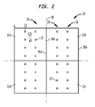
- FIG. 2 is a partial top plan view illustrating a microelectronic substrate 20 , e.g., a portion 20 of a wafer 10 , containing four microelectronic elements 12 a , 12 b , 12 c , and 12 d , e.g., semiconductor chips, each having edges defined by dicing lanes 14 .
- the wafer 10 remains intact such that the portion remains connected with the remainder of the wafer.
- the processes described in the following can be performed in relation to microelectronic substrates smaller than a complete wafer, such as a substrate which includes one microelectronic element (one chip), a few chips or many chips.
- Contacts, e.g., bond pads, lands, etc., of the chips 12 are shown at 22 .
- the contacts typically are laid out in parallel rows, a first row of contacts 24 of chip 12 b being adjacent to a first edge 34 b and a second row 26 of contacts being adjacent to a second edge 36 b of chip 12 b .
- a second row 26 of contacts of chip 12 a is adjacent to a second edge 36 a of that chip.
- One or more alignment markings 42 on the substrate may be used to determine and maintain the orientation of the substrate in the plane defined by the major surface of the substrate.
- FIG. 3 illustrates a subsequent stage of processing in which traces 40 are fabricated on each chip of the substrate 20 a .
- Layout directions in form of familiar compass directions are indicated by legend 92 .
- the reference to compass directions is for convenience in identifying relative directions between elements in the following description.
- the elements described in the following may or may not be aligned with the true directions of a compass.
- the traces are connected to and extend from the contacts 22 towards edges of each chip.
- the traces may extend from the contacts towards left and right edges (north-south direction) edges 34 , 36 of each chip and not towards the top and bottom edges (east-west direction) edges 44 , 46 of each chip.
- the traces can be manufactured in a semiconductor fabrication facility as conductors extending along a surface of an external passivation layer of the chip at or above the level of the contacts 22 .
- the traces can be provided during fabrication of a “redistribution layer”, which can be constructed either during fabrication in the semiconductor fabrication facility or in subsequent processes, such as those performed in a facility which packages the wafer or a portion of a wafer into packaged chips.
- traces 40 L can extend in parallel paths from contacts 22 on chip 12 a towards edges 34 a , 36 a .
- Traces 40 R can also extend from contacts 22 on chip 12 b towards edges 34 b , 36 b , which may be in parallel paths.
- the traces can extend all the way to the dicing lanes 14 along adjacent edges between chips 12 a , 12 b and between chips 12 c and 12 d .
- the substrate shown in FIG. 3 is oriented the same way as the substrate illustrated in FIG. 2 .
- a monument of the substrate e.g., an alignment marking 42 , flat side 16 ( FIG. 1 ), etc. has the same position on the substrate shown in FIG. 3 as it does in FIG. 2 .
- the orientation of the substrate 20 a in FIG. 3 can also be identified by the location of the marker “A” at the upper left hand corner of the figure.
- the traces 40 L extend towards left edges 34 of the chips and are connected to top edges of the contacts.
- traces 40 R extend towards right edges 36 of the chip and are connected to bottom edges of the contacts. In such way, the traces 40 R on the right side of each chip in FIG. 3 are displaced downwardly by the same amount that the traces 40 L on the left side of each chip are displaced upwardly.
- the substrate in the orientation shown in FIG. 3 will be referred to as substrate 20 a.
- FIG. 4 illustrates a substrate 20 b having identical construction as illustrated in FIG. 3 , but in which an orientation of the chips 12 a , 12 b , 12 c , 12 d therein is reversed in relation to that shown in FIG. 3 .
- the reverse orientation can be understood from the location of the marker “A” in the upper right hand corner of the figure and the location of the alignment marking 42 on chip 12 a .
- the edges 34 a , 34 b are aligned with the right hand side of each chip.
- Traces 40 L which extend towards the right-hand edges 34 a , 34 b of the chips are displaced upwardly, while the traces 40 R which extend towards left-hand edges 36 a , 36 b are displaced downwardly.
- Such orientation is achieved when the substrate 20 a shown in FIG. 3 is flipped such that its active surface (see 50 b , FIG. 6 ) faces down rather than up (the direction in which active surface 50 a ( FIG. 6 ) faces.
- FIG. 5 is a sectional view through line 5 - 5 of FIG. 3 .
- substrate 20 a has contacts 22 exposed at the major (active) surface 50 a .
- a terminal “exposed at” a surface of a dielectric element may be flush with such surface, recessed relative to such surface, or protruding from such surface, so long as the terminal is accessible for contact by a theoretical point moving towards the surface in a direction perpendicular to the surface.
- trace 40 L is visible because of the relative downward or upward layout displacement of left-hand traces 40 L relative to right-hand traces 40 R ( FIG. 3 ) of each chip, as discussed above.
- FIG. 5 represents a stage in fabrication of a stacked assembly including a plurality of chips stacked and interconnected together in one package.
- a stacked assembly 70 a includes a substrate 20 b mounted to substrate 20 a with an adhesive layer 52 a .
- the substrates are mounted such that active face 50 b of substrate 20 b confronts active face 50 a of substrate 20 a .
- the upper substrate 20 b has the reverse orientation ( FIG. 4 ) relative to the lower substrate 20 a , such that edge 34 a of a chip of substrate 20 b is aligned with edge 36 b of a chip of substrate 20 a .
- trace 40 Lb of the upper substrate 20 b is not aligned with trace 40 La on substrate 20 a .
- FIG. 7 is a corresponding plan view illustrating the location of traces of both substrates after the two substrates have been joined together. Traces including trace 40 La of the lower substrate are indicated by areas without hatching. The traces of the upper substrate, including trace 40 Lb are shown with hatching. FIG. 7 shows the location of the traces 40 La, 40 Ra of the lower substrate in relation to traces 40 Lb, 40 Rb of the upper substrate. At edge regions 56 of the chips, none of the traces of each substrate is aligned with any other traces. As will be described in more detail below, this feature allows stacked assemblies of chips to be fabricated in which a plurality of essentially co-planar leads can be formed which connect to each chip individually.
- the non-overlapping character of the traces present at each edge of a chip permit the traces of a chip at each level in the stack to be connected to individual leads which are insulated from the leads of chips at other (higher or lower) levels in the stack. Connections to the chips in the stack need not be made only through leads which are common to a plurality of chips.
- FIG. 8 illustrates a substrate 20 c having identical construction as the substrate 20 a illustrated in FIG. 3 , but in which an orientation of the chips 12 a , 12 b , 12 c , 12 d therein is horizontally and vertically reversed in relation to that shown in FIG. 3 .
- the orientation can be understood from the location of the marker “A” in the lower left hand corner of the figure and the location of the alignment marking 42 on chip 12 a .
- the edges 34 a , 34 b are disposed towards the left hand side of each chip but are now towards the lower part of the figure.
- Traces 40 L which extend towards the left-hand edges 34 a , 34 b of the chips are displaced downwardly towards the edges 44 of the chips, while the traces 40 R which extend towards right-hand edges 36 a , 36 b are displaced upwardly towards edges 46 .
- the orientation of substrate 20 c in FIG. 8 can be achieved by flipping the substrate 20 a ( FIG. 3 ) vertically and rotating it within the plane of its active surface.
- the stacked assembly shown in FIG. 9 is inverted such that substrate 20 c lies at the bottom of the assembly, as shown.
- the thickness of substrate 20 a then is reduced and edge regions are removed and filled with a dielectric.
- an additional substrate 20 d having the orientation shown in FIG. 11 is mounted to the stacked assembly using an adhesive layer 52 c ( FIG. 10 ).
- substrate 20 d also is thinned and edge portions are removed and filled with a dielectric, as described above ( FIG. 6 ) to form a stacked assembly 230 .
- the substrate 20 d is oriented in a fourth way, as indicated by marker “A” and alignment marking 42 .
- the orientation of substrate 20 d is different from each of the orientations of substrates 20 a , 20 b and 20 c .
- traces 40 L of substrate 20 c are both displaced downwardly and towards the right-hand edges 34 a of chip 12 a .
- the substrate 20 a FIG. 3
- the substrate 20 a can be rotated in the plane of its active surface.
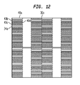
- FIG. 12 is a plan view illustrating the relative positions of the traces of each substrate 20 a , 20 b , 20 c and 20 d in the stacked assembly. While the traces are disposed on the substrates at different levels of the stacked assembly, the relative positions of the traces are shown in a manner as if the stacked assembly were transparent. For ease of reference, traces of substrate 20 a are referenced as 40 a , traces of substrate 20 b referenced 40 b , the traces of substrate 20 c are referenced 40 c and the traces of substrate 20 d referenced 40 d . As seen in FIG. 12 , at least at first and second edges of each individual chip, e.g., edges 34 a , 36 a , none of the traces of the vertically stacked chips are registered with each other.
- FIG. 13 illustrates a subsequent stage of fabrication in which a series of notches 246 are formed in the stacked assembly 230 .
- Notches can be formed by mechanical, chemical or optical, e.g., laser ablation means, as described, for example, in commonly owned U.S. Pat. Nos. 5,455,455; 6,646,289; and 7,192,796, which are incorporated by reference herein.
- the notches are aligned with the dicing lanes 14 of the substrates. As seen in the sectional view provided in FIG.
- microelectronic elements e.g., 212 of a first substrate 210 are aligned with the microelectronic elements 212 A of a second substrate 210 A, the microelectronic elements 212 B of the third substrate 210 B, and the microelectronic elements 212 C of the third substrate 210 C.
- Notches 246 are aligned with traces 224 , 224 ′, 224 A, 224 A′, 224 B, 224 B′, 224 C, 224 C′ on the microelectronic elements.
- the stacked assembly 230 consists of a plurality of stacked and adhered microelectronic elements 212 , 212 A, 212 B, 212 C oriented and aligned in various rows and columns.
- the notches 246 are cut from the stacked assembly 230 at locations that are proximate respective first edges 218 , 218 A, 218 B, and 218 C, second edges 220 , 220 A, 220 B and 220 C of the respective microelectronic elements 212 , 212 A, 212 B and 212 C of the various substrates 210 , 210 A, 210 B, and 210 C.
- the notches 246 are formed at the saw lanes 14 by the methods described for the earlier embodiments. As seen in FIG. 13 , the plurality of notches 246 are cut through the adhesive layers 243 , 243 A, 243 B, 243 C.
- the notches 246 do not extend entirely through the stacked assembly 230 but rather extend only partially into relief cavities 208 , 208 ′ which contain dielectric material between adjacent microelectronic elements.
- a carrier layer or additional substrate 202 remains intact to connect the stacked microelectronic elements and is protected from cracking because adhesive in the relief cavities 208 , 208 ′ rather that the substrate is cut.
- the notches 246 are illustrated having inclined side walls 248 , 250 , the side walls may also be straight.
- the stacked assembly 230 of FIG. 13 includes four individual wafers/substrates stacked one upon another. In alternative embodiments the stacked assembly 230 may include less or more wafers/substrates positioned on top of each other.
- leads 266 FIG. 14 may be formed on the inclined side walls 248 , 250 of notches 246 .
- the inclined side walls 248 , 250 extend through at least part of the various first, second, third and fourth substrates 210 , 210 A, 210 B and 210 C exposed at walls of the notches 246 .
- Leads 266 may then be formed by any suitable metal deposition technique.
- the leads 266 may be formed by depositing a primary metal layer, e.g., by sputtering, electroless deposition, etc., along edges of the substrates 210 exposed within the notches.
- the primary metal layer can then be photolithographically patterned into separate leads, followed by electroplating to increase the thickness of leads and if desired, form leads having multiple different metal layers.
- the leads 266 extend within the various notches 246 , and establish electrical contact with the traces 224 , 224 A, 224 B and 224 C on the respective substrates 210 , 210 A, 210 B and 210 C.
- the leads 266 extend along the side walls 248 , 250 of notches 246 and adhere to the adhesive layer 243 C on the upper surface 216 C of the fourth substrate 210 C.
- the leads 266 can include ends 275 remote from notches 246 and exposed at the surface of adhesive layer 243 C. Pads or solder bumps may be provided at the ends 275 of the leads 266 .
- Each lead 266 preferably is in contact with only one of the four traces 224 , 224 A, 224 B, 224 C as a result of the traces being non-aligned with each other within the plane of the sectional view shown in FIG. 14 , as apparent from the plan view ( FIG. 12 ) discussed above.
- traces 224 , 224 A, 224 B, 224 C are positioned in different planes that reside closer or farther away from the section of the stacked assembly which is visible in FIG. 14 .
- an insulative solder mask or other dielectric layer 277 may be patterned over the surface of adhesive layer 216 C and over the leads 266 , leaving pads or solder bumps at the ends 275 of the traces exposed.
- leads 266 may be extended to the bottom surface of the substrate 202 .
- the leads 266 extend along the side walls 248 , 250 of notches 246 and enter the adhesive layer 209 within the relief cavity 208 positioned below the first substrate 210 .
- the bottom of leads 266 may be exposed below the lower surface of the stacked assembly 230 and the leads may be extended by the methods previously discussed to create bottom leads 286 .
- Solder mask 227 may be patterned over the bottom surface of substrate 202 for the attachment of wires or solder bumps to allow the formation of pads or bumps at the ends 288 .
- a particular advantage of this arrangement is that either stacked assemblies 230 or individual packages may in turn be stacked and electrically interconnected, one upon the other by aligning and connecting the respective top ends 275 and bottom ends 288 of the leads, such as through use of solder bumps.
- the top ends 275 and bottom ends 288 can be aligned in an appropriate pattern extending in one or more directions defined by the planes of the top faces 282 and the bottom faces 284 of the stacked assembly.
- the stacked assembly may be severed, e.g., by sawing, scribing and breaking or otherwise dicing along the dicing lanes 218 , 220 into individual packaged units 280 .
- the stacked assembly may be severed into individual packages by mechanically sawing through the leads 266 , the adhesive 209 and the substrate 202 . The saw cuts are aligned with notches 246 such that the notches 246 are extended entirely through the thickness of the stacked assembly 230 .
- Each of the resulting stacked packaged assemblies 280 includes a plurality of microelectronic elements, e.g., semiconductor device chips, stacked one upon another.
- the resulting stacked individual unit 280 shown in FIG. 18 may be externally connected to an interconnection element such as a substrate, circuit board or circuit panel via wire bonding or via pads 275 or solder bumps 274 ( FIG. 19 ).
- each stacked assembly 280 having small thickness. Where substrates of 25-30 microns each are stacked in forming the assemblies, packages incorporating four or more stacked chips, with thicknesses of approximately 155 microns or less can be achieved.
- each individual lead 266 of a stacked assembly can be connected to as few as one trace of just one microelectronic element. In this way, selection of individual microelectronic elements is made possible with granularity at the level of the individual microelectronic element.
- three stacked assemblies 280 of the type shown in FIG. 18 or FIG. 19 may be stacked and interconnected.
- Bond wires 2202 , 2202 ′, 2202 ′′ connecting lands 2204 , 2204 ′ and 2204 ′′ of the stacked assemblies provide interconnection to terminals 2206 of a circuit panel 2210 .
- the bond wires may be arranged to connect lands of adjacent levels as shown in FIG. 20 or each bond wire may directly connect a stacked assembly to the circuit panel. Alternatively, some of the bond wires connected to a particular stacked assembly may be connected to another stacked assembly which is not adjacent to the particular stacked assembly.
- a face 2220 ′′ of a stacked assembly 280 ′′ and a land 2204 ′′ thereon extends beyond a face 2220 ′ and an edge 2222 ′ of stacked assembly 280 ′ and a land 2204 ′ thereon, thus permitting the lands 2204 ′ and 2204 ′′ to be interconnected using bond wire 2202 ′.
- a face 2220 ′ of the stacked assembly 280 ′ and the land 2204 ′ thereon extends beyond a face 2220 and an edge 2222 of stacked assembly 230 and a land 2204 thereon, thus permitting the lands 2204 ′ and 2204 to be interconnected using bond wire 2202 .
- FIG. 21 is a front plan view illustrating a microelectronic substrate 320 a having a plurality of microelectronic elements 312 a , 312 b , 312 c , 312 d , etc., in which contacts 322 on a front face 324 of the microelectronic element are disposed adjacent to left and right (north-south) edges 334 a , 336 a defined by dicing lanes 314 .
- Traces 340 A connected to contacts 322 adjacent to edge 336 a extend towards a top edge 338 a of the microelectronic element.
- traces 340 B connected to contacts 322 extend towards a bottom edge 342 a of the microelectronic element.
- the traces 340 A and 340 B may reach the top and bottom edges 338 a and 342 a.
- FIG. 22 is a rear plan view illustrating a microelectronic substrate 320 b having the same characteristics as the substrate 320 a of FIG. 21 , where the substrate has been flipped over such that the view in FIG. 22 looks towards a rear face 326 of the microelectronic substrate. Because the substrate has been flipped over, the traces now appear to extend in opposite directions from those of FIG. 21 .
- FIG. 23 illustrates still another case in which the microelectronic substrate 320 c has the same characteristics as the substrate 320 a ( FIG. 21 ) but which is rotated 180 degrees from the orientation shown in FIG. 21 .
- edge 336 c of substrate 320 c is aligned with edge 334 a of substrate 320 a .
- edge 334 c of substrate of substrate 320 c is aligned with edge 336 a of substrate 320 a .
- traces 340 A adjacent to edge 336 c are not be in the same locations as traces 340 B ( FIG.
- each of traces 340 A of substrate 320 c adjacent to that edge are spaced from traces 340 B ( FIG. 21 ) such that each individual trace 340 A, 340 B is spaced apart from every other trace where it meets the top or bottom edge 338 a , 342 a.
- FIG. 24 illustrates still another case in which the microelectronic substrate 320 d has the same characteristics as the substrate 320 a ( FIG. 21 ) but which is rotated 180 degrees and flipped over from the orientation shown in FIG. 21 .
- substrate 320 d is stacked with substrate 320 b in one stacked assembly, traces of the microelectronic substrate shown in FIG. 24 are spaced apart from traces of the microelectronic substrate 320 b ( FIG. 22 ).
- FIG. 25 is a plan view illustrating a stacked packaged assembly 380 which includes microelectronic elements of each of the substrates 320 a , 320 b , 320 c , and 320 d ( FIGS. 21-25 ) stacked and joined in the orientations illustrated in FIGS. 21-25 .
- the traces 340 at edges of the packaged assembly are spaced apart such that external connection can be made to each individual trace 340 of the assembly, as described above.
- Steps to fabricate leads and to sever a stacked assembly into an individual stacked packaged assembly such as the one shown at 380 are similar to that described above.
- FIG. 26 is a plan view illustrating a stacked packaged assembly 480 according to a variation of the above embodiment in which traces, e.g., traces 440 A of each microelectronic element extend only from contacts, e.g., contacts 422 a , along a limited extent of a first edge 434 a .
- Traces 440 B of a second substrate extend only from contacts 422 b along another limited portion of the first edge 434 a .
- Traces 440 C of a third substrate extend only from contacts 422 c along another limited portion of the first edge 436 a .
- Traces 440 D of a fourth substrate extend only from contacts 422 d along another limited portion of the first edge 436 a .
- traces at edges 438 a and 442 a of the stacked packaged assembly 480 are spaced apart, facilitating interconnection of leads of the stacked assembly to individual traces of individual microelectronic elements of the assembly.
Landscapes
- Engineering & Computer Science (AREA)
- Microelectronics & Electronic Packaging (AREA)
- Power Engineering (AREA)
- Computer Hardware Design (AREA)
- Physics & Mathematics (AREA)
- Condensed Matter Physics & Semiconductors (AREA)
- General Physics & Mathematics (AREA)
- Manufacturing & Machinery (AREA)
- Wire Bonding (AREA)
Abstract
Description
Claims (7)
Priority Applications (1)
| Application Number | Priority Date | Filing Date | Title |
|---|---|---|---|
| US13/274,815 US8513794B2 (en) | 2007-08-09 | 2011-10-17 | Stacked assembly including plurality of stacked microelectronic elements |
Applications Claiming Priority (3)
| Application Number | Priority Date | Filing Date | Title |
|---|---|---|---|
| US96406907P | 2007-08-09 | 2007-08-09 | |
| US12/221,924 US8043895B2 (en) | 2007-08-09 | 2008-08-07 | Method of fabricating stacked assembly including plurality of stacked microelectronic elements |
| US13/274,815 US8513794B2 (en) | 2007-08-09 | 2011-10-17 | Stacked assembly including plurality of stacked microelectronic elements |
Related Parent Applications (1)
| Application Number | Title | Priority Date | Filing Date |
|---|---|---|---|
| US12/221,924 Division US8043895B2 (en) | 2007-08-09 | 2008-08-07 | Method of fabricating stacked assembly including plurality of stacked microelectronic elements |
Publications (2)
| Publication Number | Publication Date |
|---|---|
| US20120032349A1 US20120032349A1 (en) | 2012-02-09 |
| US8513794B2 true US8513794B2 (en) | 2013-08-20 |
Family
ID=40345713
Family Applications (2)
| Application Number | Title | Priority Date | Filing Date |
|---|---|---|---|
| US12/221,924 Active 2028-09-23 US8043895B2 (en) | 2007-08-09 | 2008-08-07 | Method of fabricating stacked assembly including plurality of stacked microelectronic elements |
| US13/274,815 Active US8513794B2 (en) | 2007-08-09 | 2011-10-17 | Stacked assembly including plurality of stacked microelectronic elements |
Family Applications Before (1)
| Application Number | Title | Priority Date | Filing Date |
|---|---|---|---|
| US12/221,924 Active 2028-09-23 US8043895B2 (en) | 2007-08-09 | 2008-08-07 | Method of fabricating stacked assembly including plurality of stacked microelectronic elements |
Country Status (1)
| Country | Link |
|---|---|
| US (2) | US8043895B2 (en) |
Families Citing this family (33)
| Publication number | Priority date | Publication date | Assignee | Title |
|---|---|---|---|---|
| US7901989B2 (en) | 2006-10-10 | 2011-03-08 | Tessera, Inc. | Reconstituted wafer level stacking |
| US8513789B2 (en) | 2006-10-10 | 2013-08-20 | Tessera, Inc. | Edge connect wafer level stacking with leads extending along edges |
| US7829438B2 (en) | 2006-10-10 | 2010-11-09 | Tessera, Inc. | Edge connect wafer level stacking |
| US7952195B2 (en) | 2006-12-28 | 2011-05-31 | Tessera, Inc. | Stacked packages with bridging traces |
| KR101458538B1 (en) | 2007-07-27 | 2014-11-07 | 테세라, 인코포레이티드 | A stacked microelectronic unit, and method of fabrication thereof |
| KR101533663B1 (en) | 2007-08-03 | 2015-07-03 | 테세라, 인코포레이티드 | Stack packages using reconstituted wafers |
| US8043895B2 (en) | 2007-08-09 | 2011-10-25 | Tessera, Inc. | Method of fabricating stacked assembly including plurality of stacked microelectronic elements |
| CN105140134A (en) | 2007-09-28 | 2015-12-09 | 泰塞拉公司 | Flip chip interconnection with double post |
| WO2009154761A1 (en) | 2008-06-16 | 2009-12-23 | Tessera Research Llc | Stacking of wafer-level chip scale packages having edge contacts |
| KR100997787B1 (en) * | 2008-06-30 | 2010-12-02 | 주식회사 하이닉스반도체 | Stacked semiconductor package and method of manufacturing the same |
| US8466542B2 (en) | 2009-03-13 | 2013-06-18 | Tessera, Inc. | Stacked microelectronic assemblies having vias extending through bond pads |
| US8435082B2 (en) * | 2010-08-03 | 2013-05-07 | Tyco Electronics Corporation | Electrical connectors and printed circuits having broadside-coupling regions |
| US20110221053A1 (en) * | 2010-03-11 | 2011-09-15 | Qualcomm Incorporated | Pre-processing to reduce wafer level warpage |
| US8580607B2 (en) | 2010-07-27 | 2013-11-12 | Tessera, Inc. | Microelectronic packages with nanoparticle joining |
| US8853558B2 (en) | 2010-12-10 | 2014-10-07 | Tessera, Inc. | Interconnect structure |
| JP6022792B2 (en) * | 2012-03-30 | 2016-11-09 | 国立大学法人東北大学 | Integrated device and manufacturing method of integrated device |
| US9093457B2 (en) * | 2012-08-22 | 2015-07-28 | Freescale Semiconductor Inc. | Stacked microelectronic packages having patterned sidewall conductors and methods for the fabrication thereof |
| US9064977B2 (en) | 2012-08-22 | 2015-06-23 | Freescale Semiconductor Inc. | Stacked microelectronic packages having sidewall conductors and methods for the fabrication thereof |
| US9190390B2 (en) * | 2012-08-22 | 2015-11-17 | Freescale Semiconductor Inc. | Stacked microelectronic packages having sidewall conductors and methods for the fabrication thereof |
| US9299670B2 (en) | 2013-03-14 | 2016-03-29 | Freescale Semiconductor, Inc. | Stacked microelectronic packages having sidewall conductors and methods for the fabrication thereof |
| US9789380B2 (en) | 2013-03-25 | 2017-10-17 | Flex Booth, Inc. | System and method for tracking fitness progress from a server |
| US9524950B2 (en) | 2013-05-31 | 2016-12-20 | Freescale Semiconductor, Inc. | Stacked microelectronic packages having sidewall conductors and methods for the fabrication thereof |
| US9025340B2 (en) | 2013-09-30 | 2015-05-05 | Freescale Semiconductor, Inc. | Devices and stacked microelectronic packages with in-trench package surface conductors and methods of their fabrication |
| US9036363B2 (en) | 2013-09-30 | 2015-05-19 | Freescale Semiconductor, Inc. | Devices and stacked microelectronic packages with parallel conductors and intra-conductor isolator structures and methods of their fabrication |
| US9305911B2 (en) | 2013-12-05 | 2016-04-05 | Freescale Semiconductor, Inc. | Devices and stacked microelectronic packages with package surface conductors and adjacent trenches and methods of their fabrication |
| US9263420B2 (en) | 2013-12-05 | 2016-02-16 | Freescale Semiconductor, Inc. | Devices and stacked microelectronic packages with package surface conductors and methods of their fabrication |
| US9595485B2 (en) * | 2014-06-26 | 2017-03-14 | Nxp Usa, Inc. | Microelectronic packages having embedded sidewall substrates and methods for the producing thereof |
| US10388607B2 (en) | 2014-12-17 | 2019-08-20 | Nxp Usa, Inc. | Microelectronic devices with multi-layer package surface conductors and methods of their fabrication |
| US9633971B2 (en) | 2015-07-10 | 2017-04-25 | Invensas Corporation | Structures and methods for low temperature bonding using nanoparticles |
| US10886250B2 (en) | 2015-07-10 | 2021-01-05 | Invensas Corporation | Structures and methods for low temperature bonding using nanoparticles |
| CA2908289A1 (en) * | 2015-10-14 | 2017-04-14 | Fourth Dimension Designs Ltd. | Plunger impact sensor |
| US9728509B1 (en) * | 2016-05-05 | 2017-08-08 | Globalfoundries Inc. | Laser scribe structures for a wafer |
| TWI822659B (en) | 2016-10-27 | 2023-11-21 | 美商艾德亞半導體科技有限責任公司 | Structures and methods for low temperature bonding |
Citations (243)
| Publication number | Priority date | Publication date | Assignee | Title |
|---|---|---|---|---|
| US4074342A (en) | 1974-12-20 | 1978-02-14 | International Business Machines Corporation | Electrical package for lsi devices and assembly process therefor |
| US4500905A (en) | 1981-09-30 | 1985-02-19 | Tokyo Shibaura Denki Kabushiki Kaisha | Stacked semiconductor device with sloping sides |
| US4765864A (en) | 1987-07-15 | 1988-08-23 | Sri International | Etching method for producing an electrochemical cell in a crystalline substrate |
| US4842699A (en) | 1988-05-10 | 1989-06-27 | Avantek, Inc. | Method of selective via-hole and heat sink plating using a metal mask |
| US4897708A (en) | 1986-07-17 | 1990-01-30 | Laser Dynamics, Inc. | Semiconductor wafer array |
| US4954875A (en) | 1986-07-17 | 1990-09-04 | Laser Dynamics, Inc. | Semiconductor wafer array with electrically conductive compliant material |
| US5322816A (en) | 1993-01-19 | 1994-06-21 | Hughes Aircraft Company | Method for forming deep conductive feedthroughs |
| US5343071A (en) | 1993-04-28 | 1994-08-30 | Raytheon Company | Semiconductor structures having dual surface via holes |
| FR2704690A1 (en) | 1993-04-27 | 1994-11-04 | Thomson Csf | Method for encapsulating semiconductor wafers, device obtained by this process and application to the interconnection of wafers in three dimensions. |
| US5412539A (en) | 1993-10-18 | 1995-05-02 | Hughes Aircraft Company | Multichip module with a mandrel-produced interconnecting decal |
| US5424245A (en) | 1994-01-04 | 1995-06-13 | Motorola, Inc. | Method of forming vias through two-sided substrate |
| US5426072A (en) | 1993-01-21 | 1995-06-20 | Hughes Aircraft Company | Process of manufacturing a three dimensional integrated circuit from stacked SOI wafers using a temporary silicon substrate |
| US5466634A (en) | 1994-12-20 | 1995-11-14 | International Business Machines Corporation | Electronic modules with interconnected surface metallization layers and fabrication methods therefore |
| DE19516487C1 (en) | 1995-05-05 | 1996-07-25 | Fraunhofer Ges Forschung | Vertical integration process for microelectronic system |
| US5563084A (en) | 1994-09-22 | 1996-10-08 | Fraunhofer-Gesellschaft zur F orderung der angewandten Forschung e.V. | Method of making a three-dimensional integrated circuit |
| US5571754A (en) | 1995-07-26 | 1996-11-05 | International Business Machines Corporation | Method of fabrication of endcap chip with conductive, monolithic L-connect for multichip stack |
| US5604673A (en) | 1995-06-07 | 1997-02-18 | Hughes Electronics | Low temperature co-fired ceramic substrates for power converters |
| US5608264A (en) | 1995-06-05 | 1997-03-04 | Harris Corporation | Surface mountable integrated circuit with conductive vias |
| US5614766A (en) | 1991-09-30 | 1997-03-25 | Rohm Co., Ltd. | Semiconductor device with stacked alternate-facing chips |
| US5618752A (en) | 1995-06-05 | 1997-04-08 | Harris Corporation | Method of fabrication of surface mountable integrated circuits |
| US5646067A (en) | 1995-06-05 | 1997-07-08 | Harris Corporation | Method of bonding wafers having vias including conductive material |
| US5656553A (en) | 1994-08-22 | 1997-08-12 | International Business Machines Corporation | Method for forming a monolithic electronic module by dicing wafer stacks |
| US5661087A (en) | 1994-06-23 | 1997-08-26 | Cubic Memory, Inc. | Vertical interconnect process for silicon segments |
| US5682062A (en) | 1995-06-05 | 1997-10-28 | Harris Corporation | System for interconnecting stacked integrated circuits |
| US5716759A (en) | 1993-09-02 | 1998-02-10 | Shellcase Ltd. | Method and apparatus for producing integrated circuit devices |
| US5767001A (en) | 1993-05-05 | 1998-06-16 | Siemens Aktiengesellschaft | Process for producing semiconductor components between which contact is made vertically |
| US5766984A (en) | 1994-09-22 | 1998-06-16 | Fraunhofer-Gesellschaft Zur Foerderung Der Angewandten Forschung | Method of making a vertical integrated circuit |
| US5804004A (en) | 1992-05-11 | 1998-09-08 | Nchip, Inc. | Stacked devices for multichip modules |
| US5814889A (en) | 1995-06-05 | 1998-09-29 | Harris Corporation | Intergrated circuit with coaxial isolation and method |
| US5817530A (en) | 1996-05-20 | 1998-10-06 | Micron Technology, Inc. | Use of conductive lines on the back side of wafers and dice for semiconductor interconnects |
| WO1998045130A1 (en) | 1997-04-04 | 1998-10-15 | Leedy Glenn J | Three dimensional structure memory |
| US5880010A (en) | 1994-07-12 | 1999-03-09 | Sun Microsystems, Inc. | Ultrathin electronics |
| EP0926723A1 (en) | 1997-11-26 | 1999-06-30 | STMicroelectronics S.r.l. | Process for forming front-back through contacts in micro-integrated electronic devices |
| WO1999040624A1 (en) | 1998-02-06 | 1999-08-12 | Shellcase Ltd. | Integrated circuit device |
| US5946545A (en) | 1994-03-30 | 1999-08-31 | Internatinal Business Machines Corporation | Semiconductor stack structures and fabrication/sparing methods utilizing programmable spare circuit |
| US5973386A (en) | 1996-02-16 | 1999-10-26 | Nec Corporation | Semiconductor substrate having silicon oxide layers formed between polysilicon layers |
| US6002167A (en) | 1995-09-22 | 1999-12-14 | Hitachi Cable, Ltd. | Semiconductor device having lead on chip structure |
| US6022758A (en) | 1994-07-10 | 2000-02-08 | Shellcase Ltd. | Process for manufacturing solder leads on a semiconductor device package |
| US6031274A (en) | 1996-10-11 | 2000-02-29 | Hamamatsu Photonics K.K. | Back irradiation type light-receiving device and method of making the same |
| US6040235A (en) | 1994-01-17 | 2000-03-21 | Shellcase Ltd. | Methods and apparatus for producing integrated circuit devices |
| US6103552A (en) | 1998-08-10 | 2000-08-15 | Lin; Mou-Shiung | Wafer scale packaging scheme |
| EP1041624A1 (en) | 1999-04-02 | 2000-10-04 | Interuniversitair Microelektronica Centrum Vzw | Method of transferring ultra-thin substrates and application of the method to the manufacture of a multilayer thin film device |
| US6130823A (en) | 1999-02-01 | 2000-10-10 | Raytheon E-Systems, Inc. | Stackable ball grid array module and method |
| US6177707B1 (en) | 1998-03-02 | 2001-01-23 | U.S. Philips Corporation | Semiconductor device comprising a glass supporting body onto which a substrate with semiconductor elements and a metalization is attached by means of an adhesive |
| US6177721B1 (en) | 1998-10-21 | 2001-01-23 | Hyundai Electronics Industries Co., Ltd | Chip stack-type semiconductor package and method for fabricating the same |
| JP2001035995A (en) | 1999-07-22 | 2001-02-09 | Seiko Epson Corp | Method of forming through hole of semiconductor chip |
| US6188129B1 (en) | 1997-03-24 | 2001-02-13 | Hyundai Electronics Industries Co., Ltd. | Stacked semiconductor chip package having external terminal pads and stackable chips having a protection layer |
| US6204562B1 (en) | 1999-02-11 | 2001-03-20 | United Microelectronics Corp. | Wafer-level chip scale package |
| US6228686B1 (en) | 1995-09-18 | 2001-05-08 | Tessera, Inc. | Method of fabricating a microelectronic assembly using sheets with gaps to define lead regions |
| US6252305B1 (en) * | 2000-02-29 | 2001-06-26 | Advanced Semiconductor Engineering, Inc. | Multichip module having a stacked chip arrangement |
| US6261865B1 (en) | 1998-10-06 | 2001-07-17 | Micron Technology, Inc. | Multi chip semiconductor package and method of construction |
| JP2001210782A (en) | 2000-01-27 | 2001-08-03 | Seiko Epson Corp | Semiconductor chip, multi-chip package, semiconductor device, and electronic equipment using it |
| JP2001217386A (en) | 2000-02-03 | 2001-08-10 | Seiko Epson Corp | Semiconductor device, method of manufacturing the same, and electronic equipment |
| US6277669B1 (en) | 1999-09-15 | 2001-08-21 | Industrial Technology Research Institute | Wafer level packaging method and packages formed |
| US20010024839A1 (en) | 1998-12-17 | 2001-09-27 | Lin Charles Wen Chyang | Bumpless flip chip assembly with strips-in-via and plating |
| US20010048151A1 (en) | 1998-05-30 | 2001-12-06 | Hyundai Electronics Industries Co., Inc. | Stackable ball grid array semiconductor package and fabrication method thereof |
| US6340845B1 (en) | 1999-01-22 | 2002-01-22 | Nec Corporation | Memory package implementing two-fold memory capacity and two different memory functions |
| US6344401B1 (en) | 2000-03-09 | 2002-02-05 | Atmel Corporation | Method of forming a stacked-die integrated circuit chip package on a water level |
| JP2002093944A (en) | 2000-09-11 | 2002-03-29 | Oki Electric Ind Co Ltd | Semiconductor device and its manufacturing method, and stack-type semiconductor device and its manufacturing method |
| US6396710B1 (en) | 2000-05-12 | 2002-05-28 | Raytheon Company | High density interconnect module |
| US20020074637A1 (en) | 2000-12-19 | 2002-06-20 | Intel Corporation | Stacked flip chip assemblies |
| US20020109236A1 (en) | 2001-02-09 | 2002-08-15 | Samsung Electronics Co., Ltd. | Three-dimensional multi-chip package having chip selection pads and manufacturing method thereof |
| US20020113303A1 (en) | 2000-12-18 | 2002-08-22 | Kei Murayama | Mounting structure for semiconductor devices |
| US20020127775A1 (en) | 1999-12-23 | 2002-09-12 | Rambus Inc. | Redistributed bond pads in stacked integrated circuit die package |
| US20020132465A1 (en) | 1997-04-04 | 2002-09-19 | Elm Technology Corporation | Reconfigurable integrated circuit memory |
| US6472293B2 (en) | 1999-04-13 | 2002-10-29 | Oki Electric Industry Co., Ltd. | Method for manufacturing an interconnect structure for stacked semiconductor device |
| US6472247B1 (en) | 2000-06-26 | 2002-10-29 | Ricoh Company, Ltd. | Solid-state imaging device and method of production of the same |
| US20020171145A1 (en) | 2001-05-21 | 2002-11-21 | Akifumi Higuchi | BGA type semiconductor device, tape carrier for semiconductor device, and semiconductor device using said tape carrier |
| US6486546B2 (en) * | 1998-08-21 | 2002-11-26 | Micron Technology, Inc. | Low profile multi-IC chip package connector |
| US6492201B1 (en) | 1998-07-10 | 2002-12-10 | Tessera, Inc. | Forming microelectronic connection components by electrophoretic deposition |
| US6498387B1 (en) | 2000-02-15 | 2002-12-24 | Wen-Ken Yang | Wafer level package and the process of the same |
| US6498381B2 (en) | 2001-02-22 | 2002-12-24 | Tru-Si Technologies, Inc. | Semiconductor structures having multiple conductive layers in an opening, and methods for fabricating same |
| US20030006494A1 (en) | 2001-07-03 | 2003-01-09 | Lee Sang Ho | Thin profile stackable semiconductor package and method for manufacturing |
| JP2003037758A (en) | 2001-01-12 | 2003-02-07 | Konica Corp | Imaging unit |
| US6548391B1 (en) | 1999-05-27 | 2003-04-15 | Fraunhofer-Gesellschaft Zur Foerderung Der Angewandten Forschung E. V. | Method of vertically integrating electric components by means of back contacting |
| US6562653B1 (en) | 1999-01-11 | 2003-05-13 | Intel Corporation | Silicon interposer and multi-chip-module (MCM) with through substrate vias |
| US20030096454A1 (en) | 2001-11-16 | 2003-05-22 | Poo Chia Yong | Stackable semiconductor package and wafer level fabrication method |
| JP2003163324A (en) | 2001-11-27 | 2003-06-06 | Nec Corp | Unit semiconductor device and manufacturing method thereof, and three-dimensional laminated semiconductor device |
| US6582991B1 (en) | 2000-12-14 | 2003-06-24 | Matsushita Electric Industrial Co., Ltd. | Semiconductor device and method for fabricating the same |
| JP2003208655A (en) | 2002-01-16 | 2003-07-25 | Hitachi Ltd | Automatic transaction device |
| US6607941B2 (en) | 2002-01-11 | 2003-08-19 | National Semiconductor Corporation | Process and structure improvements to shellcase style packaging technology |
| US6608377B2 (en) | 2001-01-30 | 2003-08-19 | Samsung Electronics Co., Ltd. | Wafer level package including ground metal layer |
| US6607938B2 (en) | 2001-07-19 | 2003-08-19 | Samsung Electronics Co., Ltd. | Wafer level stack chip package and method for manufacturing same |
| US6621155B1 (en) | 1999-12-23 | 2003-09-16 | Rambus Inc. | Integrated circuit device having stacked dies and impedance balanced transmission lines |
| US6624505B2 (en) | 1998-02-06 | 2003-09-23 | Shellcase, Ltd. | Packaged integrated circuits and methods of producing thereof |
| US20030209772A1 (en) | 2002-05-13 | 2003-11-13 | National Semiconductor Corporation | Electrical die contact structure and fabrication method |
| US6656827B1 (en) | 2002-10-17 | 2003-12-02 | Taiwan Semiconductor Manufacturing Co., Ltd. | Electrical performance enhanced wafer level chip scale package with ground |
| US20030233704A1 (en) | 2000-04-17 | 2003-12-25 | Miguel Castellote | Air massage system for bathtub |
| US20040014255A1 (en) | 2002-07-22 | 2004-01-22 | Grigg Ford B. | Thick solder mask for confining encapsulant material over selected locations of a substrate, assemblies including the solder mask, and methods |
| US20040016942A1 (en) | 2002-04-24 | 2004-01-29 | Seiko Epson Corporation | Semiconductor device and a method of manufacturing the same, a circuit board and an electronic apparatus |
| US6693358B2 (en) | 2000-10-23 | 2004-02-17 | Matsushita Electric Industrial Co., Ltd. | Semiconductor chip, wiring board and manufacturing process thereof as well as semiconductor device |
| JP2004063569A (en) | 2002-07-25 | 2004-02-26 | Seiko Epson Corp | Semiconductor device and manufacturing method therefor, circuit board, and electronic apparatus |
| WO2004025727A1 (en) | 2002-09-10 | 2004-03-25 | Frank Niklaus | Method for sealing a microcavity and package comprising at least one microcavity |
| US6717254B2 (en) | 2001-02-22 | 2004-04-06 | Tru-Si Technologies, Inc. | Devices having substrates with opening passing through the substrates and conductors in the openings, and methods of manufacture |
| JP2004119473A (en) | 2002-09-24 | 2004-04-15 | Seiko Epson Corp | Semiconductor device, its manufacturing method, circuit board, and electronic apparatus |
| US6727576B2 (en) | 2001-10-31 | 2004-04-27 | Infineon Technologies Ag | Transfer wafer level packaging |
| US20040082114A1 (en) | 2002-10-29 | 2004-04-29 | Chih-Horng Horng | Fabrication method of window-type ball grid array semiconductor package |
| US6737300B2 (en) | 2001-01-24 | 2004-05-18 | Advanced Semiconductor Engineering, Inc. | Chip scale package and manufacturing method |
| JP2004153130A (en) | 2002-10-31 | 2004-05-27 | Olympus Corp | Semiconductor device and its manufacturing method |
| US6743660B2 (en) | 2002-01-12 | 2004-06-01 | Taiwan Semiconductor Manufacturing Co., Ltd | Method of making a wafer level chip scale package |
| US20040104454A1 (en) | 2002-10-10 | 2004-06-03 | Rohm Co., Ltd. | Semiconductor device and method of producing the same |
| JP2004158536A (en) | 2002-11-05 | 2004-06-03 | Fujitsu Ltd | Semiconductor device and method for manufacturing the same |
| US6753208B1 (en) | 1998-03-20 | 2004-06-22 | Mcsp, Llc | Wafer scale method of packaging integrated circuit die |
| US6753205B2 (en) | 2001-09-13 | 2004-06-22 | Tru-Si Technologies, Inc. | Method for manufacturing a structure comprising a substrate with a cavity and a semiconductor integrated circuit bonded to a contact pad located in the cavity |
| US20040155354A1 (en) | 2000-06-02 | 2004-08-12 | Seiko Epson Corporation | Semiconductor device, method of fabricating the same, stack-type semiconductor device, circuit board and electronic instrument |
| US6777767B2 (en) | 1999-12-10 | 2004-08-17 | Shellcase Ltd. | Methods for producing packaged integrated circuit devices & packaged integrated circuit devices produced thereby |
| US6784023B2 (en) | 1996-05-20 | 2004-08-31 | Micron Technology, Inc. | Method of fabrication of stacked semiconductor devices |
| US20040169278A1 (en) | 2001-05-21 | 2004-09-02 | Kinsman Larry D. | Bumped die and wire bonded board-on-chip package |
| US6806559B2 (en) | 2002-04-22 | 2004-10-19 | Irvine Sensors Corporation | Method and apparatus for connecting vertically stacked integrated circuit chips |
| US20040221451A1 (en) | 2003-05-06 | 2004-11-11 | Micron Technology, Inc. | Method for packaging circuits and packaged circuits |
| US20040222508A1 (en) | 2003-03-18 | 2004-11-11 | Akiyoshi Aoyagi | Semiconductor device, electronic device, electronic apparatus, method of manufacturing semiconductor device, and method of manufacturing electronic device |
| EP1482553A2 (en) | 2003-05-26 | 2004-12-01 | Sanyo Electric Co., Ltd. | Semiconductor device and manufacturing method thereof |
| US6828175B2 (en) | 2002-08-29 | 2004-12-07 | Micron Technology, Inc. | Semiconductor component with backside contacts and method of fabrication |
| US20040251525A1 (en) | 2003-06-16 | 2004-12-16 | Shellcase Ltd. | Methods and apparatus for packaging integrated circuit devices |
| WO2004114397A1 (en) | 2003-06-20 | 2004-12-29 | Koninklijke Philips Electronics N.V. | Electronic device, assembly and methods of manufacturing an electronic device |
| US20050003649A1 (en) | 2003-06-09 | 2005-01-06 | Sanyo Electric Co., Ltd. | Semiconductor device and manufacturing method thereof |
| US6844619B2 (en) | 2000-12-01 | 2005-01-18 | Nec Corporation | Compact semiconductor device capable of mounting a plurality of semiconductor chips with high density and method of manufacturing the same |
| US20050012225A1 (en) | 2002-11-15 | 2005-01-20 | Choi Seung-Yong | Wafer-level chip scale package and method for fabricating and using the same |
| US20050046002A1 (en) | 2003-08-26 | 2005-03-03 | Kang-Wook Lee | Chip stack package and manufacturing method thereof |
| US6864172B2 (en) | 2002-06-18 | 2005-03-08 | Sanyo Electric Co., Ltd. | Manufacturing method of semiconductor device |
| US20050051883A1 (en) | 2003-06-19 | 2005-03-10 | Seiko Epson Corporation | Semiconductor device and method of manufacturing the same, circuit board, and electronic instrument |
| US6867123B2 (en) | 2001-02-08 | 2005-03-15 | Renesas Technology Corp. | Semiconductor integrated circuit device and its manufacturing method |
| US20050056903A1 (en) | 2003-08-28 | 2005-03-17 | Satoshi Yamamoto | Semiconductor package and method of manufacturing same |
| US6870249B2 (en) | 2002-12-24 | 2005-03-22 | Oki Electric Industry Co., Ltd. | Semiconductor device and manufacturing method thereof |
| EP1519410A1 (en) | 2003-09-25 | 2005-03-30 | Interuniversitair Microelektronica Centrum vzw ( IMEC) | Method for producing electrical through hole interconnects and devices made thereof |
| US20050067680A1 (en) | 2003-09-30 | 2005-03-31 | Boon Suan Jeung | Castellated chip-scale packages and methods for fabricating the same |
| US20050073035A1 (en) | 2003-09-19 | 2005-04-07 | Moxham Stephen F. | Semiconductor component having stiffener and circuit decal and method of fabrication |
| US6878608B2 (en) | 2001-05-31 | 2005-04-12 | International Business Machines Corporation | Method of manufacture of silicon based package |
| JP2005101067A (en) | 2003-09-22 | 2005-04-14 | Sharp Corp | Wiring structure of substrate and wiring forming method |
| US20050095835A1 (en) | 2003-09-26 | 2005-05-05 | Tessera, Inc. | Structure and method of making capped chips having vertical interconnects |
| US20050104179A1 (en) | 2003-07-03 | 2005-05-19 | Shellcase Ltd. | Methods and apparatus for packaging integrated circuit devices |
| US6897148B2 (en) | 2003-04-09 | 2005-05-24 | Tru-Si Technologies, Inc. | Electroplating and electroless plating of conductive materials into openings, and structures obtained thereby |
| US20050156330A1 (en) | 2004-01-21 | 2005-07-21 | Harris James M. | Through-wafer contact to bonding pad |
| DE102004039906A1 (en) | 2004-08-18 | 2005-08-18 | Infineon Technologies Ag | Electronic component with a number of integrated members, is formed by producing members with a surface that contains a circuit, and connecting components using bond wires |
| WO2005081315A2 (en) | 2004-02-18 | 2005-09-01 | Infineon Technologies Ag | Semiconductor component comprising a stack of semiconductor chips and method for producing the same |
| JP2005303031A (en) | 2004-04-13 | 2005-10-27 | Matsushita Electric Ind Co Ltd | Electronic circuit module, multilayer electronic circuit module and their manufacturing methods |
| US20050260794A1 (en) | 2002-09-03 | 2005-11-24 | Industrial Technology Research Institute | Method for fabrication of wafer level package incorporating dual compliant layers |
| US20050263866A1 (en) | 2004-05-27 | 2005-12-01 | Chang-Fegn Wan | Hermetic pacakging and method of manufacture and use therefore |
| US6972483B1 (en) | 2004-06-30 | 2005-12-06 | Hynix Semiconductor Inc. | Semiconductor package with improved thermal emission property |
| US20050287783A1 (en) | 2004-06-29 | 2005-12-29 | Kirby Kyle K | Microelectronic devices and methods for forming interconnects in microelectronic devices |
| US6984885B1 (en) | 2000-02-10 | 2006-01-10 | Renesas Technology Corp. | Semiconductor device having densely stacked semiconductor chips |
| US20060006488A1 (en) | 2004-06-30 | 2006-01-12 | Sony Corporation | Solid-state imaging device, camera and method of producing the solid-state imaging device |
| EP1619722A1 (en) | 2003-04-16 | 2006-01-25 | Hamamatsu Photonics K. K. | Method for manufacturing backside-illuminated optical sensor |
| US20060017161A1 (en) | 2004-07-22 | 2006-01-26 | Jae-Sik Chung | Semiconductor package having protective layer for re-routing lines and method of manufacturing the same |
| US20060046348A1 (en) | 2004-09-01 | 2006-03-02 | Kang Byoung Y | Semiconductor chip packages and methods for fabricating the same |
| US20060043556A1 (en) | 2004-08-25 | 2006-03-02 | Chao-Yuan Su | Stacked packaging methods and structures |
| US20060046471A1 (en) | 2004-08-27 | 2006-03-02 | Kirby Kyle K | Methods for forming vias of varying lateral dimensions and semiconductor components and assemblies including same |
| US20060043601A1 (en) | 2002-11-14 | 2006-03-02 | Wolfgang Pahl | Hermetically encapsulated component and waferscale method for the production thereof |
| US20060043598A1 (en) | 2004-08-31 | 2006-03-02 | Kirby Kyle K | Methods of manufacture of a via structure comprising a plurality of conductive elements, semiconductor die, multichip module, and system including same |
| US20060055061A1 (en) | 2004-09-02 | 2006-03-16 | Ryuji Hosokawa | Semiconductor device and a method of assembling a semiconductor device |
| WO2006027981A1 (en) | 2004-09-08 | 2006-03-16 | Matsushita Electric Industrial Co., Ltd. | Stereoscopic electronic circuit device, electronic device using the same, and method for manufacturing the same |
| US20060055050A1 (en) | 2004-09-10 | 2006-03-16 | Hideo Numata | Semiconductor device and manufacturing method thereof |
| US20060068580A1 (en) | 2004-09-28 | 2006-03-30 | Sharp Kabushiki Kaisha | Semiconductor device and fabrication method thereof |
| US20060076670A1 (en) | 2004-10-08 | 2006-04-13 | Lim Ohk K | Micro-electro-mechanical system (MEMS) package having metal sealing member |
| US20060079019A1 (en) | 2004-10-08 | 2006-04-13 | Easetech Korea Co., Ltd. | Method for manufacturing wafer level chip scale package using redistribution substrate |
| US7034401B2 (en) | 2003-12-17 | 2006-04-25 | Tru-Si Technologies, Inc. | Packaging substrates for integrated circuits and soldering methods |
| EP1653510A2 (en) | 2004-10-28 | 2006-05-03 | Sanyo Electric Co., Ltd. | Semiconductor device and manufacturing method of the same |
| US20060094165A1 (en) | 2004-10-29 | 2006-05-04 | Harry Hedler | Method for fabricating semiconductor components |
| US7049170B2 (en) | 2003-12-17 | 2006-05-23 | Tru-Si Technologies, Inc. | Integrated circuits and packaging substrates with cavities, and attachment methods including insertion of protruding contact pads into cavities |
| US20060115932A1 (en) | 1997-12-18 | 2006-06-01 | Farnworth Warren M | Method for fabricating semiconductor components with conductive vias |
| US20060138626A1 (en) | 2004-12-29 | 2006-06-29 | Tessera, Inc. | Microelectronic packages using a ceramic substrate having a window and a conductive surface region |
| EP1686627A1 (en) | 2005-01-28 | 2006-08-02 | Samsung Electro-Mechanics Co., Ltd. | Semiconductor package and method of manufacturing the same |
| US7087459B2 (en) | 2002-12-30 | 2006-08-08 | Dongbu Electronics Co., Ltd. | Method for packaging a multi-chip module of a semiconductor device |
| US20060175697A1 (en) | 2005-02-02 | 2006-08-10 | Tetsuya Kurosawa | Semiconductor device having semiconductor chips stacked and mounted thereon and manufacturing method thereof |
| US7115986B2 (en) | 2001-05-02 | 2006-10-03 | Micron Technology, Inc. | Flexible ball grid array chip scale packages |
| US20060220234A1 (en) | 2005-03-22 | 2006-10-05 | Tessera, Inc. | Wire bonded wafer level cavity package |
| US20060220262A1 (en) | 2005-04-04 | 2006-10-05 | Torsten Meyer | Stacked die package |
| US20060249829A1 (en) | 2005-04-08 | 2006-11-09 | Mitsuaki Katagiri | Stacked type semiconductor device |
| US20060258044A1 (en) | 2005-05-11 | 2006-11-16 | Infineon Technologies Ag | Method of manufacturing a semiconductor device comprising stacked chips and a corresponding semiconductor device |
| US20060292866A1 (en) | 2005-06-23 | 2006-12-28 | Borwick Robert L | Low temperature method for fabricating high-aspect ratio vias and devices fabricated by said method |
| US7160753B2 (en) | 2004-03-16 | 2007-01-09 | Voxtel, Inc. | Silicon-on-insulator active pixel sensors |
| EP1741668A2 (en) | 2005-07-05 | 2007-01-10 | Shinko Electric Industries Co., Ltd. | Method for encasing a MEMS device and packaged device |
| US20070007556A1 (en) | 2003-07-23 | 2007-01-11 | Hamamatsu Photonics K.K. | Backside-illuminated photodetector |
| US20070035001A1 (en) | 2005-08-11 | 2007-02-15 | Jochen Kuhmann | Chip scale package for a micro component |
| US20070037379A1 (en) | 2005-08-11 | 2007-02-15 | Ziptronix | 3D IC method and device |
| US20070045803A1 (en) | 2005-08-26 | 2007-03-01 | Micron Technology, Inc. | Microelectronic device packages, stacked microelectronic device packages, and methods for manufacturing microelectronic devices |
| US20070045862A1 (en) | 2005-09-01 | 2007-03-01 | Micron Technology, Inc. | Stacked microelectronic devices and methods for manufacturing microelectronic devices |
| US20070052050A1 (en) | 2005-09-07 | 2007-03-08 | Bart Dierickx | Backside thinned image sensor with integrated lens stack |
| US7208343B2 (en) * | 2002-02-06 | 2007-04-24 | Samsung Electronics Co., Ltd. | Semiconductor chip, chip stack package and manufacturing method |
| US7215018B2 (en) | 2004-04-13 | 2007-05-08 | Vertical Circuits, Inc. | Stacked die BGA or LGA component assembly |
| US20070102802A1 (en) | 2003-09-19 | 2007-05-10 | Samsung Electronics Co., Ltd. | Single chip and stack-type chip semiconductor package and method of manufacturing the same |
| US20070126085A1 (en) | 2005-12-02 | 2007-06-07 | Nec Electronics Corporation | Semiconductor device and method of manufacturing the same |
| WO2007066409A1 (en) | 2005-12-09 | 2007-06-14 | Spansion Llc | Semiconductor device and its manufacturing method |
| US20070132082A1 (en) | 2005-12-12 | 2007-06-14 | Intel Corporation | Copper plating connection for multi-die stack in substrate package |
| EP1801866A2 (en) | 2002-11-05 | 2007-06-27 | Shinko Electric Industries Co., Ltd. | Semiconductor device and method of manufacturing the same |
| US20070148941A1 (en) | 2005-12-27 | 2007-06-28 | Tessera, Inc. | Microelectronic component with photo-imageable substrate |
| US20070158807A1 (en) | 2005-12-29 | 2007-07-12 | Daoqiang Lu | Edge interconnects for die stacking |
| US20070181989A1 (en) | 2006-02-08 | 2007-08-09 | Micron Technology, Inc. | Microelectronic devices, stacked microelectronic devices, and methods for manufacturing such devices |
| US20070190747A1 (en) | 2006-01-23 | 2007-08-16 | Tessera Technologies Hungary Kft. | Wafer level packaging to lidded chips |
| US7285865B2 (en) | 2005-07-15 | 2007-10-23 | Samsung Electronic Co., Ltd. | Micro-package, multi-stack micro-package, and manufacturing method therefor |
| US20070257350A1 (en) | 2003-11-19 | 2007-11-08 | Kang-Wook Lee | Wafer level stack structure for system-in-package and method thereof |
| US7312521B2 (en) | 2002-04-23 | 2007-12-25 | Sanyo Electric Co., Ltd. | Semiconductor device with holding member |
| US20080083976A1 (en) | 2006-10-10 | 2008-04-10 | Tessera, Inc. | Edge connect wafer level stacking |
| US20080083977A1 (en) | 2006-10-10 | 2008-04-10 | Tessera, Inc. | Edge connect wafer level stacking |
| US20080090333A1 (en) | 2006-10-17 | 2008-04-17 | Tessera, Inc. | Microelectronic packages fabricated at the wafer level and methods therefor |
| US20080099900A1 (en) | 2006-10-31 | 2008-05-01 | Tessera Technologies Hungary Kft. | Wafer-level fabrication of lidded chips with electrodeposited dielectric coating |
| US20080099907A1 (en) | 2006-10-31 | 2008-05-01 | Tessera Technologies Hungary Kft. | Wafer-level fabrication of lidded chips with electrodeposited dielectric coating |
| US20080116545A1 (en) | 2006-11-22 | 2008-05-22 | Tessera, Inc. | Packaged semiconductor chips |
| US20080116544A1 (en) | 2006-11-22 | 2008-05-22 | Tessera, Inc. | Packaged semiconductor chips with array |
| US20080122113A1 (en) * | 2006-08-17 | 2008-05-29 | Corisis David J | Semiconductor device assemblies and systems including at least one conductive pathway extending around a side of at least one semiconductor device and methods for forming the same |
| US7394152B2 (en) | 2006-11-13 | 2008-07-01 | China Wafer Level Csp Ltd. | Wafer level chip size packaged chip device with an N-shape junction inside and method of fabricating the same |
| US20080157327A1 (en) | 2007-01-03 | 2008-07-03 | Advanced Chip Engineering Technology Inc. | Package on package structure for semiconductor devices and method of the same |
| US20080166836A1 (en) | 2003-06-03 | 2008-07-10 | Casio Computer Co., Ltd. | Semiconductor package including connected upper and lower interconnections, and manufacturing method thereof |
| US7408249B2 (en) | 1998-02-06 | 2008-08-05 | Tessera Technologies Hungary Kft. | Packaged integrated circuits and methods of producing thereof |
| US20080246136A1 (en) | 2007-03-05 | 2008-10-09 | Tessera, Inc. | Chips having rear contacts connected by through vias to front contacts |
| US20080284041A1 (en) | 2007-05-18 | 2008-11-20 | Samsung Electronics Co., Ltd. | Semiconductor package with through silicon via and related method of fabrication |
| US20080308921A1 (en) | 2007-06-18 | 2008-12-18 | Jong Hoon Kim | Molded reconfigured wafer, stack package using the same, and method for manufacturing the stack package |
| US20080315407A1 (en) | 2007-06-20 | 2008-12-25 | Vertical Circuits, Inc. | Three-dimensional circuitry formed on integrated circuit device using two-dimensional fabrication |
| US20090009491A1 (en) | 2007-07-04 | 2009-01-08 | Grivna Edward L | Capacitive sensing control knob |
| US20090032966A1 (en) | 2007-08-01 | 2009-02-05 | Jong Ho Lee | Method of fabricating a 3-D device and device made thereby |
| WO2009017835A2 (en) | 2007-07-31 | 2009-02-05 | Tessera, Inc. | Semiconductor packaging process using through silicon vias |
| WO2009017758A2 (en) | 2007-07-27 | 2009-02-05 | Tessera, Inc. | Reconstituted wafer stack packaging with after-applied pad extensions |
| US20090039528A1 (en) | 2007-08-09 | 2009-02-12 | Tessera, Inc. | Wafer level stacked packages with individual chip selection |
| WO2009023462A1 (en) | 2007-08-10 | 2009-02-19 | Spansion Llc | Semiconductor device and method for manufacturing thereof |
| US7498661B2 (en) | 2003-03-25 | 2009-03-03 | Seiko Epson Corporation | Manufacturing method for semiconductor device, semiconductor device, and electronic apparatus |
| US20090067135A1 (en) | 2005-05-02 | 2009-03-12 | Advanced Systems Japan Inc. | Semiconductor Package Having Socket Function, Semiconductor Module, Electronic Circuit Module and Circuit Board with Socket |
| US7510928B2 (en) | 2006-05-05 | 2009-03-31 | Tru-Si Technologies, Inc. | Dielectric trenches, nickel/tantalum oxide structures, and chemical mechanical polishing techniques |
| US20090121323A1 (en) | 2007-11-08 | 2009-05-14 | Samsung Electronics Co., Ltd | Semiconductor device and method of fabricating the same |
| US20090160065A1 (en) | 2006-10-10 | 2009-06-25 | Tessera, Inc. | Reconstituted Wafer Level Stacking |
| US20090166846A1 (en) | 2007-12-28 | 2009-07-02 | Micron Technology, Inc. | Pass-through 3d interconnect for microelectronic dies and associated systems and methods |
| US20090166840A1 (en) | 2007-12-27 | 2009-07-02 | Samsung Electronics Co., Ltd. | Wafer-level stack package |
| US20090212381A1 (en) | 2008-02-26 | 2009-08-27 | Tessera, Inc. | Wafer level packages for rear-face illuminated solid state image sensors |
| US7622810B2 (en) | 2002-10-11 | 2009-11-24 | Sanyo Electric Co., Ltd. | Semiconductor device and manufacturing method thereof |
| US20090309235A1 (en) | 2008-06-11 | 2009-12-17 | Stats Chippac, Ltd. | Method and Apparatus for Wafer Level Integration Using Tapered Vias |
| US20090316378A1 (en) | 2008-06-16 | 2009-12-24 | Tessera Research Llc | Wafer level edge stacking |
| US7662670B2 (en) | 2002-10-30 | 2010-02-16 | Sanyo Electric Co., Ltd. | Manufacturing method of semiconductor device |
| US7663213B2 (en) | 2006-11-13 | 2010-02-16 | China Wafer Level Csp Ltd. | Wafer level chip size packaged chip device with a double-layer lead structure and method of fabricating the same |
| US7662710B2 (en) | 2006-09-26 | 2010-02-16 | Hymite A/S | Formation of through-wafer electrical interconnections and other structures using a thin dielectric membrane |
| US20100053407A1 (en) | 2008-02-26 | 2010-03-04 | Tessera, Inc. | Wafer level compliant packages for rear-face illuminated solid state image sensors |
| US20100065949A1 (en) | 2008-09-17 | 2010-03-18 | Andreas Thies | Stacked Semiconductor Chips with Through Substrate Vias |
| US20100164086A1 (en) | 2006-08-11 | 2010-07-01 | Sanyo Electric Co., Ltd. | Semiconductor device and manufacturing method thereof |
| US20100200966A1 (en) | 2002-09-17 | 2010-08-12 | Marcos Karnezos | Semiconductor multi-package module having package stacked over die-up flip chip ball grid array package and having wire bond interconnect between stacked packages |
| US20100219523A1 (en) | 2006-02-27 | 2010-09-02 | Seng Guan Chow | Stackable integrated circuit package system |
| US20100230795A1 (en) | 2009-03-13 | 2010-09-16 | Tessera Technologies Hungary Kft. | Stacked microelectronic assemblies having vias extending through bond pads |
| US7859115B2 (en) | 2008-11-07 | 2010-12-28 | Hynix Semiconductor Inc. | Semiconductor package for improving characteristics for transmitting signals and power |
| US20110024890A1 (en) | 2007-06-29 | 2011-02-03 | Stats Chippac, Ltd. | Stackable Package By Using Internal Stacking Modules |
| US7884459B2 (en) * | 2003-01-15 | 2011-02-08 | Fujitsu Semiconductor Limited | Semiconductor device suitable for a stacked structure |
| US20110039370A1 (en) | 2005-07-21 | 2011-02-17 | Shinko Electric Industries Co., Ltd. | Electronic parts packaging structure and method of manufacturing the same |
| US7944015B2 (en) | 2007-07-27 | 2011-05-17 | Sanyo Electric Co., Ltd. | Semiconductor device and method of manufacturing the same |
| US7952195B2 (en) | 2006-12-28 | 2011-05-31 | Tessera, Inc. | Stacked packages with bridging traces |
| US7973416B2 (en) | 2008-05-12 | 2011-07-05 | Texas Instruments Incorporated | Thru silicon enabled die stacking scheme |
| US20110198722A1 (en) | 2007-08-16 | 2011-08-18 | Hynix Semiconductor Inc. | Semiconductor package through-electrode suitable for a stacked semiconductor package and semiconductor package having the same |
| US20110248410A1 (en) | 2007-08-03 | 2011-10-13 | Tessera, Inc. | Stack packages using reconstituted wafers |
Family Cites Families (1)
| Publication number | Priority date | Publication date | Assignee | Title |
|---|---|---|---|---|
| JPS60160645A (en) | 1984-02-01 | 1985-08-22 | Hitachi Ltd | Laminated semiconductor integrated circuit device |
-
2008
- 2008-08-07 US US12/221,924 patent/US8043895B2/en active Active
-
2011
- 2011-10-17 US US13/274,815 patent/US8513794B2/en active Active
Patent Citations (306)
| Publication number | Priority date | Publication date | Assignee | Title |
|---|---|---|---|---|
| US4074342A (en) | 1974-12-20 | 1978-02-14 | International Business Machines Corporation | Electrical package for lsi devices and assembly process therefor |
| US4500905A (en) | 1981-09-30 | 1985-02-19 | Tokyo Shibaura Denki Kabushiki Kaisha | Stacked semiconductor device with sloping sides |
| US4897708A (en) | 1986-07-17 | 1990-01-30 | Laser Dynamics, Inc. | Semiconductor wafer array |
| US4954875A (en) | 1986-07-17 | 1990-09-04 | Laser Dynamics, Inc. | Semiconductor wafer array with electrically conductive compliant material |
| US4765864A (en) | 1987-07-15 | 1988-08-23 | Sri International | Etching method for producing an electrochemical cell in a crystalline substrate |
| US4842699A (en) | 1988-05-10 | 1989-06-27 | Avantek, Inc. | Method of selective via-hole and heat sink plating using a metal mask |
| US5614766A (en) | 1991-09-30 | 1997-03-25 | Rohm Co., Ltd. | Semiconductor device with stacked alternate-facing chips |
| US5804004A (en) | 1992-05-11 | 1998-09-08 | Nchip, Inc. | Stacked devices for multichip modules |
| US5322816A (en) | 1993-01-19 | 1994-06-21 | Hughes Aircraft Company | Method for forming deep conductive feedthroughs |
| US5426072A (en) | 1993-01-21 | 1995-06-20 | Hughes Aircraft Company | Process of manufacturing a three dimensional integrated circuit from stacked SOI wafers using a temporary silicon substrate |
| WO1994025987A1 (en) | 1993-04-27 | 1994-11-10 | Thomson-Csf | Semiconductor chip encapsulation method, device produced by this method and its application to three dimensional chip interconnection |
| FR2704690A1 (en) | 1993-04-27 | 1994-11-04 | Thomson Csf | Method for encapsulating semiconductor wafers, device obtained by this process and application to the interconnection of wafers in three dimensions. |
| US5343071A (en) | 1993-04-28 | 1994-08-30 | Raytheon Company | Semiconductor structures having dual surface via holes |
| US5767001A (en) | 1993-05-05 | 1998-06-16 | Siemens Aktiengesellschaft | Process for producing semiconductor components between which contact is made vertically |
| US5716759A (en) | 1993-09-02 | 1998-02-10 | Shellcase Ltd. | Method and apparatus for producing integrated circuit devices |
| US5412539A (en) | 1993-10-18 | 1995-05-02 | Hughes Aircraft Company | Multichip module with a mandrel-produced interconnecting decal |
| US5424245A (en) | 1994-01-04 | 1995-06-13 | Motorola, Inc. | Method of forming vias through two-sided substrate |
| US6040235A (en) | 1994-01-17 | 2000-03-21 | Shellcase Ltd. | Methods and apparatus for producing integrated circuit devices |
| US5946545A (en) | 1994-03-30 | 1999-08-31 | Internatinal Business Machines Corporation | Semiconductor stack structures and fabrication/sparing methods utilizing programmable spare circuit |
| US5661087A (en) | 1994-06-23 | 1997-08-26 | Cubic Memory, Inc. | Vertical interconnect process for silicon segments |
| US6022758A (en) | 1994-07-10 | 2000-02-08 | Shellcase Ltd. | Process for manufacturing solder leads on a semiconductor device package |
| US5880010A (en) | 1994-07-12 | 1999-03-09 | Sun Microsystems, Inc. | Ultrathin electronics |
| US5656553A (en) | 1994-08-22 | 1997-08-12 | International Business Machines Corporation | Method for forming a monolithic electronic module by dicing wafer stacks |
| US5563084A (en) | 1994-09-22 | 1996-10-08 | Fraunhofer-Gesellschaft zur F orderung der angewandten Forschung e.V. | Method of making a three-dimensional integrated circuit |
| US5766984A (en) | 1994-09-22 | 1998-06-16 | Fraunhofer-Gesellschaft Zur Foerderung Der Angewandten Forschung | Method of making a vertical integrated circuit |
| US5466634A (en) | 1994-12-20 | 1995-11-14 | International Business Machines Corporation | Electronic modules with interconnected surface metallization layers and fabrication methods therefore |
| DE19516487C1 (en) | 1995-05-05 | 1996-07-25 | Fraunhofer Ges Forschung | Vertical integration process for microelectronic system |
| US5618752A (en) | 1995-06-05 | 1997-04-08 | Harris Corporation | Method of fabrication of surface mountable integrated circuits |
| US5608264A (en) | 1995-06-05 | 1997-03-04 | Harris Corporation | Surface mountable integrated circuit with conductive vias |
| US5814889A (en) | 1995-06-05 | 1998-09-29 | Harris Corporation | Intergrated circuit with coaxial isolation and method |
| US5646067A (en) | 1995-06-05 | 1997-07-08 | Harris Corporation | Method of bonding wafers having vias including conductive material |
| US5682062A (en) | 1995-06-05 | 1997-10-28 | Harris Corporation | System for interconnecting stacked integrated circuits |
| US5604673A (en) | 1995-06-07 | 1997-02-18 | Hughes Electronics | Low temperature co-fired ceramic substrates for power converters |
| US5571754A (en) | 1995-07-26 | 1996-11-05 | International Business Machines Corporation | Method of fabrication of endcap chip with conductive, monolithic L-connect for multichip stack |
| US6228686B1 (en) | 1995-09-18 | 2001-05-08 | Tessera, Inc. | Method of fabricating a microelectronic assembly using sheets with gaps to define lead regions |
| US6002167A (en) | 1995-09-22 | 1999-12-14 | Hitachi Cable, Ltd. | Semiconductor device having lead on chip structure |
| US5973386A (en) | 1996-02-16 | 1999-10-26 | Nec Corporation | Semiconductor substrate having silicon oxide layers formed between polysilicon layers |
| US6784023B2 (en) | 1996-05-20 | 2004-08-31 | Micron Technology, Inc. | Method of fabrication of stacked semiconductor devices |
| US20060121645A1 (en) | 1996-05-20 | 2006-06-08 | Ball Michael B | Method of fabrication of stacked semiconductor devices |
| US5817530A (en) | 1996-05-20 | 1998-10-06 | Micron Technology, Inc. | Use of conductive lines on the back side of wafers and dice for semiconductor interconnects |
| US6031274A (en) | 1996-10-11 | 2000-02-29 | Hamamatsu Photonics K.K. | Back irradiation type light-receiving device and method of making the same |
| US6188129B1 (en) | 1997-03-24 | 2001-02-13 | Hyundai Electronics Industries Co., Ltd. | Stacked semiconductor chip package having external terminal pads and stackable chips having a protection layer |
| WO1998045130A1 (en) | 1997-04-04 | 1998-10-15 | Leedy Glenn J | Three dimensional structure memory |
| US7193239B2 (en) | 1997-04-04 | 2007-03-20 | Elm Technology Corporation | Three dimensional structure integrated circuit |
| US7138295B2 (en) | 1997-04-04 | 2006-11-21 | Elm Technology Corporation | Method of information processing using three dimensional integrated circuits |
| US6133640A (en) | 1997-04-04 | 2000-10-17 | Elm Technology Corporation | Three-dimensional structure memory |
| US7474004B2 (en) | 1997-04-04 | 2009-01-06 | Elm Technology Corporation | Three dimensional structure memory |
| US20090067210A1 (en) | 1997-04-04 | 2009-03-12 | Leedy Glenn J | Three dimensional structure memory |
| US7504732B2 (en) | 1997-04-04 | 2009-03-17 | Elm Technology Corporation | Three dimensional structure memory |
| US20090174082A1 (en) | 1997-04-04 | 2009-07-09 | Glenn J Leedy | Three dimensional structure memory |
| US5915167A (en) | 1997-04-04 | 1999-06-22 | Elm Technology Corporation | Three dimensional structure memory |
| US20090175104A1 (en) | 1997-04-04 | 2009-07-09 | Leedy Glenn J | Three dimensional structure memory |
| US6208545B1 (en) | 1997-04-04 | 2001-03-27 | Glenn J. Leedy | Three dimensional structure memory |
| US20020132465A1 (en) | 1997-04-04 | 2002-09-19 | Elm Technology Corporation | Reconfigurable integrated circuit memory |
| US20090219744A1 (en) | 1997-04-04 | 2009-09-03 | Leedy Glenn J | Three dimensional structure memory |
| US20040070063A1 (en) | 1997-04-04 | 2004-04-15 | Elm Technology Corporation | Three dimensional structure integrated circuit |
| US20090218700A1 (en) | 1997-04-04 | 2009-09-03 | Leedy Glenn J | Three dimensional structure memory |
| US20090219742A1 (en) | 1997-04-04 | 2009-09-03 | Leedy Glenn J | Three dimensional structure memory |
| US20090219772A1 (en) | 1997-04-04 | 2009-09-03 | Leedy Glenn J | Three dimensional structure memory |
| US20090219743A1 (en) | 1997-04-04 | 2009-09-03 | Leedy Glenn J | Three dimensional structure memory |
| US20090230501A1 (en) | 1997-04-04 | 2009-09-17 | Leedy Glenn J | Three dimensional structure memory |
| US7705466B2 (en) | 1997-04-04 | 2010-04-27 | Elm Technology Corporation | Three dimensional multi layer memory and control logic integrated circuit structure |
| US6632706B1 (en) | 1997-04-04 | 2003-10-14 | Elm Technology Corporation | Three dimensional structure integrated circuit fabrication process |
| US20030173608A1 (en) | 1997-04-04 | 2003-09-18 | Elm Technology Corporation | Three dimensional structure integrated circuit |
| US6563224B2 (en) | 1997-04-04 | 2003-05-13 | Elm Technology Corporation | Three dimensional structure integrated circuit |
| US6551857B2 (en) | 1997-04-04 | 2003-04-22 | Elm Technology Corporation | Three dimensional structure integrated circuits |
| EP0926723A1 (en) | 1997-11-26 | 1999-06-30 | STMicroelectronics S.r.l. | Process for forming front-back through contacts in micro-integrated electronic devices |
| US20060115932A1 (en) | 1997-12-18 | 2006-06-01 | Farnworth Warren M | Method for fabricating semiconductor components with conductive vias |
| US6624505B2 (en) | 1998-02-06 | 2003-09-23 | Shellcase, Ltd. | Packaged integrated circuits and methods of producing thereof |
| WO1999040624A1 (en) | 1998-02-06 | 1999-08-12 | Shellcase Ltd. | Integrated circuit device |
| US6646289B1 (en) | 1998-02-06 | 2003-11-11 | Shellcase Ltd. | Integrated circuit device |
| US7408249B2 (en) | 1998-02-06 | 2008-08-05 | Tessera Technologies Hungary Kft. | Packaged integrated circuits and methods of producing thereof |
| US6177707B1 (en) | 1998-03-02 | 2001-01-23 | U.S. Philips Corporation | Semiconductor device comprising a glass supporting body onto which a substrate with semiconductor elements and a metalization is attached by means of an adhesive |
| US6982475B1 (en) | 1998-03-20 | 2006-01-03 | Mcsp, Llc | Hermetic wafer scale integrated circuit structure |
| US6753208B1 (en) | 1998-03-20 | 2004-06-22 | Mcsp, Llc | Wafer scale method of packaging integrated circuit die |
| US20010048151A1 (en) | 1998-05-30 | 2001-12-06 | Hyundai Electronics Industries Co., Inc. | Stackable ball grid array semiconductor package and fabrication method thereof |
| US6492201B1 (en) | 1998-07-10 | 2002-12-10 | Tessera, Inc. | Forming microelectronic connection components by electrophoretic deposition |
| US6103552A (en) | 1998-08-10 | 2000-08-15 | Lin; Mou-Shiung | Wafer scale packaging scheme |
| US6486546B2 (en) * | 1998-08-21 | 2002-11-26 | Micron Technology, Inc. | Low profile multi-IC chip package connector |
| US6261865B1 (en) | 1998-10-06 | 2001-07-17 | Micron Technology, Inc. | Multi chip semiconductor package and method of construction |
| US6177721B1 (en) | 1998-10-21 | 2001-01-23 | Hyundai Electronics Industries Co., Ltd | Chip stack-type semiconductor package and method for fabricating the same |
| US20010024839A1 (en) | 1998-12-17 | 2001-09-27 | Lin Charles Wen Chyang | Bumpless flip chip assembly with strips-in-via and plating |
| US6562653B1 (en) | 1999-01-11 | 2003-05-13 | Intel Corporation | Silicon interposer and multi-chip-module (MCM) with through substrate vias |
| US6340845B1 (en) | 1999-01-22 | 2002-01-22 | Nec Corporation | Memory package implementing two-fold memory capacity and two different memory functions |
| US6130823A (en) | 1999-02-01 | 2000-10-10 | Raytheon E-Systems, Inc. | Stackable ball grid array module and method |
| US6204562B1 (en) | 1999-02-11 | 2001-03-20 | United Microelectronics Corp. | Wafer-level chip scale package |
| JP2001015683A (en) | 1999-04-02 | 2001-01-19 | Interuniv Micro Electronica Centrum Vzw | Transfer method of ultra-thin substrate and manufacture of multilayer thin film device using the same |
| US6730997B2 (en) | 1999-04-02 | 2004-05-04 | Imec Vzw | Method of transferring ultra-thin substrates and application of the method to the manufacture of a multi-layered thin film device |
| US20030060034A1 (en) | 1999-04-02 | 2003-03-27 | Imec Vzw, A Research Center In The Country Of Belgium | Method of transferring ultra-thin substrates and application of the method to the manufacture of a multi-layer thin film device |
| EP1041624A1 (en) | 1999-04-02 | 2000-10-04 | Interuniversitair Microelektronica Centrum Vzw | Method of transferring ultra-thin substrates and application of the method to the manufacture of a multilayer thin film device |
| US6472293B2 (en) | 1999-04-13 | 2002-10-29 | Oki Electric Industry Co., Ltd. | Method for manufacturing an interconnect structure for stacked semiconductor device |
| US6548391B1 (en) | 1999-05-27 | 2003-04-15 | Fraunhofer-Gesellschaft Zur Foerderung Der Angewandten Forschung E. V. | Method of vertically integrating electric components by means of back contacting |
| JP2001035995A (en) | 1999-07-22 | 2001-02-09 | Seiko Epson Corp | Method of forming through hole of semiconductor chip |
| US6277669B1 (en) | 1999-09-15 | 2001-08-21 | Industrial Technology Research Institute | Wafer level packaging method and packages formed |
| US6777767B2 (en) | 1999-12-10 | 2004-08-17 | Shellcase Ltd. | Methods for producing packaged integrated circuit devices & packaged integrated circuit devices produced thereby |
| US6621155B1 (en) | 1999-12-23 | 2003-09-16 | Rambus Inc. | Integrated circuit device having stacked dies and impedance balanced transmission lines |
| US20020127775A1 (en) | 1999-12-23 | 2002-09-12 | Rambus Inc. | Redistributed bond pads in stacked integrated circuit die package |
| JP2001210782A (en) | 2000-01-27 | 2001-08-03 | Seiko Epson Corp | Semiconductor chip, multi-chip package, semiconductor device, and electronic equipment using it |
| JP2001217386A (en) | 2000-02-03 | 2001-08-10 | Seiko Epson Corp | Semiconductor device, method of manufacturing the same, and electronic equipment |
| US6984885B1 (en) | 2000-02-10 | 2006-01-10 | Renesas Technology Corp. | Semiconductor device having densely stacked semiconductor chips |
| US6498387B1 (en) | 2000-02-15 | 2002-12-24 | Wen-Ken Yang | Wafer level package and the process of the same |
| US6252305B1 (en) * | 2000-02-29 | 2001-06-26 | Advanced Semiconductor Engineering, Inc. | Multichip module having a stacked chip arrangement |
| US6344401B1 (en) | 2000-03-09 | 2002-02-05 | Atmel Corporation | Method of forming a stacked-die integrated circuit chip package on a water level |
| US20030233704A1 (en) | 2000-04-17 | 2003-12-25 | Miguel Castellote | Air massage system for bathtub |
| US6396710B1 (en) | 2000-05-12 | 2002-05-28 | Raytheon Company | High density interconnect module |
| US20040155354A1 (en) | 2000-06-02 | 2004-08-12 | Seiko Epson Corporation | Semiconductor device, method of fabricating the same, stack-type semiconductor device, circuit board and electronic instrument |
| US6472247B1 (en) | 2000-06-26 | 2002-10-29 | Ricoh Company, Ltd. | Solid-state imaging device and method of production of the same |
| JP2002093944A (en) | 2000-09-11 | 2002-03-29 | Oki Electric Ind Co Ltd | Semiconductor device and its manufacturing method, and stack-type semiconductor device and its manufacturing method |
| US20020047199A1 (en) | 2000-09-11 | 2002-04-25 | Shinji Ohuchi | Semiconductor device, manufacturing method of semiconductor device, stack type semiconductor device, and manufacturing method of stack type semiconductor device |
| US6693358B2 (en) | 2000-10-23 | 2004-02-17 | Matsushita Electric Industrial Co., Ltd. | Semiconductor chip, wiring board and manufacturing process thereof as well as semiconductor device |
| US6844619B2 (en) | 2000-12-01 | 2005-01-18 | Nec Corporation | Compact semiconductor device capable of mounting a plurality of semiconductor chips with high density and method of manufacturing the same |
| US6582991B1 (en) | 2000-12-14 | 2003-06-24 | Matsushita Electric Industrial Co., Ltd. | Semiconductor device and method for fabricating the same |
| US20020113303A1 (en) | 2000-12-18 | 2002-08-22 | Kei Murayama | Mounting structure for semiconductor devices |
| US20020074637A1 (en) | 2000-12-19 | 2002-06-20 | Intel Corporation | Stacked flip chip assemblies |
| JP2003037758A (en) | 2001-01-12 | 2003-02-07 | Konica Corp | Imaging unit |
| US6737300B2 (en) | 2001-01-24 | 2004-05-18 | Advanced Semiconductor Engineering, Inc. | Chip scale package and manufacturing method |
| US6608377B2 (en) | 2001-01-30 | 2003-08-19 | Samsung Electronics Co., Ltd. | Wafer level package including ground metal layer |
| US6867123B2 (en) | 2001-02-08 | 2005-03-15 | Renesas Technology Corp. | Semiconductor integrated circuit device and its manufacturing method |
| US20020109236A1 (en) | 2001-02-09 | 2002-08-15 | Samsung Electronics Co., Ltd. | Three-dimensional multi-chip package having chip selection pads and manufacturing method thereof |
| US6844241B2 (en) | 2001-02-22 | 2005-01-18 | Tru-Si Technologies, Inc. | Fabrication of semiconductor structures having multiple conductive layers in an opening |
| US7001825B2 (en) | 2001-02-22 | 2006-02-21 | Tru-Si Technologies, Inc. | Semiconductor structures having multiple conductive layers in an opening, and methods for fabricating same |
| US6717254B2 (en) | 2001-02-22 | 2004-04-06 | Tru-Si Technologies, Inc. | Devices having substrates with opening passing through the substrates and conductors in the openings, and methods of manufacture |
| US6958285B2 (en) | 2001-02-22 | 2005-10-25 | Tru-Si Technologies, Inc. | Methods of manufacturing devices having substrates with opening passing through the substrates and conductors in the openings |
| US6498381B2 (en) | 2001-02-22 | 2002-12-24 | Tru-Si Technologies, Inc. | Semiconductor structures having multiple conductive layers in an opening, and methods for fabricating same |
| US7115986B2 (en) | 2001-05-02 | 2006-10-03 | Micron Technology, Inc. | Flexible ball grid array chip scale packages |
| US20040169278A1 (en) | 2001-05-21 | 2004-09-02 | Kinsman Larry D. | Bumped die and wire bonded board-on-chip package |
| US20020171145A1 (en) | 2001-05-21 | 2002-11-21 | Akifumi Higuchi | BGA type semiconductor device, tape carrier for semiconductor device, and semiconductor device using said tape carrier |
| US6878608B2 (en) | 2001-05-31 | 2005-04-12 | International Business Machines Corporation | Method of manufacture of silicon based package |
| US20030006494A1 (en) | 2001-07-03 | 2003-01-09 | Lee Sang Ho | Thin profile stackable semiconductor package and method for manufacturing |
| US6607938B2 (en) | 2001-07-19 | 2003-08-19 | Samsung Electronics Co., Ltd. | Wafer level stack chip package and method for manufacturing same |
| US6753205B2 (en) | 2001-09-13 | 2004-06-22 | Tru-Si Technologies, Inc. | Method for manufacturing a structure comprising a substrate with a cavity and a semiconductor integrated circuit bonded to a contact pad located in the cavity |
| US6727576B2 (en) | 2001-10-31 | 2004-04-27 | Infineon Technologies Ag | Transfer wafer level packaging |
| US20030096454A1 (en) | 2001-11-16 | 2003-05-22 | Poo Chia Yong | Stackable semiconductor package and wafer level fabrication method |
| US20030094683A1 (en) | 2001-11-16 | 2003-05-22 | Poo Chia Yong | Stackable semiconductor package and wafer level fabrication method |
| US6611052B2 (en) | 2001-11-16 | 2003-08-26 | Micron Technology, Inc. | Wafer level stackable semiconductor package |
| JP2003163324A (en) | 2001-11-27 | 2003-06-06 | Nec Corp | Unit semiconductor device and manufacturing method thereof, and three-dimensional laminated semiconductor device |
| US6607941B2 (en) | 2002-01-11 | 2003-08-19 | National Semiconductor Corporation | Process and structure improvements to shellcase style packaging technology |
| US6743660B2 (en) | 2002-01-12 | 2004-06-01 | Taiwan Semiconductor Manufacturing Co., Ltd | Method of making a wafer level chip scale package |
| JP2003208655A (en) | 2002-01-16 | 2003-07-25 | Hitachi Ltd | Automatic transaction device |
| US7208343B2 (en) * | 2002-02-06 | 2007-04-24 | Samsung Electronics Co., Ltd. | Semiconductor chip, chip stack package and manufacturing method |
| US6806559B2 (en) | 2002-04-22 | 2004-10-19 | Irvine Sensors Corporation | Method and apparatus for connecting vertically stacked integrated circuit chips |
| US7312521B2 (en) | 2002-04-23 | 2007-12-25 | Sanyo Electric Co., Ltd. | Semiconductor device with holding member |
| US20040016942A1 (en) | 2002-04-24 | 2004-01-29 | Seiko Epson Corporation | Semiconductor device and a method of manufacturing the same, a circuit board and an electronic apparatus |
| TWI289936B (en) | 2002-05-13 | 2007-11-11 | Nat Semiconductor Corp | Electrical die contact structure and fabrication method |
| US20030209772A1 (en) | 2002-05-13 | 2003-11-13 | National Semiconductor Corporation | Electrical die contact structure and fabrication method |
| US6864172B2 (en) | 2002-06-18 | 2005-03-08 | Sanyo Electric Co., Ltd. | Manufacturing method of semiconductor device |
| US20040014255A1 (en) | 2002-07-22 | 2004-01-22 | Grigg Ford B. | Thick solder mask for confining encapsulant material over selected locations of a substrate, assemblies including the solder mask, and methods |
| US6984545B2 (en) | 2002-07-22 | 2006-01-10 | Micron Technology, Inc. | Methods of encapsulating selected locations of a semiconductor die assembly using a thick solder mask |
| JP2004063569A (en) | 2002-07-25 | 2004-02-26 | Seiko Epson Corp | Semiconductor device and manufacturing method therefor, circuit board, and electronic apparatus |
| US20040155326A1 (en) | 2002-07-25 | 2004-08-12 | Seiko Epson Corporation | Semiconductor devices, and manufacturing methods, circuit substrates and electronic equipments for the same |
| US6828175B2 (en) | 2002-08-29 | 2004-12-07 | Micron Technology, Inc. | Semiconductor component with backside contacts and method of fabrication |
| US20050260794A1 (en) | 2002-09-03 | 2005-11-24 | Industrial Technology Research Institute | Method for fabrication of wafer level package incorporating dual compliant layers |
| WO2004025727A1 (en) | 2002-09-10 | 2004-03-25 | Frank Niklaus | Method for sealing a microcavity and package comprising at least one microcavity |
| US20100200966A1 (en) | 2002-09-17 | 2010-08-12 | Marcos Karnezos | Semiconductor multi-package module having package stacked over die-up flip chip ball grid array package and having wire bond interconnect between stacked packages |
| JP2004119473A (en) | 2002-09-24 | 2004-04-15 | Seiko Epson Corp | Semiconductor device, its manufacturing method, circuit board, and electronic apparatus |
| US7005324B2 (en) | 2002-09-24 | 2006-02-28 | Seiko Epson Corporation | Method of fabricating stacked semiconductor chips |
| US20040142509A1 (en) | 2002-09-24 | 2004-07-22 | Seiko Epson Corporation | Semiconductor device and method of manufacturing the same, circuit board, and electronic instrument |
| US20040104454A1 (en) | 2002-10-10 | 2004-06-03 | Rohm Co., Ltd. | Semiconductor device and method of producing the same |
| US7622810B2 (en) | 2002-10-11 | 2009-11-24 | Sanyo Electric Co., Ltd. | Semiconductor device and manufacturing method thereof |
| US6656827B1 (en) | 2002-10-17 | 2003-12-02 | Taiwan Semiconductor Manufacturing Co., Ltd. | Electrical performance enhanced wafer level chip scale package with ground |
| US20040082114A1 (en) | 2002-10-29 | 2004-04-29 | Chih-Horng Horng | Fabrication method of window-type ball grid array semiconductor package |
| US7662670B2 (en) | 2002-10-30 | 2010-02-16 | Sanyo Electric Co., Ltd. | Manufacturing method of semiconductor device |
| JP2004153130A (en) | 2002-10-31 | 2004-05-27 | Olympus Corp | Semiconductor device and its manufacturing method |
| JP2004158536A (en) | 2002-11-05 | 2004-06-03 | Fujitsu Ltd | Semiconductor device and method for manufacturing the same |
| EP1801866A2 (en) | 2002-11-05 | 2007-06-27 | Shinko Electric Industries Co., Ltd. | Semiconductor device and method of manufacturing the same |
| US20060043601A1 (en) | 2002-11-14 | 2006-03-02 | Wolfgang Pahl | Hermetically encapsulated component and waferscale method for the production thereof |
| US20050012225A1 (en) | 2002-11-15 | 2005-01-20 | Choi Seung-Yong | Wafer-level chip scale package and method for fabricating and using the same |
| US6870249B2 (en) | 2002-12-24 | 2005-03-22 | Oki Electric Industry Co., Ltd. | Semiconductor device and manufacturing method thereof |
| US7087459B2 (en) | 2002-12-30 | 2006-08-08 | Dongbu Electronics Co., Ltd. | Method for packaging a multi-chip module of a semiconductor device |
| US7884459B2 (en) * | 2003-01-15 | 2011-02-08 | Fujitsu Semiconductor Limited | Semiconductor device suitable for a stacked structure |
| US20040222508A1 (en) | 2003-03-18 | 2004-11-11 | Akiyoshi Aoyagi | Semiconductor device, electronic device, electronic apparatus, method of manufacturing semiconductor device, and method of manufacturing electronic device |
| US7498661B2 (en) | 2003-03-25 | 2009-03-03 | Seiko Epson Corporation | Manufacturing method for semiconductor device, semiconductor device, and electronic apparatus |
| US7521360B2 (en) | 2003-04-09 | 2009-04-21 | Tru-Si Technologies, Inc. | Electroplating and electroless plating of conductive materials into openings, and structures obtained thereby |
| US6897148B2 (en) | 2003-04-09 | 2005-05-24 | Tru-Si Technologies, Inc. | Electroplating and electroless plating of conductive materials into openings, and structures obtained thereby |
| EP1619722A1 (en) | 2003-04-16 | 2006-01-25 | Hamamatsu Photonics K. K. | Method for manufacturing backside-illuminated optical sensor |
| US20040221451A1 (en) | 2003-05-06 | 2004-11-11 | Micron Technology, Inc. | Method for packaging circuits and packaged circuits |
| EP1482553A2 (en) | 2003-05-26 | 2004-12-01 | Sanyo Electric Co., Ltd. | Semiconductor device and manufacturing method thereof |
| US20080166836A1 (en) | 2003-06-03 | 2008-07-10 | Casio Computer Co., Ltd. | Semiconductor package including connected upper and lower interconnections, and manufacturing method thereof |
| US20050003649A1 (en) | 2003-06-09 | 2005-01-06 | Sanyo Electric Co., Ltd. | Semiconductor device and manufacturing method thereof |
| US6972480B2 (en) | 2003-06-16 | 2005-12-06 | Shellcase Ltd. | Methods and apparatus for packaging integrated circuit devices |
| US20040251525A1 (en) | 2003-06-16 | 2004-12-16 | Shellcase Ltd. | Methods and apparatus for packaging integrated circuit devices |
| US20050051883A1 (en) | 2003-06-19 | 2005-03-10 | Seiko Epson Corporation | Semiconductor device and method of manufacturing the same, circuit board, and electronic instrument |
| WO2004114397A1 (en) | 2003-06-20 | 2004-12-29 | Koninklijke Philips Electronics N.V. | Electronic device, assembly and methods of manufacturing an electronic device |
| US7192796B2 (en) | 2003-07-03 | 2007-03-20 | Tessera Technologies Hungary Kft. | Methods and apparatus for packaging integrated circuit devices |
| US20050104179A1 (en) | 2003-07-03 | 2005-05-19 | Shellcase Ltd. | Methods and apparatus for packaging integrated circuit devices |
| US20070007556A1 (en) | 2003-07-23 | 2007-01-11 | Hamamatsu Photonics K.K. | Backside-illuminated photodetector |
| US20050046002A1 (en) | 2003-08-26 | 2005-03-03 | Kang-Wook Lee | Chip stack package and manufacturing method thereof |
| US20050056903A1 (en) | 2003-08-28 | 2005-03-17 | Satoshi Yamamoto | Semiconductor package and method of manufacturing same |
| US20070102802A1 (en) | 2003-09-19 | 2007-05-10 | Samsung Electronics Co., Ltd. | Single chip and stack-type chip semiconductor package and method of manufacturing the same |
| US20050073035A1 (en) | 2003-09-19 | 2005-04-07 | Moxham Stephen F. | Semiconductor component having stiffener and circuit decal and method of fabrication |
| JP2005101067A (en) | 2003-09-22 | 2005-04-14 | Sharp Corp | Wiring structure of substrate and wiring forming method |
| EP1519410A1 (en) | 2003-09-25 | 2005-03-30 | Interuniversitair Microelektronica Centrum vzw ( IMEC) | Method for producing electrical through hole interconnects and devices made thereof |
| US20050095835A1 (en) | 2003-09-26 | 2005-05-05 | Tessera, Inc. | Structure and method of making capped chips having vertical interconnects |
| US20050067680A1 (en) | 2003-09-30 | 2005-03-31 | Boon Suan Jeung | Castellated chip-scale packages and methods for fabricating the same |
| US20070257350A1 (en) | 2003-11-19 | 2007-11-08 | Kang-Wook Lee | Wafer level stack structure for system-in-package and method thereof |
| US7034401B2 (en) | 2003-12-17 | 2006-04-25 | Tru-Si Technologies, Inc. | Packaging substrates for integrated circuits and soldering methods |
| US7241675B2 (en) | 2003-12-17 | 2007-07-10 | Tru-Si Technologies, Inc. | Attachment of integrated circuit structures and other substrates to substrates with vias |
| US7186586B2 (en) | 2003-12-17 | 2007-03-06 | Tru-Si Technologies, Inc. | Integrated circuits and packaging substrates with cavities, and attachment methods including insertion of protruding contact pads into cavities |
| US7060601B2 (en) | 2003-12-17 | 2006-06-13 | Tru-Si Technologies, Inc. | Packaging substrates for integrated circuits and soldering methods |
| US7049170B2 (en) | 2003-12-17 | 2006-05-23 | Tru-Si Technologies, Inc. | Integrated circuits and packaging substrates with cavities, and attachment methods including insertion of protruding contact pads into cavities |
| US7241641B2 (en) | 2003-12-17 | 2007-07-10 | Tru-Si Technologies, Inc. | Attachment of integrated circuit structures and other substrates to substrates with vias |
| US20050156330A1 (en) | 2004-01-21 | 2005-07-21 | Harris James M. | Through-wafer contact to bonding pad |
| WO2005081315A2 (en) | 2004-02-18 | 2005-09-01 | Infineon Technologies Ag | Semiconductor component comprising a stack of semiconductor chips and method for producing the same |
| US7160753B2 (en) | 2004-03-16 | 2007-01-09 | Voxtel, Inc. | Silicon-on-insulator active pixel sensors |
| US8357999B2 (en) | 2004-04-13 | 2013-01-22 | Vertical Circuits (Assignment For The Benefit Of Creditors), Llc | Assembly having stacked die mounted on substrate |
| US7215018B2 (en) | 2004-04-13 | 2007-05-08 | Vertical Circuits, Inc. | Stacked die BGA or LGA component assembly |
| JP2005303031A (en) | 2004-04-13 | 2005-10-27 | Matsushita Electric Ind Co Ltd | Electronic circuit module, multilayer electronic circuit module and their manufacturing methods |
| US20050263866A1 (en) | 2004-05-27 | 2005-12-01 | Chang-Fegn Wan | Hermetic pacakging and method of manufacture and use therefore |
| US20050287783A1 (en) | 2004-06-29 | 2005-12-29 | Kirby Kyle K | Microelectronic devices and methods for forming interconnects in microelectronic devices |
| US6972483B1 (en) | 2004-06-30 | 2005-12-06 | Hynix Semiconductor Inc. | Semiconductor package with improved thermal emission property |
| US20060006488A1 (en) | 2004-06-30 | 2006-01-12 | Sony Corporation | Solid-state imaging device, camera and method of producing the solid-state imaging device |
| US20060017161A1 (en) | 2004-07-22 | 2006-01-26 | Jae-Sik Chung | Semiconductor package having protective layer for re-routing lines and method of manufacturing the same |
| DE102004039906A1 (en) | 2004-08-18 | 2005-08-18 | Infineon Technologies Ag | Electronic component with a number of integrated members, is formed by producing members with a surface that contains a circuit, and connecting components using bond wires |
| US20060043556A1 (en) | 2004-08-25 | 2006-03-02 | Chao-Yuan Su | Stacked packaging methods and structures |
| US20060046471A1 (en) | 2004-08-27 | 2006-03-02 | Kirby Kyle K | Methods for forming vias of varying lateral dimensions and semiconductor components and assemblies including same |
| US7495316B2 (en) | 2004-08-31 | 2009-02-24 | Micron Technology, Inc. | Methods of forming conductive vias and methods of forming multichip modules including such conductive vias |
| US20060043598A1 (en) | 2004-08-31 | 2006-03-02 | Kirby Kyle K | Methods of manufacture of a via structure comprising a plurality of conductive elements, semiconductor die, multichip module, and system including same |
| US20060046348A1 (en) | 2004-09-01 | 2006-03-02 | Kang Byoung Y | Semiconductor chip packages and methods for fabricating the same |
| KR20060020822A (en) | 2004-09-01 | 2006-03-07 | 동부아남반도체 주식회사 | Semiconductor package and method for fabricating the same |
| US20060055061A1 (en) | 2004-09-02 | 2006-03-16 | Ryuji Hosokawa | Semiconductor device and a method of assembling a semiconductor device |
| WO2006027981A1 (en) | 2004-09-08 | 2006-03-16 | Matsushita Electric Industrial Co., Ltd. | Stereoscopic electronic circuit device, electronic device using the same, and method for manufacturing the same |
| US20060055050A1 (en) | 2004-09-10 | 2006-03-16 | Hideo Numata | Semiconductor device and manufacturing method thereof |
| US20060068580A1 (en) | 2004-09-28 | 2006-03-30 | Sharp Kabushiki Kaisha | Semiconductor device and fabrication method thereof |
| US20060076670A1 (en) | 2004-10-08 | 2006-04-13 | Lim Ohk K | Micro-electro-mechanical system (MEMS) package having metal sealing member |
| US20060079019A1 (en) | 2004-10-08 | 2006-04-13 | Easetech Korea Co., Ltd. | Method for manufacturing wafer level chip scale package using redistribution substrate |
| EP1653510A2 (en) | 2004-10-28 | 2006-05-03 | Sanyo Electric Co., Ltd. | Semiconductor device and manufacturing method of the same |
| US20060094165A1 (en) | 2004-10-29 | 2006-05-04 | Harry Hedler | Method for fabricating semiconductor components |
| US20060138626A1 (en) | 2004-12-29 | 2006-06-29 | Tessera, Inc. | Microelectronic packages using a ceramic substrate having a window and a conductive surface region |
| US20070249095A1 (en) | 2005-01-28 | 2007-10-25 | Samsung Electro-Mechanics Co., Ltd. | Semiconductor package and method of manufacturing the same |
| EP1686627A1 (en) | 2005-01-28 | 2006-08-02 | Samsung Electro-Mechanics Co., Ltd. | Semiconductor package and method of manufacturing the same |
| US20060175697A1 (en) | 2005-02-02 | 2006-08-10 | Tetsuya Kurosawa | Semiconductor device having semiconductor chips stacked and mounted thereon and manufacturing method thereof |
| US20060220234A1 (en) | 2005-03-22 | 2006-10-05 | Tessera, Inc. | Wire bonded wafer level cavity package |
| US20060220262A1 (en) | 2005-04-04 | 2006-10-05 | Torsten Meyer | Stacked die package |
| US20060249829A1 (en) | 2005-04-08 | 2006-11-09 | Mitsuaki Katagiri | Stacked type semiconductor device |
| US20090067135A1 (en) | 2005-05-02 | 2009-03-12 | Advanced Systems Japan Inc. | Semiconductor Package Having Socket Function, Semiconductor Module, Electronic Circuit Module and Circuit Board with Socket |
| US20060258044A1 (en) | 2005-05-11 | 2006-11-16 | Infineon Technologies Ag | Method of manufacturing a semiconductor device comprising stacked chips and a corresponding semiconductor device |
| US7208345B2 (en) | 2005-05-11 | 2007-04-24 | Infineon Technologies Ag | Method of manufacturing a semiconductor device comprising stacked chips and a corresponding semiconductor device |
| CN1913149A (en) | 2005-05-11 | 2007-02-14 | 英飞凌科技股份公司 | Method of manufacturing a semiconductor device comprising stacked chips and a corresponding semiconductor device |
| US20060292866A1 (en) | 2005-06-23 | 2006-12-28 | Borwick Robert L | Low temperature method for fabricating high-aspect ratio vias and devices fabricated by said method |
| EP1741668A2 (en) | 2005-07-05 | 2007-01-10 | Shinko Electric Industries Co., Ltd. | Method for encasing a MEMS device and packaged device |
| US7285865B2 (en) | 2005-07-15 | 2007-10-23 | Samsung Electronic Co., Ltd. | Micro-package, multi-stack micro-package, and manufacturing method therefor |
| US20110039370A1 (en) | 2005-07-21 | 2011-02-17 | Shinko Electric Industries Co., Ltd. | Electronic parts packaging structure and method of manufacturing the same |
| US20070037379A1 (en) | 2005-08-11 | 2007-02-15 | Ziptronix | 3D IC method and device |
| US20070035001A1 (en) | 2005-08-11 | 2007-02-15 | Jochen Kuhmann | Chip scale package for a micro component |
| US20070045803A1 (en) | 2005-08-26 | 2007-03-01 | Micron Technology, Inc. | Microelectronic device packages, stacked microelectronic device packages, and methods for manufacturing microelectronic devices |
| US20070045862A1 (en) | 2005-09-01 | 2007-03-01 | Micron Technology, Inc. | Stacked microelectronic devices and methods for manufacturing microelectronic devices |
| US20070052050A1 (en) | 2005-09-07 | 2007-03-08 | Bart Dierickx | Backside thinned image sensor with integrated lens stack |
| US20070126085A1 (en) | 2005-12-02 | 2007-06-07 | Nec Electronics Corporation | Semiconductor device and method of manufacturing the same |
| US20120025364A1 (en) | 2005-12-09 | 2012-02-02 | Masataka Hoshino | Semiconductor device and method of manufacturing the same |
| WO2007066409A1 (en) | 2005-12-09 | 2007-06-14 | Spansion Llc | Semiconductor device and its manufacturing method |
| US20070132082A1 (en) | 2005-12-12 | 2007-06-14 | Intel Corporation | Copper plating connection for multi-die stack in substrate package |
| US20070148941A1 (en) | 2005-12-27 | 2007-06-28 | Tessera, Inc. | Microelectronic component with photo-imageable substrate |
| US20070158807A1 (en) | 2005-12-29 | 2007-07-12 | Daoqiang Lu | Edge interconnects for die stacking |
| US20070190747A1 (en) | 2006-01-23 | 2007-08-16 | Tessera Technologies Hungary Kft. | Wafer level packaging to lidded chips |
| US20070181989A1 (en) | 2006-02-08 | 2007-08-09 | Micron Technology, Inc. | Microelectronic devices, stacked microelectronic devices, and methods for manufacturing such devices |
| US20100219523A1 (en) | 2006-02-27 | 2010-09-02 | Seng Guan Chow | Stackable integrated circuit package system |
| US7510928B2 (en) | 2006-05-05 | 2009-03-31 | Tru-Si Technologies, Inc. | Dielectric trenches, nickel/tantalum oxide structures, and chemical mechanical polishing techniques |
| US20100164086A1 (en) | 2006-08-11 | 2010-07-01 | Sanyo Electric Co., Ltd. | Semiconductor device and manufacturing method thereof |
| US20080122113A1 (en) * | 2006-08-17 | 2008-05-29 | Corisis David J | Semiconductor device assemblies and systems including at least one conductive pathway extending around a side of at least one semiconductor device and methods for forming the same |
| US7662710B2 (en) | 2006-09-26 | 2010-02-16 | Hymite A/S | Formation of through-wafer electrical interconnections and other structures using a thin dielectric membrane |
| US8076788B2 (en) | 2006-10-10 | 2011-12-13 | Tessera, Inc. | Off-chip vias in stacked chips |
| US7901989B2 (en) | 2006-10-10 | 2011-03-08 | Tessera, Inc. | Reconstituted wafer level stacking |
| US20090160065A1 (en) | 2006-10-10 | 2009-06-25 | Tessera, Inc. | Reconstituted Wafer Level Stacking |
| US20080083977A1 (en) | 2006-10-10 | 2008-04-10 | Tessera, Inc. | Edge connect wafer level stacking |
| US8022527B2 (en) | 2006-10-10 | 2011-09-20 | Tessera, Inc. | Edge connect wafer level stacking |
| US7829438B2 (en) | 2006-10-10 | 2010-11-09 | Tessera, Inc. | Edge connect wafer level stacking |
| US20080083976A1 (en) | 2006-10-10 | 2008-04-10 | Tessera, Inc. | Edge connect wafer level stacking |
| US20080090333A1 (en) | 2006-10-17 | 2008-04-17 | Tessera, Inc. | Microelectronic packages fabricated at the wafer level and methods therefor |
| US7759166B2 (en) | 2006-10-17 | 2010-07-20 | Tessera, Inc. | Microelectronic packages fabricated at the wafer level and methods therefor |
| US20080099900A1 (en) | 2006-10-31 | 2008-05-01 | Tessera Technologies Hungary Kft. | Wafer-level fabrication of lidded chips with electrodeposited dielectric coating |
| US20080099907A1 (en) | 2006-10-31 | 2008-05-01 | Tessera Technologies Hungary Kft. | Wafer-level fabrication of lidded chips with electrodeposited dielectric coating |
| US7663213B2 (en) | 2006-11-13 | 2010-02-16 | China Wafer Level Csp Ltd. | Wafer level chip size packaged chip device with a double-layer lead structure and method of fabricating the same |
| US7394152B2 (en) | 2006-11-13 | 2008-07-01 | China Wafer Level Csp Ltd. | Wafer level chip size packaged chip device with an N-shape junction inside and method of fabricating the same |
| US20080116545A1 (en) | 2006-11-22 | 2008-05-22 | Tessera, Inc. | Packaged semiconductor chips |
| US20080116544A1 (en) | 2006-11-22 | 2008-05-22 | Tessera, Inc. | Packaged semiconductor chips with array |
| US7952195B2 (en) | 2006-12-28 | 2011-05-31 | Tessera, Inc. | Stacked packages with bridging traces |
| US20080157327A1 (en) | 2007-01-03 | 2008-07-03 | Advanced Chip Engineering Technology Inc. | Package on package structure for semiconductor devices and method of the same |
| US20080246136A1 (en) | 2007-03-05 | 2008-10-09 | Tessera, Inc. | Chips having rear contacts connected by through vias to front contacts |
| US20100225006A1 (en) | 2007-03-05 | 2010-09-09 | Tessera, Inc. | Chips having rear contacts connected by through vias to front contacts |
| US20080284041A1 (en) | 2007-05-18 | 2008-11-20 | Samsung Electronics Co., Ltd. | Semiconductor package with through silicon via and related method of fabrication |
| US20080308921A1 (en) | 2007-06-18 | 2008-12-18 | Jong Hoon Kim | Molded reconfigured wafer, stack package using the same, and method for manufacturing the stack package |
| US20080315407A1 (en) | 2007-06-20 | 2008-12-25 | Vertical Circuits, Inc. | Three-dimensional circuitry formed on integrated circuit device using two-dimensional fabrication |
| US20110024890A1 (en) | 2007-06-29 | 2011-02-03 | Stats Chippac, Ltd. | Stackable Package By Using Internal Stacking Modules |
| US20090009491A1 (en) | 2007-07-04 | 2009-01-08 | Grivna Edward L | Capacitive sensing control knob |
| US7944015B2 (en) | 2007-07-27 | 2011-05-17 | Sanyo Electric Co., Ltd. | Semiconductor device and method of manufacturing the same |
| WO2009017758A2 (en) | 2007-07-27 | 2009-02-05 | Tessera, Inc. | Reconstituted wafer stack packaging with after-applied pad extensions |
| US20110006432A1 (en) | 2007-07-27 | 2011-01-13 | Tessera, Inc. | Reconstituted wafer stack packaging with after-applied pad extensions |
| US20090065907A1 (en) | 2007-07-31 | 2009-03-12 | Tessera, Inc. | Semiconductor packaging process using through silicon vias |
| WO2009017835A2 (en) | 2007-07-31 | 2009-02-05 | Tessera, Inc. | Semiconductor packaging process using through silicon vias |
| US20090032966A1 (en) | 2007-08-01 | 2009-02-05 | Jong Ho Lee | Method of fabricating a 3-D device and device made thereby |
| US20110248410A1 (en) | 2007-08-03 | 2011-10-13 | Tessera, Inc. | Stack packages using reconstituted wafers |
| US8043895B2 (en) | 2007-08-09 | 2011-10-25 | Tessera, Inc. | Method of fabricating stacked assembly including plurality of stacked microelectronic elements |
| US20090039528A1 (en) | 2007-08-09 | 2009-02-12 | Tessera, Inc. | Wafer level stacked packages with individual chip selection |
| WO2009023462A1 (en) | 2007-08-10 | 2009-02-19 | Spansion Llc | Semiconductor device and method for manufacturing thereof |
| US20110198722A1 (en) | 2007-08-16 | 2011-08-18 | Hynix Semiconductor Inc. | Semiconductor package through-electrode suitable for a stacked semiconductor package and semiconductor package having the same |
| US20090121323A1 (en) | 2007-11-08 | 2009-05-14 | Samsung Electronics Co., Ltd | Semiconductor device and method of fabricating the same |
| US20090166840A1 (en) | 2007-12-27 | 2009-07-02 | Samsung Electronics Co., Ltd. | Wafer-level stack package |
| US20090166846A1 (en) | 2007-12-28 | 2009-07-02 | Micron Technology, Inc. | Pass-through 3d interconnect for microelectronic dies and associated systems and methods |
| US20090212381A1 (en) | 2008-02-26 | 2009-08-27 | Tessera, Inc. | Wafer level packages for rear-face illuminated solid state image sensors |
| US20100053407A1 (en) | 2008-02-26 | 2010-03-04 | Tessera, Inc. | Wafer level compliant packages for rear-face illuminated solid state image sensors |
| US7973416B2 (en) | 2008-05-12 | 2011-07-05 | Texas Instruments Incorporated | Thru silicon enabled die stacking scheme |
| US20090309235A1 (en) | 2008-06-11 | 2009-12-17 | Stats Chippac, Ltd. | Method and Apparatus for Wafer Level Integration Using Tapered Vias |
| US20090316378A1 (en) | 2008-06-16 | 2009-12-24 | Tessera Research Llc | Wafer level edge stacking |
| US20100065949A1 (en) | 2008-09-17 | 2010-03-18 | Andreas Thies | Stacked Semiconductor Chips with Through Substrate Vias |
| US7859115B2 (en) | 2008-11-07 | 2010-12-28 | Hynix Semiconductor Inc. | Semiconductor package for improving characteristics for transmitting signals and power |
| US20100230795A1 (en) | 2009-03-13 | 2010-09-16 | Tessera Technologies Hungary Kft. | Stacked microelectronic assemblies having vias extending through bond pads |
Non-Patent Citations (19)
| Title |
|---|
| Chinese Office Action and Search Report for Application 200980122523 dated Aug. 20, 2012. |
| Chinese Office Action for Application No. 200880109094.9 dated Jun. 30, 2011. |
| Communication from PCT/US2010/000777, dated Aug. 5, 2010. |
| International Search Report and Written Opinion, PCT/US08/09207, dated Jan. 16, 2009. |
| International Search Report and Written Opinion, PCT/US2007/021552 dated May 29, 2008. |
| International Search Report and Written Opinion, PCT/US2008/009356, dated Feb. 19, 2009. |
| International Search Report and Written Opinion, PCT/US2008/010746, date May 27, 2009. |
| International Search Report and Written Opinion, PCT/US2008/09207, dated Feb. 10, 2009. |
| International Search Report from PCT/US2010/000777, dated Nov. 19, 2010. |
| International Search Report, PCT/US07/26095, dated Jul. 7, 2008. |
| International Search Report, PCT/US2008/002659 dated Oct. 17, 2008. |
| International Search Report, PCT/US2009/003643, dated Aug. 28, 2009. |
| Japanese Office Action for Application No. 2010-519235 dated Nov. 13, 2012. |
| Japanese Office Action for JP2011-554055 dated Mar. 27, 2012. |
| Office Action from U.S. Appl. No. 11/704,713 mailed Apr. 10, 2012. |
| Office Action from U.S. Appl. No. 12/908,227 mailed Apr. 9, 2012. |
| Partial International Search Report, PCT/US2008/0026599. |
| Response to Office Action from U.S. Appl. No. 11/704,713 mailed Mar. 19, 2012. |
| Response to Office Action from U.S. Appl. No. 12/908,227 mailed Mar. 20, 2012. |
Also Published As
| Publication number | Publication date |
|---|---|
| US20120032349A1 (en) | 2012-02-09 |
| US20090039528A1 (en) | 2009-02-12 |
| US8043895B2 (en) | 2011-10-25 |
Similar Documents
| Publication | Publication Date | Title |
|---|---|---|
| US8513794B2 (en) | Stacked assembly including plurality of stacked microelectronic elements | |
| US9378967B2 (en) | Method of making a stacked microelectronic package | |
| US9899353B2 (en) | Off-chip vias in stacked chips | |
| US7829438B2 (en) | Edge connect wafer level stacking | |
| US7868442B2 (en) | Layered chip package and method of manufacturing same | |
| US8349654B2 (en) | Method of fabricating stacked packages with bridging traces | |
| US7745259B2 (en) | Layered chip package and method of manufacturing same | |
| US8680662B2 (en) | Wafer level edge stacking | |
| US7767494B2 (en) | Method of manufacturing layered chip package | |
| US20100200959A1 (en) | Semiconductor substrate, laminated chip package, semiconductor plate and method of manufacturing the same | |
| US20110095289A1 (en) | Laminated chips package, semiconductor substrate and method of manufacturing the laminated chips package | |
| US8569878B2 (en) | Semiconductor substrate, laminated chip package, semiconductor plate and method of manufacturing the same |
Legal Events
| Date | Code | Title | Description |
|---|---|---|---|
| AS | Assignment |
Owner name: TESSERA, INC., CALIFORNIA Free format text: ASSIGNMENT OF ASSIGNORS INTEREST;ASSIGNORS:HABA, BELGACEM;MOHAMMED, ILYAS;SIGNING DATES FROM 20080908 TO 20080911;REEL/FRAME:027532/0917 |
|
| STCF | Information on status: patent grant |
Free format text: PATENTED CASE |
|
| AS | Assignment |
Owner name: ROYAL BANK OF CANADA, AS COLLATERAL AGENT, CANADA Free format text: SECURITY INTEREST;ASSIGNORS:INVENSAS CORPORATION;TESSERA, INC.;TESSERA ADVANCED TECHNOLOGIES, INC.;AND OTHERS;REEL/FRAME:040797/0001 Effective date: 20161201 |
|
| FPAY | Fee payment |
Year of fee payment: 4 |
|
| AS | Assignment |
Owner name: BANK OF AMERICA, N.A., NORTH CAROLINA Free format text: SECURITY INTEREST;ASSIGNORS:ROVI SOLUTIONS CORPORATION;ROVI TECHNOLOGIES CORPORATION;ROVI GUIDES, INC.;AND OTHERS;REEL/FRAME:053468/0001 Effective date: 20200601 |
|
| AS | Assignment |
Owner name: FOTONATION CORPORATION (F/K/A DIGITALOPTICS CORPORATION AND F/K/A DIGITALOPTICS CORPORATION MEMS), CALIFORNIA Free format text: RELEASE BY SECURED PARTY;ASSIGNOR:ROYAL BANK OF CANADA;REEL/FRAME:052920/0001 Effective date: 20200601 Owner name: DTS, INC., CALIFORNIA Free format text: RELEASE BY SECURED PARTY;ASSIGNOR:ROYAL BANK OF CANADA;REEL/FRAME:052920/0001 Effective date: 20200601 Owner name: IBIQUITY DIGITAL CORPORATION, MARYLAND Free format text: RELEASE BY SECURED PARTY;ASSIGNOR:ROYAL BANK OF CANADA;REEL/FRAME:052920/0001 Effective date: 20200601 Owner name: PHORUS, INC., CALIFORNIA Free format text: RELEASE BY SECURED PARTY;ASSIGNOR:ROYAL BANK OF CANADA;REEL/FRAME:052920/0001 Effective date: 20200601 Owner name: DTS LLC, CALIFORNIA Free format text: RELEASE BY SECURED PARTY;ASSIGNOR:ROYAL BANK OF CANADA;REEL/FRAME:052920/0001 Effective date: 20200601 Owner name: INVENSAS CORPORATION, CALIFORNIA Free format text: RELEASE BY SECURED PARTY;ASSIGNOR:ROYAL BANK OF CANADA;REEL/FRAME:052920/0001 Effective date: 20200601 Owner name: TESSERA ADVANCED TECHNOLOGIES, INC, CALIFORNIA Free format text: RELEASE BY SECURED PARTY;ASSIGNOR:ROYAL BANK OF CANADA;REEL/FRAME:052920/0001 Effective date: 20200601 Owner name: TESSERA, INC., CALIFORNIA Free format text: RELEASE BY SECURED PARTY;ASSIGNOR:ROYAL BANK OF CANADA;REEL/FRAME:052920/0001 Effective date: 20200601 Owner name: INVENSAS BONDING TECHNOLOGIES, INC. (F/K/A ZIPTRONIX, INC.), CALIFORNIA Free format text: RELEASE BY SECURED PARTY;ASSIGNOR:ROYAL BANK OF CANADA;REEL/FRAME:052920/0001 Effective date: 20200601 |
|
| MAFP | Maintenance fee payment |
Free format text: PAYMENT OF MAINTENANCE FEE, 8TH YEAR, LARGE ENTITY (ORIGINAL EVENT CODE: M1552); ENTITY STATUS OF PATENT OWNER: LARGE ENTITY Year of fee payment: 8 |