US8368231B2 - Chipstack package and manufacturing method thereof - Google Patents
Chipstack package and manufacturing method thereof Download PDFInfo
- Publication number
- US8368231B2 US8368231B2 US13/154,165 US201113154165A US8368231B2 US 8368231 B2 US8368231 B2 US 8368231B2 US 201113154165 A US201113154165 A US 201113154165A US 8368231 B2 US8368231 B2 US 8368231B2
- Authority
- US
- United States
- Prior art keywords
- chip
- connection via
- chips
- stack package
- terminal
- Prior art date
- Legal status (The legal status is an assumption and is not a legal conclusion. Google has not performed a legal analysis and makes no representation as to the accuracy of the status listed.)
- Expired - Lifetime
Links
- 238000004519 manufacturing process Methods 0.000 title abstract description 17
- 239000000758 substrate Substances 0.000 claims description 39
- 229910052751 metal Inorganic materials 0.000 claims description 20
- 239000002184 metal Substances 0.000 claims description 20
- 239000004020 conductor Substances 0.000 claims description 6
- 229910000679 solder Inorganic materials 0.000 claims description 4
- 235000012431 wafers Nutrition 0.000 abstract description 82
- 238000000034 method Methods 0.000 abstract description 40
- 238000012360 testing method Methods 0.000 abstract description 36
- 239000000463 material Substances 0.000 abstract description 7
- 230000002093 peripheral effect Effects 0.000 abstract description 6
- 239000010410 layer Substances 0.000 description 44
- 230000008569 process Effects 0.000 description 18
- 238000004513 sizing Methods 0.000 description 11
- 238000004806 packaging method and process Methods 0.000 description 8
- 238000005553 drilling Methods 0.000 description 6
- 230000004888 barrier function Effects 0.000 description 5
- 239000004065 semiconductor Substances 0.000 description 5
- 230000015572 biosynthetic process Effects 0.000 description 4
- 230000002950 deficient Effects 0.000 description 4
- 238000005304 joining Methods 0.000 description 4
- 238000005520 cutting process Methods 0.000 description 3
- 239000008393 encapsulating agent Substances 0.000 description 3
- 238000005516 engineering process Methods 0.000 description 3
- 238000012545 processing Methods 0.000 description 3
- 239000011347 resin Substances 0.000 description 3
- 229920005989 resin Polymers 0.000 description 3
- 238000001039 wet etching Methods 0.000 description 3
- 239000012790 adhesive layer Substances 0.000 description 2
- 230000008901 benefit Effects 0.000 description 2
- 238000007796 conventional method Methods 0.000 description 2
- 238000013461 design Methods 0.000 description 2
- 238000009713 electroplating Methods 0.000 description 2
- 238000005538 encapsulation Methods 0.000 description 2
- 230000006870 function Effects 0.000 description 2
- 239000011810 insulating material Substances 0.000 description 2
- 230000008018 melting Effects 0.000 description 2
- 238000002844 melting Methods 0.000 description 2
- 238000012986 modification Methods 0.000 description 2
- 230000004048 modification Effects 0.000 description 2
- 238000002161 passivation Methods 0.000 description 2
- 238000001020 plasma etching Methods 0.000 description 2
- 230000009467 reduction Effects 0.000 description 2
- 238000004544 sputter deposition Methods 0.000 description 2
- RYGMFSIKBFXOCR-UHFFFAOYSA-N Copper Chemical compound [Cu] RYGMFSIKBFXOCR-UHFFFAOYSA-N 0.000 description 1
- RTAQQCXQSZGOHL-UHFFFAOYSA-N Titanium Chemical compound [Ti] RTAQQCXQSZGOHL-UHFFFAOYSA-N 0.000 description 1
- NRTOMJZYCJJWKI-UHFFFAOYSA-N Titanium nitride Chemical compound [Ti]#N NRTOMJZYCJJWKI-UHFFFAOYSA-N 0.000 description 1
- XRZCZVQJHOCRCR-UHFFFAOYSA-N [Si].[Pt] Chemical compound [Si].[Pt] XRZCZVQJHOCRCR-UHFFFAOYSA-N 0.000 description 1
- 239000002390 adhesive tape Substances 0.000 description 1
- 229910045601 alloy Inorganic materials 0.000 description 1
- 239000000956 alloy Substances 0.000 description 1
- 229910052782 aluminium Inorganic materials 0.000 description 1
- XAGFODPZIPBFFR-UHFFFAOYSA-N aluminium Chemical compound [Al] XAGFODPZIPBFFR-UHFFFAOYSA-N 0.000 description 1
- 239000013590 bulk material Substances 0.000 description 1
- 238000005229 chemical vapour deposition Methods 0.000 description 1
- 229910052802 copper Inorganic materials 0.000 description 1
- 239000010949 copper Substances 0.000 description 1
- 238000005336 cracking Methods 0.000 description 1
- 238000000151 deposition Methods 0.000 description 1
- 230000008021 deposition Effects 0.000 description 1
- 238000009826 distribution Methods 0.000 description 1
- 238000004100 electronic packaging Methods 0.000 description 1
- 238000005530 etching Methods 0.000 description 1
- 230000008020 evaporation Effects 0.000 description 1
- 238000001704 evaporation Methods 0.000 description 1
- 230000001747 exhibiting effect Effects 0.000 description 1
- 238000011990 functional testing Methods 0.000 description 1
- PCHJSUWPFVWCPO-UHFFFAOYSA-N gold Chemical compound [Au] PCHJSUWPFVWCPO-UHFFFAOYSA-N 0.000 description 1
- 239000010931 gold Substances 0.000 description 1
- 229910052737 gold Inorganic materials 0.000 description 1
- 238000002347 injection Methods 0.000 description 1
- 239000007924 injection Substances 0.000 description 1
- 230000000873 masking effect Effects 0.000 description 1
- 238000004377 microelectronic Methods 0.000 description 1
- 238000012536 packaging technology Methods 0.000 description 1
- 238000000206 photolithography Methods 0.000 description 1
- 238000005498 polishing Methods 0.000 description 1
- 229920001721 polyimide Polymers 0.000 description 1
- 238000007650 screen-printing Methods 0.000 description 1
- 238000000926 separation method Methods 0.000 description 1
- 239000002356 single layer Substances 0.000 description 1
- 238000010998 test method Methods 0.000 description 1
- 238000012956 testing procedure Methods 0.000 description 1
- 239000010936 titanium Substances 0.000 description 1
- 229910052719 titanium Inorganic materials 0.000 description 1
- MAKDTFFYCIMFQP-UHFFFAOYSA-N titanium tungsten Chemical compound [Ti].[W] MAKDTFFYCIMFQP-UHFFFAOYSA-N 0.000 description 1
- WFKWXMTUELFFGS-UHFFFAOYSA-N tungsten Chemical compound [W] WFKWXMTUELFFGS-UHFFFAOYSA-N 0.000 description 1
- 229910052721 tungsten Inorganic materials 0.000 description 1
- 239000010937 tungsten Substances 0.000 description 1
Images


Classifications
-
- H—ELECTRICITY
- H01—ELECTRIC ELEMENTS
- H01L—SEMICONDUCTOR DEVICES NOT COVERED BY CLASS H10
- H01L25/00—Assemblies consisting of a plurality of individual semiconductor or other solid state devices ; Multistep manufacturing processes thereof
- H01L25/50—Multistep manufacturing processes of assemblies consisting of devices, each device being of a type provided for in group H01L27/00 or H01L29/00
-
- H—ELECTRICITY
- H01—ELECTRIC ELEMENTS
- H01L—SEMICONDUCTOR DEVICES NOT COVERED BY CLASS H10
- H01L23/00—Details of semiconductor or other solid state devices
- H01L23/48—Arrangements for conducting electric current to or from the solid state body in operation, e.g. leads, terminal arrangements ; Selection of materials therefor
-
- H—ELECTRICITY
- H01—ELECTRIC ELEMENTS
- H01L—SEMICONDUCTOR DEVICES NOT COVERED BY CLASS H10
- H01L21/00—Processes or apparatus adapted for the manufacture or treatment of semiconductor or solid state devices or of parts thereof
- H01L21/70—Manufacture or treatment of devices consisting of a plurality of solid state components formed in or on a common substrate or of parts thereof; Manufacture of integrated circuit devices or of parts thereof
- H01L21/71—Manufacture of specific parts of devices defined in group H01L21/70
- H01L21/768—Applying interconnections to be used for carrying current between separate components within a device comprising conductors and dielectrics
- H01L21/76898—Applying interconnections to be used for carrying current between separate components within a device comprising conductors and dielectrics formed through a semiconductor substrate
-
- H—ELECTRICITY
- H01—ELECTRIC ELEMENTS
- H01L—SEMICONDUCTOR DEVICES NOT COVERED BY CLASS H10
- H01L23/00—Details of semiconductor or other solid state devices
- H01L23/48—Arrangements for conducting electric current to or from the solid state body in operation, e.g. leads, terminal arrangements ; Selection of materials therefor
- H01L23/481—Internal lead connections, e.g. via connections, feedthrough structures
-
- H—ELECTRICITY
- H01—ELECTRIC ELEMENTS
- H01L—SEMICONDUCTOR DEVICES NOT COVERED BY CLASS H10
- H01L24/00—Arrangements for connecting or disconnecting semiconductor or solid-state bodies; Methods or apparatus related thereto
- H01L24/01—Means for bonding being attached to, or being formed on, the surface to be connected, e.g. chip-to-package, die-attach, "first-level" interconnects; Manufacturing methods related thereto
- H01L24/18—High density interconnect [HDI] connectors; Manufacturing methods related thereto
- H01L24/23—Structure, shape, material or disposition of the high density interconnect connectors after the connecting process
- H01L24/24—Structure, shape, material or disposition of the high density interconnect connectors after the connecting process of an individual high density interconnect connector
-
- H—ELECTRICITY
- H01—ELECTRIC ELEMENTS
- H01L—SEMICONDUCTOR DEVICES NOT COVERED BY CLASS H10
- H01L24/00—Arrangements for connecting or disconnecting semiconductor or solid-state bodies; Methods or apparatus related thereto
- H01L24/80—Methods for connecting semiconductor or other solid state bodies using means for bonding being attached to, or being formed on, the surface to be connected
- H01L24/82—Methods for connecting semiconductor or other solid state bodies using means for bonding being attached to, or being formed on, the surface to be connected by forming build-up interconnects at chip-level, e.g. for high density interconnects [HDI]
-
- H—ELECTRICITY
- H01—ELECTRIC ELEMENTS
- H01L—SEMICONDUCTOR DEVICES NOT COVERED BY CLASS H10
- H01L24/00—Arrangements for connecting or disconnecting semiconductor or solid-state bodies; Methods or apparatus related thereto
- H01L24/93—Batch processes
- H01L24/95—Batch processes at chip-level, i.e. with connecting carried out on a plurality of singulated devices, i.e. on diced chips
- H01L24/97—Batch processes at chip-level, i.e. with connecting carried out on a plurality of singulated devices, i.e. on diced chips the devices being connected to a common substrate, e.g. interposer, said common substrate being separable into individual assemblies after connecting
-
- H—ELECTRICITY
- H01—ELECTRIC ELEMENTS
- H01L—SEMICONDUCTOR DEVICES NOT COVERED BY CLASS H10
- H01L25/00—Assemblies consisting of a plurality of individual semiconductor or other solid state devices ; Multistep manufacturing processes thereof
- H01L25/03—Assemblies consisting of a plurality of individual semiconductor or other solid state devices ; Multistep manufacturing processes thereof all the devices being of a type provided for in the same subgroup of groups H01L27/00 - H01L33/00, or in a single subclass of H10K, H10N, e.g. assemblies of rectifier diodes
- H01L25/04—Assemblies consisting of a plurality of individual semiconductor or other solid state devices ; Multistep manufacturing processes thereof all the devices being of a type provided for in the same subgroup of groups H01L27/00 - H01L33/00, or in a single subclass of H10K, H10N, e.g. assemblies of rectifier diodes the devices not having separate containers
- H01L25/065—Assemblies consisting of a plurality of individual semiconductor or other solid state devices ; Multistep manufacturing processes thereof all the devices being of a type provided for in the same subgroup of groups H01L27/00 - H01L33/00, or in a single subclass of H10K, H10N, e.g. assemblies of rectifier diodes the devices not having separate containers the devices being of a type provided for in group H01L27/00
- H01L25/0657—Stacked arrangements of devices
-
- H—ELECTRICITY
- H01—ELECTRIC ELEMENTS
- H01L—SEMICONDUCTOR DEVICES NOT COVERED BY CLASS H10
- H01L2224/00—Indexing scheme for arrangements for connecting or disconnecting semiconductor or solid-state bodies and methods related thereto as covered by H01L24/00
- H01L2224/01—Means for bonding being attached to, or being formed on, the surface to be connected, e.g. chip-to-package, die-attach, "first-level" interconnects; Manufacturing methods related thereto
- H01L2224/02—Bonding areas; Manufacturing methods related thereto
- H01L2224/023—Redistribution layers [RDL] for bonding areas
- H01L2224/0237—Disposition of the redistribution layers
- H01L2224/02372—Disposition of the redistribution layers connecting to a via connection in the semiconductor or solid-state body
-
- H—ELECTRICITY
- H01—ELECTRIC ELEMENTS
- H01L—SEMICONDUCTOR DEVICES NOT COVERED BY CLASS H10
- H01L2224/00—Indexing scheme for arrangements for connecting or disconnecting semiconductor or solid-state bodies and methods related thereto as covered by H01L24/00
- H01L2224/01—Means for bonding being attached to, or being formed on, the surface to be connected, e.g. chip-to-package, die-attach, "first-level" interconnects; Manufacturing methods related thereto
- H01L2224/02—Bonding areas; Manufacturing methods related thereto
- H01L2224/023—Redistribution layers [RDL] for bonding areas
- H01L2224/0237—Disposition of the redistribution layers
- H01L2224/02379—Fan-out arrangement
-
- H—ELECTRICITY
- H01—ELECTRIC ELEMENTS
- H01L—SEMICONDUCTOR DEVICES NOT COVERED BY CLASS H10
- H01L2224/00—Indexing scheme for arrangements for connecting or disconnecting semiconductor or solid-state bodies and methods related thereto as covered by H01L24/00
- H01L2224/01—Means for bonding being attached to, or being formed on, the surface to be connected, e.g. chip-to-package, die-attach, "first-level" interconnects; Manufacturing methods related thereto
- H01L2224/02—Bonding areas; Manufacturing methods related thereto
- H01L2224/04—Structure, shape, material or disposition of the bonding areas prior to the connecting process
- H01L2224/05—Structure, shape, material or disposition of the bonding areas prior to the connecting process of an individual bonding area
- H01L2224/05001—Internal layers
- H01L2224/05005—Structure
- H01L2224/05008—Bonding area integrally formed with a redistribution layer on the semiconductor or solid-state body, e.g.
-
- H—ELECTRICITY
- H01—ELECTRIC ELEMENTS
- H01L—SEMICONDUCTOR DEVICES NOT COVERED BY CLASS H10
- H01L2224/00—Indexing scheme for arrangements for connecting or disconnecting semiconductor or solid-state bodies and methods related thereto as covered by H01L24/00
- H01L2224/01—Means for bonding being attached to, or being formed on, the surface to be connected, e.g. chip-to-package, die-attach, "first-level" interconnects; Manufacturing methods related thereto
- H01L2224/02—Bonding areas; Manufacturing methods related thereto
- H01L2224/04—Structure, shape, material or disposition of the bonding areas prior to the connecting process
- H01L2224/05—Structure, shape, material or disposition of the bonding areas prior to the connecting process of an individual bonding area
- H01L2224/05001—Internal layers
- H01L2224/0502—Disposition
- H01L2224/05022—Disposition the internal layer being at least partially embedded in the surface
-
- H—ELECTRICITY
- H01—ELECTRIC ELEMENTS
- H01L—SEMICONDUCTOR DEVICES NOT COVERED BY CLASS H10
- H01L2224/00—Indexing scheme for arrangements for connecting or disconnecting semiconductor or solid-state bodies and methods related thereto as covered by H01L24/00
- H01L2224/01—Means for bonding being attached to, or being formed on, the surface to be connected, e.g. chip-to-package, die-attach, "first-level" interconnects; Manufacturing methods related thereto
- H01L2224/02—Bonding areas; Manufacturing methods related thereto
- H01L2224/04—Structure, shape, material or disposition of the bonding areas prior to the connecting process
- H01L2224/05—Structure, shape, material or disposition of the bonding areas prior to the connecting process of an individual bonding area
- H01L2224/05001—Internal layers
- H01L2224/0502—Disposition
- H01L2224/05024—Disposition the internal layer being disposed on a redistribution layer on the semiconductor or solid-state body
-
- H—ELECTRICITY
- H01—ELECTRIC ELEMENTS
- H01L—SEMICONDUCTOR DEVICES NOT COVERED BY CLASS H10
- H01L2224/00—Indexing scheme for arrangements for connecting or disconnecting semiconductor or solid-state bodies and methods related thereto as covered by H01L24/00
- H01L2224/01—Means for bonding being attached to, or being formed on, the surface to be connected, e.g. chip-to-package, die-attach, "first-level" interconnects; Manufacturing methods related thereto
- H01L2224/02—Bonding areas; Manufacturing methods related thereto
- H01L2224/04—Structure, shape, material or disposition of the bonding areas prior to the connecting process
- H01L2224/05—Structure, shape, material or disposition of the bonding areas prior to the connecting process of an individual bonding area
- H01L2224/05001—Internal layers
- H01L2224/05099—Material
- H01L2224/051—Material with a principal constituent of the material being a metal or a metalloid, e.g. boron [B], silicon [Si], germanium [Ge], arsenic [As], antimony [Sb], tellurium [Te] and polonium [Po], and alloys thereof
- H01L2224/05117—Material with a principal constituent of the material being a metal or a metalloid, e.g. boron [B], silicon [Si], germanium [Ge], arsenic [As], antimony [Sb], tellurium [Te] and polonium [Po], and alloys thereof the principal constituent melting at a temperature of greater than or equal to 400°C and less than 950°C
- H01L2224/05124—Aluminium [Al] as principal constituent
-
- H—ELECTRICITY
- H01—ELECTRIC ELEMENTS
- H01L—SEMICONDUCTOR DEVICES NOT COVERED BY CLASS H10
- H01L2224/00—Indexing scheme for arrangements for connecting or disconnecting semiconductor or solid-state bodies and methods related thereto as covered by H01L24/00
- H01L2224/01—Means for bonding being attached to, or being formed on, the surface to be connected, e.g. chip-to-package, die-attach, "first-level" interconnects; Manufacturing methods related thereto
- H01L2224/02—Bonding areas; Manufacturing methods related thereto
- H01L2224/04—Structure, shape, material or disposition of the bonding areas prior to the connecting process
- H01L2224/05—Structure, shape, material or disposition of the bonding areas prior to the connecting process of an individual bonding area
- H01L2224/05001—Internal layers
- H01L2224/05099—Material
- H01L2224/051—Material with a principal constituent of the material being a metal or a metalloid, e.g. boron [B], silicon [Si], germanium [Ge], arsenic [As], antimony [Sb], tellurium [Te] and polonium [Po], and alloys thereof
- H01L2224/05163—Material with a principal constituent of the material being a metal or a metalloid, e.g. boron [B], silicon [Si], germanium [Ge], arsenic [As], antimony [Sb], tellurium [Te] and polonium [Po], and alloys thereof the principal constituent melting at a temperature of greater than 1550°C
- H01L2224/05166—Titanium [Ti] as principal constituent
-
- H—ELECTRICITY
- H01—ELECTRIC ELEMENTS
- H01L—SEMICONDUCTOR DEVICES NOT COVERED BY CLASS H10
- H01L2224/00—Indexing scheme for arrangements for connecting or disconnecting semiconductor or solid-state bodies and methods related thereto as covered by H01L24/00
- H01L2224/01—Means for bonding being attached to, or being formed on, the surface to be connected, e.g. chip-to-package, die-attach, "first-level" interconnects; Manufacturing methods related thereto
- H01L2224/02—Bonding areas; Manufacturing methods related thereto
- H01L2224/04—Structure, shape, material or disposition of the bonding areas prior to the connecting process
- H01L2224/05—Structure, shape, material or disposition of the bonding areas prior to the connecting process of an individual bonding area
- H01L2224/0554—External layer
- H01L2224/05541—Structure
- H01L2224/05548—Bonding area integrally formed with a redistribution layer on the semiconductor or solid-state body
-
- H—ELECTRICITY
- H01—ELECTRIC ELEMENTS
- H01L—SEMICONDUCTOR DEVICES NOT COVERED BY CLASS H10
- H01L2224/00—Indexing scheme for arrangements for connecting or disconnecting semiconductor or solid-state bodies and methods related thereto as covered by H01L24/00
- H01L2224/01—Means for bonding being attached to, or being formed on, the surface to be connected, e.g. chip-to-package, die-attach, "first-level" interconnects; Manufacturing methods related thereto
- H01L2224/02—Bonding areas; Manufacturing methods related thereto
- H01L2224/04—Structure, shape, material or disposition of the bonding areas prior to the connecting process
- H01L2224/05—Structure, shape, material or disposition of the bonding areas prior to the connecting process of an individual bonding area
- H01L2224/0554—External layer
- H01L2224/0555—Shape
- H01L2224/05556—Shape in side view
-
- H—ELECTRICITY
- H01—ELECTRIC ELEMENTS
- H01L—SEMICONDUCTOR DEVICES NOT COVERED BY CLASS H10
- H01L2224/00—Indexing scheme for arrangements for connecting or disconnecting semiconductor or solid-state bodies and methods related thereto as covered by H01L24/00
- H01L2224/01—Means for bonding being attached to, or being formed on, the surface to be connected, e.g. chip-to-package, die-attach, "first-level" interconnects; Manufacturing methods related thereto
- H01L2224/02—Bonding areas; Manufacturing methods related thereto
- H01L2224/04—Structure, shape, material or disposition of the bonding areas prior to the connecting process
- H01L2224/05—Structure, shape, material or disposition of the bonding areas prior to the connecting process of an individual bonding area
- H01L2224/0554—External layer
- H01L2224/0556—Disposition
- H01L2224/05569—Disposition the external layer being disposed on a redistribution layer on the semiconductor or solid-state body
-
- H—ELECTRICITY
- H01—ELECTRIC ELEMENTS
- H01L—SEMICONDUCTOR DEVICES NOT COVERED BY CLASS H10
- H01L2224/00—Indexing scheme for arrangements for connecting or disconnecting semiconductor or solid-state bodies and methods related thereto as covered by H01L24/00
- H01L2224/01—Means for bonding being attached to, or being formed on, the surface to be connected, e.g. chip-to-package, die-attach, "first-level" interconnects; Manufacturing methods related thereto
- H01L2224/02—Bonding areas; Manufacturing methods related thereto
- H01L2224/04—Structure, shape, material or disposition of the bonding areas prior to the connecting process
- H01L2224/06—Structure, shape, material or disposition of the bonding areas prior to the connecting process of a plurality of bonding areas
- H01L2224/061—Disposition
- H01L2224/0618—Disposition being disposed on at least two different sides of the body, e.g. dual array
- H01L2224/06181—On opposite sides of the body
-
- H—ELECTRICITY
- H01—ELECTRIC ELEMENTS
- H01L—SEMICONDUCTOR DEVICES NOT COVERED BY CLASS H10
- H01L2224/00—Indexing scheme for arrangements for connecting or disconnecting semiconductor or solid-state bodies and methods related thereto as covered by H01L24/00
- H01L2224/01—Means for bonding being attached to, or being formed on, the surface to be connected, e.g. chip-to-package, die-attach, "first-level" interconnects; Manufacturing methods related thereto
- H01L2224/10—Bump connectors; Manufacturing methods related thereto
- H01L2224/12—Structure, shape, material or disposition of the bump connectors prior to the connecting process
- H01L2224/13—Structure, shape, material or disposition of the bump connectors prior to the connecting process of an individual bump connector
- H01L2224/13001—Core members of the bump connector
- H01L2224/13005—Structure
- H01L2224/13009—Bump connector integrally formed with a via connection of the semiconductor or solid-state body
-
- H—ELECTRICITY
- H01—ELECTRIC ELEMENTS
- H01L—SEMICONDUCTOR DEVICES NOT COVERED BY CLASS H10
- H01L2224/00—Indexing scheme for arrangements for connecting or disconnecting semiconductor or solid-state bodies and methods related thereto as covered by H01L24/00
- H01L2224/01—Means for bonding being attached to, or being formed on, the surface to be connected, e.g. chip-to-package, die-attach, "first-level" interconnects; Manufacturing methods related thereto
- H01L2224/10—Bump connectors; Manufacturing methods related thereto
- H01L2224/12—Structure, shape, material or disposition of the bump connectors prior to the connecting process
- H01L2224/13—Structure, shape, material or disposition of the bump connectors prior to the connecting process of an individual bump connector
- H01L2224/13001—Core members of the bump connector
- H01L2224/1302—Disposition
- H01L2224/13025—Disposition the bump connector being disposed on a via connection of the semiconductor or solid-state body
-
- H—ELECTRICITY
- H01—ELECTRIC ELEMENTS
- H01L—SEMICONDUCTOR DEVICES NOT COVERED BY CLASS H10
- H01L2224/00—Indexing scheme for arrangements for connecting or disconnecting semiconductor or solid-state bodies and methods related thereto as covered by H01L24/00
- H01L2224/01—Means for bonding being attached to, or being formed on, the surface to be connected, e.g. chip-to-package, die-attach, "first-level" interconnects; Manufacturing methods related thereto
- H01L2224/10—Bump connectors; Manufacturing methods related thereto
- H01L2224/15—Structure, shape, material or disposition of the bump connectors after the connecting process
- H01L2224/16—Structure, shape, material or disposition of the bump connectors after the connecting process of an individual bump connector
- H01L2224/161—Disposition
- H01L2224/16135—Disposition the bump connector connecting between different semiconductor or solid-state bodies, i.e. chip-to-chip
- H01L2224/16145—Disposition the bump connector connecting between different semiconductor or solid-state bodies, i.e. chip-to-chip the bodies being stacked
- H01L2224/16146—Disposition the bump connector connecting between different semiconductor or solid-state bodies, i.e. chip-to-chip the bodies being stacked the bump connector connecting to a via connection in the semiconductor or solid-state body
-
- H—ELECTRICITY
- H01—ELECTRIC ELEMENTS
- H01L—SEMICONDUCTOR DEVICES NOT COVERED BY CLASS H10
- H01L2224/00—Indexing scheme for arrangements for connecting or disconnecting semiconductor or solid-state bodies and methods related thereto as covered by H01L24/00
- H01L2224/01—Means for bonding being attached to, or being formed on, the surface to be connected, e.g. chip-to-package, die-attach, "first-level" interconnects; Manufacturing methods related thereto
- H01L2224/10—Bump connectors; Manufacturing methods related thereto
- H01L2224/15—Structure, shape, material or disposition of the bump connectors after the connecting process
- H01L2224/16—Structure, shape, material or disposition of the bump connectors after the connecting process of an individual bump connector
- H01L2224/161—Disposition
- H01L2224/16151—Disposition the bump connector connecting between a semiconductor or solid-state body and an item not being a semiconductor or solid-state body, e.g. chip-to-substrate, chip-to-passive
- H01L2224/16221—Disposition the bump connector connecting between a semiconductor or solid-state body and an item not being a semiconductor or solid-state body, e.g. chip-to-substrate, chip-to-passive the body and the item being stacked
- H01L2224/16225—Disposition the bump connector connecting between a semiconductor or solid-state body and an item not being a semiconductor or solid-state body, e.g. chip-to-substrate, chip-to-passive the body and the item being stacked the item being non-metallic, e.g. insulating substrate with or without metallisation
- H01L2224/16235—Disposition the bump connector connecting between a semiconductor or solid-state body and an item not being a semiconductor or solid-state body, e.g. chip-to-substrate, chip-to-passive the body and the item being stacked the item being non-metallic, e.g. insulating substrate with or without metallisation the bump connector connecting to a via metallisation of the item
-
- H—ELECTRICITY
- H01—ELECTRIC ELEMENTS
- H01L—SEMICONDUCTOR DEVICES NOT COVERED BY CLASS H10
- H01L2224/00—Indexing scheme for arrangements for connecting or disconnecting semiconductor or solid-state bodies and methods related thereto as covered by H01L24/00
- H01L2224/01—Means for bonding being attached to, or being formed on, the surface to be connected, e.g. chip-to-package, die-attach, "first-level" interconnects; Manufacturing methods related thereto
- H01L2224/10—Bump connectors; Manufacturing methods related thereto
- H01L2224/15—Structure, shape, material or disposition of the bump connectors after the connecting process
- H01L2224/17—Structure, shape, material or disposition of the bump connectors after the connecting process of a plurality of bump connectors
- H01L2224/171—Disposition
- H01L2224/1718—Disposition being disposed on at least two different sides of the body, e.g. dual array
- H01L2224/17181—On opposite sides of the body
-
- H—ELECTRICITY
- H01—ELECTRIC ELEMENTS
- H01L—SEMICONDUCTOR DEVICES NOT COVERED BY CLASS H10
- H01L2224/00—Indexing scheme for arrangements for connecting or disconnecting semiconductor or solid-state bodies and methods related thereto as covered by H01L24/00
- H01L2224/01—Means for bonding being attached to, or being formed on, the surface to be connected, e.g. chip-to-package, die-attach, "first-level" interconnects; Manufacturing methods related thereto
- H01L2224/18—High density interconnect [HDI] connectors; Manufacturing methods related thereto
- H01L2224/23—Structure, shape, material or disposition of the high density interconnect connectors after the connecting process
- H01L2224/24—Structure, shape, material or disposition of the high density interconnect connectors after the connecting process of an individual high density interconnect connector
- H01L2224/241—Disposition
- H01L2224/24151—Connecting between a semiconductor or solid-state body and an item not being a semiconductor or solid-state body, e.g. chip-to-substrate, chip-to-passive
- H01L2224/24221—Connecting between a semiconductor or solid-state body and an item not being a semiconductor or solid-state body, e.g. chip-to-substrate, chip-to-passive the body and the item being stacked
- H01L2224/24225—Connecting between a semiconductor or solid-state body and an item not being a semiconductor or solid-state body, e.g. chip-to-substrate, chip-to-passive the body and the item being stacked the item being non-metallic, e.g. insulating substrate with or without metallisation
- H01L2224/24226—Connecting between a semiconductor or solid-state body and an item not being a semiconductor or solid-state body, e.g. chip-to-substrate, chip-to-passive the body and the item being stacked the item being non-metallic, e.g. insulating substrate with or without metallisation the HDI interconnect connecting to the same level of the item at which the semiconductor or solid-state body is mounted, e.g. the item being planar
-
- H—ELECTRICITY
- H01—ELECTRIC ELEMENTS
- H01L—SEMICONDUCTOR DEVICES NOT COVERED BY CLASS H10
- H01L2224/00—Indexing scheme for arrangements for connecting or disconnecting semiconductor or solid-state bodies and methods related thereto as covered by H01L24/00
- H01L2224/01—Means for bonding being attached to, or being formed on, the surface to be connected, e.g. chip-to-package, die-attach, "first-level" interconnects; Manufacturing methods related thereto
- H01L2224/26—Layer connectors, e.g. plate connectors, solder or adhesive layers; Manufacturing methods related thereto
- H01L2224/31—Structure, shape, material or disposition of the layer connectors after the connecting process
- H01L2224/32—Structure, shape, material or disposition of the layer connectors after the connecting process of an individual layer connector
- H01L2224/321—Disposition
- H01L2224/32135—Disposition the layer connector connecting between different semiconductor or solid-state bodies, i.e. chip-to-chip
- H01L2224/32145—Disposition the layer connector connecting between different semiconductor or solid-state bodies, i.e. chip-to-chip the bodies being stacked
-
- H—ELECTRICITY
- H01—ELECTRIC ELEMENTS
- H01L—SEMICONDUCTOR DEVICES NOT COVERED BY CLASS H10
- H01L2224/00—Indexing scheme for arrangements for connecting or disconnecting semiconductor or solid-state bodies and methods related thereto as covered by H01L24/00
- H01L2224/01—Means for bonding being attached to, or being formed on, the surface to be connected, e.g. chip-to-package, die-attach, "first-level" interconnects; Manufacturing methods related thereto
- H01L2224/26—Layer connectors, e.g. plate connectors, solder or adhesive layers; Manufacturing methods related thereto
- H01L2224/31—Structure, shape, material or disposition of the layer connectors after the connecting process
- H01L2224/32—Structure, shape, material or disposition of the layer connectors after the connecting process of an individual layer connector
- H01L2224/321—Disposition
- H01L2224/32151—Disposition the layer connector connecting between a semiconductor or solid-state body and an item not being a semiconductor or solid-state body, e.g. chip-to-substrate, chip-to-passive
- H01L2224/32221—Disposition the layer connector connecting between a semiconductor or solid-state body and an item not being a semiconductor or solid-state body, e.g. chip-to-substrate, chip-to-passive the body and the item being stacked
- H01L2224/32225—Disposition the layer connector connecting between a semiconductor or solid-state body and an item not being a semiconductor or solid-state body, e.g. chip-to-substrate, chip-to-passive the body and the item being stacked the item being non-metallic, e.g. insulating substrate with or without metallisation
-
- H—ELECTRICITY
- H01—ELECTRIC ELEMENTS
- H01L—SEMICONDUCTOR DEVICES NOT COVERED BY CLASS H10
- H01L2224/00—Indexing scheme for arrangements for connecting or disconnecting semiconductor or solid-state bodies and methods related thereto as covered by H01L24/00
- H01L2224/01—Means for bonding being attached to, or being formed on, the surface to be connected, e.g. chip-to-package, die-attach, "first-level" interconnects; Manufacturing methods related thereto
- H01L2224/42—Wire connectors; Manufacturing methods related thereto
- H01L2224/47—Structure, shape, material or disposition of the wire connectors after the connecting process
- H01L2224/48—Structure, shape, material or disposition of the wire connectors after the connecting process of an individual wire connector
- H01L2224/4805—Shape
- H01L2224/4809—Loop shape
- H01L2224/48091—Arched
-
- H—ELECTRICITY
- H01—ELECTRIC ELEMENTS
- H01L—SEMICONDUCTOR DEVICES NOT COVERED BY CLASS H10
- H01L2224/00—Indexing scheme for arrangements for connecting or disconnecting semiconductor or solid-state bodies and methods related thereto as covered by H01L24/00
- H01L2224/01—Means for bonding being attached to, or being formed on, the surface to be connected, e.g. chip-to-package, die-attach, "first-level" interconnects; Manufacturing methods related thereto
- H01L2224/42—Wire connectors; Manufacturing methods related thereto
- H01L2224/47—Structure, shape, material or disposition of the wire connectors after the connecting process
- H01L2224/48—Structure, shape, material or disposition of the wire connectors after the connecting process of an individual wire connector
- H01L2224/4805—Shape
- H01L2224/4809—Loop shape
- H01L2224/48095—Kinked
-
- H—ELECTRICITY
- H01—ELECTRIC ELEMENTS
- H01L—SEMICONDUCTOR DEVICES NOT COVERED BY CLASS H10
- H01L2224/00—Indexing scheme for arrangements for connecting or disconnecting semiconductor or solid-state bodies and methods related thereto as covered by H01L24/00
- H01L2224/01—Means for bonding being attached to, or being formed on, the surface to be connected, e.g. chip-to-package, die-attach, "first-level" interconnects; Manufacturing methods related thereto
- H01L2224/42—Wire connectors; Manufacturing methods related thereto
- H01L2224/47—Structure, shape, material or disposition of the wire connectors after the connecting process
- H01L2224/48—Structure, shape, material or disposition of the wire connectors after the connecting process of an individual wire connector
- H01L2224/481—Disposition
- H01L2224/48151—Connecting between a semiconductor or solid-state body and an item not being a semiconductor or solid-state body, e.g. chip-to-substrate, chip-to-passive
- H01L2224/48221—Connecting between a semiconductor or solid-state body and an item not being a semiconductor or solid-state body, e.g. chip-to-substrate, chip-to-passive the body and the item being stacked
- H01L2224/48225—Connecting between a semiconductor or solid-state body and an item not being a semiconductor or solid-state body, e.g. chip-to-substrate, chip-to-passive the body and the item being stacked the item being non-metallic, e.g. insulating substrate with or without metallisation
- H01L2224/48227—Connecting between a semiconductor or solid-state body and an item not being a semiconductor or solid-state body, e.g. chip-to-substrate, chip-to-passive the body and the item being stacked the item being non-metallic, e.g. insulating substrate with or without metallisation connecting the wire to a bond pad of the item
-
- H—ELECTRICITY
- H01—ELECTRIC ELEMENTS
- H01L—SEMICONDUCTOR DEVICES NOT COVERED BY CLASS H10
- H01L2224/00—Indexing scheme for arrangements for connecting or disconnecting semiconductor or solid-state bodies and methods related thereto as covered by H01L24/00
- H01L2224/73—Means for bonding being of different types provided for in two or more of groups H01L2224/10, H01L2224/18, H01L2224/26, H01L2224/34, H01L2224/42, H01L2224/50, H01L2224/63, H01L2224/71
- H01L2224/732—Location after the connecting process
- H01L2224/73251—Location after the connecting process on different surfaces
- H01L2224/73265—Layer and wire connectors
-
- H—ELECTRICITY
- H01—ELECTRIC ELEMENTS
- H01L—SEMICONDUCTOR DEVICES NOT COVERED BY CLASS H10
- H01L2224/00—Indexing scheme for arrangements for connecting or disconnecting semiconductor or solid-state bodies and methods related thereto as covered by H01L24/00
- H01L2224/93—Batch processes
- H01L2224/95—Batch processes at chip-level, i.e. with connecting carried out on a plurality of singulated devices, i.e. on diced chips
- H01L2224/97—Batch processes at chip-level, i.e. with connecting carried out on a plurality of singulated devices, i.e. on diced chips the devices being connected to a common substrate, e.g. interposer, said common substrate being separable into individual assemblies after connecting
-
- H—ELECTRICITY
- H01—ELECTRIC ELEMENTS
- H01L—SEMICONDUCTOR DEVICES NOT COVERED BY CLASS H10
- H01L2225/00—Details relating to assemblies covered by the group H01L25/00 but not provided for in its subgroups
- H01L2225/03—All the devices being of a type provided for in the same subgroup of groups H01L27/00 - H01L33/648 and H10K99/00
- H01L2225/04—All the devices being of a type provided for in the same subgroup of groups H01L27/00 - H01L33/648 and H10K99/00 the devices not having separate containers
- H01L2225/065—All the devices being of a type provided for in the same subgroup of groups H01L27/00 - H01L33/648 and H10K99/00 the devices not having separate containers the devices being of a type provided for in group H01L27/00
- H01L2225/06503—Stacked arrangements of devices
- H01L2225/06513—Bump or bump-like direct electrical connections between devices, e.g. flip-chip connection, solder bumps
-
- H—ELECTRICITY
- H01—ELECTRIC ELEMENTS
- H01L—SEMICONDUCTOR DEVICES NOT COVERED BY CLASS H10
- H01L2225/00—Details relating to assemblies covered by the group H01L25/00 but not provided for in its subgroups
- H01L2225/03—All the devices being of a type provided for in the same subgroup of groups H01L27/00 - H01L33/648 and H10K99/00
- H01L2225/04—All the devices being of a type provided for in the same subgroup of groups H01L27/00 - H01L33/648 and H10K99/00 the devices not having separate containers
- H01L2225/065—All the devices being of a type provided for in the same subgroup of groups H01L27/00 - H01L33/648 and H10K99/00 the devices not having separate containers the devices being of a type provided for in group H01L27/00
- H01L2225/06503—Stacked arrangements of devices
- H01L2225/06541—Conductive via connections through the device, e.g. vertical interconnects, through silicon via [TSV]
-
- H—ELECTRICITY
- H01—ELECTRIC ELEMENTS
- H01L—SEMICONDUCTOR DEVICES NOT COVERED BY CLASS H10
- H01L2225/00—Details relating to assemblies covered by the group H01L25/00 but not provided for in its subgroups
- H01L2225/03—All the devices being of a type provided for in the same subgroup of groups H01L27/00 - H01L33/648 and H10K99/00
- H01L2225/04—All the devices being of a type provided for in the same subgroup of groups H01L27/00 - H01L33/648 and H10K99/00 the devices not having separate containers
- H01L2225/065—All the devices being of a type provided for in the same subgroup of groups H01L27/00 - H01L33/648 and H10K99/00 the devices not having separate containers the devices being of a type provided for in group H01L27/00
- H01L2225/06503—Stacked arrangements of devices
- H01L2225/06582—Housing for the assembly, e.g. chip scale package [CSP]
- H01L2225/06586—Housing with external bump or bump-like connectors
-
- H—ELECTRICITY
- H01—ELECTRIC ELEMENTS
- H01L—SEMICONDUCTOR DEVICES NOT COVERED BY CLASS H10
- H01L23/00—Details of semiconductor or other solid state devices
- H01L23/52—Arrangements for conducting electric current within the device in operation from one component to another, i.e. interconnections, e.g. wires, lead frames
- H01L23/538—Arrangements for conducting electric current within the device in operation from one component to another, i.e. interconnections, e.g. wires, lead frames the interconnection structure between a plurality of semiconductor chips being formed on, or in, insulating substrates
- H01L23/5389—Arrangements for conducting electric current within the device in operation from one component to another, i.e. interconnections, e.g. wires, lead frames the interconnection structure between a plurality of semiconductor chips being formed on, or in, insulating substrates the chips being integrally enclosed by the interconnect and support structures
-
- H—ELECTRICITY
- H01—ELECTRIC ELEMENTS
- H01L—SEMICONDUCTOR DEVICES NOT COVERED BY CLASS H10
- H01L24/00—Arrangements for connecting or disconnecting semiconductor or solid-state bodies; Methods or apparatus related thereto
- H01L24/01—Means for bonding being attached to, or being formed on, the surface to be connected, e.g. chip-to-package, die-attach, "first-level" interconnects; Manufacturing methods related thereto
- H01L24/02—Bonding areas ; Manufacturing methods related thereto
- H01L24/03—Manufacturing methods
-
- H—ELECTRICITY
- H01—ELECTRIC ELEMENTS
- H01L—SEMICONDUCTOR DEVICES NOT COVERED BY CLASS H10
- H01L24/00—Arrangements for connecting or disconnecting semiconductor or solid-state bodies; Methods or apparatus related thereto
- H01L24/01—Means for bonding being attached to, or being formed on, the surface to be connected, e.g. chip-to-package, die-attach, "first-level" interconnects; Manufacturing methods related thereto
- H01L24/02—Bonding areas ; Manufacturing methods related thereto
- H01L24/04—Structure, shape, material or disposition of the bonding areas prior to the connecting process
- H01L24/05—Structure, shape, material or disposition of the bonding areas prior to the connecting process of an individual bonding area
-
- H—ELECTRICITY
- H01—ELECTRIC ELEMENTS
- H01L—SEMICONDUCTOR DEVICES NOT COVERED BY CLASS H10
- H01L24/00—Arrangements for connecting or disconnecting semiconductor or solid-state bodies; Methods or apparatus related thereto
- H01L24/01—Means for bonding being attached to, or being formed on, the surface to be connected, e.g. chip-to-package, die-attach, "first-level" interconnects; Manufacturing methods related thereto
- H01L24/10—Bump connectors ; Manufacturing methods related thereto
- H01L24/11—Manufacturing methods
-
- H—ELECTRICITY
- H01—ELECTRIC ELEMENTS
- H01L—SEMICONDUCTOR DEVICES NOT COVERED BY CLASS H10
- H01L24/00—Arrangements for connecting or disconnecting semiconductor or solid-state bodies; Methods or apparatus related thereto
- H01L24/01—Means for bonding being attached to, or being formed on, the surface to be connected, e.g. chip-to-package, die-attach, "first-level" interconnects; Manufacturing methods related thereto
- H01L24/10—Bump connectors ; Manufacturing methods related thereto
- H01L24/15—Structure, shape, material or disposition of the bump connectors after the connecting process
- H01L24/16—Structure, shape, material or disposition of the bump connectors after the connecting process of an individual bump connector
-
- H—ELECTRICITY
- H01—ELECTRIC ELEMENTS
- H01L—SEMICONDUCTOR DEVICES NOT COVERED BY CLASS H10
- H01L24/00—Arrangements for connecting or disconnecting semiconductor or solid-state bodies; Methods or apparatus related thereto
- H01L24/01—Means for bonding being attached to, or being formed on, the surface to be connected, e.g. chip-to-package, die-attach, "first-level" interconnects; Manufacturing methods related thereto
- H01L24/42—Wire connectors; Manufacturing methods related thereto
- H01L24/47—Structure, shape, material or disposition of the wire connectors after the connecting process
- H01L24/48—Structure, shape, material or disposition of the wire connectors after the connecting process of an individual wire connector
-
- H—ELECTRICITY
- H01—ELECTRIC ELEMENTS
- H01L—SEMICONDUCTOR DEVICES NOT COVERED BY CLASS H10
- H01L24/00—Arrangements for connecting or disconnecting semiconductor or solid-state bodies; Methods or apparatus related thereto
- H01L24/80—Methods for connecting semiconductor or other solid state bodies using means for bonding being attached to, or being formed on, the surface to be connected
- H01L24/81—Methods for connecting semiconductor or other solid state bodies using means for bonding being attached to, or being formed on, the surface to be connected using a bump connector
-
- H—ELECTRICITY
- H01—ELECTRIC ELEMENTS
- H01L—SEMICONDUCTOR DEVICES NOT COVERED BY CLASS H10
- H01L2924/00—Indexing scheme for arrangements or methods for connecting or disconnecting semiconductor or solid-state bodies as covered by H01L24/00
- H01L2924/0001—Technical content checked by a classifier
- H01L2924/00014—Technical content checked by a classifier the subject-matter covered by the group, the symbol of which is combined with the symbol of this group, being disclosed without further technical details
-
- H—ELECTRICITY
- H01—ELECTRIC ELEMENTS
- H01L—SEMICONDUCTOR DEVICES NOT COVERED BY CLASS H10
- H01L2924/00—Indexing scheme for arrangements or methods for connecting or disconnecting semiconductor or solid-state bodies as covered by H01L24/00
- H01L2924/01—Chemical elements
- H01L2924/01006—Carbon [C]
-
- H—ELECTRICITY
- H01—ELECTRIC ELEMENTS
- H01L—SEMICONDUCTOR DEVICES NOT COVERED BY CLASS H10
- H01L2924/00—Indexing scheme for arrangements or methods for connecting or disconnecting semiconductor or solid-state bodies as covered by H01L24/00
- H01L2924/01—Chemical elements
- H01L2924/01013—Aluminum [Al]
-
- H—ELECTRICITY
- H01—ELECTRIC ELEMENTS
- H01L—SEMICONDUCTOR DEVICES NOT COVERED BY CLASS H10
- H01L2924/00—Indexing scheme for arrangements or methods for connecting or disconnecting semiconductor or solid-state bodies as covered by H01L24/00
- H01L2924/01—Chemical elements
- H01L2924/01029—Copper [Cu]
-
- H—ELECTRICITY
- H01—ELECTRIC ELEMENTS
- H01L—SEMICONDUCTOR DEVICES NOT COVERED BY CLASS H10
- H01L2924/00—Indexing scheme for arrangements or methods for connecting or disconnecting semiconductor or solid-state bodies as covered by H01L24/00
- H01L2924/01—Chemical elements
- H01L2924/01033—Arsenic [As]
-
- H—ELECTRICITY
- H01—ELECTRIC ELEMENTS
- H01L—SEMICONDUCTOR DEVICES NOT COVERED BY CLASS H10
- H01L2924/00—Indexing scheme for arrangements or methods for connecting or disconnecting semiconductor or solid-state bodies as covered by H01L24/00
- H01L2924/01—Chemical elements
- H01L2924/01074—Tungsten [W]
-
- H—ELECTRICITY
- H01—ELECTRIC ELEMENTS
- H01L—SEMICONDUCTOR DEVICES NOT COVERED BY CLASS H10
- H01L2924/00—Indexing scheme for arrangements or methods for connecting or disconnecting semiconductor or solid-state bodies as covered by H01L24/00
- H01L2924/01—Chemical elements
- H01L2924/01078—Platinum [Pt]
-
- H—ELECTRICITY
- H01—ELECTRIC ELEMENTS
- H01L—SEMICONDUCTOR DEVICES NOT COVERED BY CLASS H10
- H01L2924/00—Indexing scheme for arrangements or methods for connecting or disconnecting semiconductor or solid-state bodies as covered by H01L24/00
- H01L2924/01—Chemical elements
- H01L2924/01079—Gold [Au]
-
- H—ELECTRICITY
- H01—ELECTRIC ELEMENTS
- H01L—SEMICONDUCTOR DEVICES NOT COVERED BY CLASS H10
- H01L2924/00—Indexing scheme for arrangements or methods for connecting or disconnecting semiconductor or solid-state bodies as covered by H01L24/00
- H01L2924/013—Alloys
- H01L2924/014—Solder alloys
-
- H—ELECTRICITY
- H01—ELECTRIC ELEMENTS
- H01L—SEMICONDUCTOR DEVICES NOT COVERED BY CLASS H10
- H01L2924/00—Indexing scheme for arrangements or methods for connecting or disconnecting semiconductor or solid-state bodies as covered by H01L24/00
- H01L2924/049—Nitrides composed of metals from groups of the periodic table
- H01L2924/0494—4th Group
- H01L2924/04941—TiN
-
- H—ELECTRICITY
- H01—ELECTRIC ELEMENTS
- H01L—SEMICONDUCTOR DEVICES NOT COVERED BY CLASS H10
- H01L2924/00—Indexing scheme for arrangements or methods for connecting or disconnecting semiconductor or solid-state bodies as covered by H01L24/00
- H01L2924/10—Details of semiconductor or other solid state devices to be connected
- H01L2924/11—Device type
- H01L2924/12—Passive devices, e.g. 2 terminal devices
- H01L2924/1204—Optical Diode
- H01L2924/12042—LASER
-
- H—ELECTRICITY
- H01—ELECTRIC ELEMENTS
- H01L—SEMICONDUCTOR DEVICES NOT COVERED BY CLASS H10
- H01L2924/00—Indexing scheme for arrangements or methods for connecting or disconnecting semiconductor or solid-state bodies as covered by H01L24/00
- H01L2924/10—Details of semiconductor or other solid state devices to be connected
- H01L2924/11—Device type
- H01L2924/14—Integrated circuits
-
- H—ELECTRICITY
- H01—ELECTRIC ELEMENTS
- H01L—SEMICONDUCTOR DEVICES NOT COVERED BY CLASS H10
- H01L2924/00—Indexing scheme for arrangements or methods for connecting or disconnecting semiconductor or solid-state bodies as covered by H01L24/00
- H01L2924/15—Details of package parts other than the semiconductor or other solid state devices to be connected
- H01L2924/151—Die mounting substrate
- H01L2924/153—Connection portion
- H01L2924/1531—Connection portion the connection portion being formed only on the surface of the substrate opposite to the die mounting surface
- H01L2924/15311—Connection portion the connection portion being formed only on the surface of the substrate opposite to the die mounting surface being a ball array, e.g. BGA
-
- H—ELECTRICITY
- H01—ELECTRIC ELEMENTS
- H01L—SEMICONDUCTOR DEVICES NOT COVERED BY CLASS H10
- H01L2924/00—Indexing scheme for arrangements or methods for connecting or disconnecting semiconductor or solid-state bodies as covered by H01L24/00
- H01L2924/15—Details of package parts other than the semiconductor or other solid state devices to be connected
- H01L2924/181—Encapsulation
- H01L2924/1815—Shape
- H01L2924/1816—Exposing the passive side of the semiconductor or solid-state body
- H01L2924/18162—Exposing the passive side of the semiconductor or solid-state body of a chip with build-up interconnect
-
- Y—GENERAL TAGGING OF NEW TECHNOLOGICAL DEVELOPMENTS; GENERAL TAGGING OF CROSS-SECTIONAL TECHNOLOGIES SPANNING OVER SEVERAL SECTIONS OF THE IPC; TECHNICAL SUBJECTS COVERED BY FORMER USPC CROSS-REFERENCE ART COLLECTIONS [XRACs] AND DIGESTS
- Y02—TECHNOLOGIES OR APPLICATIONS FOR MITIGATION OR ADAPTATION AGAINST CLIMATE CHANGE
- Y02P—CLIMATE CHANGE MITIGATION TECHNOLOGIES IN THE PRODUCTION OR PROCESSING OF GOODS
- Y02P80/00—Climate change mitigation technologies for sector-wide applications
- Y02P80/30—Reducing waste in manufacturing processes; Calculations of released waste quantities
-
- Y—GENERAL TAGGING OF NEW TECHNOLOGICAL DEVELOPMENTS; GENERAL TAGGING OF CROSS-SECTIONAL TECHNOLOGIES SPANNING OVER SEVERAL SECTIONS OF THE IPC; TECHNICAL SUBJECTS COVERED BY FORMER USPC CROSS-REFERENCE ART COLLECTIONS [XRACs] AND DIGESTS
- Y10—TECHNICAL SUBJECTS COVERED BY FORMER USPC
- Y10S—TECHNICAL SUBJECTS COVERED BY FORMER USPC CROSS-REFERENCE ART COLLECTIONS [XRACs] AND DIGESTS
- Y10S438/00—Semiconductor device manufacturing: process
- Y10S438/977—Thinning or removal of substrate
-
- Y—GENERAL TAGGING OF NEW TECHNOLOGICAL DEVELOPMENTS; GENERAL TAGGING OF CROSS-SECTIONAL TECHNOLOGIES SPANNING OVER SEVERAL SECTIONS OF THE IPC; TECHNICAL SUBJECTS COVERED BY FORMER USPC CROSS-REFERENCE ART COLLECTIONS [XRACs] AND DIGESTS
- Y10—TECHNICAL SUBJECTS COVERED BY FORMER USPC
- Y10T—TECHNICAL SUBJECTS COVERED BY FORMER US CLASSIFICATION
- Y10T436/00—Chemistry: analytical and immunological testing
- Y10T436/10—Composition for standardization, calibration, simulation, stabilization, preparation or preservation; processes of use in preparation for chemical testing
- Y10T436/104998—Glucose, ketone, nitrate standard or control
-
- Y—GENERAL TAGGING OF NEW TECHNOLOGICAL DEVELOPMENTS; GENERAL TAGGING OF CROSS-SECTIONAL TECHNOLOGIES SPANNING OVER SEVERAL SECTIONS OF THE IPC; TECHNICAL SUBJECTS COVERED BY FORMER USPC CROSS-REFERENCE ART COLLECTIONS [XRACs] AND DIGESTS
- Y10—TECHNICAL SUBJECTS COVERED BY FORMER USPC
- Y10T—TECHNICAL SUBJECTS COVERED BY FORMER US CLASSIFICATION
- Y10T436/00—Chemistry: analytical and immunological testing
- Y10T436/10—Composition for standardization, calibration, simulation, stabilization, preparation or preservation; processes of use in preparation for chemical testing
- Y10T436/108331—Preservative, buffer, anticoagulant or diluent
-
- Y—GENERAL TAGGING OF NEW TECHNOLOGICAL DEVELOPMENTS; GENERAL TAGGING OF CROSS-SECTIONAL TECHNOLOGIES SPANNING OVER SEVERAL SECTIONS OF THE IPC; TECHNICAL SUBJECTS COVERED BY FORMER USPC CROSS-REFERENCE ART COLLECTIONS [XRACs] AND DIGESTS
- Y10—TECHNICAL SUBJECTS COVERED BY FORMER USPC
- Y10T—TECHNICAL SUBJECTS COVERED BY FORMER US CLASSIFICATION
- Y10T436/00—Chemistry: analytical and immunological testing
- Y10T436/17—Nitrogen containing
- Y10T436/173845—Amine and quaternary ammonium
- Y10T436/175383—Ammonia
Definitions
- the present invention relates generally to electronic packaging technology and, more particularly, to a three-dimensional multi-chip stack package and a method for manufacturing such chip stack packages.
- VLSI very large scale integrated circuit
- traditional packaging is becoming a performance bottleneck of the advanced microelectronics devices. This is due to the rapidly increasing of pin count and clock speed on the advanced devices. Along with the fast clock speed, power distribution of the advanced devices also is an important issue that must be addressed. Furthermore, the chip size of the advanced devices continues to grow although sub-micron processing technologies continue to reduce the minimum feature sizes on the devices. Multi-chip packaging technology is a packaging technique that has been developed to address some of the problems associated with conventional single-chip packaging.
- FIG. 1 illustrates a conventional chip stack package 500 that includes two chips 511 , 513 stacked on a common substrate 520 .
- a lower chip 511 is attached through an adhesive layer 531 on the substrate 520 so that an active surface, on which chip pads 512 are formed, faces away from the substrate (upward).
- An upper chip 513 which includes an active surface having chip pads 514 , is attached to the active surface of the lower chip 511 using an adhesive layer 533 so that chip pads 514 face upward. Bonding wires 541 , 543 are then used to form electrical connection between the chip pads 512 , 514 of the chips 511 , 513 and the substrate 520 .
- An encapsulating body 550 is then formed to surround and protect the chips 511 and 513 , the wires 541 and 543 , and at least a portion of the top surface of the substrate 520 from the environment.
- a series of solder balls 560 are formed on a bottom surface of the substrate 520 to provide external electrical connections for the chips 511 , 513 .
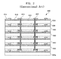
- FIG. 2 illustrates a conventional wafer-level chip stack package.
- at least one overlying wafer 610 and a single bottom wafer 610 a are stacked together using intermediate films 630 , typically a kind of anisotropic conductive film (ACF).
- ACF anisotropic conductive film
- Metal vias 617 are formed through the overlying wafers 610 , starting from an upper surface of the insulating layer 614 and extending to a lower surface of the wafers.
- Metal traces 615 connect the chip pads 612 to a top end of the corresponding metal vias 617 .
- the intermediate film 630 provides a connection between the bottom end of the metal vias 617 and the corresponding metal trace 615 arranged on the next lower overlying wafer 610 or the bottom wafer 610 a.
- wafer-level chip stacking processes as illustrated in FIG. 2 tend to suffer increased yield losses because a defective chip located on any of the included wafers 610 , 610 a will cause the chip-stack within which the defective chip is incorporated to fail.
- the failures caused by a single defective chip result in the lost of all of the properly functioning chips incorporated into the same chip stack.
- the number of properly functioning chips that will be lost, as well as the risk of incorporating a defective chip in a particular chip stack increases with the number of wafers being stacked.
- the exemplary embodiments of the present invention provide a variety of chip stack packages and methods for manufacturing such chip stack packages that are intended to reduce manufacturing time, manufacturing cost, and yield loss.
- a three-dimensional chip stack package comprises a common substrate, first and second chips, and a plurality of connection terminals.
- the substrate includes a first surface and a second surface.
- the first chip has parts of scribe lanes remaining after wafer sawing, and a plurality of first connection vias formed in the remaining parts of the scribe lanes and connecting upper and lower surfaces of the chip.
- the first chip is disposed on and electrically connected to the first surface of the substrate through the first connection vias.
- the second chip has parts of scribe lanes remaining after wafer sawing, and a plurality of second connection vias formed in the remaining parts of the scribe lanes and connecting upper and lower surfaces of the second chip.
- the second chip is disposed on and electrically connected to the upper surface of the first chip through the second connection vias.
- the connection terminals are disposed on the second surface of the substrate and electrically connected to the first connection vias of the first chip.
- the substrate on which the first and second chips are mounted may be a test wafer provided and configured for conducting wafer-level testing.
- the first and second chips are known-good dies that have passed required wafer-level tests.
- Each chip may also include a plurality of chip pads formed on the active or upper surface thereof and a plurality of rerouting lines connecting the chip pads to corresponding connection vias.
- the chip stack package may further comprise a plurality of first connection bumps provided between the substrate and the first chip and joined to the first connection vias, and a plurality of second connection bumps provided between the first and the second chips and joined to the first and second connection vias.
- the substrate and the first connection vias may also be directly joined and/or the first and second connection vias may be directly joined.
- the first and second connection bumps may be micro metal bumps, preferably having a diameter of about 20-60 ⁇ m.
- the lower surface of each chip may be, and typically is, formed by removing a majority the wafer thickness from the backside surface of the parent wafer.
- the thickness of each chip is no more than about 50 ⁇ m.
- each of the first and the second connection vias may be surrounded with an insulating layer.
- the first and second chips may have identical chip sizing and function, such as identical memory chips, or may have different chip sizing and/or chip function, such as a logic chip and a memory chip.
- An exemplary method according to the present invention provides a method for manufacturing such three-dimensional chip stack packages comprising providing at least two wafers each having a plurality of chips and scribe lanes between the adjacent chips; forming a plurality of via holes in both peripheral parts of each scribe lane; forming a plurality of connection vias by filling the via holes with metal; electrically connecting the connection vias to the chips; and partially removing the parent wafer material from a backside surface to expose lower surfaces of the connection vias are exposed on the backside surface.
- the exemplary method further comprises sawing the wafers along a central part of each scribe lane so that the individual chips are separated from each other while maintaining a peripheral part of each scribe lane with each of the separated chips; attaching the first separated chips to a test wafer so that the connection vias are electrically connected to the test wafer, and then performing wafer-level testing; attaching second separated chips on the first chips so that the connection vias of the second chips are electrically connected to the connection vias of the first chips, and then performing wafer-level testing; encapsulating the at least two-layered chips with a resin encapsulant; and separating individual chip stack packages by sawing the test wafer.
- the via holes are preferably formed in the scribe lines through a laser drilling process.
- additional via processing may include forming an insulating layer on the inner wall of each via hole, forming a barrier metal on the insulating layer, and forming a seed metal on the barrier metal.
- attaching the first chips to the test wafer may include providing first connection bumps on the test wafer, thermally joining the first connection bumps to the test wafer.
- attaching the second chips may include providing second connection bumps on the first chips and thermally joining the second connection bumps to the first chips. If both first and second connection bumps are utilized, it is preferred that the first connection bumps be formed from a material exhibiting a higher melting point than that of the material used to form the second connection bumps.
- the step of sawing the wafers is preferably accomplished using a laser cutter with the electrical connections between the connection vias and the chips preferably being accomplished through a rerouting technique.
- the step of removing a partial thickness of the parent wafer from the wafer backside is preferably accomplished by a spin-wet etching technique that may be used to reduce the thickness of the wafer to about 50 ⁇ m or less and may include forming a support layer on the backside surface of the thinned wafer.
- FIG. 1 is a cross-sectional view illustrating a conventional chip stack package manufactured at a chip level
- FIG. 2 is a cross-sectional view illustrating a conventional chip stack package manufactured at a wafer level
- FIG. 3 is a cross-sectional view illustrating a chip stack package in accordance with one embodiment of the present invention.
- FIG. 4 is a cross-sectional view schematically showing a chip stack package in accordance with another embodiment of the present invention.
- FIGS. 5 to 14 are cross-sectional views illustrating various steps according to an exemplary process for manufacturing chip stack packages in accordance an exemplary embodiment of the present invention.
- a chip stack package 100 includes two or more semiconductor chips 11 , 11 a stacked on a common substrate 31 .
- Each chip 11 , 11 a includes, at its peripheral regions, parts of scribe lanes S 1 and S 2 that remain after each of the wafers from which the chips are separated is sawed along the scribe lanes.
- Connection vias 19 are formed in the remaining part of each scribe lane S 1 and S 2 , for connecting the upper and lower surfaces of the chip 11 , 11 a .
- each of the connection vias 19 is preferably surrounded by a layer of a barrier metal 17 and an insulating layer 16 .
- Each of the connection vias 19 may also be connected to one or more corresponding chip pads 12 through a rerouting line 21 .
- connection bumps 35 may be provided between upper and lower connection vias 19 .
- other connection bumps 36 may be provided between the lowermost chip 11 a and the common substrate 31 .
- an alternative chip stack package 200 utilizes a direct joining between adjacent connection vias 119 of upper and lower chips 111 , 111 a and the lowermost chip 111 a and the common substrate 131 . Utilizing a direct joining technique may afford a reduction in the overall stack height of the resulting device.
- connection bumps 36 are micro metal bumps having a diameter of about 20-60 ⁇ m, whereas the connection terminals 45 are preferably solder balls having a diameter of about 120 ⁇ m.
- the common substrate 31 may be a wafer substrate obtained from a test wafer or otherwise provided with test device structures. During the manufacturing process, the chips 11 , 11 a may be mounted on the test wafer and subjected to both functional and parametric testing. Those chips that pass the defined testing protocol may then be provided as “known-good dies” or “known-good chips” for inclusion in the chip stack package 100 .
- the common substrate 31 may also comprise conventional printed circuit boards (PCB) or tape wiring boards. Further, one or more interposers or buffer layers may be incorporated into the chip stack 100 between adjacent chips 11 , 11 a and/or the common substrate.
- a chip stack package 100 may incorporate substantially identically sized semiconductor chips, e.g., using identical memory chips to increase memory density, but may also be configured for incorporating two or more chip sizes (not shown) if desired. In those instances in which the chip sizings are sufficiently different to prevent vertical alignment of the connection vias 19 , additional rerouting lines may be utilized to achieve the desired electrical connections.
- FIGS. 5-14 provide a sequence of cross-sectional views illustrating an exemplary process for manufacturing chip stack packages in accordance with an exemplary embodiment of the present invention. From the following description of the process, the structure of the above-discussed chip stack package will also be clear.
- a wafer 10 is processed using a conventional or non-conventional semiconductor fabrication process to form a plurality of individual semiconductor chips 11 on a front side surface of the wafer and typically has been subjected to at least preliminary electrical die sorting (EDS).
- EDS electrical die sorting
- the majority of the circuitry on each of the chips 11 will typically be covered with a passivation layer 13 that includes openings exposing a plurality of chip pads 12 .
- the wafer 10 also includes scribe lanes, scribe lines or kerfs, as indicated by a reference character ‘S’ in the drawing.
- the via holes 15 may be formed using any drilling or etching process capable of forming via holes having accurate placement, sizing and depth.
- Direct drilling techniques specifically laser drilling techniques, are, however preferred for their relative simplicity in contrast to plasma etching processes.
- Plasma etching techniques for example, require the formation of an etch mask, necessitating the formation of a pattern mask and a corresponding photolithography process for transferring the pattern mask to the wafer surface, complicating the manufacturing process, and may require other modification of the chip design.
- laser drilling requires no masking operation or complicated processing or modification of the existing chip design and may, therefore, be readily and simply incorporated into an existing wafer fabrication process. Laser drilling also provides the ability to modify the location, depth and sizing of the via holes without substantial difficulty.
- connection vias 19 are formed by filling the via holes 15 with a conductive material, typically a metal after forming an insulating layer 16 on the inner wall of the via holes by using a sputtering, chemical vapor deposition or other layer forming technique to prevent electrical contact between the connection via and the surrounding bulk material of the wafer 10 .
- a barrier metal layer 17 is then preferably formed on the insulating layer, typically by using a sputtering, evaporation or electroplating technique, to form a layer including titanium, titanium nitride, titanium-tungsten, platinum-silicon, aluminum or alloys thereof.
- a seed metal layer 18 is then preferably formed on the barrier metal layer 17 , followed by the deposition or formation of the primary conductive material to fill the remainder of via hole 15 and complete the connection via 19 .
- the primary conductive material may be deposited in the via hole 15 using an electroplating process to deposit a metal such as copper, gold or tungsten
- connection vias 19 may be connected to corresponding chip pads 12 by utilizing the rerouting technique, also referred to as the redistribution technique.
- a metal layer may be deposited on the surface of wafer 10 to make contact with both a chip pad 12 and a corresponding connection via 19 and then patterned using a conventional technique, such as resist lift off or a metal etch to form rerouting lines 21 .
- the rerouting lines 21 can be formed simultaneously during the formation of the connection vias 19 .
- a cover layer 23 may be formed to protect the rerouting lines 21 and portions of the connection vias 19 from the environment.
- an optional support layer 25 including openings for exposing the lower surfaces of the connection vias 19 may be formed on the backside of the wafer using an insulating material or materials.
- the support layer 25 is preferably selected to improve the strength and/or handling characteristics of the wafer 10 and also to reduce the likelihood that the thinned wafer will warp.
- the support layer pattern 25 may be temporary or permanent, with adhesive tapes and polyimide films being useful as temporary support layer patterns.
- the wafer 10 is separated into its individual chips by cutting or sawing through a central region of the scribe lanes S of the thinned wafer using a cutting implement 29 .
- the sawing operation is conducted so as not to damage or expose the connection vias 19 disposed in the opposed peripheral regions S 1 and S 2 of each scribe lane S.
- each of the separated chips 11 will include, along its periphery, a plurality of connection vias 19 in the remaining peripheral region S 1 , S 2 of the scribe lane S.
- the sawing operation is preferably controlled to limit or avoid removal or the support layer 25 , allowing the support layer to maintain, at least temporarily, the relative orientation of the separated chips 11 .
- the sawing operation may utilize a range of cutting or dicing implements 29 , laser cutters are preferred for reducing damage to the wafer 10 , such as chipping or cracking, and for reducing the width of the material removed from the scribe lanes S.
- connection bumps 36 are utilized to physically attach and electrically connect the chips 11 a to the test wafer 30 , as illustrated in FIG. 4 , direct connection between the chips and the test wafer may also be utilized.
- connection bumps 36 may be arranged on the test wafer 30 at positions, sometimes referred to as ball pads or ball lands, corresponding to the connection vias 19 in the chips 11 a.
- connection vias 19 are connected to the test wafer 30 , typically by using a thermal process to reflow or otherwise establish an electrical and physical connection between the connection vias 19 and corresponding contacts on the test wafer, package-level testing may be performed by exercising the chips 11 a with an external tester (not shown) and evaluating the performance of the chips. Any of the chips 11 a that fail the testing may be removed from the test wafer 30 and replaced with another chip, that will then be subjected to the testing procedure.
- connection bumps 35 may be formed or provided on the upper portions of the connection vias 19 of the lowermost chips 11 a for attaching the second layer chips 11 .
- the connection vias 19 of the second layer chips 11 may then be thermally joined to the connection bumps 35 on the lowermost chips.
- the second layer chips 11 may be subjected to functional and/or parametric testing. As with the lowermost chips 11 a , those second layer chips 11 that fail the testing may be replaced with another chip that is then tested until all the second layer chips are passing the test procedure. Again, as illustrated in FIG. 4 , the second and other subsequent layers of chips 11 may, in the alternative, be attached directly to the underlying chips 11 a , 11 without the use of connection bumps.
- This basic chip-stacking process may be repeated for each subsequent layer of chips 11 .
- this stacking process provides chip stacks of known-good dies for use in chip stack packages.
- failing chips 11 , 11 a are removed and replaced with another chip during each chip-stacking step.
- a sufficient quantity of heat should be applied to melt the connection bumps that support the failing chips and allow such chips to be removed from the layer without altering the connection and configuration of adjacent and/or underlying chips.
- Such a result may be achieved by selecting materials for use in the connection bumps 35 , 36 that have successively lower melting points for each successive layer of chips 11 applied to the test wafer 30 . In this way, chips 11 included in the most recently layer applied layer can be removed without affecting the known-good dies in the underlying layer(s).
- the size of the conductive bumps 35 , 36 should be selected to generally correspond to the sizing of the connection vias 19 and may exhibit typical sizing of about 20-60 ⁇ m.
- the connection bumps 35 , 36 may be formed using any conventional technique, such as ball injection or screen printing, that can achieve the desired sizing and placement accuracy.
- the stacked and tested chips 11 a , 11 and a portion of the test wafer 30 may be encapsulated with a resin encapsulant 41 at a wafer level. Because this encapsulating process is performed in one operation on the test wafer 30 , it may provide a reduction in the process time as compared with chip-level encapsulation of a corresponding chip stack structure. Depending on the spacing between adjacent chips 11 a , 11 in the same level of the chip stack structure, the resin encapsulant may completely fill the space between adjacent chip stack structures (not shown) or a mold may be utilized to isolate the chip stack structures during the encapsulation process and leave an open space between adjacent chip stack structures.
- the multi-layer structure may be sawed by sawing through the encapsulating material 41 between the stacks of chips 11 a , 11 (if present) and/or through the test wafer 30 , to separate the individual chip stack packages 100 from each other.
- solder balls 45 may be formed on or applied to the lower surface of vias 33 on the lower surface of the test wafer 30 , which corresponds to the common substrate 31 of FIG. 3 , to provide external connections for mounting and electrically connecting the chip stack package on a PCB or other substrate.
Landscapes
- Engineering & Computer Science (AREA)
- Microelectronics & Electronic Packaging (AREA)
- Power Engineering (AREA)
- Computer Hardware Design (AREA)
- Physics & Mathematics (AREA)
- Condensed Matter Physics & Semiconductors (AREA)
- General Physics & Mathematics (AREA)
- Manufacturing & Machinery (AREA)
- Internal Circuitry In Semiconductor Integrated Circuit Devices (AREA)
- Testing Or Measuring Of Semiconductors Or The Like (AREA)
Abstract
A method for manufacturing chip stack packages may include: providing at least two wafers, each wafer having a plurality of chips, and scribe lanes formed between and separating adjacent chips; forming a plurality of via holes in peripheral portions of the scribe lanes; forming connection vias by filling the via holes; establishing electrical connections between the chip pads and corresponding connection vias; removing material from the back sides of the wafers to form thinned wafers; separating the thinned wafers into individual chips by removing a central portion of each scribe lane; attaching a first plurality of individual chips to a test wafer; attaching a second plurality of individual chips to the first plurality of individual chips to form a plurality of chip stack structures; encapsulating the plurality of chip stack structures; and separating the plurality of chip stack structures to form individual chip stack packages.
Description
This application claims priority from and is a Continuation of U.S. patent application Ser. No. 12/385,855, filed on Apr. 22, 2009 now U.S. Pat. No. 7,977,156, which is a Continuation of U.S. patent application Ser. No. 11/889,400, filed on Aug. 13, 2007 (now U.S. Pat. No. 7,537,959), which is a divisional of U.S. patent application Ser. No. 10/890,995, filed on Jul. 15, 2004 (now U.S. Pat. No. 7,276,799) the entire contents of all of which are incorporated herein by reference.
1. Field
The present invention relates generally to electronic packaging technology and, more particularly, to a three-dimensional multi-chip stack package and a method for manufacturing such chip stack packages.
2. Description of the Related Art
With the rapid advancement of very large scale integrated circuit (VLSI) technologies, traditional packaging is becoming a performance bottleneck of the advanced microelectronics devices. This is due to the rapidly increasing of pin count and clock speed on the advanced devices. Along with the fast clock speed, power distribution of the advanced devices also is an important issue that must be addressed. Furthermore, the chip size of the advanced devices continues to grow although sub-micron processing technologies continue to reduce the minimum feature sizes on the devices. Multi-chip packaging technology is a packaging technique that has been developed to address some of the problems associated with conventional single-chip packaging.
A three-dimensional chip stack packaging has been introduced as part of the multi-chip packaging. FIG. 1 illustrates a conventional chip stack package 500 that includes two chips 511, 513 stacked on a common substrate 520. Specifically, a lower chip 511 is attached through an adhesive layer 531 on the substrate 520 so that an active surface, on which chip pads 512 are formed, faces away from the substrate (upward). An upper chip 513, which includes an active surface having chip pads 514, is attached to the active surface of the lower chip 511 using an adhesive layer 533 so that chip pads 514 face upward. Bonding wires 541, 543 are then used to form electrical connection between the chip pads 512, 514 of the chips 511, 513 and the substrate 520. An encapsulating body 550 is then formed to surround and protect the chips 511 and 513, the wires 541 and 543, and at least a portion of the top surface of the substrate 520 from the environment. A series of solder balls 560 are formed on a bottom surface of the substrate 520 to provide external electrical connections for the chips 511, 513.
Relative to single chip packaging, however, such conventional multi-chip stack packaging methods, however, tend to incur increased manufacturing time and cost associated with stacking the individual chips. In order to avoid these issues, wafer-level chip stacking has been considered to be an option for three-dimensional packaging. The ability to stack and connect multiple chips, before separating the individual chips from their parent wafers, offers several benefits over conventional chip stacking techniques including reduced manufacturing time and reduced cost
Unfortunately, wafer-level chip stacking processes as illustrated in FIG. 2 tend to suffer increased yield losses because a defective chip located on any of the included wafers 610, 610 a will cause the chip-stack within which the defective chip is incorporated to fail. The failures caused by a single defective chip result in the lost of all of the properly functioning chips incorporated into the same chip stack. The number of properly functioning chips that will be lost, as well as the risk of incorporating a defective chip in a particular chip stack, increases with the number of wafers being stacked.
The exemplary embodiments of the present invention provide a variety of chip stack packages and methods for manufacturing such chip stack packages that are intended to reduce manufacturing time, manufacturing cost, and yield loss.
In an exemplary embodiment of the present invention, a three-dimensional chip stack package comprises a common substrate, first and second chips, and a plurality of connection terminals. The substrate includes a first surface and a second surface. The first chip has parts of scribe lanes remaining after wafer sawing, and a plurality of first connection vias formed in the remaining parts of the scribe lanes and connecting upper and lower surfaces of the chip. The first chip is disposed on and electrically connected to the first surface of the substrate through the first connection vias. The second chip has parts of scribe lanes remaining after wafer sawing, and a plurality of second connection vias formed in the remaining parts of the scribe lanes and connecting upper and lower surfaces of the second chip. The second chip is disposed on and electrically connected to the upper surface of the first chip through the second connection vias. The connection terminals are disposed on the second surface of the substrate and electrically connected to the first connection vias of the first chip.
In the chip stack package according to the invention, the substrate on which the first and second chips are mounted may be a test wafer provided and configured for conducting wafer-level testing. Preferably, the first and second chips are known-good dies that have passed required wafer-level tests. Each chip may also include a plurality of chip pads formed on the active or upper surface thereof and a plurality of rerouting lines connecting the chip pads to corresponding connection vias.
The chip stack package may further comprise a plurality of first connection bumps provided between the substrate and the first chip and joined to the first connection vias, and a plurality of second connection bumps provided between the first and the second chips and joined to the first and second connection vias. The substrate and the first connection vias may also be directly joined and/or the first and second connection vias may be directly joined.
If utilized, the first and second connection bumps may be micro metal bumps, preferably having a diameter of about 20-60 μm. Furthermore, the lower surface of each chip may be, and typically is, formed by removing a majority the wafer thickness from the backside surface of the parent wafer. Preferably, the thickness of each chip is no more than about 50 μm. Further, each of the first and the second connection vias may be surrounded with an insulating layer. The first and second chips may have identical chip sizing and function, such as identical memory chips, or may have different chip sizing and/or chip function, such as a logic chip and a memory chip.
An exemplary method according to the present invention provides a method for manufacturing such three-dimensional chip stack packages comprising providing at least two wafers each having a plurality of chips and scribe lanes between the adjacent chips; forming a plurality of via holes in both peripheral parts of each scribe lane; forming a plurality of connection vias by filling the via holes with metal; electrically connecting the connection vias to the chips; and partially removing the parent wafer material from a backside surface to expose lower surfaces of the connection vias are exposed on the backside surface. The exemplary method further comprises sawing the wafers along a central part of each scribe lane so that the individual chips are separated from each other while maintaining a peripheral part of each scribe lane with each of the separated chips; attaching the first separated chips to a test wafer so that the connection vias are electrically connected to the test wafer, and then performing wafer-level testing; attaching second separated chips on the first chips so that the connection vias of the second chips are electrically connected to the connection vias of the first chips, and then performing wafer-level testing; encapsulating the at least two-layered chips with a resin encapsulant; and separating individual chip stack packages by sawing the test wafer.
In the exemplary method, the via holes are preferably formed in the scribe lines through a laser drilling process. After forming the initial via hole, additional via processing may include forming an insulating layer on the inner wall of each via hole, forming a barrier metal on the insulating layer, and forming a seed metal on the barrier metal. Also, attaching the first chips to the test wafer may include providing first connection bumps on the test wafer, thermally joining the first connection bumps to the test wafer. Similarly, attaching the second chips may include providing second connection bumps on the first chips and thermally joining the second connection bumps to the first chips. If both first and second connection bumps are utilized, it is preferred that the first connection bumps be formed from a material exhibiting a higher melting point than that of the material used to form the second connection bumps.
Further, the step of sawing the wafers is preferably accomplished using a laser cutter with the electrical connections between the connection vias and the chips preferably being accomplished through a rerouting technique. Further, the step of removing a partial thickness of the parent wafer from the wafer backside is preferably accomplished by a spin-wet etching technique that may be used to reduce the thickness of the wafer to about 50 μm or less and may include forming a support layer on the backside surface of the thinned wafer.
These and other objects, features and advantages of the present invention will be readily understood with reference to the following detailed description thereof provided in conjunction with the accompanying drawings, wherein the same reference numerals are used designate identical and/or corresponding structural elements and features, and, in which:
These drawings are provided for illustrative purposes only and are not drawn to scale. The spatial relationships and relative sizing of the elements illustrated in the various embodiments may have been reduced, expanded or rearranged to improve the clarity of the figure with respect to the corresponding description. The figures, therefore, should not be interpreted as accurately reflecting the relative sizing or positioning of the corresponding structural elements that could be encompassed by an actual device manufactured according to the exemplary embodiments of the invention.
The present invention will now be described more fully hereinafter with reference to the accompanying drawings, in which several exemplary embodiments of the invention are illustrated. This invention may, however, be embodied in many different forms and should not be construed as limited to the particular embodiments set forth herein. Rather, these embodiments are provided so that this disclosure will be thorough and complete, and will fully convey the scope of the invention to those skilled in the art.
In the description, well-known structures and processes have not been described or illustrated in detail to avoid obscuring the present invention. It will be appreciated that for simplicity and clarity of illustration, some elements illustrated in the figures have not necessarily been drawn to scale. For example, the dimensions of some of the elements have been exaggerated or reduced relative to other elements for clarity.
As illustrated in FIG. 3 a chip stack package 100 according to an exemplary embodiment of the present invention includes two or more semiconductor chips 11, 11 a stacked on a common substrate 31. Each chip 11, 11 a includes, at its peripheral regions, parts of scribe lanes S1 and S2 that remain after each of the wafers from which the chips are separated is sawed along the scribe lanes. Connection vias 19 are formed in the remaining part of each scribe lane S1 and S2, for connecting the upper and lower surfaces of the chip 11, 11 a. In order to improve the electrical properties, each of the connection vias 19 is preferably surrounded by a layer of a barrier metal 17 and an insulating layer 16. Each of the connection vias 19 may also be connected to one or more corresponding chip pads 12 through a rerouting line 21.
To establish a stack and electrical interconnection between adjacent chips 11, 11 a, connection bumps 35 may be provided between upper and lower connection vias 19. Similarly, other connection bumps 36 may be provided between the lowermost chip 11 a and the common substrate 31.
It is also possible to join adjacent chips directly and join the lowermost chip directly to the common substrate 31. As illustrated in FIG. 4 , an alternative chip stack package 200 utilizes a direct joining between adjacent connection vias 119 of upper and lower chips 111, 111 a and the lowermost chip 111 a and the common substrate 131. Utilizing a direct joining technique may afford a reduction in the overall stack height of the resulting device.
Again referencing FIG. 3 , the electrical interconnection between the stacked chips 11, the lowermost chip 11 a and the substrate 31 is established through the connection vias 19 and the connection bumps 35, 36. Further, the common substrate 31 provides an electrical path, e.g. through vias 33, between the connection bumps 36 joined to the connection vias 19 of the lowermost chip 11 a and connection terminals 45 disposed on the common substrate opposite the chips. Preferably, the connection bumps 36 are micro metal bumps having a diameter of about 20-60 μm, whereas the connection terminals 45 are preferably solder balls having a diameter of about 120 μm.
The common substrate 31 may be a wafer substrate obtained from a test wafer or otherwise provided with test device structures. During the manufacturing process, the chips 11, 11 a may be mounted on the test wafer and subjected to both functional and parametric testing. Those chips that pass the defined testing protocol may then be provided as “known-good dies” or “known-good chips” for inclusion in the chip stack package 100. The common substrate 31 may also comprise conventional printed circuit boards (PCB) or tape wiring boards. Further, one or more interposers or buffer layers may be incorporated into the chip stack 100 between adjacent chips 11, 11 a and/or the common substrate.
A chip stack package 100 may incorporate substantially identically sized semiconductor chips, e.g., using identical memory chips to increase memory density, but may also be configured for incorporating two or more chip sizes (not shown) if desired. In those instances in which the chip sizings are sufficiently different to prevent vertical alignment of the connection vias 19, additional rerouting lines may be utilized to achieve the desired electrical connections.
As illustrated in FIG. 5 , a wafer 10 is processed using a conventional or non-conventional semiconductor fabrication process to form a plurality of individual semiconductor chips 11 on a front side surface of the wafer and typically has been subjected to at least preliminary electrical die sorting (EDS). The majority of the circuitry on each of the chips 11 will typically be covered with a passivation layer 13 that includes openings exposing a plurality of chip pads 12. Between adjacent chips 11, the wafer 10 also includes scribe lanes, scribe lines or kerfs, as indicated by a reference character ‘S’ in the drawing.
A plurality of via holes 15 are then formed in the scribe lane adjacent each of the chips 11 separated by the scribe lane, with the via holes 14 associated with each of the chips 11 being separated by a intermediate portion of the scribe lane S. Although the actually sizing may vary depending on the type of wafer 10, the type of device 11 and the manufacturing tolerance of the semiconductor manufacturing process utilized, the scribe lanes S may have a typical width of about 110-220 μm. The via holes 15 are preferably sized and positioned within the scribe lane S to allow the separation operation, typically a laser cutter or saw blade, to remove a central region, typically between about 20-40 μm, from the intermediate portion of the scribe line S without exposing any portion of the via holes.
The via holes 15 may be formed using any drilling or etching process capable of forming via holes having accurate placement, sizing and depth. Direct drilling techniques, specifically laser drilling techniques, are, however preferred for their relative simplicity in contrast to plasma etching processes. Plasma etching techniques, for example, require the formation of an etch mask, necessitating the formation of a pattern mask and a corresponding photolithography process for transferring the pattern mask to the wafer surface, complicating the manufacturing process, and may require other modification of the chip design. On the other hand, laser drilling requires no masking operation or complicated processing or modification of the existing chip design and may, therefore, be readily and simply incorporated into an existing wafer fabrication process. Laser drilling also provides the ability to modify the location, depth and sizing of the via holes without substantial difficulty.
Next, as shown in FIG. 6 , a plurality of connection vias 19 are formed by filling the via holes 15 with a conductive material, typically a metal after forming an insulating layer 16 on the inner wall of the via holes by using a sputtering, chemical vapor deposition or other layer forming technique to prevent electrical contact between the connection via and the surrounding bulk material of the wafer 10. A barrier metal layer 17 is then preferably formed on the insulating layer, typically by using a sputtering, evaporation or electroplating technique, to form a layer including titanium, titanium nitride, titanium-tungsten, platinum-silicon, aluminum or alloys thereof. A seed metal layer 18 is then preferably formed on the barrier metal layer 17, followed by the deposition or formation of the primary conductive material to fill the remainder of via hole 15 and complete the connection via 19. The primary conductive material may be deposited in the via hole 15 using an electroplating process to deposit a metal such as copper, gold or tungsten
As illustrated in FIG. 7 , the connection vias 19 may be connected to corresponding chip pads 12 by utilizing the rerouting technique, also referred to as the redistribution technique. Specifically, a metal layer may be deposited on the surface of wafer 10 to make contact with both a chip pad 12 and a corresponding connection via 19 and then patterned using a conventional technique, such as resist lift off or a metal etch to form rerouting lines 21. The rerouting lines 21 can be formed simultaneously during the formation of the connection vias 19. After forming the rerouting lines 21, a cover layer 23 may be formed to protect the rerouting lines 21 and portions of the connection vias 19 from the environment.
Next, as shown in FIG. 8 , a portion of the wafer 10 thickness is removed from the backside of the wafer, typically by using a chemical-mechanical polishing (CMP) or a spin-wet etching technique. In accord with the exemplary embodiments of the present invention, the portion of the wafer 10 thickness removed will be sufficient to expose a lower portion of the connection vias 19. The spin-wet etching technique in particular has been found capable of achieving wafer 10 thicknesses of 50 μm or less without inflicting undue mechanical damage to the wafer 10.
As illustrated in FIG. 9 , after thinning the wafer 10, an optional support layer 25 including openings for exposing the lower surfaces of the connection vias 19 may be formed on the backside of the wafer using an insulating material or materials. When present, the support layer 25 is preferably selected to improve the strength and/or handling characteristics of the wafer 10 and also to reduce the likelihood that the thinned wafer will warp. The support layer pattern 25 may be temporary or permanent, with adhesive tapes and polyimide films being useful as temporary support layer patterns.
Next, as illustrated in FIG. 10 , the wafer 10 is separated into its individual chips by cutting or sawing through a central region of the scribe lanes S of the thinned wafer using a cutting implement 29. The sawing operation is conducted so as not to damage or expose the connection vias 19 disposed in the opposed peripheral regions S1 and S2 of each scribe lane S. Thus, after the sawing operation is completed, each of the separated chips 11 will include, along its periphery, a plurality of connection vias 19 in the remaining peripheral region S1, S2 of the scribe lane S. The sawing operation is preferably controlled to limit or avoid removal or the support layer 25, allowing the support layer to maintain, at least temporarily, the relative orientation of the separated chips 11. Although the sawing operation may utilize a range of cutting or dicing implements 29, laser cutters are preferred for reducing damage to the wafer 10, such as chipping or cracking, and for reducing the width of the material removed from the scribe lanes S.
Next, as illustrated in FIG. 11 , the separated chips 11 a, which will act as the lowermost chips in a chip stack package, may be removed from the support layer 25 and attached to a test wafer 30. The test wafer 30 is, in turn, electrically coupled to external testers (not shown) and that are used to apply desired electrical and/or functional tests to the chips 11 a. Although, as illustrated in FIG. 11 , connection bumps 36 are utilized to physically attach and electrically connect the chips 11 a to the test wafer 30, as illustrated in FIG. 4 , direct connection between the chips and the test wafer may also be utilized. When connection bumps 36 are utilized, they may be arranged on the test wafer 30 at positions, sometimes referred to as ball pads or ball lands, corresponding to the connection vias 19 in the chips 11 a.
After the connection vias 19 are connected to the test wafer 30, typically by using a thermal process to reflow or otherwise establish an electrical and physical connection between the connection vias 19 and corresponding contacts on the test wafer, package-level testing may be performed by exercising the chips 11 a with an external tester (not shown) and evaluating the performance of the chips. Any of the chips 11 a that fail the testing may be removed from the test wafer 30 and replaced with another chip, that will then be subjected to the testing procedure.
After the functioning of each of the lowermost chips 11 a provided on the test wafer has been verified, the first layer of overlaying chips 11, i.e., second layer chips, are provided on the lowermost chips, as shown in FIG. 12 . Connection bumps 35 may be formed or provided on the upper portions of the connection vias 19 of the lowermost chips 11 a for attaching the second layer chips 11. The connection vias 19 of the second layer chips 11 may then be thermally joined to the connection bumps 35 on the lowermost chips.
Once the second layer chips 11 have been attached to the lowermost chips 11 a, the second layer chips 11 may be subjected to functional and/or parametric testing. As with the lowermost chips 11 a, those second layer chips 11 that fail the testing may be replaced with another chip that is then tested until all the second layer chips are passing the test procedure. Again, as illustrated in FIG. 4 , the second and other subsequent layers of chips 11 may, in the alternative, be attached directly to the underlying chips 11 a, 11 without the use of connection bumps.
This basic chip-stacking process may be repeated for each subsequent layer of chips 11. By ensuring that all of the chips 11 arranged in a single layer pass the tests before the next layer of chips 11 are applied, this stacking process provides chip stacks of known-good dies for use in chip stack packages.
As discussed above, failing chips 11, 11 a are removed and replaced with another chip during each chip-stacking step. In order to remove the failing chips 11, 11 a, a sufficient quantity of heat should be applied to melt the connection bumps that support the failing chips and allow such chips to be removed from the layer without altering the connection and configuration of adjacent and/or underlying chips. Such a result may be achieved by selecting materials for use in the connection bumps 35, 36 that have successively lower melting points for each successive layer of chips 11 applied to the test wafer 30. In this way, chips 11 included in the most recently layer applied layer can be removed without affecting the known-good dies in the underlying layer(s).
The size of the conductive bumps 35, 36 should be selected to generally correspond to the sizing of the connection vias 19 and may exhibit typical sizing of about 20-60 μm. The connection bumps 35, 36 may be formed using any conventional technique, such as ball injection or screen printing, that can achieve the desired sizing and placement accuracy.
Next, as illustrated in FIG. 13 , the stacked and tested chips 11 a, 11 and a portion of the test wafer 30 may be encapsulated with a resin encapsulant 41 at a wafer level. Because this encapsulating process is performed in one operation on the test wafer 30, it may provide a reduction in the process time as compared with chip-level encapsulation of a corresponding chip stack structure. Depending on the spacing between adjacent chips 11 a, 11 in the same level of the chip stack structure, the resin encapsulant may completely fill the space between adjacent chip stack structures (not shown) or a mold may be utilized to isolate the chip stack structures during the encapsulation process and leave an open space between adjacent chip stack structures.
Next, as illustrated in FIG. 14 , the multi-layer structure may be sawed by sawing through the encapsulating material 41 between the stacks of chips 11 a, 11 (if present) and/or through the test wafer 30, to separate the individual chip stack packages 100 from each other. Then, as illustrated in FIG. 3 , solder balls 45 may be formed on or applied to the lower surface of vias 33 on the lower surface of the test wafer 30, which corresponds to the common substrate 31 of FIG. 3 , to provide external connections for mounting and electrically connecting the chip stack package on a PCB or other substrate.
While this invention has been particularly shown and described with reference to preferred embodiments thereof, it will be understood by those skilled in the art that various changes in form and details may be made therein without departing from the spirit and scope of the invention as defined by the appended claims.
Claims (19)
1. A chip stack package comprising:
a package substrate including:
a first surface, the first surface including at least a first terminal; and
a second surface, the second surface including at least a second terminal, the second terminal being in electrical contact with the first terminal,
wherein the second terminal is an external terminal of the package; and
a first chip stacked on the package substrate, the first chip being a lowermost chip of the chip stack package, the first chip including:
a first surface;
a second surface;
at least a first chip pad on the first surface of the first chip;
at least a first connection via formed through a portion of the first chip and separate from the first chip pad, the first connection via having an upper surface and a lower surface; and
at least a first rerouting line connecting the first chip pad and the first connection via,
wherein the package substrate is a wafer substrate having a size bigger than a size of the first chip.
2. A chip stack package according to claim 1 , wherein the first terminal is a connection bump directly connected to the lower surface of the first connection via.
3. A chip stack package according to claim 1 , wherein the second surface of the chip faces the first surface of the package substrate, and the first terminal is a bump arranged between the second surface of the chip and the first surface of the package substrate.
4. A chip stack package according to claim 1 , further comprising:
a second chip stacked on the first chip, the second chip including:
a backside surface;
an active surface;
a second chip pad on the active surface;
a second connection via formed through a portion of the second chip separate from the second chip pad, the second connection via having an upper surface and a lower surface; and
a second rerouting line connecting the second chip pad to the second connection via,
wherein the second connection via is electrically connected to the first connection via.
5. A chip stack package according to claim 4 , further comprising:
a third terminal, the third terminal being arranged between the lower surface of the second connection via and the upper surface of the first connection via.
6. A chip stack package according to claim 5 , wherein the third terminal is a bump directly connected to the lower surface of the second connection via and the upper surface of the first connection via.
7. A chip stack package according to claim 5 , wherein the first and third terminals are micro metal bumps.
8. A chip stack package according to claim 4 , wherein the first and second chips are memory chips and have substantially identical dimensions.
9. A chip stack package according to claim 4 , wherein the lower surface of the second connection via is directly connected to the upper surface of the first connection via.
10. A chip stack package according to claim 1 , wherein the first terminal is connected to the second terminal through a package substrate via that passes through the package substrate.
11. The chip stack package according to claim 10 , wherein the first terminal is a solder ball and the second terminal is a bump.
12. The chip stack package according to claim 10 , wherein the package substrate via is vertically aligned with the first connection via.
13. The chip stack package according to claim 1 , wherein:
the first connection via is laterally separate from the first chip pad;
the first rerouting line is disposed on the first surface of the first chip; and
the lower surface of the first connection via is vertically aligned with the first terminal.
14. The chip stack package according to claim 1 , wherein the first rerouting line comprises a conductive material formed in a straight pattern on the first surface of the first chip.
15. A chip stack package comprising:
a first chip including:
a first backside surface;
a first active surface;
at least a first chip pad on the active surface;
at least a first connection via formed through a portion of the first chip and separate from the first chip pad, the first connection via having an upper surface and a lower surface, a lower portion of the first connection via extending beyond the first backside surface; and
at least a first rerouting line connecting the first chip pad and the first connection via;
a second chip stacked on the first chip, the second chip including:
a second backside surface;
an second active surface;
a second chip pad on the active surface;
a second connection via formed through a portion of the second chip separate from the second chip pad, the second connection via having an upper surface and a lower surface, a lower portion of the first connection via extending beyond the second backside surface; and
a second rerouting line connecting the second chip pad and the second connection via;
a wafer substrate mounting the first chip and the second chip, the wafer substrate being a package substrate of the chip stack package, and the first chip being a lowermost chip of the chip stack package,
wherein a size of the wafer substrate is bigger than a size of the first chip.
16. A chip stack package according to claim 15 , wherein the first and second chips are memory chips and have substantially identical dimensions.
17. A chip stack package according to claim 15 , wherein:
the first connection via is laterally separate from the first chip pad;
the first rerouting line is disposed on the first active surface of the first chip;
the second connection via is laterally separate from the second chip pad; and
the second rerouting line is disposed on the second active surface.
18. The chip stack package according to claim 17 , wherein:
the second connection via is vertically aligned with the first connection via; and
the lower surface of the second connection via is directly connected to the upper surface of the first connection via.
19. The chip stack package according to claim 15 , wherein the first rerouting line comprises a conductive material formed in a straight pattern on the first active surface of the first chip, and the second rerouting line comprises a conductive material formed in a straight pattern on the second active surface of the second chip.
Priority Applications (1)
| Application Number | Priority Date | Filing Date | Title |
|---|---|---|---|
| US13/154,165 US8368231B2 (en) | 2003-08-26 | 2011-06-06 | Chipstack package and manufacturing method thereof |
Applications Claiming Priority (6)
| Application Number | Priority Date | Filing Date | Title |
|---|---|---|---|
| KR2003-59166 | 2003-08-26 | ||
| KR10-2003-0059166A KR100537892B1 (en) | 2003-08-26 | 2003-08-26 | Chip stack package and manufacturing method thereof |
| US10/890,995 US7276799B2 (en) | 2003-08-26 | 2004-07-15 | Chip stack package and manufacturing method thereof |
| US11/889,400 US7537959B2 (en) | 2003-08-26 | 2007-08-13 | Chip stack package and manufacturing method thereof |
| US12/385,855 US7977156B2 (en) | 2003-08-26 | 2009-04-22 | Chipstack package and manufacturing method thereof |
| US13/154,165 US8368231B2 (en) | 2003-08-26 | 2011-06-06 | Chipstack package and manufacturing method thereof |
Related Parent Applications (1)
| Application Number | Title | Priority Date | Filing Date |
|---|---|---|---|
| US12/385,855 Continuation US7977156B2 (en) | 2003-08-26 | 2009-04-22 | Chipstack package and manufacturing method thereof |
Publications (2)
| Publication Number | Publication Date |
|---|---|
| US20110237004A1 US20110237004A1 (en) | 2011-09-29 |
| US8368231B2 true US8368231B2 (en) | 2013-02-05 |
Family
ID=34214705
Family Applications (4)
| Application Number | Title | Priority Date | Filing Date |
|---|---|---|---|
| US10/890,995 Active 2025-03-04 US7276799B2 (en) | 2003-08-26 | 2004-07-15 | Chip stack package and manufacturing method thereof |
| US11/889,400 Active 2024-10-13 US7537959B2 (en) | 2003-08-26 | 2007-08-13 | Chip stack package and manufacturing method thereof |
| US12/385,855 Expired - Lifetime US7977156B2 (en) | 2003-08-26 | 2009-04-22 | Chipstack package and manufacturing method thereof |
| US13/154,165 Expired - Lifetime US8368231B2 (en) | 2003-08-26 | 2011-06-06 | Chipstack package and manufacturing method thereof |
Family Applications Before (3)
| Application Number | Title | Priority Date | Filing Date |
|---|---|---|---|
| US10/890,995 Active 2025-03-04 US7276799B2 (en) | 2003-08-26 | 2004-07-15 | Chip stack package and manufacturing method thereof |
| US11/889,400 Active 2024-10-13 US7537959B2 (en) | 2003-08-26 | 2007-08-13 | Chip stack package and manufacturing method thereof |
| US12/385,855 Expired - Lifetime US7977156B2 (en) | 2003-08-26 | 2009-04-22 | Chipstack package and manufacturing method thereof |
Country Status (3)
| Country | Link |
|---|---|
| US (4) | US7276799B2 (en) |
| JP (1) | JP4602715B2 (en) |
| KR (1) | KR100537892B1 (en) |
Cited By (4)
| Publication number | Priority date | Publication date | Assignee | Title |
|---|---|---|---|---|
| US9397034B2 (en) | 2006-08-08 | 2016-07-19 | Samsung Electronics Co., Ltd. | Multi-chip package having a stacked plurality of different sized semiconductor chips, and method of manufacturing the same |
| US9673183B2 (en) * | 2015-07-07 | 2017-06-06 | Micron Technology, Inc. | Methods of making semiconductor device packages and related semiconductor device packages |
| US10083939B2 (en) | 2016-05-17 | 2018-09-25 | Samsung Electronics Co., Ltd. | Semiconductor package |
| US11302572B2 (en) | 2019-12-27 | 2022-04-12 | Samsung Electronics Co., Ltd. | Semiconductor package and method of manufacturing the same |
Families Citing this family (435)
| Publication number | Priority date | Publication date | Assignee | Title |
|---|---|---|---|---|
| US6930256B1 (en) | 2002-05-01 | 2005-08-16 | Amkor Technology, Inc. | Integrated circuit substrate having laser-embedded conductive patterns and method therefor |
| US9691635B1 (en) | 2002-05-01 | 2017-06-27 | Amkor Technology, Inc. | Buildup dielectric layer having metallization pattern semiconductor package fabrication method |
| US7633765B1 (en) | 2004-03-23 | 2009-12-15 | Amkor Technology, Inc. | Semiconductor package including a top-surface metal layer for implementing circuit features |
| US7548430B1 (en) | 2002-05-01 | 2009-06-16 | Amkor Technology, Inc. | Buildup dielectric and metallization process and semiconductor package |
| JP2005051150A (en) * | 2003-07-31 | 2005-02-24 | Seiko Epson Corp | Semiconductor device, its manufacturing method, circuit board, and electronic apparatus |
| KR100537892B1 (en) | 2003-08-26 | 2005-12-21 | 삼성전자주식회사 | Chip stack package and manufacturing method thereof |
| JP4340517B2 (en) | 2003-10-30 | 2009-10-07 | Okiセミコンダクタ株式会社 | Semiconductor device and manufacturing method thereof |
| US8084866B2 (en) | 2003-12-10 | 2011-12-27 | Micron Technology, Inc. | Microelectronic devices and methods for filling vias in microelectronic devices |
| US7091124B2 (en) * | 2003-11-13 | 2006-08-15 | Micron Technology, Inc. | Methods for forming vias in microelectronic devices, and methods for packaging microelectronic devices |
| US11081370B2 (en) | 2004-03-23 | 2021-08-03 | Amkor Technology Singapore Holding Pte. Ltd. | Methods of manufacturing an encapsulated semiconductor device |
| US10811277B2 (en) | 2004-03-23 | 2020-10-20 | Amkor Technology, Inc. | Encapsulated semiconductor package |
| US20050247894A1 (en) | 2004-05-05 | 2005-11-10 | Watkins Charles M | Systems and methods for forming apertures in microfeature workpieces |
| US7232754B2 (en) | 2004-06-29 | 2007-06-19 | Micron Technology, Inc. | Microelectronic devices and methods for forming interconnects in microelectronic devices |
| US20060019468A1 (en) * | 2004-07-21 | 2006-01-26 | Beatty John J | Method of manufacturing a plurality of electronic assemblies |
| KR100575591B1 (en) | 2004-07-27 | 2006-05-03 | 삼성전자주식회사 | CSP for wafer level stack package and manufacturing method thereof |
| US7425499B2 (en) * | 2004-08-24 | 2008-09-16 | Micron Technology, Inc. | Methods for forming interconnects in vias and microelectronic workpieces including such interconnects |
| US7419852B2 (en) * | 2004-08-27 | 2008-09-02 | Micron Technology, Inc. | Low temperature methods of forming back side redistribution layers in association with through wafer interconnects, semiconductor devices including same, and assemblies |
| US7083425B2 (en) * | 2004-08-27 | 2006-08-01 | Micron Technology, Inc. | Slanted vias for electrical circuits on circuit boards and other substrates |
| US7491582B2 (en) | 2004-08-31 | 2009-02-17 | Seiko Epson Corporation | Method for manufacturing semiconductor device and semiconductor device |
| US7300857B2 (en) | 2004-09-02 | 2007-11-27 | Micron Technology, Inc. | Through-wafer interconnects for photoimager and memory wafers |
| US7271482B2 (en) | 2004-12-30 | 2007-09-18 | Micron Technology, Inc. | Methods for forming interconnects in microelectronic workpieces and microelectronic workpieces formed using such methods |
| US8093694B2 (en) * | 2005-02-14 | 2012-01-10 | Stats Chippac Ltd. | Method of manufacturing non-leaded integrated circuit package system having etched differential height lead structures |
| US7714451B2 (en) * | 2005-02-18 | 2010-05-11 | Stats Chippac Ltd. | Semiconductor package system with thermal die bonding |
| JP4731191B2 (en) * | 2005-03-28 | 2011-07-20 | 富士通セミコンダクター株式会社 | Semiconductor device and manufacturing method of semiconductor device |
| JP4575205B2 (en) * | 2005-03-30 | 2010-11-04 | Okiセミコンダクタ株式会社 | LAMINATED STRUCTURE FORMATION METHOD AND SEMICONDUCTOR DEVICE MANUFACTURING METHOD USING THE METHOD |
| JP4551255B2 (en) * | 2005-03-31 | 2010-09-22 | ルネサスエレクトロニクス株式会社 | Semiconductor device |
| KR100609334B1 (en) * | 2005-06-13 | 2006-08-08 | 삼성전자주식회사 | Stack circuit member gap-filled photo sensitive polymer and method for manufacturing thereof |
| JP2006351565A (en) | 2005-06-13 | 2006-12-28 | Shinko Electric Ind Co Ltd | Stacked semiconductor package |
| JP4983049B2 (en) * | 2005-06-24 | 2012-07-25 | セイコーエプソン株式会社 | Semiconductor device and electronic equipment |
| US7589406B2 (en) * | 2005-06-27 | 2009-09-15 | Micron Technology, Inc. | Stacked semiconductor component |
| US7795134B2 (en) | 2005-06-28 | 2010-09-14 | Micron Technology, Inc. | Conductive interconnect structures and formation methods using supercritical fluids |
| JP4507101B2 (en) * | 2005-06-30 | 2010-07-21 | エルピーダメモリ株式会社 | Semiconductor memory device and manufacturing method thereof |
| TWI292178B (en) * | 2005-07-01 | 2008-01-01 | Yu Nung Shen | Stacked semiconductor chip package |
| TW200717680A (en) * | 2005-07-19 | 2007-05-01 | Koninkl Philips Electronics Nv | Method of manufacturing a system in package |
| US7863187B2 (en) | 2005-09-01 | 2011-01-04 | Micron Technology, Inc. | Microfeature workpieces and methods for forming interconnects in microfeature workpieces |
| US7262134B2 (en) | 2005-09-01 | 2007-08-28 | Micron Technology, Inc. | Microfeature workpieces and methods for forming interconnects in microfeature workpieces |
| US7358616B2 (en) * | 2005-09-14 | 2008-04-15 | Freescale Semiconductor, Inc. | Semiconductor stacked die/wafer configuration and packaging and method thereof |
| KR100713121B1 (en) * | 2005-09-27 | 2007-05-02 | 한국전자통신연구원 | Chip and a chip stack using the same and a method for manufacturing the same |
| JP4395775B2 (en) * | 2005-10-05 | 2010-01-13 | ソニー株式会社 | Semiconductor device and manufacturing method thereof |
| US8810031B2 (en) * | 2005-10-26 | 2014-08-19 | Industrial Technology Research Institute | Wafer-to-wafer stack with supporting pedestal |
| TWI285419B (en) | 2005-10-26 | 2007-08-11 | Ind Tech Res Inst | Wafer-to-wafer stacking with supporting pedestals |
| EP1949432B1 (en) * | 2005-11-08 | 2017-10-18 | Invensas Corporation | Producing a covered through substrate via using a temporary cap layer |
| JP4390775B2 (en) * | 2006-02-08 | 2009-12-24 | Okiセミコンダクタ株式会社 | Manufacturing method of semiconductor package |
| KR100694424B1 (en) * | 2006-02-17 | 2007-03-12 | 주식회사 하이닉스반도체 | Multi chip package device and method for manufacturing the same |
| JP2007242853A (en) * | 2006-03-08 | 2007-09-20 | Sanken Electric Co Ltd | Semiconductor substrate and semiconductor device using it |
| KR100753415B1 (en) * | 2006-03-17 | 2007-08-30 | 주식회사 하이닉스반도체 | Stack package |
| KR100884238B1 (en) * | 2006-05-22 | 2009-02-17 | 삼성전자주식회사 | Semiconductor Package Having Anchor Type Joining And Method Of Fabricating The Same |
| KR100837269B1 (en) | 2006-05-22 | 2008-06-11 | 삼성전자주식회사 | Wafer Level Package And Method Of Fabricating The Same |
| US7749899B2 (en) | 2006-06-01 | 2010-07-06 | Micron Technology, Inc. | Microelectronic workpieces and methods and systems for forming interconnects in microelectronic workpieces |
| JP4237207B2 (en) * | 2006-07-07 | 2009-03-11 | エルピーダメモリ株式会社 | Manufacturing method of semiconductor device |
| KR100794658B1 (en) * | 2006-07-07 | 2008-01-14 | 삼성전자주식회사 | Method of forming semiconductor chip, the semiconductor chip so formed and chip stack package having the same |
| KR100735483B1 (en) * | 2006-08-23 | 2007-07-03 | 동부일렉트로닉스 주식회사 | Semiconductor device and fabricating method thereof |
| US7629249B2 (en) | 2006-08-28 | 2009-12-08 | Micron Technology, Inc. | Microfeature workpieces having conductive interconnect structures formed by chemically reactive processes, and associated systems and methods |
| US8021981B2 (en) | 2006-08-30 | 2011-09-20 | Micron Technology, Inc. | Redistribution layers for microfeature workpieces, and associated systems and methods |
| US7902643B2 (en) | 2006-08-31 | 2011-03-08 | Micron Technology, Inc. | Microfeature workpieces having interconnects and conductive backplanes, and associated systems and methods |
| US7952184B2 (en) | 2006-08-31 | 2011-05-31 | Micron Technology, Inc. | Distributed semiconductor device methods, apparatus, and systems |
| KR100832845B1 (en) * | 2006-10-03 | 2008-05-28 | 삼성전자주식회사 | Semiconductor Package Structure And Method Of Fabricating The Same |
| US7829438B2 (en) | 2006-10-10 | 2010-11-09 | Tessera, Inc. | Edge connect wafer level stacking |
| US8513789B2 (en) | 2006-10-10 | 2013-08-20 | Tessera, Inc. | Edge connect wafer level stacking with leads extending along edges |
| US7901989B2 (en) | 2006-10-10 | 2011-03-08 | Tessera, Inc. | Reconstituted wafer level stacking |
| US7759166B2 (en) * | 2006-10-17 | 2010-07-20 | Tessera, Inc. | Microelectronic packages fabricated at the wafer level and methods therefor |
| US7754532B2 (en) * | 2006-10-19 | 2010-07-13 | Micron Technology, Inc. | High density chip packages, methods of forming, and systems including same |
| JP4312786B2 (en) * | 2006-11-02 | 2009-08-12 | Okiセミコンダクタ株式会社 | Manufacturing method of semiconductor chip |
| US7550857B1 (en) | 2006-11-16 | 2009-06-23 | Amkor Technology, Inc. | Stacked redistribution layer (RDL) die assembly package |
| US8569876B2 (en) | 2006-11-22 | 2013-10-29 | Tessera, Inc. | Packaged semiconductor chips with array |
| US7791199B2 (en) * | 2006-11-22 | 2010-09-07 | Tessera, Inc. | Packaged semiconductor chips |
| KR100800486B1 (en) * | 2006-11-24 | 2008-02-04 | 삼성전자주식회사 | Semiconductor memory device having an improved signal transmission path and driving method thereof |
| KR100843213B1 (en) * | 2006-12-05 | 2008-07-02 | 삼성전자주식회사 | High I/O semiconductor chip with the memory chip connected to processor chip by through electrode arranged in scribe lane and method for fabricating the same |
| US8124429B2 (en) | 2006-12-15 | 2012-02-28 | Richard Norman | Reprogrammable circuit board with alignment-insensitive support for multiple component contact types |
| KR100833194B1 (en) * | 2006-12-19 | 2008-05-28 | 삼성전자주식회사 | Semiconductor package with redistribution layer of semiconductor chip direcltly contacted with substrate and method for fabricating the same |
| US20080157322A1 (en) * | 2006-12-27 | 2008-07-03 | Jia Miao Tang | Double side stacked die package |
| US7952195B2 (en) | 2006-12-28 | 2011-05-31 | Tessera, Inc. | Stacked packages with bridging traces |
| US8035207B2 (en) * | 2006-12-30 | 2011-10-11 | Stats Chippac Ltd. | Stackable integrated circuit package system with recess |
| KR100827667B1 (en) * | 2007-01-16 | 2008-05-07 | 삼성전자주식회사 | Semiconductor package having semiconductor chip in substrate and method of fabricating the same |
| US7618857B2 (en) * | 2007-01-17 | 2009-11-17 | International Business Machines Corporation | Method of reducing detrimental STI-induced stress in MOSFET channels |
| KR101030769B1 (en) * | 2007-01-23 | 2011-04-27 | 삼성전자주식회사 | Stack package and the method for stack packaging |
| KR100875955B1 (en) * | 2007-01-25 | 2008-12-26 | 삼성전자주식회사 | Stacked package and its manufacturing method |
| EP2575166A3 (en) * | 2007-03-05 | 2014-04-09 | Invensas Corporation | Chips having rear contacts connected by through vias to front contacts |
| JP4265668B2 (en) | 2007-03-08 | 2009-05-20 | ソニー株式会社 | Circuit board manufacturing method and circuit board |
| KR100842916B1 (en) * | 2007-03-09 | 2008-07-03 | 주식회사 하이닉스반도체 | Method for fabricating stack package |
| JP5143451B2 (en) * | 2007-03-15 | 2013-02-13 | オンセミコンダクター・トレーディング・リミテッド | Semiconductor device and manufacturing method thereof |
| KR100845006B1 (en) | 2007-03-19 | 2008-07-09 | 삼성전자주식회사 | Chip-stacked package and method of manufacturing the same |
| KR100843240B1 (en) * | 2007-03-23 | 2008-07-03 | 삼성전자주식회사 | Semiconductor device for wafer level stack and forming method of through electrode thereof |
| KR100871709B1 (en) | 2007-04-10 | 2008-12-08 | 삼성전자주식회사 | Chip stack package and method of fabricating the same |
| US7723159B2 (en) * | 2007-05-04 | 2010-05-25 | Stats Chippac, Ltd. | Package-on-package using through-hole via die on saw streets |
| US8232183B2 (en) * | 2007-05-04 | 2012-07-31 | Taiwan Semiconductor Manufacturing Company, Ltd. | Process and apparatus for wafer-level flip-chip assembly |
| US8445325B2 (en) | 2007-05-04 | 2013-05-21 | Stats Chippac, Ltd. | Package-in-package using through-hole via die on saw streets |
| US7829998B2 (en) | 2007-05-04 | 2010-11-09 | Stats Chippac, Ltd. | Semiconductor wafer having through-hole vias on saw streets with backside redistribution layer |
| US7569421B2 (en) * | 2007-05-04 | 2009-08-04 | Stats Chippac, Ltd. | Through-hole via on saw streets |
| KR100866966B1 (en) * | 2007-05-10 | 2008-11-06 | 삼성전자주식회사 | Non-volatile memory device, method of fabricating the same, and semiconductor package |
| US20080284037A1 (en) * | 2007-05-15 | 2008-11-20 | Andry Paul S | Apparatus and Methods for Constructing Semiconductor Chip Packages with Silicon Space Transformer Carriers |
| US7883938B2 (en) * | 2007-05-22 | 2011-02-08 | United Test And Assembly Center Ltd. | Stacked die semiconductor package and method of assembly |
| JP2008306105A (en) * | 2007-06-11 | 2008-12-18 | Oki Electric Ind Co Ltd | Method for manufacturing semiconductor device |
| US8367471B2 (en) | 2007-06-15 | 2013-02-05 | Micron Technology, Inc. | Semiconductor assemblies, stacked semiconductor devices, and methods of manufacturing semiconductor assemblies and stacked semiconductor devices |
| KR100914977B1 (en) | 2007-06-18 | 2009-09-02 | 주식회사 하이닉스반도체 | Method for fabricating stack package |
| KR100895813B1 (en) | 2007-06-20 | 2009-05-06 | 주식회사 하이닉스반도체 | Method for fabricating of semiconductor package |
| KR100876890B1 (en) * | 2007-06-26 | 2009-01-07 | 주식회사 하이닉스반도체 | Semiconductor package and method of manufacturing thereof |
| KR100945504B1 (en) * | 2007-06-26 | 2010-03-09 | 주식회사 하이닉스반도체 | Stack package and method for manufacturing of the same |
| KR100906065B1 (en) * | 2007-07-12 | 2009-07-03 | 주식회사 동부하이텍 | Semiconductor chip, method of fabricating the same and stack package having the same |
| SG149710A1 (en) * | 2007-07-12 | 2009-02-27 | Micron Technology Inc | Interconnects for packaged semiconductor devices and methods for manufacturing such devices |
| US7969023B2 (en) * | 2007-07-16 | 2011-06-28 | Stats Chippac Ltd. | Integrated circuit package system with triple film spacer having embedded fillers and method of manufacture thereof |
| US7825517B2 (en) * | 2007-07-16 | 2010-11-02 | Taiwan Semiconductor Manufacturing Company, Ltd. | Method for packaging semiconductor dies having through-silicon vias |
| KR101458538B1 (en) | 2007-07-27 | 2014-11-07 | 테세라, 인코포레이티드 | A stacked microelectronic unit, and method of fabrication thereof |
| US8193615B2 (en) * | 2007-07-31 | 2012-06-05 | DigitalOptics Corporation Europe Limited | Semiconductor packaging process using through silicon vias |
| KR101533663B1 (en) | 2007-08-03 | 2015-07-03 | 테세라, 인코포레이티드 | Stack packages using reconstituted wafers |
| US7781877B2 (en) * | 2007-08-07 | 2010-08-24 | Micron Technology, Inc. | Packaged integrated circuit devices with through-body conductive vias, and methods of making same |
| US8043895B2 (en) | 2007-08-09 | 2011-10-25 | Tessera, Inc. | Method of fabricating stacked assembly including plurality of stacked microelectronic elements |
| KR100905784B1 (en) | 2007-08-16 | 2009-07-02 | 주식회사 하이닉스반도체 | Through electrode for semiconductor package and semiconductor package having the through electrode |
| JP5114130B2 (en) * | 2007-08-24 | 2013-01-09 | 新光電気工業株式会社 | WIRING BOARD, MANUFACTURING METHOD THEREOF, AND SEMICONDUCTOR DEVICE |
| KR101348748B1 (en) * | 2007-08-24 | 2014-01-08 | 삼성전자주식회사 | Method for manufacturing a semiconductor package using a pad redistribution substrate |
| SG150410A1 (en) | 2007-08-31 | 2009-03-30 | Micron Technology Inc | Partitioned through-layer via and associated systems and methods |
| US7838978B2 (en) * | 2007-09-19 | 2010-11-23 | Infineon Technologies Ag | Semiconductor device |
| US8415783B1 (en) * | 2007-10-04 | 2013-04-09 | Xilinx, Inc. | Apparatus and methodology for testing stacked die |
| KR100886720B1 (en) * | 2007-10-30 | 2009-03-04 | 주식회사 하이닉스반도체 | Stacked semiconductor package and method of manufacturing the same |
| US8294149B2 (en) | 2007-11-06 | 2012-10-23 | International Business Machines Corporation | Test structure and methodology for three-dimensional semiconductor structures |
| KR101374338B1 (en) * | 2007-11-14 | 2014-03-14 | 삼성전자주식회사 | semicondoctor device having through-via and method of forming the same |
| US8492263B2 (en) | 2007-11-16 | 2013-07-23 | Taiwan Semiconductor Manufacturing Company, Ltd. | Protected solder ball joints in wafer level chip-scale packaging |
| KR100919860B1 (en) * | 2007-11-26 | 2009-09-30 | 파워테크 테크놀로지 인코포레이티드 | Semiconductor Chip Device Having Through-Silicon-Via (TSV) and Its Fabrication Method |
| US7790576B2 (en) * | 2007-11-29 | 2010-09-07 | Stats Chippac, Ltd. | Semiconductor device and method of forming through hole vias in die extension region around periphery of die |
| US20090140408A1 (en) * | 2007-11-30 | 2009-06-04 | Taewoo Lee | Integrated circuit package-on-package system with stacking via interconnect |
| US7884015B2 (en) | 2007-12-06 | 2011-02-08 | Micron Technology, Inc. | Methods for forming interconnects in microelectronic workpieces and microelectronic workpieces formed using such methods |
| US8399973B2 (en) | 2007-12-20 | 2013-03-19 | Mosaid Technologies Incorporated | Data storage and stackable configurations |
| US7791175B2 (en) * | 2007-12-20 | 2010-09-07 | Mosaid Technologies Incorporated | Method for stacking serially-connected integrated circuits and multi-chip device made from same |
| DE602008002541D1 (en) * | 2007-12-27 | 2010-10-28 | Imec | Method for adjusting and bonding parts and a component made of adjusted and bonded parts |
| US8084854B2 (en) | 2007-12-28 | 2011-12-27 | Micron Technology, Inc. | Pass-through 3D interconnect for microelectronic dies and associated systems and methods |
| US7956453B1 (en) * | 2008-01-16 | 2011-06-07 | Amkor Technology, Inc. | Semiconductor package with patterning layer and method of making same |
| US20090184414A1 (en) * | 2008-01-22 | 2009-07-23 | Chang Jun Park | Wafer level chip scale package having an enhanced heat exchange efficiency with an emf shield and a method for fabricating the same |
| US7948095B2 (en) * | 2008-02-12 | 2011-05-24 | United Test And Assembly Center Ltd. | Semiconductor package and method of making the same |
| US20100053407A1 (en) * | 2008-02-26 | 2010-03-04 | Tessera, Inc. | Wafer level compliant packages for rear-face illuminated solid state image sensors |
| US20090212381A1 (en) * | 2008-02-26 | 2009-08-27 | Tessera, Inc. | Wafer level packages for rear-face illuminated solid state image sensors |
| TWI352412B (en) * | 2008-03-03 | 2011-11-11 | Advanced Semiconductor Eng | Multi-chip package structure and method of fabrica |
| KR100959603B1 (en) * | 2008-03-07 | 2010-05-27 | 주식회사 하이닉스반도체 | Method of manufacturing wafer level package |
| US8072079B2 (en) * | 2008-03-27 | 2011-12-06 | Stats Chippac, Ltd. | Through hole vias at saw streets including protrusions or recesses for interconnection |
| SG142321A1 (en) | 2008-04-24 | 2009-11-26 | Micron Technology Inc | Pre-encapsulated cavity interposer |
| US7960840B2 (en) * | 2008-05-12 | 2011-06-14 | Texas Instruments Incorporated | Double wafer carrier process for creating integrated circuit die with through-silicon vias and micro-electro-mechanical systems protected by a hermetic cavity created at the wafer level |
| US7973416B2 (en) * | 2008-05-12 | 2011-07-05 | Texas Instruments Incorporated | Thru silicon enabled die stacking scheme |
| TWI389291B (en) * | 2008-05-13 | 2013-03-11 | Ind Tech Res Inst | Structure of three-dimensional stacking dice |
| US8253230B2 (en) | 2008-05-15 | 2012-08-28 | Micron Technology, Inc. | Disabling electrical connections using pass-through 3D interconnects and associated systems and methods |
| US8823179B2 (en) * | 2008-05-21 | 2014-09-02 | Chia-Lun Tsai | Electronic device package and method for fabricating the same |
| US7648911B2 (en) * | 2008-05-27 | 2010-01-19 | Stats Chippac, Ltd. | Semiconductor device and method of forming embedded passive circuit elements interconnected to through hole vias |
| KR101040533B1 (en) * | 2008-05-28 | 2011-06-16 | 한국과학기술원 | Semiconductor Device and Manufacturing Method Thereof |
| KR101458958B1 (en) * | 2008-06-10 | 2014-11-13 | 삼성전자주식회사 | Semiconductor chip, semiconductor package, and method of fabricating the semiconductor chip |
| WO2009154761A1 (en) | 2008-06-16 | 2009-12-23 | Tessera Research Llc | Stacking of wafer-level chip scale packages having edge contacts |
| US8334170B2 (en) | 2008-06-27 | 2012-12-18 | Taiwan Semiconductor Manufacturing Company, Ltd. | Method for stacking devices |
| US8283771B2 (en) * | 2008-06-30 | 2012-10-09 | Intel Corporation | Multi-die integrated circuit device and method |
| KR101020876B1 (en) | 2008-07-07 | 2011-03-09 | 박태석 | Wafer level chip scale package of semiconductor device by means of through hole interconnection and method for manufacturing the same |
| US7659145B2 (en) * | 2008-07-14 | 2010-02-09 | Stats Chippac, Ltd. | Semiconductor device and method of forming stepped-down RDL and recessed THV in peripheral region of the device |
| TWI573201B (en) * | 2008-07-18 | 2017-03-01 | 聯測總部私人有限公司 | Packaging structural member |
| US7851346B2 (en) * | 2008-07-21 | 2010-12-14 | Taiwan Semiconductor Manufacturing Company, Ltd. | Bonding metallurgy for three-dimensional interconnect |
| US7843072B1 (en) * | 2008-08-12 | 2010-11-30 | Amkor Technology, Inc. | Semiconductor package having through holes |
| US8932906B2 (en) | 2008-08-19 | 2015-01-13 | Taiwan Semiconductor Manufacturing Company, Ltd. | Through silicon via bonding structure |
| KR100992450B1 (en) * | 2008-08-21 | 2010-11-08 | 엘지이노텍 주식회사 | Package for Multilayer Chip |
| US8334599B2 (en) * | 2008-08-21 | 2012-12-18 | Qimonda Ag | Electronic device having a chip stack |
| US9524945B2 (en) | 2010-05-18 | 2016-12-20 | Taiwan Semiconductor Manufacturing Company, Ltd. | Cu pillar bump with L-shaped non-metal sidewall protection structure |
| US8030780B2 (en) | 2008-10-16 | 2011-10-04 | Micron Technology, Inc. | Semiconductor substrates with unitary vias and via terminals, and associated systems and methods |
| KR101009103B1 (en) * | 2008-10-27 | 2011-01-18 | 삼성전기주식회사 | A dual face package and a fabricating method for the same |
| EP2351077B1 (en) * | 2008-10-30 | 2017-03-01 | Tessera Advanced Technologies, Inc. | Through-substrate via and redistribution layer with metal paste |
| JP5357510B2 (en) * | 2008-10-31 | 2013-12-04 | 株式会社日立製作所 | Semiconductor integrated circuit device |
| US8704350B2 (en) * | 2008-11-13 | 2014-04-22 | Samsung Electro-Mechanics Co., Ltd. | Stacked wafer level package and method of manufacturing the same |
| US7843052B1 (en) | 2008-11-13 | 2010-11-30 | Amkor Technology, Inc. | Semiconductor devices and fabrication methods thereof |
| US7943421B2 (en) * | 2008-12-05 | 2011-05-17 | Taiwan Semiconductor Manufacturing Company, Ltd. | Component stacking using pre-formed adhesive films |
| KR100914987B1 (en) * | 2008-12-11 | 2009-09-02 | 주식회사 하이닉스반도체 | Molded reconfigured wafer and stack package using the same |
| US20110291687A1 (en) * | 2008-12-12 | 2011-12-01 | Hynix Semiconductor Inc. | Probe card for testing semiconductor device and probe card built-in probe system |
| US20170117214A1 (en) * | 2009-01-05 | 2017-04-27 | Amkor Technology, Inc. | Semiconductor device with through-mold via |
| US8082537B1 (en) | 2009-01-28 | 2011-12-20 | Xilinx, Inc. | Method and apparatus for implementing spatially programmable through die vias in an integrated circuit |
| US7989959B1 (en) * | 2009-01-29 | 2011-08-02 | Xilinx, Inc. | Method of forming stacked-die integrated circuit |
| US7894230B2 (en) | 2009-02-24 | 2011-02-22 | Mosaid Technologies Incorporated | Stacked semiconductor devices including a master device |
| JP4833307B2 (en) * | 2009-02-24 | 2011-12-07 | インターナショナル・ビジネス・マシーンズ・コーポレーション | Semiconductor module, terminal plate, method for manufacturing terminal plate, and method for manufacturing semiconductor module |
| US8987868B1 (en) | 2009-02-24 | 2015-03-24 | Xilinx, Inc. | Method and apparatus for programmable heterogeneous integration of stacked semiconductor die |
| KR20100099573A (en) * | 2009-03-03 | 2010-09-13 | 삼성전자주식회사 | Semiconductor device and method for fabricatinig the same |
| US8466542B2 (en) | 2009-03-13 | 2013-06-18 | Tessera, Inc. | Stacked microelectronic assemblies having vias extending through bond pads |
| US9117828B2 (en) * | 2009-03-27 | 2015-08-25 | Taiwan Semiconductor Manufacturing Company, Ltd. | Method of handling a thin wafer |
| CN105140136B (en) * | 2009-03-30 | 2018-02-13 | 高通股份有限公司 | Use top post-passivation technology and the IC chip of bottom structure technology |
| KR20100110613A (en) * | 2009-04-03 | 2010-10-13 | 삼성전자주식회사 | Semiconductor device and method for fabricating the same |
| US7960827B1 (en) | 2009-04-09 | 2011-06-14 | Amkor Technology, Inc. | Thermal via heat spreader package and method |
| KR101069287B1 (en) * | 2009-04-29 | 2011-10-04 | 주식회사 하이닉스반도체 | Semiconductor package and method of manufacturing the same |
| JP2010262992A (en) * | 2009-04-30 | 2010-11-18 | Sanyo Electric Co Ltd | Semiconductor module and portable apparatus |
| US8174131B2 (en) * | 2009-05-27 | 2012-05-08 | Globalfoundries Inc. | Semiconductor device having a filled trench structure and methods for fabricating the same |
| US7993976B2 (en) | 2009-06-12 | 2011-08-09 | Stats Chippac, Ltd. | Semiconductor device and method of forming conductive vias with trench in saw street |
| KR101070435B1 (en) | 2009-06-15 | 2011-10-06 | (주) 이피웍스 | Solar cell module |
| US8841766B2 (en) | 2009-07-30 | 2014-09-23 | Taiwan Semiconductor Manufacturing Company, Ltd. | Cu pillar bump with non-metal sidewall protection structure |
| US8377816B2 (en) | 2009-07-30 | 2013-02-19 | Taiwan Semiconductor Manufacturing Company, Ltd. | Method of forming electrical connections |
| US8587129B2 (en) * | 2009-07-31 | 2013-11-19 | Stats Chippac Ltd. | Integrated circuit packaging system with through silicon via base and method of manufacture thereof |
| US8324738B2 (en) | 2009-09-01 | 2012-12-04 | Taiwan Semiconductor Manufacturing Company, Ltd. | Self-aligned protection layer for copper post structure |
| US8803332B2 (en) * | 2009-09-11 | 2014-08-12 | Taiwan Semiconductor Manufacturing Company, Ltd. | Delamination resistance of stacked dies in die saw |
| US9875911B2 (en) * | 2009-09-23 | 2018-01-23 | STATS ChipPAC Pte. Ltd. | Semiconductor device and method of forming interposer with opening to contain semiconductor die |
| US8143097B2 (en) * | 2009-09-23 | 2012-03-27 | Stats Chippac, Ltd. | Semiconductor device and method of forming open cavity in TSV interposer to contain semiconductor die in WLCSMP |
| CN102034796B (en) * | 2009-10-01 | 2014-08-27 | 精材科技股份有限公司 | Chip package and fabrication method thereof |
| US8159247B2 (en) | 2009-10-06 | 2012-04-17 | International Business Machines Corporation | Yield enhancement for stacked chips through rotationally-connecting-interposer |
| KR101585216B1 (en) * | 2009-10-28 | 2016-01-13 | 삼성전자주식회사 | Semiconductor chip and wafer stack package using the same and method of manufacturing the same |
| US8659155B2 (en) | 2009-11-05 | 2014-02-25 | Taiwan Semiconductor Manufacturing Company, Ltd. | Mechanisms for forming copper pillar bumps |
| FR2953064B1 (en) | 2009-11-20 | 2011-12-16 | St Microelectronics Tours Sas | METHOD FOR ENCAPSULATING ELECTRONIC COMPONENTS ON WAFER |
| US8299616B2 (en) * | 2010-01-29 | 2012-10-30 | Taiwan Semiconductor Manufacturing Company, Ltd. | T-shaped post for semiconductor devices |
| JP5440221B2 (en) * | 2010-02-02 | 2014-03-12 | 日本電気株式会社 | Manufacturing method of laminated structure of semiconductor device |
| KR101624972B1 (en) * | 2010-02-05 | 2016-05-31 | 삼성전자주식회사 | Multichip package having semiconductor chips of different thickness each other and related device |
| US10297550B2 (en) * | 2010-02-05 | 2019-05-21 | Taiwan Semiconductor Manufacturing Company, Ltd. | 3D IC architecture with interposer and interconnect structure for bonding dies |
| US8610270B2 (en) * | 2010-02-09 | 2013-12-17 | Taiwan Semiconductor Manufacturing Company, Ltd. | Semiconductor device and semiconductor assembly with lead-free solder |
| US8318596B2 (en) | 2010-02-11 | 2012-11-27 | Taiwan Semiconductor Manufacturing Company, Ltd. | Pillar structure having a non-planar surface for semiconductor devices |
| US8803319B2 (en) | 2010-02-11 | 2014-08-12 | Taiwan Semiconductor Manufacturing Company, Ltd. | Pillar structure having a non-planar surface for semiconductor devices |
| US9385095B2 (en) | 2010-02-26 | 2016-07-05 | Taiwan Semiconductor Manufacturing Company, Ltd. | 3D semiconductor package interposer with die cavity |
| US8519537B2 (en) * | 2010-02-26 | 2013-08-27 | Taiwan Semiconductor Manufacturing Company, Ltd. | 3D semiconductor package interposer with die cavity |
| US8378480B2 (en) * | 2010-03-04 | 2013-02-19 | Taiwan Semiconductor Manufacturing Company, Ltd. | Dummy wafers in 3DIC package assemblies |
| US20110221053A1 (en) * | 2010-03-11 | 2011-09-15 | Qualcomm Incorporated | Pre-processing to reduce wafer level warpage |
| KR101667656B1 (en) * | 2010-03-24 | 2016-10-20 | 삼성전자주식회사 | Method of forming package on package |
| JP2011211113A (en) * | 2010-03-30 | 2011-10-20 | Toshiba Corp | Method of manufacturing semiconductor device |
| US8324511B1 (en) | 2010-04-06 | 2012-12-04 | Amkor Technology, Inc. | Through via nub reveal method and structure |
| US8455995B2 (en) | 2010-04-16 | 2013-06-04 | Taiwan Semiconductor Manufacturing Company, Ltd. | TSVs with different sizes in interposers for bonding dies |
| US8441124B2 (en) | 2010-04-29 | 2013-05-14 | Taiwan Semiconductor Manufacturing Company, Ltd. | Cu pillar bump with non-metal sidewall protection structure |
| US9015023B2 (en) | 2010-05-05 | 2015-04-21 | Xilinx, Inc. | Device specific configuration of operating voltage |
| US8716867B2 (en) | 2010-05-12 | 2014-05-06 | Taiwan Semiconductor Manufacturing Company, Ltd. | Forming interconnect structures using pre-ink-printed sheets |
| US8674513B2 (en) | 2010-05-13 | 2014-03-18 | Taiwan Semiconductor Manufacturing Company, Ltd. | Interconnect structures for substrate |
| US9142533B2 (en) | 2010-05-20 | 2015-09-22 | Taiwan Semiconductor Manufacturing Company, Ltd. | Substrate interconnections having different sizes |
| US8901736B2 (en) | 2010-05-28 | 2014-12-02 | Taiwan Semiconductor Manufacturing Company, Ltd. | Strength of micro-bump joints |
| US9018758B2 (en) | 2010-06-02 | 2015-04-28 | Taiwan Semiconductor Manufacturing Company, Ltd. | Cu pillar bump with non-metal sidewall spacer and metal top cap |
| KR101088824B1 (en) * | 2010-06-16 | 2011-12-06 | 주식회사 하이닉스반도체 | Module substrate, memory module having the module substrate and method for forming the memory module |
| US8426961B2 (en) | 2010-06-25 | 2013-04-23 | Taiwan Semiconductor Manufacturing Company, Ltd. | Embedded 3D interposer structure |
| KR101161966B1 (en) * | 2010-07-09 | 2012-07-04 | 에스케이하이닉스 주식회사 | Multi chip package having a chip address circuit |
| KR101070861B1 (en) | 2010-07-09 | 2011-10-06 | 고려대학교 산학협력단 | Dye-sensitized tandem solar cells comprising two-side electrode linked through via hole of a common substrate |
| US8241963B2 (en) | 2010-07-13 | 2012-08-14 | Taiwan Semiconductor Manufacturing Company, Ltd. | Recessed pillar structure |
| US8482111B2 (en) | 2010-07-19 | 2013-07-09 | Tessera, Inc. | Stackable molded microelectronic packages |
| US8581418B2 (en) | 2010-07-21 | 2013-11-12 | Taiwan Semiconductor Manufacturing Company, Ltd. | Multi-die stacking using bumps with different sizes |
| US8791575B2 (en) | 2010-07-23 | 2014-07-29 | Tessera, Inc. | Microelectronic elements having metallic pads overlying vias |
| US8796135B2 (en) | 2010-07-23 | 2014-08-05 | Tessera, Inc. | Microelectronic elements with rear contacts connected with via first or via middle structures |
| US9640437B2 (en) | 2010-07-23 | 2017-05-02 | Tessera, Inc. | Methods of forming semiconductor elements using micro-abrasive particle stream |
| US8629568B2 (en) | 2010-07-30 | 2014-01-14 | Taiwan Semiconductor Manufacturing Company, Ltd. | Semiconductor device cover mark |
| US8440554B1 (en) | 2010-08-02 | 2013-05-14 | Amkor Technology, Inc. | Through via connected backside embedded circuit features structure and method |
| JP2012039005A (en) * | 2010-08-10 | 2012-02-23 | Toshiba Corp | Semiconductor device and method of manufacturing the same |
| KR20120057693A (en) * | 2010-08-12 | 2012-06-07 | 삼성전자주식회사 | Stacked semiconductor device, and method of fabricating the stacked semiconductor device |
| US8540506B2 (en) | 2010-08-16 | 2013-09-24 | Taiwan Semiconductor Manufacturing Company, Ltd. | Semiconductor molding chamber |
| US8546254B2 (en) | 2010-08-19 | 2013-10-01 | Taiwan Semiconductor Manufacturing Company, Ltd. | Mechanisms for forming copper pillar bumps using patterned anodes |
| US8288201B2 (en) * | 2010-08-25 | 2012-10-16 | Stats Chippac, Ltd. | Semiconductor device and method of forming FO-WLCSP with discrete semiconductor components mounted under and over semiconductor die |
| US8541262B2 (en) | 2010-09-02 | 2013-09-24 | Taiwan Semiconductor Manufacturing Company, Ltd. | Die edge contacts for semiconductor devices |
| US9343436B2 (en) | 2010-09-09 | 2016-05-17 | Taiwan Semiconductor Manufacturing Company, Ltd. | Stacked package and method of manufacturing the same |
| US8610259B2 (en) | 2010-09-17 | 2013-12-17 | Tessera, Inc. | Multi-function and shielded 3D interconnects |
| US8847380B2 (en) | 2010-09-17 | 2014-09-30 | Tessera, Inc. | Staged via formation from both sides of chip |
| US8487445B1 (en) | 2010-10-05 | 2013-07-16 | Amkor Technology, Inc. | Semiconductor device having through electrodes protruding from dielectric layer |
| KR101692955B1 (en) * | 2010-10-06 | 2017-01-05 | 삼성전자 주식회사 | Semiconductor package and method for manufacturing same |
| US8936966B2 (en) | 2012-02-08 | 2015-01-20 | Taiwan Semiconductor Manufacturing Company, Ltd. | Packaging methods for semiconductor devices |
| US8105875B1 (en) | 2010-10-14 | 2012-01-31 | Taiwan Semiconductor Manufacturing Company, Ltd. | Approach for bonding dies onto interposers |
| US9064879B2 (en) | 2010-10-14 | 2015-06-23 | Taiwan Semiconductor Manufacturing Company, Ltd. | Packaging methods and structures using a die attach film |
| US8338945B2 (en) | 2010-10-26 | 2012-12-25 | Taiwan Semiconductor Manufacturing Company, Ltd. | Molded chip interposer structure and methods |
| US8337657B1 (en) | 2010-10-27 | 2012-12-25 | Amkor Technology, Inc. | Mechanical tape separation package and method |
| US9748154B1 (en) | 2010-11-04 | 2017-08-29 | Amkor Technology, Inc. | Wafer level fan out semiconductor device and manufacturing method thereof |
| KR101059490B1 (en) | 2010-11-15 | 2011-08-25 | 테세라 리써치 엘엘씨 | Conductive pads defined by embedded traces |
| KR101712459B1 (en) | 2010-11-29 | 2017-03-22 | 삼성전자 주식회사 | Method of fabricating stacked package, and method of mounting stacked package fabricated by the same |
| US8736066B2 (en) | 2010-12-02 | 2014-05-27 | Tessera, Inc. | Stacked microelectronic assemby with TSVS formed in stages and carrier above chip |
| US8587126B2 (en) | 2010-12-02 | 2013-11-19 | Tessera, Inc. | Stacked microelectronic assembly with TSVs formed in stages with plural active chips |
| US8637968B2 (en) | 2010-12-02 | 2014-01-28 | Tessera, Inc. | Stacked microelectronic assembly having interposer connecting active chips |
| US8791501B1 (en) | 2010-12-03 | 2014-07-29 | Amkor Technology, Inc. | Integrated passive device structure and method |
| US8610264B2 (en) | 2010-12-08 | 2013-12-17 | Tessera, Inc. | Compliant interconnects in wafers |
| TW201225249A (en) | 2010-12-08 | 2012-06-16 | Ind Tech Res Inst | Stacked structure and stacked method for three-dimensional integrated circuit |
| US8535961B1 (en) | 2010-12-09 | 2013-09-17 | Amkor Technology, Inc. | Light emitting diode (LED) package and method |
| US8390130B1 (en) | 2011-01-06 | 2013-03-05 | Amkor Technology, Inc. | Through via recessed reveal structure and method |
| US8797057B2 (en) | 2011-02-11 | 2014-08-05 | Taiwan Semiconductor Manufacturing Company, Ltd. | Testing of semiconductor chips with microbumps |
| US9013011B1 (en) | 2011-03-11 | 2015-04-21 | Amkor Technology, Inc. | Stacked and staggered die MEMS package and method |
| WO2012126374A1 (en) * | 2011-03-22 | 2012-09-27 | Nantong Fujitsu Microelectronics Co., Ltd. | 3d system-level packaging methods and structures |
| WO2012126377A1 (en) * | 2011-03-22 | 2012-09-27 | Nantong Fujitsu Microelectronics Co., Ltd. | System-level packaging methods and structures |
| JP2012221998A (en) * | 2011-04-04 | 2012-11-12 | Toshiba Corp | Semiconductor device and manufacturing method of the same |
| CN102751266B (en) * | 2011-04-21 | 2016-02-03 | 精材科技股份有限公司 | Chip packing-body and forming method thereof |
| US8975751B2 (en) | 2011-04-22 | 2015-03-10 | Tessera, Inc. | Vias in porous substrates |
| KR101140113B1 (en) | 2011-04-26 | 2012-04-30 | 앰코 테크놀로지 코리아 주식회사 | Semiconductor device |
| JP2012231096A (en) * | 2011-04-27 | 2012-11-22 | Elpida Memory Inc | Semiconductor device and manufacturing method of the same |
| US8461691B2 (en) | 2011-04-29 | 2013-06-11 | Infineon Technologies Ag | Chip-packaging module for a chip and a method for forming a chip-packaging module |
| KR20120123919A (en) | 2011-05-02 | 2012-11-12 | 삼성전자주식회사 | Method for manufacturing a chip stacked semiconductor package and the chip stacked semiconductor package thereof |
| KR101128063B1 (en) | 2011-05-03 | 2012-04-23 | 테세라, 인코포레이티드 | Package-on-package assembly with wire bonds to encapsulation surface |
| US9177893B2 (en) * | 2011-05-17 | 2015-11-03 | Infineon Technologies Ag | Semiconductor component with a front side and a back side metallization layer and manufacturing method thereof |
| US8664760B2 (en) | 2011-05-30 | 2014-03-04 | Taiwan Semiconductor Manufacturing Company, Ltd. | Connector design for packaging integrated circuits |
| US8610285B2 (en) | 2011-05-30 | 2013-12-17 | Taiwan Semiconductor Manufacturing Company, Ltd. | 3D IC packaging structures and methods with a metal pillar |
| US8367478B2 (en) * | 2011-06-02 | 2013-02-05 | International Business Machines Corporation | Method and system for internal layer-layer thermal enhancement |
| JP5833398B2 (en) | 2011-06-27 | 2015-12-16 | 新光電気工業株式会社 | Wiring substrate, manufacturing method thereof, and semiconductor device |
| US8501590B2 (en) | 2011-07-05 | 2013-08-06 | Taiwan Semiconductor Manufacturing Company, Ltd. | Apparatus and methods for dicing interposer assembly |
| US8580683B2 (en) | 2011-09-27 | 2013-11-12 | Taiwan Semiconductor Manufacturing Company, Ltd. | Apparatus and methods for molding die on wafer interposers |
| US8476770B2 (en) | 2011-07-07 | 2013-07-02 | Taiwan Semiconductor Manufacturing Company, Ltd. | Apparatus and methods for forming through vias |
| US8647796B2 (en) | 2011-07-27 | 2014-02-11 | Taiwan Semiconductor Manufacturing Company, Ltd. | Photoactive compound gradient photoresist |
| US8552567B2 (en) | 2011-07-27 | 2013-10-08 | Micron Technology, Inc. | Semiconductor die assemblies, semiconductor devices including same, and methods of fabrication |
| US8937309B2 (en) | 2011-08-08 | 2015-01-20 | Micron Technology, Inc. | Semiconductor die assemblies, semiconductor devices including same, and methods of fabrication |
| US8754514B2 (en) * | 2011-08-10 | 2014-06-17 | Taiwan Semiconductor Manufacturing Company, Ltd. | Multi-chip wafer level package |
| US20130040423A1 (en) * | 2011-08-10 | 2013-02-14 | Taiwan Semiconductor Manufacturing Company, Ltd. | Method of Multi-Chip Wafer Level Packaging |
| US8557684B2 (en) | 2011-08-23 | 2013-10-15 | Taiwan Semiconductor Manufacturing Company, Ltd. | Three-dimensional integrated circuit (3DIC) formation process |
| JP2013065835A (en) * | 2011-08-24 | 2013-04-11 | Sumitomo Bakelite Co Ltd | Semiconductor device manufacturing method, block laminate and successive laminate |
| US8569086B2 (en) | 2011-08-24 | 2013-10-29 | Taiwan Semiconductor Manufacturing Company, Ltd. | Semiconductor device and method of dicing semiconductor devices |
| TWI455222B (en) * | 2011-08-25 | 2014-10-01 | Chipmos Technologies Inc | Testing method for stacked semiconductor device structure |
| KR20130022829A (en) * | 2011-08-26 | 2013-03-07 | 삼성전자주식회사 | Method for detecting defect of multi-chip packaging device and method for manufacturing the multi-chip packaging device using the same |
| US8963334B2 (en) | 2011-08-30 | 2015-02-24 | Taiwan Semiconductor Manufacturing Company, Ltd. | Die-to-die gap control for semiconductor structure and method |
| US9418876B2 (en) | 2011-09-02 | 2016-08-16 | Taiwan Semiconductor Manufacturing Company, Ltd. | Method of three dimensional integrated circuit assembly |
| US9530761B2 (en) | 2011-09-02 | 2016-12-27 | Taiwan Semiconductor Manufacturing Company, Ltd. | Package systems including passive electrical components |
| US9390060B2 (en) | 2011-09-02 | 2016-07-12 | Taiwan Semiconductor Manufacturing Company, Ltd. | Packaging methods, material dispensing methods and apparatuses, and automated measurement systems |
| US8531032B2 (en) * | 2011-09-02 | 2013-09-10 | Taiwan Semiconductor Manufacturing Company, Ltd. | Thermally enhanced structure for multi-chip device |
| US9245773B2 (en) | 2011-09-02 | 2016-01-26 | Taiwan Semiconductor Manufacturing Company, Ltd. | Semiconductor device packaging methods and structures thereof |
| KR101288372B1 (en) * | 2011-09-09 | 2013-07-22 | 주식회사 지멤스 | Stacked semiconductor package and methods for fabricating the same |
| US8653674B1 (en) | 2011-09-15 | 2014-02-18 | Amkor Technology, Inc. | Electronic component package fabrication method and structure |
| US8383460B1 (en) * | 2011-09-23 | 2013-02-26 | GlobalFoundries, Inc. | Method for fabricating through substrate vias in semiconductor substrate |
| US9219016B2 (en) | 2011-09-28 | 2015-12-22 | Taiwan Semiconductor Manufacturing Company, Ltd. | Structure design for 3DIC testing |
| US20130082365A1 (en) * | 2011-10-03 | 2013-04-04 | International Business Machines Corporation | Interposer for ESD, EMI, and EMC |
| US10475759B2 (en) | 2011-10-11 | 2019-11-12 | Taiwan Semiconductor Manufacturing Company, Ltd. | Integrated circuit structure having dies with connectors of different sizes |
| US8878182B2 (en) | 2011-10-12 | 2014-11-04 | Taiwan Semiconductor Manufacturing Company, Ltd. | Probe pad design for 3DIC package yield analysis |
| US8404520B1 (en) | 2011-10-17 | 2013-03-26 | Invensas Corporation | Package-on-package assembly with wire bond vias |
| US9093396B2 (en) * | 2011-10-31 | 2015-07-28 | Masahiro Lee | Silicon interposer systems |
| US8518753B2 (en) | 2011-11-15 | 2013-08-27 | Taiwan Semiconductor Manufacturing Company, Ltd. | Assembly method for three dimensional integrated circuit |
| US8759118B2 (en) | 2011-11-16 | 2014-06-24 | Taiwan Semiconductor Manufacturing Company, Ltd. | Plating process and structure |
| US8779599B2 (en) | 2011-11-16 | 2014-07-15 | Taiwan Semiconductor Manufacturing Company, Ltd. | Packages including active dies and dummy dies and methods for forming the same |
| US8629043B2 (en) | 2011-11-16 | 2014-01-14 | Taiwan Semiconductor Manufacturing Company, Ltd. | Methods for de-bonding carriers |
| US8772929B2 (en) | 2011-11-16 | 2014-07-08 | Taiwan Semiconductor Manufacturing Company, Ltd. | Package for three dimensional integrated circuit |
| US8552548B1 (en) | 2011-11-29 | 2013-10-08 | Amkor Technology, Inc. | Conductive pad on protruding through electrode semiconductor device |
| US8779588B2 (en) | 2011-11-29 | 2014-07-15 | Taiwan Semiconductor Manufacturing Company, Ltd. | Bump structures for multi-chip packaging |
| US8643148B2 (en) | 2011-11-30 | 2014-02-04 | Taiwan Semiconductor Manufacturing Company, Ltd. | Chip-on-Wafer structures and methods for forming the same |
| US8653658B2 (en) | 2011-11-30 | 2014-02-18 | Taiwan Semiconductor Manufacturing Company, Ltd. | Planarized bumps for underfill control |
| US8557631B2 (en) | 2011-12-01 | 2013-10-15 | Taiwan Semiconductor Manufacturing Co., Ltd. | Interposer wafer bonding method and apparatus |
| US8536573B2 (en) | 2011-12-02 | 2013-09-17 | Taiwan Semiconductor Manufacturing Company, Ltd. | Plating process and structure |
| US8558229B2 (en) | 2011-12-07 | 2013-10-15 | Taiwan Semiconductor Manufacturing Company, Ltd. | Passivation layer for packaged chip |
| US8828848B2 (en) | 2011-12-16 | 2014-09-09 | Taiwan Semiconductor Manufacturing Company, Ltd. | Die structure and method of fabrication thereof |
| KR101394203B1 (en) * | 2011-12-29 | 2014-05-14 | 주식회사 네패스 | Stacked semiconductor package and method of manufacturing the same |
| US8957518B2 (en) | 2012-01-04 | 2015-02-17 | Mediatek Inc. | Molded interposer package and method for fabricating the same |
| US8871568B2 (en) | 2012-01-06 | 2014-10-28 | Taiwan Semiconductor Manufacturing Company, Ltd. | Packages and method of forming the same |
| US8518796B2 (en) | 2012-01-09 | 2013-08-27 | Taiwan Semiconductor Manufacturing Company, Ltd. | Semiconductor die connection system and method |
| US8691706B2 (en) | 2012-01-12 | 2014-04-08 | Taiwan Semiconductor Manufacturing Company, Ltd. | Reducing substrate warpage in semiconductor processing |
| US9620430B2 (en) | 2012-01-23 | 2017-04-11 | Taiwan Semiconductor Manufacturing Company, Ltd. | Sawing underfill in packaging processes |
| US8698308B2 (en) | 2012-01-31 | 2014-04-15 | Taiwan Semiconductor Manufacturing Company, Ltd. | Bump structural designs to minimize package defects |
| KR101320934B1 (en) * | 2012-01-31 | 2013-10-23 | 앰코 테크놀로지 코리아 주식회사 | Semiconductor device and manufacturing method thereof |
| US9406500B2 (en) | 2012-02-08 | 2016-08-02 | Taiwan Semiconductor Manufacturing Company, Ltd. | Flux residue cleaning system and method |
| JP5912616B2 (en) * | 2012-02-08 | 2016-04-27 | 株式会社ジェイデバイス | Semiconductor device and manufacturing method thereof |
| US9230932B2 (en) | 2012-02-09 | 2016-01-05 | Taiwan Semiconductor Manufacturing Company, Ltd. | Interconnect crack arrestor structure and methods |
| US8975183B2 (en) | 2012-02-10 | 2015-03-10 | Taiwan Semiconductor Manufacturing Co., Ltd. | Process for forming semiconductor structure |
| US8900922B2 (en) | 2012-02-16 | 2014-12-02 | Taiwan Semiconductor Manufacturing Company, Ltd. | Fine-pitch package-on-package structures and methods for forming the same |
| US8816495B2 (en) | 2012-02-16 | 2014-08-26 | Taiwan Semiconductor Manufacturing Company, Ltd. | Structures and formation methods of packages with heat sinks |
| US8946757B2 (en) | 2012-02-17 | 2015-02-03 | Invensas Corporation | Heat spreading substrate with embedded interconnects |
| US9646942B2 (en) | 2012-02-23 | 2017-05-09 | Taiwan Semiconductor Manufacturing Company, Ltd. | Mechanisms for controlling bump height variation |
| US8372741B1 (en) | 2012-02-24 | 2013-02-12 | Invensas Corporation | Method for package-on-package assembly with wire bonds to encapsulation surface |
| KR101918608B1 (en) | 2012-02-28 | 2018-11-14 | 삼성전자 주식회사 | Semiconductor package |
| US8953336B2 (en) | 2012-03-06 | 2015-02-10 | Taiwan Semiconductor Manufacturing Co., Ltd. | Surface metal wiring structure for an IC substrate |
| TWI469312B (en) | 2012-03-09 | 2015-01-11 | Ind Tech Res Inst | Chip stack structure and method of fabricating the same |
| US8962392B2 (en) | 2012-03-13 | 2015-02-24 | Taiwan Semiconductor Manufacturing Company, Ltd. | Underfill curing method using carrier |
| US9006004B2 (en) | 2012-03-23 | 2015-04-14 | Taiwan Semiconductor Manufacturing Company, Ltd. | Probing chips during package formation |
| US9129943B1 (en) | 2012-03-29 | 2015-09-08 | Amkor Technology, Inc. | Embedded component package and fabrication method |
| US9048298B1 (en) | 2012-03-29 | 2015-06-02 | Amkor Technology, Inc. | Backside warpage control structure and fabrication method |
| TWI508249B (en) * | 2012-04-02 | 2015-11-11 | 矽品精密工業股份有限公司 | Package structure, semiconductor package and fabrication method thereof |
| US9034695B2 (en) | 2012-04-11 | 2015-05-19 | Taiwan Semiconductor Manufacturing Company, Ltd. | Integrated thermal solutions for packaging integrated circuits |
| US9391000B2 (en) | 2012-04-11 | 2016-07-12 | Taiwan Semiconductor Manufacturing Company, Ltd. | Methods for forming silicon-based hermetic thermal solutions |
| US9425136B2 (en) | 2012-04-17 | 2016-08-23 | Taiwan Semiconductor Manufacturing Company, Ltd. | Conical-shaped or tier-shaped pillar connections |
| US9646923B2 (en) | 2012-04-17 | 2017-05-09 | Taiwan Semiconductor Manufacturing Company, Ltd. | Semiconductor devices, methods of manufacture thereof, and packaged semiconductor devices |
| US9299674B2 (en) | 2012-04-18 | 2016-03-29 | Taiwan Semiconductor Manufacturing Company, Ltd. | Bump-on-trace interconnect |
| US9515036B2 (en) | 2012-04-20 | 2016-12-06 | Taiwan Semiconductor Manufacturing Company, Ltd. | Methods and apparatus for solder connections |
| US8741691B2 (en) | 2012-04-20 | 2014-06-03 | Taiwan Semiconductor Manufacturing Company, Ltd. | Method of fabricating three dimensional integrated circuit |
| TWI527170B (en) * | 2012-05-11 | 2016-03-21 | 矽品精密工業股份有限公司 | Semiconductor package and method of forming same |
| US9576830B2 (en) | 2012-05-18 | 2017-02-21 | Taiwan Semiconductor Manufacturing Company, Ltd. | Method and apparatus for adjusting wafer warpage |
| KR20130130524A (en) * | 2012-05-22 | 2013-12-02 | 삼성전자주식회사 | Semiconductor devices having a via pad |
| US8835228B2 (en) | 2012-05-22 | 2014-09-16 | Invensas Corporation | Substrate-less stackable package with wire-bond interconnect |
| JP5372272B1 (en) * | 2012-05-24 | 2013-12-18 | 有限会社 ナプラ | Laminated board |
| US9583365B2 (en) | 2012-05-25 | 2017-02-28 | Taiwan Semiconductor Manufacturing Company, Ltd. | Method of forming interconnects for three dimensional integrated circuit |
| CN104350593B (en) * | 2012-06-25 | 2017-12-05 | 英特尔公司 | Multi-die semiconductor structure and its semiconductor packages with vertical side edge chip between two parties |
| US9391008B2 (en) * | 2012-07-31 | 2016-07-12 | Invensas Corporation | Reconstituted wafer-level package DRAM |
| US9502390B2 (en) | 2012-08-03 | 2016-11-22 | Invensas Corporation | BVA interposer |
| US8810006B2 (en) * | 2012-08-10 | 2014-08-19 | Taiwan Semiconductor Manufacturing Company, Ltd. | Interposer system and method |
| US8970035B2 (en) | 2012-08-31 | 2015-03-03 | Taiwan Semiconductor Manufacturing Company, Ltd. | Bump structures for semiconductor package |
| US9111817B2 (en) | 2012-09-18 | 2015-08-18 | Taiwan Semiconductor Manufacturing Company, Ltd. | Bump structure and method of forming same |
| KR102007259B1 (en) | 2012-09-27 | 2019-08-06 | 삼성전자주식회사 | Semiconductor package and method for manufacturing the same |
| US8628990B1 (en) | 2012-09-27 | 2014-01-14 | Taiwan Semiconductor Manufacturing Company, Ltd. | Image device and methods of forming the same |
| US9123780B2 (en) * | 2012-12-19 | 2015-09-01 | Invensas Corporation | Method and structures for heat dissipating interposers |
| KR102031908B1 (en) * | 2013-02-06 | 2019-10-14 | 삼성전자주식회사 | Semiconductor device having TSV and method of forming the same |
| US9070644B2 (en) | 2013-03-15 | 2015-06-30 | Taiwan Semiconductor Manufacturing Company, Ltd. | Packaging mechanisms for dies with different sizes of connectors |
| US9646894B2 (en) | 2013-03-15 | 2017-05-09 | Taiwan Semiconductor Manufacturing Company, Ltd. | Packaging mechanisms for dies with different sizes of connectors |
| KR101488590B1 (en) | 2013-03-29 | 2015-01-30 | 앰코 테크놀로지 코리아 주식회사 | Semiconductor device and manufacturing method thereof |
| US9000490B2 (en) | 2013-04-19 | 2015-04-07 | Xilinx, Inc. | Semiconductor package having IC dice and voltage tuners |
| US9167710B2 (en) | 2013-08-07 | 2015-10-20 | Invensas Corporation | Embedded packaging with preformed vias |
| US9685365B2 (en) | 2013-08-08 | 2017-06-20 | Invensas Corporation | Method of forming a wire bond having a free end |
| US20150076714A1 (en) | 2013-09-16 | 2015-03-19 | Invensas Corporation | Microelectronic element with bond elements to encapsulation surface |
| KR102092745B1 (en) * | 2013-10-24 | 2020-03-24 | 에스케이하이닉스 주식회사 | Semiconductor appratus and testing method thereof |
| US9379074B2 (en) | 2013-11-22 | 2016-06-28 | Invensas Corporation | Die stacks with one or more bond via arrays of wire bond wires and with one or more arrays of bump interconnects |
| US9583456B2 (en) | 2013-11-22 | 2017-02-28 | Invensas Corporation | Multiple bond via arrays of different wire heights on a same substrate |
| US9263394B2 (en) | 2013-11-22 | 2016-02-16 | Invensas Corporation | Multiple bond via arrays of different wire heights on a same substrate |
| US9431370B2 (en) * | 2013-12-19 | 2016-08-30 | Broadcom Corporation | Compliant dielectric layer for semiconductor device |
| US9583411B2 (en) | 2014-01-17 | 2017-02-28 | Invensas Corporation | Fine pitch BVA using reconstituted wafer with area array accessible for testing |
| US10056267B2 (en) | 2014-02-14 | 2018-08-21 | Taiwan Semiconductor Manufacturing Company, Ltd. | Substrate design for semiconductor packages and method of forming same |
| US9935090B2 (en) | 2014-02-14 | 2018-04-03 | Taiwan Semiconductor Manufacturing Company, Ltd. | Substrate design for semiconductor packages and method of forming same |
| US10026671B2 (en) | 2014-02-14 | 2018-07-17 | Taiwan Semiconductor Manufacturing Company, Ltd. | Substrate design for semiconductor packages and method of forming same |
| US9768090B2 (en) | 2014-02-14 | 2017-09-19 | Taiwan Semiconductor Manufacturing Company, Ltd. | Substrate design for semiconductor packages and method of forming same |
| US9653443B2 (en) | 2014-02-14 | 2017-05-16 | Taiwan Semiconductor Manufacturing Company, Ltd. | Thermal performance structure for semiconductor packages and method of forming same |
| KR20150101762A (en) * | 2014-02-27 | 2015-09-04 | 에스케이하이닉스 주식회사 | Semiconductor apparatus |
| US9355997B2 (en) | 2014-03-12 | 2016-05-31 | Invensas Corporation | Integrated circuit assemblies with reinforcement frames, and methods of manufacture |
| US20150262902A1 (en) | 2014-03-12 | 2015-09-17 | Invensas Corporation | Integrated circuits protected by substrates with cavities, and methods of manufacture |
| KR20150114233A (en) | 2014-04-01 | 2015-10-12 | 삼성전자주식회사 | semiconductor package and method of manufacturing the same |
| CN104051337B (en) * | 2014-04-24 | 2017-02-15 | 上海珏芯光电科技有限公司 | Manufacturing method and testing method for chip package of stereoscopically-stacked integrated circuit system |
| KR102258743B1 (en) * | 2014-04-30 | 2021-06-02 | 삼성전자주식회사 | Method of fabricating semiconductor package, the semiconductor package formed thereby, and semiconductor device comprising the same |
| US9165793B1 (en) | 2014-05-02 | 2015-10-20 | Invensas Corporation | Making electrical components in handle wafers of integrated circuit packages |
| TWI529892B (en) | 2014-05-09 | 2016-04-11 | 精材科技股份有限公司 | Chip package and method for forming the same |
| US10381326B2 (en) | 2014-05-28 | 2019-08-13 | Invensas Corporation | Structure and method for integrated circuits packaging with increased density |
| US9741649B2 (en) | 2014-06-04 | 2017-08-22 | Invensas Corporation | Integrated interposer solutions for 2D and 3D IC packaging |
| US9252127B1 (en) * | 2014-07-10 | 2016-02-02 | Invensas Corporation | Microelectronic assemblies with integrated circuits and interposers with cavities, and methods of manufacture |
| US10056352B2 (en) * | 2014-07-11 | 2018-08-21 | Intel IP Corporation | High density chip-to-chip connection |
| US20160013076A1 (en) * | 2014-07-14 | 2016-01-14 | Michael B. Vincent | Three dimensional package assemblies and methods for the production thereof |
| KR102298728B1 (en) | 2014-08-19 | 2021-09-08 | 삼성전자주식회사 | Semiconductor packages |
| JP6276151B2 (en) * | 2014-09-17 | 2018-02-07 | 東芝メモリ株式会社 | Semiconductor device |
| KR101634067B1 (en) * | 2014-10-01 | 2016-06-30 | 주식회사 네패스 | Semiconductor package and method of manufacturing the same |
| US9735084B2 (en) | 2014-12-11 | 2017-08-15 | Invensas Corporation | Bond via array for thermal conductivity |
| KR102215826B1 (en) | 2014-12-22 | 2021-02-16 | 삼성전자주식회사 | Stacked memory chip having reduced input-output load, memory module and memory system including the same |
| US9564416B2 (en) | 2015-02-13 | 2017-02-07 | Taiwan Semiconductor Manufacturing Company, Ltd. | Package structures and methods of forming the same |
| US9888579B2 (en) | 2015-03-05 | 2018-02-06 | Invensas Corporation | Pressing of wire bond wire tips to provide bent-over tips |
| US9502372B1 (en) | 2015-04-30 | 2016-11-22 | Invensas Corporation | Wafer-level packaging using wire bond wires in place of a redistribution layer |
| US9613931B2 (en) | 2015-04-30 | 2017-04-04 | Taiwan Semiconductor Manufacturing Company, Ltd. | Fan-out stacked system in package (SIP) having dummy dies and methods of making the same |
| US9761554B2 (en) | 2015-05-07 | 2017-09-12 | Invensas Corporation | Ball bonding metal wire bond wires to metal pads |
| US9478504B1 (en) | 2015-06-19 | 2016-10-25 | Invensas Corporation | Microelectronic assemblies with cavities, and methods of fabrication |
| US10276541B2 (en) | 2015-06-30 | 2019-04-30 | Taiwan Semiconductor Manufacturing Company, Ltd. | 3D package structure and methods of forming same |
| KR20170008588A (en) * | 2015-07-14 | 2017-01-24 | 에스케이하이닉스 주식회사 | Semiconductor package which are stacked SoC and memory chips |
| KR102492527B1 (en) * | 2015-10-12 | 2023-01-31 | 삼성전자주식회사 | data storage device and electric apparatus including the same |
| US10490528B2 (en) | 2015-10-12 | 2019-11-26 | Invensas Corporation | Embedded wire bond wires |
| US9490222B1 (en) | 2015-10-12 | 2016-11-08 | Invensas Corporation | Wire bond wires for interference shielding |
| US10332854B2 (en) | 2015-10-23 | 2019-06-25 | Invensas Corporation | Anchoring structure of fine pitch bva |
| US10181457B2 (en) | 2015-10-26 | 2019-01-15 | Invensas Corporation | Microelectronic package for wafer-level chip scale packaging with fan-out |
| US10043779B2 (en) | 2015-11-17 | 2018-08-07 | Invensas Corporation | Packaged microelectronic device for a package-on-package device |
| US9659848B1 (en) | 2015-11-18 | 2017-05-23 | Invensas Corporation | Stiffened wires for offset BVA |
| US9832867B2 (en) * | 2015-11-23 | 2017-11-28 | Medtronic, Inc. | Embedded metallic structures in glass |
| US9859213B2 (en) * | 2015-12-07 | 2018-01-02 | Dyi-chung Hu | Metal via structure |
| US9984992B2 (en) | 2015-12-30 | 2018-05-29 | Invensas Corporation | Embedded wire bond wires for vertical integration with separate surface mount and wire bond mounting surfaces |
| US9984998B2 (en) | 2016-01-06 | 2018-05-29 | Taiwan Semiconductor Manufacturing Company, Ltd. | Devices employing thermal and mechanical enhanced layers and methods of forming same |
| US9859253B1 (en) * | 2016-06-29 | 2018-01-02 | Intel Corporation | Integrated circuit package stack |
| US9997471B2 (en) | 2016-07-25 | 2018-06-12 | Taiwan Semiconductor Manufacturing Company Ltd. | Semiconductor package structure and manufacturing method thereof |
| US9935075B2 (en) | 2016-07-29 | 2018-04-03 | Invensas Corporation | Wire bonding method and apparatus for electromagnetic interference shielding |
| US9666307B1 (en) * | 2016-09-14 | 2017-05-30 | Micron Technology, Inc. | Apparatuses and methods for flexible fuse transmission |
| US10299368B2 (en) | 2016-12-21 | 2019-05-21 | Invensas Corporation | Surface integrated waveguides and circuit structures therefor |
| US11158595B2 (en) * | 2017-07-07 | 2021-10-26 | Texas Instruments Incorporated | Embedded die package multichip module |
| CN112164688B (en) * | 2017-07-21 | 2023-06-13 | 联华电子股份有限公司 | Chip stacking structure and manufacturing method of chip stacking structure |
| US10381103B2 (en) | 2017-08-18 | 2019-08-13 | Micron Technology, Inc. | Apparatuses and methods for latching redundancy repair addresses to avoid address bits overwritten at a repair block |
| US10443531B2 (en) | 2017-08-18 | 2019-10-15 | Micron Technology, Inc. | Apparatuses and methods for storing redundancy repair information for memories |
| US11101140B2 (en) | 2017-11-10 | 2021-08-24 | Taiwan Semiconductor Manufacturing Company, Ltd. | Semiconductor device and method of manufacture |
| US11616046B2 (en) * | 2018-11-02 | 2023-03-28 | iCometrue Company Ltd. | Logic drive based on chip scale package comprising standardized commodity programmable logic IC chip and memory IC chip |
| CN111348613B (en) * | 2018-12-21 | 2023-12-26 | 中芯集成电路(宁波)有限公司 | Packaging method and packaging structure |
| KR20210065353A (en) * | 2019-11-27 | 2021-06-04 | 삼성전자주식회사 | Semiconductor package |
| KR20220022917A (en) | 2020-08-19 | 2022-03-02 | 삼성전자주식회사 | Semiconductor package |
| TWI733619B (en) * | 2020-11-20 | 2021-07-11 | 力成科技股份有限公司 | Package structure and manufacturing method thereof |
| US11869872B2 (en) * | 2021-08-05 | 2024-01-09 | Institute of semiconductors, Guangdong Academy of Sciences | Chip stack packaging structure and chip stack packaging method |
| CN114496959A (en) * | 2022-01-26 | 2022-05-13 | 上海芯波电子科技有限公司 | Packaging structure and method based on conduction of Via and TSV in chip structure |
| CN114446876B (en) * | 2022-04-12 | 2022-07-01 | 湖北三维半导体集成创新中心有限责任公司 | Wafer cutting method |
| CN115497832A (en) * | 2022-09-19 | 2022-12-20 | 安捷利美维电子(厦门)有限责任公司 | Interlayer, integrated heterogeneous structure and manufacturing method |
| CN116998010A (en) * | 2022-10-13 | 2023-11-03 | 广东省科学院半导体研究所 | 3D stacked package structure and manufacturing method thereof |
| CN116338364A (en) * | 2023-05-26 | 2023-06-27 | 河北北芯半导体科技有限公司 | Stacked package device testing device and testing method |
Citations (42)
| Publication number | Priority date | Publication date | Assignee | Title |
|---|---|---|---|---|
| US5032896A (en) | 1989-08-31 | 1991-07-16 | Hughes Aircraft Company | 3-D integrated circuit assembly employing discrete chips |
| US5059899A (en) | 1990-08-16 | 1991-10-22 | Micron Technology, Inc. | Semiconductor dies and wafers and methods for making |
| US5688721A (en) | 1994-03-15 | 1997-11-18 | Irvine Sensors Corporation | 3D stack of IC chips having leads reached by vias through passivation covering access plane |
| JPH10223833A (en) | 1996-12-02 | 1998-08-21 | Toshiba Corp | Multi-chip semiconductor device chip for multi-chip semiconductor device and its formation |
| US5883430A (en) | 1996-06-19 | 1999-03-16 | International Business Machines Corporation | Thermally enhanced flip chip package |
| US5998292A (en) | 1997-11-12 | 1999-12-07 | International Business Machines Corporation | Method for making three dimensional circuit integration |
| US6064114A (en) | 1997-12-01 | 2000-05-16 | Motorola, Inc. | Semiconductor device having a sub-chip-scale package structure and method for forming same |
| KR20000067291A (en) | 1999-04-27 | 2000-11-15 | 윤종용 | Scribe line of semiconductor device |
| KR20010001159A (en) | 1999-06-02 | 2001-01-05 | 윤종용 | Wafer level chip scale package using via hole and manufacturing method for the same |
| US6175160B1 (en) | 1999-01-08 | 2001-01-16 | Intel Corporation | Flip-chip having an on-chip cache memory |
| JP2001053218A (en) | 1999-08-10 | 2001-02-23 | Toshiba Corp | Semiconductor device and manufacture thereof |
| KR20010018694A (en) | 1999-08-21 | 2001-03-15 | 윤종용 | Manufacturing method for three demensional stack chip package |
| JP2001093869A (en) | 1999-09-22 | 2001-04-06 | Oki Electric Ind Co Ltd | Method for manufacturing semiconductor device |
| US6235554B1 (en) | 1995-11-27 | 2001-05-22 | Micron Technology, Inc. | Method for fabricating stackable chip scale semiconductor package |
| JP2001210782A (en) | 2000-01-27 | 2001-08-03 | Seiko Epson Corp | Semiconductor chip, multi-chip package, semiconductor device, and electronic equipment using it |
| JP2001223469A (en) | 1999-11-30 | 2001-08-17 | Hitachi Chem Co Ltd | Buildup wiring board and its manufacturing method |
| JP2002016212A (en) | 2000-06-27 | 2002-01-18 | Seiko Epson Corp | Semiconductor device and its manufacturing method |
| KR20020012061A (en) | 2000-08-05 | 2002-02-15 | 이수남 | Wafer level stack package and method of fabricating the same |
| US20020025603A1 (en) | 1998-12-04 | 2002-02-28 | Douglas S. Ondricek | Method for mounting an electronic component |
| JP2002110897A (en) | 2000-09-28 | 2002-04-12 | Toshiba Corp | Semiconductor device and its manufacturing method |
| US6391685B1 (en) | 1999-02-23 | 2002-05-21 | Rohm Co., Ltd | Method of forming through-holes in a wafer and then dicing to form stacked semiconductor devices |
| JP2002170904A (en) | 2000-12-04 | 2002-06-14 | Dainippon Printing Co Ltd | Csp semiconductor device and its manufacturing method and semiconductor module |
| US20020074668A1 (en) | 2000-12-14 | 2002-06-20 | International Business Machines Corporation | Multi-chip integrated circuit module |
| US6429509B1 (en) | 1999-05-03 | 2002-08-06 | United Microelectronics Corporation | Integrated circuit with improved interconnect structure and process for making same |
| US6476476B1 (en) * | 2001-08-16 | 2002-11-05 | Amkor Technology, Inc. | Integrated circuit package including pin and barrel interconnects |
| KR20030023040A (en) | 2001-09-11 | 2003-03-19 | 페어차일드코리아반도체 주식회사 | Direct chip attaching package, manufacturing method thereof and stacked direct chip attaching package |
| JP2003163326A (en) | 2001-11-28 | 2003-06-06 | Taiyo Yuden Co Ltd | Semiconductor chip, and stacked semiconductor electronic component and manufacturing method thereof |
| US20040018667A1 (en) | 2002-07-26 | 2004-01-29 | Haren Joshi | Method and apparatus for producing a silicon wafer chip package |
| JP2004071838A (en) | 2002-08-06 | 2004-03-04 | Renesas Technology Corp | Semiconductor device |
| US6734084B1 (en) | 2003-02-04 | 2004-05-11 | Mitsubishi Denki Kabushiki Kaisha | Method of manufacturing a semiconductor device with recesses using anodic oxide |
| US20040135231A1 (en) | 2003-01-15 | 2004-07-15 | International Business Machines Corporation | An arrangement for testing semiconductor chips while incorporated on a semiconductor wafer |
| US6766998B2 (en) | 2001-01-10 | 2004-07-27 | Silverbrook Research Pty Ltd | Molds for wafer scale molding of protective caps |
| US20050019965A1 (en) | 2003-07-21 | 2005-01-27 | Advanced Semiconductor Engineering, Inc. | Process for testing IC wafer |
| JP2005026582A (en) | 2003-07-04 | 2005-01-27 | Olympus Corp | Semiconductor device and method for manufacturing the semiconductor device |
| US20050051883A1 (en) | 2003-06-19 | 2005-03-10 | Seiko Epson Corporation | Semiconductor device and method of manufacturing the same, circuit board, and electronic instrument |
| US6908784B1 (en) | 2002-03-06 | 2005-06-21 | Micron Technology, Inc. | Method for fabricating encapsulated semiconductor components |
| KR20050074793A (en) | 2004-01-14 | 2005-07-19 | 삼성전자주식회사 | Micro processor having stacked chip structure |
| US20050161794A1 (en) | 2001-03-30 | 2005-07-28 | Fujitsu Limited | Semiconductor device, method for manufacturing the semiconductor device and semiconductor substrate |
| US20050269684A1 (en) | 2004-06-08 | 2005-12-08 | Seung-Duk Baek | Semiconductor package including redistribution pattern and method of manufacturing the same |
| US20070023887A1 (en) | 2005-07-29 | 2007-02-01 | Nec Electronics Corporation | Multi-chip semiconductor package featuring wiring chip incorporated therein, and method for manufacturing such multi-chip semiconductor package |
| US20080128883A1 (en) | 2006-12-05 | 2008-06-05 | Samsung Electronics Co., Ltd. | High i/o semiconductor chip package and method of manufacturing the same |
| US7537959B2 (en) | 2003-08-26 | 2009-05-26 | Samsung Electronics Co., Ltd. | Chip stack package and manufacturing method thereof |
-
2003
- 2003-08-26 KR KR10-2003-0059166A patent/KR100537892B1/en active IP Right Grant
-
2004
- 2004-07-15 US US10/890,995 patent/US7276799B2/en active Active
- 2004-08-23 JP JP2004242970A patent/JP4602715B2/en not_active Expired - Fee Related
-
2007
- 2007-08-13 US US11/889,400 patent/US7537959B2/en active Active
-
2009
- 2009-04-22 US US12/385,855 patent/US7977156B2/en not_active Expired - Lifetime
-
2011
- 2011-06-06 US US13/154,165 patent/US8368231B2/en not_active Expired - Lifetime
Patent Citations (43)
| Publication number | Priority date | Publication date | Assignee | Title |
|---|---|---|---|---|
| US5032896A (en) | 1989-08-31 | 1991-07-16 | Hughes Aircraft Company | 3-D integrated circuit assembly employing discrete chips |
| US5059899A (en) | 1990-08-16 | 1991-10-22 | Micron Technology, Inc. | Semiconductor dies and wafers and methods for making |
| US5688721A (en) | 1994-03-15 | 1997-11-18 | Irvine Sensors Corporation | 3D stack of IC chips having leads reached by vias through passivation covering access plane |
| US6235554B1 (en) | 1995-11-27 | 2001-05-22 | Micron Technology, Inc. | Method for fabricating stackable chip scale semiconductor package |
| US5883430A (en) | 1996-06-19 | 1999-03-16 | International Business Machines Corporation | Thermally enhanced flip chip package |
| JPH10223833A (en) | 1996-12-02 | 1998-08-21 | Toshiba Corp | Multi-chip semiconductor device chip for multi-chip semiconductor device and its formation |
| US5998292A (en) | 1997-11-12 | 1999-12-07 | International Business Machines Corporation | Method for making three dimensional circuit integration |
| US6064114A (en) | 1997-12-01 | 2000-05-16 | Motorola, Inc. | Semiconductor device having a sub-chip-scale package structure and method for forming same |
| US20020025603A1 (en) | 1998-12-04 | 2002-02-28 | Douglas S. Ondricek | Method for mounting an electronic component |
| US6175160B1 (en) | 1999-01-08 | 2001-01-16 | Intel Corporation | Flip-chip having an on-chip cache memory |
| US6391685B1 (en) | 1999-02-23 | 2002-05-21 | Rohm Co., Ltd | Method of forming through-holes in a wafer and then dicing to form stacked semiconductor devices |
| KR20000067291A (en) | 1999-04-27 | 2000-11-15 | 윤종용 | Scribe line of semiconductor device |
| US6429509B1 (en) | 1999-05-03 | 2002-08-06 | United Microelectronics Corporation | Integrated circuit with improved interconnect structure and process for making same |
| KR20010001159A (en) | 1999-06-02 | 2001-01-05 | 윤종용 | Wafer level chip scale package using via hole and manufacturing method for the same |
| JP2001053218A (en) | 1999-08-10 | 2001-02-23 | Toshiba Corp | Semiconductor device and manufacture thereof |
| KR20010018694A (en) | 1999-08-21 | 2001-03-15 | 윤종용 | Manufacturing method for three demensional stack chip package |
| JP2001093869A (en) | 1999-09-22 | 2001-04-06 | Oki Electric Ind Co Ltd | Method for manufacturing semiconductor device |
| JP2001223469A (en) | 1999-11-30 | 2001-08-17 | Hitachi Chem Co Ltd | Buildup wiring board and its manufacturing method |
| JP2001210782A (en) | 2000-01-27 | 2001-08-03 | Seiko Epson Corp | Semiconductor chip, multi-chip package, semiconductor device, and electronic equipment using it |
| JP2002016212A (en) | 2000-06-27 | 2002-01-18 | Seiko Epson Corp | Semiconductor device and its manufacturing method |
| KR20020012061A (en) | 2000-08-05 | 2002-02-15 | 이수남 | Wafer level stack package and method of fabricating the same |
| JP2002110897A (en) | 2000-09-28 | 2002-04-12 | Toshiba Corp | Semiconductor device and its manufacturing method |
| JP2002170904A (en) | 2000-12-04 | 2002-06-14 | Dainippon Printing Co Ltd | Csp semiconductor device and its manufacturing method and semiconductor module |
| US20020074668A1 (en) | 2000-12-14 | 2002-06-20 | International Business Machines Corporation | Multi-chip integrated circuit module |
| US6766998B2 (en) | 2001-01-10 | 2004-07-27 | Silverbrook Research Pty Ltd | Molds for wafer scale molding of protective caps |
| US20050161794A1 (en) | 2001-03-30 | 2005-07-28 | Fujitsu Limited | Semiconductor device, method for manufacturing the semiconductor device and semiconductor substrate |
| US6476476B1 (en) * | 2001-08-16 | 2002-11-05 | Amkor Technology, Inc. | Integrated circuit package including pin and barrel interconnects |
| KR20030023040A (en) | 2001-09-11 | 2003-03-19 | 페어차일드코리아반도체 주식회사 | Direct chip attaching package, manufacturing method thereof and stacked direct chip attaching package |
| JP2003163326A (en) | 2001-11-28 | 2003-06-06 | Taiyo Yuden Co Ltd | Semiconductor chip, and stacked semiconductor electronic component and manufacturing method thereof |
| US6908784B1 (en) | 2002-03-06 | 2005-06-21 | Micron Technology, Inc. | Method for fabricating encapsulated semiconductor components |
| US20040018667A1 (en) | 2002-07-26 | 2004-01-29 | Haren Joshi | Method and apparatus for producing a silicon wafer chip package |
| JP2004071838A (en) | 2002-08-06 | 2004-03-04 | Renesas Technology Corp | Semiconductor device |
| US20040135231A1 (en) | 2003-01-15 | 2004-07-15 | International Business Machines Corporation | An arrangement for testing semiconductor chips while incorporated on a semiconductor wafer |
| US6734084B1 (en) | 2003-02-04 | 2004-05-11 | Mitsubishi Denki Kabushiki Kaisha | Method of manufacturing a semiconductor device with recesses using anodic oxide |
| US20050051883A1 (en) | 2003-06-19 | 2005-03-10 | Seiko Epson Corporation | Semiconductor device and method of manufacturing the same, circuit board, and electronic instrument |
| US7074703B2 (en) | 2003-06-19 | 2006-07-11 | Seiko Epson Corporation | Semiconductor device and method of manufacturing the same, circuit board, and electronic instrument |
| JP2005026582A (en) | 2003-07-04 | 2005-01-27 | Olympus Corp | Semiconductor device and method for manufacturing the semiconductor device |
| US20050019965A1 (en) | 2003-07-21 | 2005-01-27 | Advanced Semiconductor Engineering, Inc. | Process for testing IC wafer |
| US7537959B2 (en) | 2003-08-26 | 2009-05-26 | Samsung Electronics Co., Ltd. | Chip stack package and manufacturing method thereof |
| KR20050074793A (en) | 2004-01-14 | 2005-07-19 | 삼성전자주식회사 | Micro processor having stacked chip structure |
| US20050269684A1 (en) | 2004-06-08 | 2005-12-08 | Seung-Duk Baek | Semiconductor package including redistribution pattern and method of manufacturing the same |
| US20070023887A1 (en) | 2005-07-29 | 2007-02-01 | Nec Electronics Corporation | Multi-chip semiconductor package featuring wiring chip incorporated therein, and method for manufacturing such multi-chip semiconductor package |
| US20080128883A1 (en) | 2006-12-05 | 2008-06-05 | Samsung Electronics Co., Ltd. | High i/o semiconductor chip package and method of manufacturing the same |
Non-Patent Citations (2)
| Title |
|---|
| Korean Office Action dated Jun. 29, 2005, for corresponding Korean Application No. 10-2003-0059166. |
| Office Action dated Apr. 13, 2010, issued in corresponding Japanese Application No. 2004-242970. |
Cited By (12)
| Publication number | Priority date | Publication date | Assignee | Title |
|---|---|---|---|---|
| US9397034B2 (en) | 2006-08-08 | 2016-07-19 | Samsung Electronics Co., Ltd. | Multi-chip package having a stacked plurality of different sized semiconductor chips, and method of manufacturing the same |
| US9761563B2 (en) | 2006-08-08 | 2017-09-12 | Samsung Electronics Co., Ltd. | Multi-chip package having a stacked plurality of different sized semiconductor chips, and method of manufacturing the same |
| US9673183B2 (en) * | 2015-07-07 | 2017-06-06 | Micron Technology, Inc. | Methods of making semiconductor device packages and related semiconductor device packages |
| US10115715B2 (en) | 2015-07-07 | 2018-10-30 | Micron Technology, Inc. | Methods of making semiconductor device packages and related semiconductor device packages |
| US10083939B2 (en) | 2016-05-17 | 2018-09-25 | Samsung Electronics Co., Ltd. | Semiconductor package |
| US10373935B2 (en) | 2016-05-17 | 2019-08-06 | Samsung Electronics Co., Ltd. | Semiconductor package |
| US10658341B2 (en) | 2016-05-17 | 2020-05-19 | Samsung Electronics Co., Ltd. | Semiconductor package |
| US10867970B2 (en) | 2016-05-17 | 2020-12-15 | Samsung Electronics Co., Ltd. | Semiconductor package |
| US10991677B2 (en) | 2016-05-17 | 2021-04-27 | Samsung Electronics Co., Ltd. | Semiconductor package |
| US11610865B2 (en) | 2016-05-17 | 2023-03-21 | Samsung Electronics Co., Ltd. | Semiconductor package |
| US11302572B2 (en) | 2019-12-27 | 2022-04-12 | Samsung Electronics Co., Ltd. | Semiconductor package and method of manufacturing the same |
| US11721577B2 (en) | 2019-12-27 | 2023-08-08 | Samsung Electronics Co., Ltd. | Semiconductor package and method of manufacturing the same |
Also Published As
| Publication number | Publication date |
|---|---|
| JP2005072596A (en) | 2005-03-17 |
| KR100537892B1 (en) | 2005-12-21 |
| US7977156B2 (en) | 2011-07-12 |
| US20110237004A1 (en) | 2011-09-29 |
| US20090209063A1 (en) | 2009-08-20 |
| US7276799B2 (en) | 2007-10-02 |
| US7537959B2 (en) | 2009-05-26 |
| US20070281374A1 (en) | 2007-12-06 |
| US20050046002A1 (en) | 2005-03-03 |
| KR20050021078A (en) | 2005-03-07 |
| JP4602715B2 (en) | 2010-12-22 |
Similar Documents
| Publication | Publication Date | Title |
|---|---|---|
| US8368231B2 (en) | Chipstack package and manufacturing method thereof | |
| US11193953B2 (en) | 3D chip testing through micro-C4 interface | |
| KR101030769B1 (en) | Stack package and the method for stack packaging | |
| US6448661B1 (en) | Three-dimensional multi-chip package having chip selection pads and manufacturing method thereof | |
| US7071024B2 (en) | Method for packaging a microelectronic device using on-die bond pad expansion | |
| US7781235B2 (en) | Chip-probing and bumping solutions for stacked dies having through-silicon vias | |
| JP3845403B2 (en) | Semiconductor device | |
| US7981726B2 (en) | Copper plating connection for multi-die stack in substrate package | |
| US10651050B2 (en) | Semiconductor device packages and structures | |
| US7241643B1 (en) | Wafer level chip scale package | |
| US11532587B2 (en) | Method for manufacturing semiconductor package with connection structures including via groups | |
| KR20030083437A (en) | Multi chip package and manufacturing method thereof | |
| US12040283B2 (en) | Method of fabricating semiconductor structure | |
| US20220208649A1 (en) | Semiconductor package and method of manufacturing the same | |
| US20080230921A1 (en) | Semiconductor device and method for manufacturing the same | |
| US20240030214A1 (en) | Semiconductor package | |
| US7215025B1 (en) | Wafer scale semiconductor structure | |
| JP2004146728A (en) | Semiconductor device and its manufacturing method | |
| KR20100096914A (en) | Semiconductor package and stack package using the same | |
| US11854893B2 (en) | Method of manufacturing semiconductor package | |
| US20240321765A1 (en) | Method of fabricating semiconductor structure | |
| TW202410330A (en) | Semiconductor package | |
| CN116314125A (en) | Semiconductor device and method of forming the same |
Legal Events
| Date | Code | Title | Description |
|---|---|---|---|
| STCF | Information on status: patent grant |
Free format text: PATENTED CASE |
|
| FPAY | Fee payment |
Year of fee payment: 4 |
|
| MAFP | Maintenance fee payment |
Free format text: PAYMENT OF MAINTENANCE FEE, 8TH YEAR, LARGE ENTITY (ORIGINAL EVENT CODE: M1552); ENTITY STATUS OF PATENT OWNER: LARGE ENTITY Year of fee payment: 8 |