JP4731191B2 - Semiconductor device and manufacturing method of semiconductor device - Google Patents
Semiconductor device and manufacturing method of semiconductor device Download PDFInfo
- Publication number
- JP4731191B2 JP4731191B2 JP2005093001A JP2005093001A JP4731191B2 JP 4731191 B2 JP4731191 B2 JP 4731191B2 JP 2005093001 A JP2005093001 A JP 2005093001A JP 2005093001 A JP2005093001 A JP 2005093001A JP 4731191 B2 JP4731191 B2 JP 4731191B2
- Authority
- JP
- Japan
- Prior art keywords
- semiconductor device
- semiconductor element
- resin
- wafer
- external connection
- Prior art date
- Legal status (The legal status is an assumption and is not a legal conclusion. Google has not performed a legal analysis and makes no representation as to the accuracy of the status listed.)
- Expired - Fee Related
Links
Images


Classifications
-
- H—ELECTRICITY
- H01—ELECTRIC ELEMENTS
- H01L—SEMICONDUCTOR DEVICES NOT COVERED BY CLASS H10
- H01L21/00—Processes or apparatus adapted for the manufacture or treatment of semiconductor or solid state devices or of parts thereof
- H01L21/67—Apparatus specially adapted for handling semiconductor or electric solid state devices during manufacture or treatment thereof; Apparatus specially adapted for handling wafers during manufacture or treatment of semiconductor or electric solid state devices or components ; Apparatus not specifically provided for elsewhere
- H01L21/683—Apparatus specially adapted for handling semiconductor or electric solid state devices during manufacture or treatment thereof; Apparatus specially adapted for handling wafers during manufacture or treatment of semiconductor or electric solid state devices or components ; Apparatus not specifically provided for elsewhere for supporting or gripping
- H01L21/6835—Apparatus specially adapted for handling semiconductor or electric solid state devices during manufacture or treatment thereof; Apparatus specially adapted for handling wafers during manufacture or treatment of semiconductor or electric solid state devices or components ; Apparatus not specifically provided for elsewhere for supporting or gripping using temporarily an auxiliary support
-
- G—PHYSICS
- G06—COMPUTING; CALCULATING OR COUNTING
- G06V—IMAGE OR VIDEO RECOGNITION OR UNDERSTANDING
- G06V40/00—Recognition of biometric, human-related or animal-related patterns in image or video data
- G06V40/10—Human or animal bodies, e.g. vehicle occupants or pedestrians; Body parts, e.g. hands
- G06V40/12—Fingerprints or palmprints
- G06V40/13—Sensors therefor
- G06V40/1329—Protecting the fingerprint sensor against damage caused by the finger
-
- H—ELECTRICITY
- H01—ELECTRIC ELEMENTS
- H01L—SEMICONDUCTOR DEVICES NOT COVERED BY CLASS H10
- H01L21/00—Processes or apparatus adapted for the manufacture or treatment of semiconductor or solid state devices or of parts thereof
- H01L21/02—Manufacture or treatment of semiconductor devices or of parts thereof
- H01L21/04—Manufacture or treatment of semiconductor devices or of parts thereof the devices having at least one potential-jump barrier or surface barrier, e.g. PN junction, depletion layer or carrier concentration layer
- H01L21/50—Assembly of semiconductor devices using processes or apparatus not provided for in a single one of the subgroups H01L21/06 - H01L21/326, e.g. sealing of a cap to a base of a container
- H01L21/56—Encapsulations, e.g. encapsulation layers, coatings
- H01L21/561—Batch processing
-
- H—ELECTRICITY
- H01—ELECTRIC ELEMENTS
- H01L—SEMICONDUCTOR DEVICES NOT COVERED BY CLASS H10
- H01L21/00—Processes or apparatus adapted for the manufacture or treatment of semiconductor or solid state devices or of parts thereof
- H01L21/67—Apparatus specially adapted for handling semiconductor or electric solid state devices during manufacture or treatment thereof; Apparatus specially adapted for handling wafers during manufacture or treatment of semiconductor or electric solid state devices or components ; Apparatus not specifically provided for elsewhere
- H01L21/67005—Apparatus not specifically provided for elsewhere
- H01L21/67011—Apparatus for manufacture or treatment
- H01L21/67126—Apparatus for sealing, encapsulating, glassing, decapsulating or the like
-
- H—ELECTRICITY
- H01—ELECTRIC ELEMENTS
- H01L—SEMICONDUCTOR DEVICES NOT COVERED BY CLASS H10
- H01L21/00—Processes or apparatus adapted for the manufacture or treatment of semiconductor or solid state devices or of parts thereof
- H01L21/67—Apparatus specially adapted for handling semiconductor or electric solid state devices during manufacture or treatment thereof; Apparatus specially adapted for handling wafers during manufacture or treatment of semiconductor or electric solid state devices or components ; Apparatus not specifically provided for elsewhere
- H01L21/683—Apparatus specially adapted for handling semiconductor or electric solid state devices during manufacture or treatment thereof; Apparatus specially adapted for handling wafers during manufacture or treatment of semiconductor or electric solid state devices or components ; Apparatus not specifically provided for elsewhere for supporting or gripping
- H01L21/6835—Apparatus specially adapted for handling semiconductor or electric solid state devices during manufacture or treatment thereof; Apparatus specially adapted for handling wafers during manufacture or treatment of semiconductor or electric solid state devices or components ; Apparatus not specifically provided for elsewhere for supporting or gripping using temporarily an auxiliary support
- H01L21/6836—Wafer tapes, e.g. grinding or dicing support tapes
-
- H—ELECTRICITY
- H01—ELECTRIC ELEMENTS
- H01L—SEMICONDUCTOR DEVICES NOT COVERED BY CLASS H10
- H01L23/00—Details of semiconductor or other solid state devices
- H01L23/544—Marks applied to semiconductor devices or parts, e.g. registration marks, alignment structures, wafer maps
-
- H—ELECTRICITY
- H01—ELECTRIC ELEMENTS
- H01L—SEMICONDUCTOR DEVICES NOT COVERED BY CLASS H10
- H01L24/00—Arrangements for connecting or disconnecting semiconductor or solid-state bodies; Methods or apparatus related thereto
- H01L24/01—Means for bonding being attached to, or being formed on, the surface to be connected, e.g. chip-to-package, die-attach, "first-level" interconnects; Manufacturing methods related thereto
- H01L24/02—Bonding areas ; Manufacturing methods related thereto
-
- H—ELECTRICITY
- H01—ELECTRIC ELEMENTS
- H01L—SEMICONDUCTOR DEVICES NOT COVERED BY CLASS H10
- H01L24/00—Arrangements for connecting or disconnecting semiconductor or solid-state bodies; Methods or apparatus related thereto
- H01L24/01—Means for bonding being attached to, or being formed on, the surface to be connected, e.g. chip-to-package, die-attach, "first-level" interconnects; Manufacturing methods related thereto
- H01L24/10—Bump connectors ; Manufacturing methods related thereto
- H01L24/11—Manufacturing methods
-
- H—ELECTRICITY
- H01—ELECTRIC ELEMENTS
- H01L—SEMICONDUCTOR DEVICES NOT COVERED BY CLASS H10
- H01L24/00—Arrangements for connecting or disconnecting semiconductor or solid-state bodies; Methods or apparatus related thereto
- H01L24/01—Means for bonding being attached to, or being formed on, the surface to be connected, e.g. chip-to-package, die-attach, "first-level" interconnects; Manufacturing methods related thereto
- H01L24/10—Bump connectors ; Manufacturing methods related thereto
- H01L24/12—Structure, shape, material or disposition of the bump connectors prior to the connecting process
-
- H—ELECTRICITY
- H01—ELECTRIC ELEMENTS
- H01L—SEMICONDUCTOR DEVICES NOT COVERED BY CLASS H10
- H01L24/00—Arrangements for connecting or disconnecting semiconductor or solid-state bodies; Methods or apparatus related thereto
- H01L24/01—Means for bonding being attached to, or being formed on, the surface to be connected, e.g. chip-to-package, die-attach, "first-level" interconnects; Manufacturing methods related thereto
- H01L24/26—Layer connectors, e.g. plate connectors, solder or adhesive layers; Manufacturing methods related thereto
- H01L24/27—Manufacturing methods
-
- H—ELECTRICITY
- H01—ELECTRIC ELEMENTS
- H01L—SEMICONDUCTOR DEVICES NOT COVERED BY CLASS H10
- H01L24/00—Arrangements for connecting or disconnecting semiconductor or solid-state bodies; Methods or apparatus related thereto
- H01L24/93—Batch processes
- H01L24/94—Batch processes at wafer-level, i.e. with connecting carried out on a wafer comprising a plurality of undiced individual devices
-
- H—ELECTRICITY
- H01—ELECTRIC ELEMENTS
- H01L—SEMICONDUCTOR DEVICES NOT COVERED BY CLASS H10
- H01L2221/00—Processes or apparatus adapted for the manufacture or treatment of semiconductor or solid state devices or of parts thereof covered by H01L21/00
- H01L2221/67—Apparatus for handling semiconductor or electric solid state devices during manufacture or treatment thereof; Apparatus for handling wafers during manufacture or treatment of semiconductor or electric solid state devices or components; Apparatus not specifically provided for elsewhere
- H01L2221/683—Apparatus for handling semiconductor or electric solid state devices during manufacture or treatment thereof; Apparatus for handling wafers during manufacture or treatment of semiconductor or electric solid state devices or components; Apparatus not specifically provided for elsewhere for supporting or gripping
- H01L2221/68304—Apparatus for handling semiconductor or electric solid state devices during manufacture or treatment thereof; Apparatus for handling wafers during manufacture or treatment of semiconductor or electric solid state devices or components; Apparatus not specifically provided for elsewhere for supporting or gripping using temporarily an auxiliary support
- H01L2221/68327—Apparatus for handling semiconductor or electric solid state devices during manufacture or treatment thereof; Apparatus for handling wafers during manufacture or treatment of semiconductor or electric solid state devices or components; Apparatus not specifically provided for elsewhere for supporting or gripping using temporarily an auxiliary support used during dicing or grinding
-
- H—ELECTRICITY
- H01—ELECTRIC ELEMENTS
- H01L—SEMICONDUCTOR DEVICES NOT COVERED BY CLASS H10
- H01L2221/00—Processes or apparatus adapted for the manufacture or treatment of semiconductor or solid state devices or of parts thereof covered by H01L21/00
- H01L2221/67—Apparatus for handling semiconductor or electric solid state devices during manufacture or treatment thereof; Apparatus for handling wafers during manufacture or treatment of semiconductor or electric solid state devices or components; Apparatus not specifically provided for elsewhere
- H01L2221/683—Apparatus for handling semiconductor or electric solid state devices during manufacture or treatment thereof; Apparatus for handling wafers during manufacture or treatment of semiconductor or electric solid state devices or components; Apparatus not specifically provided for elsewhere for supporting or gripping
- H01L2221/68304—Apparatus for handling semiconductor or electric solid state devices during manufacture or treatment thereof; Apparatus for handling wafers during manufacture or treatment of semiconductor or electric solid state devices or components; Apparatus not specifically provided for elsewhere for supporting or gripping using temporarily an auxiliary support
- H01L2221/6834—Apparatus for handling semiconductor or electric solid state devices during manufacture or treatment thereof; Apparatus for handling wafers during manufacture or treatment of semiconductor or electric solid state devices or components; Apparatus not specifically provided for elsewhere for supporting or gripping using temporarily an auxiliary support used to protect an active side of a device or wafer
-
- H—ELECTRICITY
- H01—ELECTRIC ELEMENTS
- H01L—SEMICONDUCTOR DEVICES NOT COVERED BY CLASS H10
- H01L2223/00—Details relating to semiconductor or other solid state devices covered by the group H01L23/00
- H01L2223/544—Marks applied to semiconductor devices or parts
- H01L2223/5442—Marks applied to semiconductor devices or parts comprising non digital, non alphanumeric information, e.g. symbols
-
- H—ELECTRICITY
- H01—ELECTRIC ELEMENTS
- H01L—SEMICONDUCTOR DEVICES NOT COVERED BY CLASS H10
- H01L2223/00—Details relating to semiconductor or other solid state devices covered by the group H01L23/00
- H01L2223/544—Marks applied to semiconductor devices or parts
- H01L2223/54453—Marks applied to semiconductor devices or parts for use prior to dicing
-
- H—ELECTRICITY
- H01—ELECTRIC ELEMENTS
- H01L—SEMICONDUCTOR DEVICES NOT COVERED BY CLASS H10
- H01L2223/00—Details relating to semiconductor or other solid state devices covered by the group H01L23/00
- H01L2223/544—Marks applied to semiconductor devices or parts
- H01L2223/54473—Marks applied to semiconductor devices or parts for use after dicing
- H01L2223/5448—Located on chip prior to dicing and remaining on chip after dicing
-
- H—ELECTRICITY
- H01—ELECTRIC ELEMENTS
- H01L—SEMICONDUCTOR DEVICES NOT COVERED BY CLASS H10
- H01L2224/00—Indexing scheme for arrangements for connecting or disconnecting semiconductor or solid-state bodies and methods related thereto as covered by H01L24/00
- H01L2224/01—Means for bonding being attached to, or being formed on, the surface to be connected, e.g. chip-to-package, die-attach, "first-level" interconnects; Manufacturing methods related thereto
- H01L2224/02—Bonding areas; Manufacturing methods related thereto
- H01L2224/023—Redistribution layers [RDL] for bonding areas
- H01L2224/0231—Manufacturing methods of the redistribution layers
-
- H—ELECTRICITY
- H01—ELECTRIC ELEMENTS
- H01L—SEMICONDUCTOR DEVICES NOT COVERED BY CLASS H10
- H01L2224/00—Indexing scheme for arrangements for connecting or disconnecting semiconductor or solid-state bodies and methods related thereto as covered by H01L24/00
- H01L2224/01—Means for bonding being attached to, or being formed on, the surface to be connected, e.g. chip-to-package, die-attach, "first-level" interconnects; Manufacturing methods related thereto
- H01L2224/02—Bonding areas; Manufacturing methods related thereto
- H01L2224/023—Redistribution layers [RDL] for bonding areas
- H01L2224/0237—Disposition of the redistribution layers
- H01L2224/02372—Disposition of the redistribution layers connecting to a via connection in the semiconductor or solid-state body
-
- H—ELECTRICITY
- H01—ELECTRIC ELEMENTS
- H01L—SEMICONDUCTOR DEVICES NOT COVERED BY CLASS H10
- H01L2224/00—Indexing scheme for arrangements for connecting or disconnecting semiconductor or solid-state bodies and methods related thereto as covered by H01L24/00
- H01L2224/01—Means for bonding being attached to, or being formed on, the surface to be connected, e.g. chip-to-package, die-attach, "first-level" interconnects; Manufacturing methods related thereto
- H01L2224/02—Bonding areas; Manufacturing methods related thereto
- H01L2224/023—Redistribution layers [RDL] for bonding areas
- H01L2224/0237—Disposition of the redistribution layers
- H01L2224/02377—Fan-in arrangement
-
- H—ELECTRICITY
- H01—ELECTRIC ELEMENTS
- H01L—SEMICONDUCTOR DEVICES NOT COVERED BY CLASS H10
- H01L2224/00—Indexing scheme for arrangements for connecting or disconnecting semiconductor or solid-state bodies and methods related thereto as covered by H01L24/00
- H01L2224/01—Means for bonding being attached to, or being formed on, the surface to be connected, e.g. chip-to-package, die-attach, "first-level" interconnects; Manufacturing methods related thereto
- H01L2224/02—Bonding areas; Manufacturing methods related thereto
- H01L2224/04—Structure, shape, material or disposition of the bonding areas prior to the connecting process
- H01L2224/0401—Bonding areas specifically adapted for bump connectors, e.g. under bump metallisation [UBM]
-
- H—ELECTRICITY
- H01—ELECTRIC ELEMENTS
- H01L—SEMICONDUCTOR DEVICES NOT COVERED BY CLASS H10
- H01L2224/00—Indexing scheme for arrangements for connecting or disconnecting semiconductor or solid-state bodies and methods related thereto as covered by H01L24/00
- H01L2224/01—Means for bonding being attached to, or being formed on, the surface to be connected, e.g. chip-to-package, die-attach, "first-level" interconnects; Manufacturing methods related thereto
- H01L2224/02—Bonding areas; Manufacturing methods related thereto
- H01L2224/04—Structure, shape, material or disposition of the bonding areas prior to the connecting process
- H01L2224/05—Structure, shape, material or disposition of the bonding areas prior to the connecting process of an individual bonding area
- H01L2224/05001—Internal layers
- H01L2224/05005—Structure
- H01L2224/05008—Bonding area integrally formed with a redistribution layer on the semiconductor or solid-state body, e.g.
-
- H—ELECTRICITY
- H01—ELECTRIC ELEMENTS
- H01L—SEMICONDUCTOR DEVICES NOT COVERED BY CLASS H10
- H01L2224/00—Indexing scheme for arrangements for connecting or disconnecting semiconductor or solid-state bodies and methods related thereto as covered by H01L24/00
- H01L2224/01—Means for bonding being attached to, or being formed on, the surface to be connected, e.g. chip-to-package, die-attach, "first-level" interconnects; Manufacturing methods related thereto
- H01L2224/02—Bonding areas; Manufacturing methods related thereto
- H01L2224/04—Structure, shape, material or disposition of the bonding areas prior to the connecting process
- H01L2224/05—Structure, shape, material or disposition of the bonding areas prior to the connecting process of an individual bonding area
- H01L2224/05001—Internal layers
- H01L2224/05099—Material
- H01L2224/051—Material with a principal constituent of the material being a metal or a metalloid, e.g. boron [B], silicon [Si], germanium [Ge], arsenic [As], antimony [Sb], tellurium [Te] and polonium [Po], and alloys thereof
- H01L2224/05138—Material with a principal constituent of the material being a metal or a metalloid, e.g. boron [B], silicon [Si], germanium [Ge], arsenic [As], antimony [Sb], tellurium [Te] and polonium [Po], and alloys thereof the principal constituent melting at a temperature of greater than or equal to 950°C and less than 1550°C
- H01L2224/05147—Copper [Cu] as principal constituent
-
- H—ELECTRICITY
- H01—ELECTRIC ELEMENTS
- H01L—SEMICONDUCTOR DEVICES NOT COVERED BY CLASS H10
- H01L2224/00—Indexing scheme for arrangements for connecting or disconnecting semiconductor or solid-state bodies and methods related thereto as covered by H01L24/00
- H01L2224/01—Means for bonding being attached to, or being formed on, the surface to be connected, e.g. chip-to-package, die-attach, "first-level" interconnects; Manufacturing methods related thereto
- H01L2224/02—Bonding areas; Manufacturing methods related thereto
- H01L2224/04—Structure, shape, material or disposition of the bonding areas prior to the connecting process
- H01L2224/05—Structure, shape, material or disposition of the bonding areas prior to the connecting process of an individual bonding area
- H01L2224/05001—Internal layers
- H01L2224/05099—Material
- H01L2224/051—Material with a principal constituent of the material being a metal or a metalloid, e.g. boron [B], silicon [Si], germanium [Ge], arsenic [As], antimony [Sb], tellurium [Te] and polonium [Po], and alloys thereof
- H01L2224/05138—Material with a principal constituent of the material being a metal or a metalloid, e.g. boron [B], silicon [Si], germanium [Ge], arsenic [As], antimony [Sb], tellurium [Te] and polonium [Po], and alloys thereof the principal constituent melting at a temperature of greater than or equal to 950°C and less than 1550°C
- H01L2224/05155—Nickel [Ni] as principal constituent
-
- H—ELECTRICITY
- H01—ELECTRIC ELEMENTS
- H01L—SEMICONDUCTOR DEVICES NOT COVERED BY CLASS H10
- H01L2224/00—Indexing scheme for arrangements for connecting or disconnecting semiconductor or solid-state bodies and methods related thereto as covered by H01L24/00
- H01L2224/01—Means for bonding being attached to, or being formed on, the surface to be connected, e.g. chip-to-package, die-attach, "first-level" interconnects; Manufacturing methods related thereto
- H01L2224/02—Bonding areas; Manufacturing methods related thereto
- H01L2224/04—Structure, shape, material or disposition of the bonding areas prior to the connecting process
- H01L2224/05—Structure, shape, material or disposition of the bonding areas prior to the connecting process of an individual bonding area
- H01L2224/0554—External layer
- H01L2224/05541—Structure
- H01L2224/05548—Bonding area integrally formed with a redistribution layer on the semiconductor or solid-state body
-
- H—ELECTRICITY
- H01—ELECTRIC ELEMENTS
- H01L—SEMICONDUCTOR DEVICES NOT COVERED BY CLASS H10
- H01L2224/00—Indexing scheme for arrangements for connecting or disconnecting semiconductor or solid-state bodies and methods related thereto as covered by H01L24/00
- H01L2224/01—Means for bonding being attached to, or being formed on, the surface to be connected, e.g. chip-to-package, die-attach, "first-level" interconnects; Manufacturing methods related thereto
- H01L2224/02—Bonding areas; Manufacturing methods related thereto
- H01L2224/04—Structure, shape, material or disposition of the bonding areas prior to the connecting process
- H01L2224/05—Structure, shape, material or disposition of the bonding areas prior to the connecting process of an individual bonding area
- H01L2224/0554—External layer
- H01L2224/0556—Disposition
- H01L2224/05569—Disposition the external layer being disposed on a redistribution layer on the semiconductor or solid-state body
-
- H—ELECTRICITY
- H01—ELECTRIC ELEMENTS
- H01L—SEMICONDUCTOR DEVICES NOT COVERED BY CLASS H10
- H01L2224/00—Indexing scheme for arrangements for connecting or disconnecting semiconductor or solid-state bodies and methods related thereto as covered by H01L24/00
- H01L2224/01—Means for bonding being attached to, or being formed on, the surface to be connected, e.g. chip-to-package, die-attach, "first-level" interconnects; Manufacturing methods related thereto
- H01L2224/02—Bonding areas; Manufacturing methods related thereto
- H01L2224/04—Structure, shape, material or disposition of the bonding areas prior to the connecting process
- H01L2224/05—Structure, shape, material or disposition of the bonding areas prior to the connecting process of an individual bonding area
- H01L2224/0554—External layer
- H01L2224/05599—Material
- H01L2224/056—Material with a principal constituent of the material being a metal or a metalloid, e.g. boron [B], silicon [Si], germanium [Ge], arsenic [As], antimony [Sb], tellurium [Te] and polonium [Po], and alloys thereof
- H01L2224/05638—Material with a principal constituent of the material being a metal or a metalloid, e.g. boron [B], silicon [Si], germanium [Ge], arsenic [As], antimony [Sb], tellurium [Te] and polonium [Po], and alloys thereof the principal constituent melting at a temperature of greater than or equal to 950°C and less than 1550°C
- H01L2224/05644—Gold [Au] as principal constituent
-
- H—ELECTRICITY
- H01—ELECTRIC ELEMENTS
- H01L—SEMICONDUCTOR DEVICES NOT COVERED BY CLASS H10
- H01L2224/00—Indexing scheme for arrangements for connecting or disconnecting semiconductor or solid-state bodies and methods related thereto as covered by H01L24/00
- H01L2224/01—Means for bonding being attached to, or being formed on, the surface to be connected, e.g. chip-to-package, die-attach, "first-level" interconnects; Manufacturing methods related thereto
- H01L2224/02—Bonding areas; Manufacturing methods related thereto
- H01L2224/04—Structure, shape, material or disposition of the bonding areas prior to the connecting process
- H01L2224/06—Structure, shape, material or disposition of the bonding areas prior to the connecting process of a plurality of bonding areas
- H01L2224/061—Disposition
- H01L2224/0612—Layout
- H01L2224/0615—Mirror array, i.e. array having only a reflection symmetry, i.e. bilateral symmetry
-
- H—ELECTRICITY
- H01—ELECTRIC ELEMENTS
- H01L—SEMICONDUCTOR DEVICES NOT COVERED BY CLASS H10
- H01L2224/00—Indexing scheme for arrangements for connecting or disconnecting semiconductor or solid-state bodies and methods related thereto as covered by H01L24/00
- H01L2224/01—Means for bonding being attached to, or being formed on, the surface to be connected, e.g. chip-to-package, die-attach, "first-level" interconnects; Manufacturing methods related thereto
- H01L2224/10—Bump connectors; Manufacturing methods related thereto
- H01L2224/11—Manufacturing methods
- H01L2224/1147—Manufacturing methods using a lift-off mask
-
- H—ELECTRICITY
- H01—ELECTRIC ELEMENTS
- H01L—SEMICONDUCTOR DEVICES NOT COVERED BY CLASS H10
- H01L2224/00—Indexing scheme for arrangements for connecting or disconnecting semiconductor or solid-state bodies and methods related thereto as covered by H01L24/00
- H01L2224/01—Means for bonding being attached to, or being formed on, the surface to be connected, e.g. chip-to-package, die-attach, "first-level" interconnects; Manufacturing methods related thereto
- H01L2224/10—Bump connectors; Manufacturing methods related thereto
- H01L2224/11—Manufacturing methods
- H01L2224/119—Methods of manufacturing bump connectors involving a specific sequence of method steps
- H01L2224/11901—Methods of manufacturing bump connectors involving a specific sequence of method steps with repetition of the same manufacturing step
-
- H—ELECTRICITY
- H01—ELECTRIC ELEMENTS
- H01L—SEMICONDUCTOR DEVICES NOT COVERED BY CLASS H10
- H01L2224/00—Indexing scheme for arrangements for connecting or disconnecting semiconductor or solid-state bodies and methods related thereto as covered by H01L24/00
- H01L2224/01—Means for bonding being attached to, or being formed on, the surface to be connected, e.g. chip-to-package, die-attach, "first-level" interconnects; Manufacturing methods related thereto
- H01L2224/10—Bump connectors; Manufacturing methods related thereto
- H01L2224/12—Structure, shape, material or disposition of the bump connectors prior to the connecting process
- H01L2224/13—Structure, shape, material or disposition of the bump connectors prior to the connecting process of an individual bump connector
- H01L2224/13001—Core members of the bump connector
- H01L2224/1302—Disposition
- H01L2224/13022—Disposition the bump connector being at least partially embedded in the surface
-
- H—ELECTRICITY
- H01—ELECTRIC ELEMENTS
- H01L—SEMICONDUCTOR DEVICES NOT COVERED BY CLASS H10
- H01L2224/00—Indexing scheme for arrangements for connecting or disconnecting semiconductor or solid-state bodies and methods related thereto as covered by H01L24/00
- H01L2224/01—Means for bonding being attached to, or being formed on, the surface to be connected, e.g. chip-to-package, die-attach, "first-level" interconnects; Manufacturing methods related thereto
- H01L2224/10—Bump connectors; Manufacturing methods related thereto
- H01L2224/12—Structure, shape, material or disposition of the bump connectors prior to the connecting process
- H01L2224/13—Structure, shape, material or disposition of the bump connectors prior to the connecting process of an individual bump connector
- H01L2224/13001—Core members of the bump connector
- H01L2224/1302—Disposition
- H01L2224/13024—Disposition the bump connector being disposed on a redistribution layer on the semiconductor or solid-state body
-
- H—ELECTRICITY
- H01—ELECTRIC ELEMENTS
- H01L—SEMICONDUCTOR DEVICES NOT COVERED BY CLASS H10
- H01L2224/00—Indexing scheme for arrangements for connecting or disconnecting semiconductor or solid-state bodies and methods related thereto as covered by H01L24/00
- H01L2224/01—Means for bonding being attached to, or being formed on, the surface to be connected, e.g. chip-to-package, die-attach, "first-level" interconnects; Manufacturing methods related thereto
- H01L2224/10—Bump connectors; Manufacturing methods related thereto
- H01L2224/12—Structure, shape, material or disposition of the bump connectors prior to the connecting process
- H01L2224/13—Structure, shape, material or disposition of the bump connectors prior to the connecting process of an individual bump connector
- H01L2224/13001—Core members of the bump connector
- H01L2224/13099—Material
-
- H—ELECTRICITY
- H01—ELECTRIC ELEMENTS
- H01L—SEMICONDUCTOR DEVICES NOT COVERED BY CLASS H10
- H01L2224/00—Indexing scheme for arrangements for connecting or disconnecting semiconductor or solid-state bodies and methods related thereto as covered by H01L24/00
- H01L2224/01—Means for bonding being attached to, or being formed on, the surface to be connected, e.g. chip-to-package, die-attach, "first-level" interconnects; Manufacturing methods related thereto
- H01L2224/26—Layer connectors, e.g. plate connectors, solder or adhesive layers; Manufacturing methods related thereto
- H01L2224/27—Manufacturing methods
- H01L2224/274—Manufacturing methods by blanket deposition of the material of the layer connector
-
- H—ELECTRICITY
- H01—ELECTRIC ELEMENTS
- H01L—SEMICONDUCTOR DEVICES NOT COVERED BY CLASS H10
- H01L2224/00—Indexing scheme for arrangements for connecting or disconnecting semiconductor or solid-state bodies and methods related thereto as covered by H01L24/00
- H01L2224/01—Means for bonding being attached to, or being formed on, the surface to be connected, e.g. chip-to-package, die-attach, "first-level" interconnects; Manufacturing methods related thereto
- H01L2224/42—Wire connectors; Manufacturing methods related thereto
- H01L2224/47—Structure, shape, material or disposition of the wire connectors after the connecting process
- H01L2224/48—Structure, shape, material or disposition of the wire connectors after the connecting process of an individual wire connector
- H01L2224/4805—Shape
- H01L2224/4809—Loop shape
- H01L2224/48091—Arched
-
- H—ELECTRICITY
- H01—ELECTRIC ELEMENTS
- H01L—SEMICONDUCTOR DEVICES NOT COVERED BY CLASS H10
- H01L2224/00—Indexing scheme for arrangements for connecting or disconnecting semiconductor or solid-state bodies and methods related thereto as covered by H01L24/00
- H01L2224/01—Means for bonding being attached to, or being formed on, the surface to be connected, e.g. chip-to-package, die-attach, "first-level" interconnects; Manufacturing methods related thereto
- H01L2224/42—Wire connectors; Manufacturing methods related thereto
- H01L2224/47—Structure, shape, material or disposition of the wire connectors after the connecting process
- H01L2224/48—Structure, shape, material or disposition of the wire connectors after the connecting process of an individual wire connector
- H01L2224/481—Disposition
- H01L2224/48151—Connecting between a semiconductor or solid-state body and an item not being a semiconductor or solid-state body, e.g. chip-to-substrate, chip-to-passive
- H01L2224/48221—Connecting between a semiconductor or solid-state body and an item not being a semiconductor or solid-state body, e.g. chip-to-substrate, chip-to-passive the body and the item being stacked
- H01L2224/48225—Connecting between a semiconductor or solid-state body and an item not being a semiconductor or solid-state body, e.g. chip-to-substrate, chip-to-passive the body and the item being stacked the item being non-metallic, e.g. insulating substrate with or without metallisation
- H01L2224/48227—Connecting between a semiconductor or solid-state body and an item not being a semiconductor or solid-state body, e.g. chip-to-substrate, chip-to-passive the body and the item being stacked the item being non-metallic, e.g. insulating substrate with or without metallisation connecting the wire to a bond pad of the item
-
- H—ELECTRICITY
- H01—ELECTRIC ELEMENTS
- H01L—SEMICONDUCTOR DEVICES NOT COVERED BY CLASS H10
- H01L2224/00—Indexing scheme for arrangements for connecting or disconnecting semiconductor or solid-state bodies and methods related thereto as covered by H01L24/00
- H01L2224/80—Methods for connecting semiconductor or other solid state bodies using means for bonding being attached to, or being formed on, the surface to be connected
- H01L2224/81—Methods for connecting semiconductor or other solid state bodies using means for bonding being attached to, or being formed on, the surface to be connected using a bump connector
- H01L2224/812—Applying energy for connecting
- H01L2224/8121—Applying energy for connecting using a reflow oven
-
- H—ELECTRICITY
- H01—ELECTRIC ELEMENTS
- H01L—SEMICONDUCTOR DEVICES NOT COVERED BY CLASS H10
- H01L2224/00—Indexing scheme for arrangements for connecting or disconnecting semiconductor or solid-state bodies and methods related thereto as covered by H01L24/00
- H01L2224/80—Methods for connecting semiconductor or other solid state bodies using means for bonding being attached to, or being formed on, the surface to be connected
- H01L2224/81—Methods for connecting semiconductor or other solid state bodies using means for bonding being attached to, or being formed on, the surface to be connected using a bump connector
- H01L2224/818—Bonding techniques
- H01L2224/81801—Soldering or alloying
- H01L2224/81815—Reflow soldering
-
- H—ELECTRICITY
- H01—ELECTRIC ELEMENTS
- H01L—SEMICONDUCTOR DEVICES NOT COVERED BY CLASS H10
- H01L23/00—Details of semiconductor or other solid state devices
- H01L23/48—Arrangements for conducting electric current to or from the solid state body in operation, e.g. leads, terminal arrangements ; Selection of materials therefor
- H01L23/481—Internal lead connections, e.g. via connections, feedthrough structures
-
- H—ELECTRICITY
- H01—ELECTRIC ELEMENTS
- H01L—SEMICONDUCTOR DEVICES NOT COVERED BY CLASS H10
- H01L24/00—Arrangements for connecting or disconnecting semiconductor or solid-state bodies; Methods or apparatus related thereto
- H01L24/01—Means for bonding being attached to, or being formed on, the surface to be connected, e.g. chip-to-package, die-attach, "first-level" interconnects; Manufacturing methods related thereto
- H01L24/02—Bonding areas ; Manufacturing methods related thereto
- H01L24/04—Structure, shape, material or disposition of the bonding areas prior to the connecting process
- H01L24/05—Structure, shape, material or disposition of the bonding areas prior to the connecting process of an individual bonding area
-
- H—ELECTRICITY
- H01—ELECTRIC ELEMENTS
- H01L—SEMICONDUCTOR DEVICES NOT COVERED BY CLASS H10
- H01L24/00—Arrangements for connecting or disconnecting semiconductor or solid-state bodies; Methods or apparatus related thereto
- H01L24/01—Means for bonding being attached to, or being formed on, the surface to be connected, e.g. chip-to-package, die-attach, "first-level" interconnects; Manufacturing methods related thereto
- H01L24/10—Bump connectors ; Manufacturing methods related thereto
- H01L24/12—Structure, shape, material or disposition of the bump connectors prior to the connecting process
- H01L24/13—Structure, shape, material or disposition of the bump connectors prior to the connecting process of an individual bump connector
-
- H—ELECTRICITY
- H01—ELECTRIC ELEMENTS
- H01L—SEMICONDUCTOR DEVICES NOT COVERED BY CLASS H10
- H01L24/00—Arrangements for connecting or disconnecting semiconductor or solid-state bodies; Methods or apparatus related thereto
- H01L24/01—Means for bonding being attached to, or being formed on, the surface to be connected, e.g. chip-to-package, die-attach, "first-level" interconnects; Manufacturing methods related thereto
- H01L24/42—Wire connectors; Manufacturing methods related thereto
- H01L24/47—Structure, shape, material or disposition of the wire connectors after the connecting process
- H01L24/48—Structure, shape, material or disposition of the wire connectors after the connecting process of an individual wire connector
-
- H—ELECTRICITY
- H01—ELECTRIC ELEMENTS
- H01L—SEMICONDUCTOR DEVICES NOT COVERED BY CLASS H10
- H01L24/00—Arrangements for connecting or disconnecting semiconductor or solid-state bodies; Methods or apparatus related thereto
- H01L24/80—Methods for connecting semiconductor or other solid state bodies using means for bonding being attached to, or being formed on, the surface to be connected
- H01L24/81—Methods for connecting semiconductor or other solid state bodies using means for bonding being attached to, or being formed on, the surface to be connected using a bump connector
-
- H—ELECTRICITY
- H01—ELECTRIC ELEMENTS
- H01L—SEMICONDUCTOR DEVICES NOT COVERED BY CLASS H10
- H01L2924/00—Indexing scheme for arrangements or methods for connecting or disconnecting semiconductor or solid-state bodies as covered by H01L24/00
- H01L2924/0001—Technical content checked by a classifier
- H01L2924/00014—Technical content checked by a classifier the subject-matter covered by the group, the symbol of which is combined with the symbol of this group, being disclosed without further technical details
-
- H—ELECTRICITY
- H01—ELECTRIC ELEMENTS
- H01L—SEMICONDUCTOR DEVICES NOT COVERED BY CLASS H10
- H01L2924/00—Indexing scheme for arrangements or methods for connecting or disconnecting semiconductor or solid-state bodies as covered by H01L24/00
- H01L2924/01—Chemical elements
- H01L2924/01005—Boron [B]
-
- H—ELECTRICITY
- H01—ELECTRIC ELEMENTS
- H01L—SEMICONDUCTOR DEVICES NOT COVERED BY CLASS H10
- H01L2924/00—Indexing scheme for arrangements or methods for connecting or disconnecting semiconductor or solid-state bodies as covered by H01L24/00
- H01L2924/01—Chemical elements
- H01L2924/01006—Carbon [C]
-
- H—ELECTRICITY
- H01—ELECTRIC ELEMENTS
- H01L—SEMICONDUCTOR DEVICES NOT COVERED BY CLASS H10
- H01L2924/00—Indexing scheme for arrangements or methods for connecting or disconnecting semiconductor or solid-state bodies as covered by H01L24/00
- H01L2924/01—Chemical elements
- H01L2924/01013—Aluminum [Al]
-
- H—ELECTRICITY
- H01—ELECTRIC ELEMENTS
- H01L—SEMICONDUCTOR DEVICES NOT COVERED BY CLASS H10
- H01L2924/00—Indexing scheme for arrangements or methods for connecting or disconnecting semiconductor or solid-state bodies as covered by H01L24/00
- H01L2924/01—Chemical elements
- H01L2924/01023—Vanadium [V]
-
- H—ELECTRICITY
- H01—ELECTRIC ELEMENTS
- H01L—SEMICONDUCTOR DEVICES NOT COVERED BY CLASS H10
- H01L2924/00—Indexing scheme for arrangements or methods for connecting or disconnecting semiconductor or solid-state bodies as covered by H01L24/00
- H01L2924/01—Chemical elements
- H01L2924/01029—Copper [Cu]
-
- H—ELECTRICITY
- H01—ELECTRIC ELEMENTS
- H01L—SEMICONDUCTOR DEVICES NOT COVERED BY CLASS H10
- H01L2924/00—Indexing scheme for arrangements or methods for connecting or disconnecting semiconductor or solid-state bodies as covered by H01L24/00
- H01L2924/01—Chemical elements
- H01L2924/01033—Arsenic [As]
-
- H—ELECTRICITY
- H01—ELECTRIC ELEMENTS
- H01L—SEMICONDUCTOR DEVICES NOT COVERED BY CLASS H10
- H01L2924/00—Indexing scheme for arrangements or methods for connecting or disconnecting semiconductor or solid-state bodies as covered by H01L24/00
- H01L2924/01—Chemical elements
- H01L2924/01078—Platinum [Pt]
-
- H—ELECTRICITY
- H01—ELECTRIC ELEMENTS
- H01L—SEMICONDUCTOR DEVICES NOT COVERED BY CLASS H10
- H01L2924/00—Indexing scheme for arrangements or methods for connecting or disconnecting semiconductor or solid-state bodies as covered by H01L24/00
- H01L2924/01—Chemical elements
- H01L2924/01079—Gold [Au]
-
- H—ELECTRICITY
- H01—ELECTRIC ELEMENTS
- H01L—SEMICONDUCTOR DEVICES NOT COVERED BY CLASS H10
- H01L2924/00—Indexing scheme for arrangements or methods for connecting or disconnecting semiconductor or solid-state bodies as covered by H01L24/00
- H01L2924/013—Alloys
- H01L2924/014—Solder alloys
-
- H—ELECTRICITY
- H01—ELECTRIC ELEMENTS
- H01L—SEMICONDUCTOR DEVICES NOT COVERED BY CLASS H10
- H01L2924/00—Indexing scheme for arrangements or methods for connecting or disconnecting semiconductor or solid-state bodies as covered by H01L24/00
- H01L2924/10—Details of semiconductor or other solid state devices to be connected
- H01L2924/102—Material of the semiconductor or solid state bodies
- H01L2924/1025—Semiconducting materials
- H01L2924/10251—Elemental semiconductors, i.e. Group IV
- H01L2924/10253—Silicon [Si]
-
- H—ELECTRICITY
- H01—ELECTRIC ELEMENTS
- H01L—SEMICONDUCTOR DEVICES NOT COVERED BY CLASS H10
- H01L2924/00—Indexing scheme for arrangements or methods for connecting or disconnecting semiconductor or solid-state bodies as covered by H01L24/00
- H01L2924/15—Details of package parts other than the semiconductor or other solid state devices to be connected
- H01L2924/151—Die mounting substrate
- H01L2924/1517—Multilayer substrate
- H01L2924/15182—Fan-in arrangement of the internal vias
- H01L2924/15183—Fan-in arrangement of the internal vias in a single layer of the multilayer substrate
-
- H—ELECTRICITY
- H01—ELECTRIC ELEMENTS
- H01L—SEMICONDUCTOR DEVICES NOT COVERED BY CLASS H10
- H01L2924/00—Indexing scheme for arrangements or methods for connecting or disconnecting semiconductor or solid-state bodies as covered by H01L24/00
- H01L2924/15—Details of package parts other than the semiconductor or other solid state devices to be connected
- H01L2924/151—Die mounting substrate
- H01L2924/153—Connection portion
- H01L2924/1531—Connection portion the connection portion being formed only on the surface of the substrate opposite to the die mounting surface
- H01L2924/15311—Connection portion the connection portion being formed only on the surface of the substrate opposite to the die mounting surface being a ball array, e.g. BGA
-
- H—ELECTRICITY
- H01—ELECTRIC ELEMENTS
- H01L—SEMICONDUCTOR DEVICES NOT COVERED BY CLASS H10
- H01L2924/00—Indexing scheme for arrangements or methods for connecting or disconnecting semiconductor or solid-state bodies as covered by H01L24/00
- H01L2924/15—Details of package parts other than the semiconductor or other solid state devices to be connected
- H01L2924/181—Encapsulation
- H01L2924/1815—Shape
- H01L2924/1816—Exposing the passive side of the semiconductor or solid-state body
- H01L2924/18161—Exposing the passive side of the semiconductor or solid-state body of a flip chip
Abstract
Description
本発明は半導体装置及びその製造方法に係わり、特に、小型の指紋センサ等に用いられる半導体装置及びその製造方法に関する。 The present invention relates to a semiconductor device and a manufacturing method thereof, and more particularly to a semiconductor device used for a small fingerprint sensor and the manufacturing method thereof.
近年、指紋による個人確認を可能とする指紋センサが普及しつつある。指紋センサは携帯端末や携帯電話などの小型の電子機器に用いられるため、指紋センサ用半導体装置には、実装面積の縮小化が求められている。また、指紋センサでは、人間の指で直接半導体装置に接触して指紋を認識させるため、指紋センサ用半導体装置には高い実装信頼性が求められている。さらに、指紋センサは、携帯端末、携帯電話等の民生用の電子機器に使用されることが多く、指紋センサ用半導体装置には低コスト化が求められている。 In recent years, fingerprint sensors that enable individual confirmation using fingerprints are becoming popular. Since the fingerprint sensor is used in a small electronic device such as a portable terminal or a cellular phone, the semiconductor device for the fingerprint sensor is required to reduce the mounting area. Further, in the fingerprint sensor, since the fingerprint is recognized by directly contacting the semiconductor device with a human finger, high mounting reliability is required for the semiconductor device for the fingerprint sensor. Furthermore, the fingerprint sensor is often used in consumer electronic devices such as mobile terminals and mobile phones, and the cost reduction of the fingerprint sensor semiconductor device is required.
従来の指紋センサ用半導体装置は、他用途で使用されている半導体装置と同様に、半導体素子とインターポーザ(再配線層又は際配線基板)とを組合せてパッケージングすることで半導体装置として形成される。しかし、そのような従来のパッケージングでは、インターポーザを使用しているため、半導体装置の実装面積が半導体素子よりも大きくなる。また、チップ毎の組立、半導体装置毎のテストを行なっているため、組立製造コストを低減することが難しい。 A conventional semiconductor device for a fingerprint sensor is formed as a semiconductor device by packaging a combination of a semiconductor element and an interposer (redistribution layer or inter-wiring substrate) in the same manner as a semiconductor device used for other purposes. . However, since such conventional packaging uses an interposer, the mounting area of the semiconductor device is larger than that of the semiconductor element. Further, since the assembly for each chip and the test for each semiconductor device are performed, it is difficult to reduce the assembly manufacturing cost.
図1は従来の指紋センサ用半導体装置の断面図である。半導体素子1は、インターポーザ2に搭載され、ワイヤボンディング等のワイヤ3によりインターポーザ2に電気的に接続される。半導体素子1は、センサ面1bとなる半導体素子1の表面の一部分が露出した状態で封止樹脂4により封止されてパッケージングされる。インターポーザ2は多層配線基板であり、半導体素子1が搭載された面の反対側に、外部接続端子としてはんだボール5が設けられる。
FIG. 1 is a cross-sectional view of a conventional semiconductor device for a fingerprint sensor. The
パッケージングされた指紋センサ用半導体装置は、図2に示すように、組み込まれる機器の内部基板7にはんだボール5を用いて実装される。指紋センサ用半導体装置が実装された内部基板7は、機器内部からセンサ面1bとなる素子表面が外部に露出した状態で、機器の筐体6内に組み込まれる。
As shown in FIG. 2, the packaged semiconductor device for a fingerprint sensor is mounted on an internal substrate 7 of a device to be incorporated using
従来の指紋センサ用半導体装置が、下記特許文献1及び特許文献2に記載されている。
上述の従来の指紋センサ用半導体装置では、インターポーザ2を使用しているので、半導体素子1とインターポーザ2との接続部(ワイヤボンディングを施す部分)が必要となる。したがって、接続部を設ける分だけ、指紋センサ用半導体装置の面積は半導体素子1よりも大きくなり、実装面積の低減の妨げとなる。
In the above-described conventional semiconductor device for a fingerprint sensor, the
指紋センサ用半導体装置の組立においては、半導体素子1毎にインターポーザ2との接続が行なわれる。半導体装置としてのテストにおいても、半導体装置毎にテストが実施される。したがって、指紋センサ用半導体装置の製造において、組立及びテスト工程は、半導体素子1毎の処理となり、半導体素子1の数だけ同じ処理を行なうこととなり、処理効率が低い。
In assembling the fingerprint sensor semiconductor device, each
実装信頼性面においては、半導体装置を機器の内部基板に実装する際、はんだボール5などの外部接続端子を内部基板に接続して実装しているが、半導体装置のはんだボール接続は、インターポーザ2の平坦な端子に接続されているため、接続面積の大きさによりその実装強度が決定されてしまう。実装強度の向上を目的として接続面積を大きくするためには、インターポーザ2の端子面積を大きくすればよい。しかし、端子面積を増大することは、インターポーザ2の面積を低減するよりは、むしろインターポーザ2の面積を更に大きくすることとなる。すなわち、インターポーザ2の端子面積を増大することは、指紋センサ用半導体装置の面積を増大し、実装面積の縮小化の妨げとなる。
In terms of mounting reliability, when the semiconductor device is mounted on the internal board of the device, external connection terminals such as
本発明は上述の問題に鑑みなされたものであり、指紋センサ用半導体装置の実装面積を縮小化し、組立、テスト工程の処理能力を向上させて製造コストを削減し、実装信頼性を向上させることを目的とする。 The present invention has been made in view of the above problems, and reduces the mounting area of a semiconductor device for a fingerprint sensor, improves the processing capability of an assembly and test process, reduces the manufacturing cost, and improves the mounting reliability. With the goal.
上述の目的を達成するために、本発明によれば、所定の機能を提供する機能面を有する半導体装置であって、電極が形成された回路形成面と該回路形成面の反対側の背面とを有し、該回路形成面の一部が前記機能面として機能する半導体素子と、前記回路形成面に設けられた電極と、前記回路形成面の前記機能面以外を覆う絶縁層と、該絶縁層上に形成され、前記回路形成面の前記電極に接続された第1の配線と、前記絶縁層と前記第1の配線とを覆う第1の封止樹脂と、前記半導体素子の前記背面上に形成された第2の配線と、前記第2の配線を覆う第2の封止樹脂と、前記半導体素子の前記回路形成面と前記背面との間を貫通して延在し、前記第1の配線と前記第2の配線とを電気的に接続する接続部と、前記第2の配線に接続され、該第2の封止樹脂の表面から突出し、前記半導体素子の前記背面側で前記半導体装置の外部に露出した外部接続端子とを有し、前記半導体素子の側面は、前記第1の封止樹脂に覆われた前記回路形成面側の第1の傾斜面と、前記第2の封止樹脂に覆われた前記背面側の第2の傾斜面と、前記第1及び第2の傾斜面の間に位置し前記第1及び第2の封止樹脂のいずれにも覆われない露出面とを有することを特徴とする半導体装置が提供される。 In order to achieve the above object, according to the present invention, there is provided a semiconductor device having a functional surface providing a predetermined function, wherein a circuit forming surface on which an electrode is formed, and a back surface opposite to the circuit forming surface. A semiconductor element in which a part of the circuit formation surface functions as the functional surface, an electrode provided on the circuit formation surface, an insulating layer covering the circuit formation surface other than the functional surface, and the insulation A first wiring formed on a layer and connected to the electrode on the circuit forming surface; a first sealing resin covering the insulating layer and the first wiring; and on the back surface of the semiconductor element. A second wiring formed on the second wiring resin, a second sealing resin covering the second wiring, and extending between the circuit formation surface and the back surface of the semiconductor element, and a wiring the second wiring and the connecting portion for electrically connecting the, is connected to the second wiring, the Protrude from the surface of the second sealing resin, and external connection terminals exposed to the outside of said semiconductor device on the back side of the semiconductor element possess a side of the semiconductor element is covered with the first sealing resin Between the first inclined surface on the circuit forming surface side, the second inclined surface on the back surface side covered with the second sealing resin, and the first and second inclined surfaces. And an exposed surface that is not covered by any of the first and second sealing resins .
本発明によれば、半導体素子を貫通した導電部材よりなる接続部を設けることで、表側の電極を裏側の配線に電気的に接続し、表側の電極と裏側の外部接続端子とを電気的に接続している。したがって、半導体素子の外形より突出する部分が不要であり、半導体装置10の外形は半導体素子の外形に等しくなる。これにより、半導体装置が占める面積(実装面積)が低減され、実質的にとり得る最小の面積となる。
According to the present invention, by providing a connection portion made of a conductive member penetrating the semiconductor element, the front-side electrode is electrically connected to the back-side wiring, and the front-side electrode and the back-side external connection terminal are electrically connected. Connected. Therefore, the part which protrudes from the external shape of a semiconductor element is unnecessary, and the external shape of the
また、外部接続端子の先端が封止樹脂から突出している場合、実装時の接合面積が増大し(突出した部分の側面も接合面積となる)、実装信頼性が向上する。 Moreover, when the front-end | tip of an external connection terminal protrudes from sealing resin, the joining area at the time of mounting increases (the side surface of the protruded part also becomes a joining area), and mounting reliability improves.
以下、本発明の実施の形態について図面を参照しながら説明する。 Hereinafter, embodiments of the present invention will be described with reference to the drawings.
まず、本発明の第1実施例による指紋センサ用半導体装置について、図3を参照しながら説明する。図3は本発明の第1実施例による指紋センサ用半導体装置の断面図である。 First, a semiconductor device for a fingerprint sensor according to a first embodiment of the present invention will be described with reference to FIG. FIG. 3 is a cross-sectional view of the semiconductor device for a fingerprint sensor according to the first embodiment of the present invention.
図3に示す指紋センサ用半導体装置10は、電極11aを有する半導体素子11と、電極11aの反対側で半導体素子11上に形成された外部接続端子12と、外部接続端子12側に設けられた封止樹脂13Bと、センサ面11b側に設けられた封止樹脂13Aとを有する。なお、センサ面11bは、人間の指が接触しながら移動することで、指紋のパターンを認識するためのセンサ機能を提供する機能面として機能する。
A
半導体素子11の電極11a及びセンサ面11bは、半導体素子11の回路形成面(以下、表面とも称する)に形成されるため、同じ面に設けられている。電極11aはセンサ面11bの周囲に配置される。
Since the
半導体素子11の背面(センサ面11bの反対側の面であり、裏面とも称する)には、配線(再配線とも称する)14が施され、配線14上に外部接続端子12が形成されている。
A wiring (also referred to as a rewiring) 14 is provided on the back surface of the semiconductor element 11 (the surface opposite to the
このように、半導体素子11の電極11aは半導体装置11の表面に形成され、外部接続端子12は半導体素子11の裏面に設けられるため、電極11aと外部接続端子12を電気的に接続する必要がある。本実施例では、半導体素子11の周囲部分において、半導体素子11の表面から裏面へ貫通して延在する接続部15を設けて、電極11aと外部接続端子12とを電気的に接続している。接続部15は、半導体素子11にスルーホールを形成して、その中に金属などの導電材を充填することにより形成される。
Thus, since the
外部接続端子12は円柱状の電極であり、その先端面は保護金属層12aで覆われている。半導体素子11の裏面側は、封止樹脂13Bにより覆われており、封止樹脂13Bの表面から外部接続端子12の保護金属層12aが設けられた部分が僅かに突出している。
The
一方、半導体素子11の表面側は、センサ面11bを残して、封止樹脂13Aにより覆われている。すなわち、センサ面11bの周囲に配置された電極11a及び接続部15の端部は封止樹脂13Aにより封止されている。
On the other hand, the surface side of the
なお、半導体素子11の裏面には絶縁層16が形成され、配線14は絶縁層16の上に形成されている。
Note that an
本実施例では、半導体素子11を貫通した導電部材よりなる接続部15を設けることで、表側の電極11aを裏側の配線14に電気的に接続し、表側の電極11aと裏側の外部接続端子12とを電気的に接続している。したがって、半導体素子11の外形より突出する部分が不要であり、指紋センサ用半導体装置10の外形は、半導体素子11の外形に等しくなる。これにより、指紋センサ用半導体装置10が占める面積(実装面積)が低減され、実質的にとり得る最小の面積となる。
In the present embodiment, by providing a
また、外部接続端子12の先端が封止樹脂13Bから突出しているため、実装時の接合面積が増大し(突出した部分の側面も接合面積となる)、実装信頼性が向上する。
Further, since the tip of the
次に、半導体素子11の電極11aと外部接続端子12とを電気的に接続する構造を形成する工程について説明する。図4は電極11aと外部接続端子12とを電気的に接続する構造を形成する工程を示す図である。なお、図4に示す半導体素子11の一部は、図3に示す半導体素子11とは上下が反対となっている。また、以下に説明する工程は、半導体装置の製造工程で一般的に行われている技術を用いて行なうことができ、ここでは工程の概要のみを説明する。
Next, a process of forming a structure for electrically connecting the
まず、図4(A)に示すように、シリコン基板から形成された半導体素子11の電極11aの近傍にスルーホールを形成し、電解銅(Cu)めっきによりスルーホール内に銅を充填すると共に、スルーホールと電極11aとを銅めっきにより接続する。スルーホール内に充填された銅が、図3における接続部15に相当する。
First, as shown in FIG. 4A, a through hole is formed in the vicinity of the
なお、半導体素子11(あるいはシリコンウェハ)の表面及び裏面には、不動態化膜及び絶縁膜(PSG/SiN)が形成されており、その上にポリイミド樹脂等よりなる絶縁カバー膜が形成されている。図3における絶縁層16はこれら不動態化膜及び絶縁膜及び絶縁カバー膜を含むものとする。スルーホールはこの絶縁層16も貫通して形成され、電極11a上の絶縁層16も除去されて、スルーホールと同様に電解銅めっきにより銅が充填される。
A passivation film and an insulating film (PSG / SiN) are formed on the front and back surfaces of the semiconductor element 11 (or silicon wafer), and an insulating cover film made of polyimide resin or the like is formed thereon. Yes. The insulating
次に、図4(B)に示すように、半導体素子11の裏面側全体に密着金属層21及び配線下地金属層22を形成する。密着金属層21及び配線下地金属層22は、銅をスパッタや蒸着等により絶縁層16上に堆積させたもので、電解銅めっきを施すための電極となる部分である。
Next, as shown in FIG. 4B, the adhesion metal layer 21 and the wiring base metal layer 22 are formed on the entire back surface side of the
そして、図4(C)に示すように、配線用レジスト23を配線下地金属層22の上に形成してから、配線14となる部分の配線用レジスト23を除去し、配線用レジスト23を除去した部分に電解銅めっきにより配線14を形成する。
Then, as shown in FIG. 4C, after forming the wiring resist 23 on the wiring base metal layer 22, the wiring resist 23 in the portion to be the
その後、図4(D)に示すように、配線レジスト23を除去してから外部端子用レジスト24を形成し、外部端子に相当する部分の外部端子用レジスト24を除去し配線14の一部を露出させ、その上に電解銅めっきにより銅を堆積させて外部接続端子12を形成する。そして、外部端子用レジスト24が残っている状態で、保護金属層12aを外部接続端子12の露出表面上に形成する。
After that, as shown in FIG. 4D, the external resist 24 is formed after removing the wiring resist 23, and the external terminal resist 24 corresponding to the external terminals is removed, and a part of the
保護金属層12aは、例えばニッケル(Ni)の上に金(Au)を被覆した2層構造が一般的である。また、外部端子用レジスト24としてフォトレジストを用いることが一般的である。
For example, the
続いて、図4(E)に示すように、外部端子用レジスト24を除去し、露出した配線下地金属層22及びその下の密着金属層21をエッチングにより除去する。 Subsequently, as shown in FIG. 4E, the external terminal resist 24 is removed, and the exposed wiring base metal layer 22 and the underlying adhesive metal layer 21 are removed by etching.
以上の処理で、半導体素子11の表側の電極11aと裏側に形成された外部接続端子12とが接続部15により電気的に接続された構造が形成される。
With the above processing, a structure in which the
以上の工程で外部接続端子12を形成することにより、インターポーザを使用せずに指紋センサ用半導体装置10を形成することができ、半導体素子11と同じサイズの指紋センサ用半導体装置10を形成することができる。したがって、指紋センサ用半導体装置10の実装面積を縮小化することができる。
By forming the
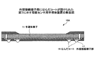
上述の指紋センサ用半導体装置10は、機器に組み込まれる前に、基板実装用の接合部材が外部接続端子12に設けられる。図5に示す例では、外部接続端子12にはんだボール18が設けられている。また、図6に示す例では、外部接続端子12にはんだがコーティングされてはんだコート19が形成されている。
The above-described
指紋センサ用半導体装置10を基板に実装する際は、はんだボール18やはんだコート19がはんだリフローにより溶融されてから固化することで、外部接続端子12が基板の端子に接合される。この際、外部接続端子12が封止樹脂13Bから突出した部分の側面にもはんだが固着するため、側面の面積だけ接合面積が増大したこととなり、実装信頼性が向上する。
When the fingerprint
次に、本発明の第2実施例による指紋センサ用半導体装置について、図7を参照しながら説明する。図7は本発明の第2実施例による指紋センサ用半導体装置の断面図である。図7において、図3に示す構成部品と同等な部品には同じ符号を付す。 Next, a semiconductor device for a fingerprint sensor according to a second embodiment of the present invention will be described with reference to FIG. FIG. 7 is a sectional view of a semiconductor device for a fingerprint sensor according to a second embodiment of the present invention. 7, parts that are the same as the parts shown in FIG. 3 are given the same reference numerals.
図7に示す指紋センサ用半導体装置10Aは、電極11aを有する半導体素子11と、電極11aの反対側で半導体素子11上に形成された外部接続端子部17と、外部接続端子部17側に設けられた封止樹脂13Bと、センサ面11b側に設けられた封止樹脂13Aとを有する。
A semiconductor device for
半導体素子11の電極11a及びセンサ面11bは、半導体素子11の回路形成面(以下、表面とも称する)に形成されるため、同じ面に設けられている。電極11aはセンサ面11bの周囲に配置される。
Since the
半導体素子11の背面(センサ面11bの反対側の面であり、裏面とも称する)には、配線(再配線とも称する)14が施され、配線14上に外部接続端子部17が形成されている。外部接続端子部17は、実質的に外部配線端子となる部分であるが、配線14と一体的に形成される場合もあるので、外部接続端子部と称する。
A wiring (also referred to as a rewiring) 14 is provided on the back surface of the semiconductor element 11 (the surface opposite to the
このように、半導体素子11の電極11aは半導体装置11の表面に形成され、外部接続端子部17は半導体素子11の裏面に設けられるため、電極11aと外部接続端子部17を電気的に接続する必要がある。本実施例では、半導体素子11の周囲部分において、半導体素子の表面から裏面へ貫通して延在する接続部15を設けて、電極11aと外部接続端子部17とを電気的に接続している。接続部15は、半導体素子11にスルーホールを形成して、その中に金属などの導電部材を充填することにより形成される。
Thus, since the
本実施例では、外部接続端子部17は、保護金属層が設けられた配線14の一部に相当する。半導体素子11の裏面側は、封止樹脂13Bにより覆われているが、外部接続端子部17の部分のみ封止樹脂13Bは設けられていない。すなわち、封止樹脂13Bに開口が設けられ、その中で外部接続端子部17が露出している。
In this embodiment, the external
一方、半導体素子11の表面側は、センサ面11bを残して、封止樹脂13Aにより覆われている。すなわち、センサ面11bの周囲に配置された電極11a及び接続部15の端部は封止樹脂13Aにより封止されている。
On the other hand, the surface side of the
なお、半導体素子11の裏面には絶縁層16が形成され、配線14は絶縁層16の上に形成されている。
Note that an insulating
本実施例では、半導体素子11を貫通した接続部15を設けて、表側の電極11aを裏側の配線14に電気的に接続することで、表側の電極11aと裏側の外部接続端子部17とを電気的に接続している。したがって、半導体素子11の外形より突出する部分が不要であり、指紋センサ用半導体装置10Aの外形は、半導体素子11の外形に等しくなる。これにより、指紋センサ用半導体装置10Aが占める面積(実装面積)が低減され、実質的にとり得る最小の面積となる。また、外部接続端子が配線14とは別個に形成されていないため、製造コストを低減することができる。更に、配線14をスパッタ金属膜のみで形成することで、更なる低コスト化が可能となる。
In the present embodiment, the
次に、半導体素子11の電極11aと外部接続端子部17とを電気的に接続する構造を形成する工程について説明する。図8は電極11aと外部接続端子部17とを電気的に接続する構造を形成する工程を示す図である。なお、図8に示す半導体素子11の一部は、図7に示す半導体素子11とは上下が反対となっている。また、以下に説明する工程は、半導体装置の製造工程で一般的に行われている技術を用いて行なうことができ、ここでは工程の概要のみを説明する。
Next, a process of forming a structure for electrically connecting the
ここで、図8(A)〜図8(C)に示す工程は、上述の図4(A)〜図4(C)に示す工程と同じであり、説明を省略する。 Here, the steps shown in FIGS. 8A to 8C are the same as the steps shown in FIGS. 4A to 4C, and the description thereof is omitted.
図8(C)に示す工程が終了する、次に、図8(D)に示すように、配線用レジスト23を除去して、配線14を露出させる。配線14は外部接続端子部17に相当する部分を含んでいる。
The process shown in FIG. 8C is completed. Next, as shown in FIG. 8D, the wiring resist 23 is removed and the
続いて、図8(E)に示すように、配線14を外部接続端子部用レジスト25で覆い、
外部接続端子部17に相当する部分だけ外部接続端子部用レジスト25を除去して開口を形成してから、開口内で露出した配線14の上に保護金属層17aを形成する。保護金属層17aは例えば、ニッケル(Ni)めっきと金(Au)めっきの2層構造である。
Subsequently, as shown in FIG. 8E, the
The external connection terminal portion resist 25 is removed only in a portion corresponding to the external
次に、外部接続端子部用レジスト25を全て除去してから、露出した配線下地金属層22及びその下の密着金属層21をエッチングにより除去する。配線14の上に保護金属層17aが設けられた部分が外部接続端子部17となる。ただし、保護金属層17aが不要な場合は、図8(E)に示す工程は省略され、封止樹脂13Bから露出された配線14の一部が外部接続端子部17となる。
Next, after all the external connection terminal portion resist 25 is removed, the exposed wiring base metal layer 22 and the adhesive metal layer 21 thereunder are removed by etching. A portion where the
以上の処理で、半導体素子11の表側の電極11aと裏側に形成された外部接続端子部17とが接続部15により電気的に接続された構造が形成される。
With the above processing, a structure in which the
以上の工程で外部接続端子部17を形成することにより、インターポーザを使用せずに指紋センサ用半導体装置10Aを形成することができ、半導体素子11と同じサイズの指紋センサ用半導体装置10Aを形成することができる。したがって、指紋センサ用半導体装置10Aの実装面積を縮小化することができる。
By forming the external
上述の指紋センサ用半導体装置10Aは、機器に組み込まれる前に、基板実装用の接合部材が外部接続端子部17に設けられる。図9に示す例では、外部接続端子部17にはんだボール18が設けられている。また、図10に示す例では、外部接続端子部17にはんだがコーティングされてはんだコート19が形成されている。
The above-described fingerprint
指紋センサ用半導体装置10を基板に実装する際は、はんだボール18やはんだコート19がはんだリフローにより溶融されてから固化することで、外部接続端子12が基板の端子に接合される。
When the fingerprint
さらに、図11に示す例では外部接続端子部17に突状端子20が設けられている。突状端子20は、例えばワイヤボンディングで形成されるスタッドバンプ等である。突状端子20は、例えば導電性接着剤等で基板の端子に接続される。
Furthermore, in the example shown in FIG. 11, the protruding terminal 20 is provided in the external
上述の実施例による指紋センサ用半導体装置10,10Aは、一枚のシリコンウェハに複数個まとめて形成した後で、各々を個片化することで効率的に製造することができる。以下に、指紋センサ用半導体装置(以下簡略化して半導体装置と称する)をウェハ状態でまとめて製造する際の利点について説明する。なお、以下の説明では、図3に示す指紋センサ用半導体装置10の製造を例にとって説明する。
The fingerprint
図12は側面も封止樹脂で覆われた半導体装置10の断面図である。図12に示す半導体装置10は、半導体素子11の側面(外周面)に表面側からと裏面側から続く傾斜面が形成され、表面側から続く傾斜面11cは上側の封止樹脂13Aにより覆われ、裏面から続く傾斜面11dは下側の封止樹脂13Bにより覆われている。
FIG. 12 is a cross-sectional view of the
このように、側面まで樹脂封止することにより、樹脂封止13A,13Bと半導体素子11との境目が、外部からの衝撃等のストレスから保護され、半導体素子11のカケや割れが防止される。また、封止樹脂13A,13Bと半導体素子11との密着面積が増加するので、樹脂密着強度が向上し、半導体装置10の信頼性が向上する。
Thus, by sealing the resin to the side surface, the boundary between the resin sealing 13A, 13B and the
なお、図12に示す例では、半導体素子11の表面側と裏面側の両方から続く傾斜面11c、11dが設けられているが、必ずしも両側に傾斜面を設ける必要はなく、いずれか一方側からの傾斜面だけであってもよい。
In the example shown in FIG. 12, the inclined surfaces 11 c and 11 d continuing from both the front surface side and the back surface side of the
ここで、上述の傾斜面11cの形成方法について、図13を参照しながら説明する。半導体装置10はウェハ(基板)状態で複数個を一括して製造するものとする。ウェハ状態で半導体装置10を製造する場合、ウェハをダイシングにより切断することにより、ウェハ上で繋がった各半導体装置10を個片化する。この際に、半導体素子11を樹脂封止する前に、図13(A)〜図13(C)に示すように、切断するために用いるダイシングブレードよりも幅の広いダイシングブレード26を使用して、ハーフカットを施す。ダイシングブレード26の先端をV字状としておくことで、半導体素子11に傾斜面11cが形成される。図13の例では、ダイシングラインの両側に半導体素子11が形成されおり、V字状のダイシングブレード26によりV溝を形成することで、両側の半導体素子11に同時に傾斜面11cが形成される。
Here, the formation method of the above-mentioned inclined surface 11c is demonstrated, referring FIG. A plurality of
傾斜面11cが形成された後、図13(D)に示すように、ウェハ全体を一括して樹脂封止し、封止樹脂13Aを半導体素子11上に設ける。この際、ハーフカットで形成されたV溝にも封止樹脂が充填される。
After the inclined surface 11c is formed, as shown in FIG. 13D, the entire wafer is sealed with resin, and a sealing
樹脂封止した後、図13(E)〜図13(G)に示すようにハーフカット用のダイシングブレード26より幅の小さなダイシングブレード27を用いてダイシングラインに沿ってウェハを切断することで、傾斜面11cが封止樹脂13Aで覆われた半導体装置10が個片化される。言い換えれば、ダイシングで削り取られる幅より大きな幅を有する溝をハーフカットにより形成して、半導体素子11の側面にも封止樹脂が形成されるようにしている。
After resin sealing, the wafer is cut along a dicing line using a
以上のように、ウェハ状態において、V溝を形成することで、半導体素子11に容易に傾斜面を形成することができ、側面の一部が封止樹脂で覆われた半導体装置10を容易に形成することができる。
As described above, by forming the V-groove in the wafer state, the inclined surface can be easily formed in the
なお、ハーフカット用のダイシングブレード26の形状を変更してV溝の形状を変更することで、半導体素子の側面の封止形状を変更することができる。
Note that the sealing shape of the side surface of the semiconductor element can be changed by changing the shape of the V-groove by changing the shape of the half-
次に、半導体素子の表側と裏側で異なる種類の封止樹脂を用いる場合について、図14及び図15を参照しながら説明する。 Next, the case where different types of sealing resin are used on the front side and the back side of the semiconductor element will be described with reference to FIGS. 14 and 15.
図14は図3に示す半導体装置10において、表側(センサ面側)の封止樹脂13Aと裏側(実装面側)の封止樹脂13Bとを異なる種類(異なる特性)の樹脂で形成した例を示す断面図である。
14 shows an example in which the front side (sensor surface side) sealing
図14に示す例では、センサ面、実装面ともに圧縮成型により封止樹脂成13A,13Bを成形する。この場合、樹脂の種類としては例えばモールド可能なエポキシ樹脂が選定されるが、実装面側に用いる封止樹脂13Bとして、
センサ面側に用いる封止樹脂13Aよりも線膨張係数αの大きな樹脂を選定する。したがって、センサ面側に対してはセンサ面とマッチングの良い樹脂(αが小さい)を選定することで環境ストレスなどによる樹脂ハガレ等を防止し、実装面側に対しては実装基板に近い(αが大きい)樹脂の選定することで実装環境ストレス耐性を向上させることができる。
In the example shown in FIG. 14, the sealing
A resin having a larger linear expansion coefficient α than the sealing
図15は図7に示す半導体装置10Aにおいて、表側(センサ面側)の封止樹脂13Aと裏側(実装面側)の封止樹脂13Bとを異なる種類(異なる特性)の樹脂で形成した例を示す断面図である。
FIG. 15 shows an example in which the front side (sensor surface side) sealing
図15に示す例では、センサ面側に圧縮成型により封止樹脂13Aを成形し、実装面側には印刷やスピンコートにより液状の樹脂を塗布して封止樹脂成13Bを成形している。実装面側の封止樹脂13Bとして、感光性の樹脂、例えばポリイミドやエポキシレジスト等を用いれば、外部接続端子部を露出させるための開口部を感光性樹脂のパターニング処理により形成することができる。
In the example shown in FIG. 15, the sealing
また、ウェハ状態での処理において、ウェハに反りが生じるような場合、ウェハの表面側及び裏面側に異なる特性の樹脂を選択することで、反りを防止することも可能である。 Further, when the wafer is warped during processing in the wafer state, it is possible to prevent the warpage by selecting resins having different characteristics on the front surface side and the back surface side of the wafer.
次に、上述の半導体装置10をウェハ(基板)状態で一括して製造する工程について、図16を参照しながら説明する。
Next, a process for manufacturing the above-described
まず、半導体製造用基板であるウェハ上で半導体素子11を一括して形成する。次に、図16(A)に示すように、導電部となる接続部15を各半導体素子11に形成する(電極裏面移設工程)。そして、図16(B)に示すように、配線14を施してその上に外部接続端子12を形成する(再配置配線工程)。
First, the
続いて、図16(C)に示すように、ウェハの表面側及び裏面側に封止樹脂13A及び封止樹脂13Bを形成する(樹脂封止工程)。そして、図16(D)に示すように、外部接続端子12の先端にはんだボール18を設ける(端子形成工程)。
Subsequently, as shown in FIG. 16C, a sealing
その後、図16(E)に示すように、ウェハ状態のまま各半導体装置10にコンタクタ28を接触させて各半導体装置10の電気的特性試験を行なう。
Thereafter, as shown in FIG. 16E, the
次に、図16(F)に示すように、ウェハの表面側にダイシングテープ29を貼り付けてウェハを上下逆にし、ダイシングにより切断して半導体装置10を個片化する(個片分割工程)。個片化した半導体装置10をダイシングテープ29から剥がすことにより、図16(G)に示すように、複数の半導体装置10を一括して製造することができる。
Next, as shown in FIG. 16F, a dicing
以上の工程により、ウェハサイズを統一して汎用性のある装置を使用することができ、開発費や設備投資費の低減、及び製造対応期間の短縮が可能となる。また、組立やテスト処理能力を向上させることが出来るので、コストの低減化を行うことができる。 Through the above steps, a versatile apparatus can be used with a uniform wafer size, and it is possible to reduce development costs and capital investment costs and shorten the manufacturing response period. In addition, since the assembly and test processing capability can be improved, the cost can be reduced.
次に、半導体素子11を樹脂封止する方法の一例について、図17乃至図22を参照しながら説明する。
Next, an example of a method for resin-sealing the
まず、図17(A)に示すように、半導体素子11が形成されたウェハを圧縮成形用の金型(上型30及び下型31A,31B)内に配置する。この際、外部接続端子12を上型30に向けた状態とし、ウェハと上型30との間に弾性シート材32を配置する。樹脂材は弾性シート材32とウェハとの間に供給される。弾性シート材32は、樹脂と密着しない、例えば、フッ素系樹脂からなる弾性を持つシート材である。また、ウェハと下型31A,31Bとの間には、やはりフッ素樹脂系のシート材33が配置される。
First, as shown in FIG. 17A, the wafer on which the
金型を閉じて、下型31Bを上型30に向けて押圧することで、供給した樹脂を流動させ、圧縮成型を行なう。この際、下型31Bによりウェハは上型30に向けて押圧されるため、ウェハ上の外部接続端子12の先端は図18(A)に示す状態から図18(B)に示す状態となる。すなわち、外部接続端子12の先端は、弾性シート材32に食い込んだ状態となる。図18(B)に示す状態で、金型内で樹脂が流動し、圧縮成型により封止樹脂13Bが形成される。
By closing the mold and pressing the
圧縮成型が終了したら、図17(C)に示すように、金型を開いて裏面が樹脂封止されたウェハを金型から取り出す。図19は金型から取り出され状態のウェハを示す断面図である。弾性シート材32に食い込んだ部分の外部接続端子12が封止樹脂13Bから突出している。外部接続端子12の封止樹脂13Bからの突出量は、図18(B)に示すように、弾性シート材32への食い込み量Xに等しい。
When the compression molding is completed, as shown in FIG. 17C, the mold is opened, and the wafer whose back surface is sealed with resin is taken out from the mold. FIG. 19 is a cross-sectional view showing the wafer taken out from the mold. The portion of the
なお、弾性シート材32及びシート材33は封止樹脂と密着しないシートであり、これを介在させることで、通常、金型との型離れを行うために樹脂に添加されている離型剤を使用しないで成型することができるので、高密着な樹脂層(封止樹脂)を得ることができる。また、弾性シート材32を介在させることで、金型とセンサ面との接触を防ぎ、センサ面を保護することができる。
The elastic sheet material 32 and the
ウェハの裏側(実装面側)の樹脂封止が終了したら、次に、ウェハの表側(センサ面側)の樹脂封止を行なう。図20はウェハの表側の樹脂封止工程を示す図である。図20(A)は金型にウェハをセットした状態を示し、図20(B)は金型を閉じて樹脂を圧縮成型している状態を示し、図20(C)は圧縮成型が終了して金型を開いた状態を示す。 When the resin sealing on the back side (mounting surface side) of the wafer is completed, the resin sealing on the front side (sensor surface side) of the wafer is then performed. FIG. 20 is a view showing a resin sealing process on the front side of the wafer. 20A shows a state in which a wafer is set in a mold, FIG. 20B shows a state in which the mold is closed and resin is compression-molded, and FIG. 20C shows that compression molding has been completed. The mold is opened.
裏側の樹脂封止工程と同様に、圧縮成型により封止樹脂13Aが成型される。ただし、上型30には、各半導体素子11のセンサ面11bに対応する位置に突部30aが設けられている。ウェハが金型にセットされて下型31Bにより押圧された際、突部30aは各半導体素子11のセンサ面11bに当接する。これにより、センサ面11b上には封止樹脂が流れ込まなくなり、結果としてセンサ面11bが露出した状態で樹脂封止が行なわれる。なお、ウェハと上型30及び下型31A,31Bとの間には、シート材33が配置される。
Similar to the resin sealing process on the back side, the sealing
図21(A)は金型から取り出した状態のウェハの断面図である。このウェハを半導体素子11の境界部分、すなわち、ダイシングラインに沿って切断することにより、図21(B)に示すように複数の半導体装置10が個片化される。
FIG. 21A is a cross-sectional view of the wafer taken out from the mold. By cutting the wafer along the boundary portion of the
なお、上述の樹脂封止工程は、ウェハの裏側と表側の樹脂封止を異なる工程としたが、図22に示すように、ウェハの裏面を下型31Bに向けてセンサ面11bを上型に向けてウェハを配置し、ウェハと下型31A,31Bとの間に弾性シート材32を配置し、上型30に突部30aを設けることで、ウェハの表側と裏側を一つの金型で同時に樹脂封止することができる。
In the above-described resin sealing step, the resin sealing on the back side and the front side of the wafer is different, but as shown in FIG. 22, the back surface of the wafer faces the
また、ウェハの表側(センサ面側)の樹脂封止を、圧縮成型ではなく、印刷法により行なうこともできる。図23は印刷法により樹脂封止する工程を示す図である。 Also, resin sealing on the front side (sensor surface side) of the wafer can be performed by a printing method instead of compression molding. FIG. 23 is a diagram showing a step of resin sealing by a printing method.
まず、図17に示す圧縮成型工程により、ウェハの裏側(実装面側)の樹脂封止を行ない封止樹脂13Bを形成しておく。次に、図23(A)に示すように、封止樹脂13Aが設けられる部分が開口している印刷マスク34を準備する。そして、図23(B)に示すように、印刷マスク34をウェハの表面上においてペースト又は液状樹脂をスキージを用いて印刷マスク34の開口に充填し、硬化させる。
First, by the compression molding process shown in FIG. 17, the resin sealing of the back side (mounting surface side) of the wafer is performed to form the sealing
そして、図23(C)に示すように、印刷マスク34をウェハから取り外すと、センサ面11bが露出した状態で封止樹脂13Aがウェハ上に残る。その後、図23(D)に示すように、外部接続端子12にはんだボール18を設けてから、ウェハをダイシングすることにより、複数の半導体装置10を得ることができる。
Then, as shown in FIG. 23C, when the
また、ウェハの表側(センサ面側)の封止封止を光硬化型樹脂として、パターニングマスクを用いて樹脂封止することもできる。図24は、パターニングマスクを用いてウェハのセンサ面側を樹脂封止する工程を示す図である。 Further, the front side (sensor surface side) of the wafer can be sealed with a photo-curing resin and can be sealed with a patterning mask. FIG. 24 is a diagram illustrating a process of resin-sealing the sensor surface side of the wafer using a patterning mask.
まず、図17に示す圧縮成型工程により、ウェハの裏側(実装面側)の樹脂封止を行ない封止樹脂13Bを形成しておく。次に、図24(A)に示すように、ウェハと同じ大きさの開口を有するマスク35を準備する。そして、図24(B)に示すように、マスク35をウェハの表面上においてペースト又は液状の感光性樹脂をスキージを用いてマスク35の開口に充填し、図24(C)に示すようにウェハの表面全体に感光性樹脂を塗布する。
First, by the compression molding process shown in FIG. 17, the resin sealing of the back side (mounting surface side) of the wafer is performed to form the sealing
続いて、図24(D)に示すように、パターニングマスク36を介して感光性樹脂を露光させ、硬化させる。パターニングマスク36は、各半導体素子11のセンサ面11bを除く部分に光を照射できるようにパターン化されている。したがって、センサ面11bに相当する部分の感光性樹脂は硬化せず、センサ面11b以外の部分の感光性樹脂のみ硬化する。
Subsequently, as shown in FIG. 24D, the photosensitive resin is exposed and cured through the patterning mask 36. The patterning mask 36 is patterned so that light can be applied to the portions of the
したがって、図24(E)に示すように、硬化しなかった感光性樹脂を取り除くことによりセンサ面11bが露出し、且つ硬化した封止樹脂13Aがウェハ上に残る。その後、図24(F)に示すように、外部接続端子12にはんだボール18を設けてから、ウェハをダイシングすることにより、複数の半導体装置10を得ることができる。
Therefore, as shown in FIG. 24E, the
また、ウェハの裏面側(実装面側)を印刷法を用いて樹脂封止することもできる。図25は印刷法を用いてウェハの裏面を樹脂封止する工程を示す図である。 In addition, the back side (mounting side) of the wafer can be resin-sealed using a printing method. FIG. 25 is a diagram showing a step of resin-sealing the back surface of the wafer using a printing method.
まず、図20に示す圧縮成型工程により、ウェハの表側(センサ面側)の樹脂封止を行ない封止樹脂13Aを形成しておく。次に、図25(A)に示すように、封止樹脂13Bに対応するパターンの開口を有する印刷マスク37を準備する。そして、図25(B)に示すように、印刷マスク37をウェハの表面上においてペースト又は液状の樹脂をスキージを用いて印刷マスク37の開口に充填し、硬化させる。
First, by the compression molding step shown in FIG. 20, the front side (sensor surface side) of the wafer is sealed with resin to form a sealing
そして、図25(C)に示すように、印刷マスク37をウェハから取り外すと、外部接続端子部17が露出した状態で封止樹脂13Bがウェハ上に残る。その後、図25(D)に示すように、外部接続端子部17にはんだボール18を設けてから、ウェハをダイシングすることにより、複数の半導体装置10Aを得ることができる。
Then, as shown in FIG. 25C, when the
また、ウェハの裏側(実装面側)の封止樹脂を光硬化型樹脂として、パターニングマスクを用いて樹脂封止することもできる。図26は、パターニングマスクを用いてウェハの実装面側を樹脂封止する工程を示す図である。 Further, the sealing resin on the back side (mounting surface side) of the wafer can be used as a photo-curing resin, and can be sealed with a patterning mask. FIG. 26 is a diagram illustrating a process of resin-sealing the mounting surface side of the wafer using the patterning mask.
まず、図20に示す圧縮成型工程により、ウェハの裏側(実装面側)の樹脂封止を行ない封止樹脂13Bを形成しておく。次に、図25(A)に示すように、ウェハと同じ大きさの開口を有するマスク35を準備する。そして、図25(B)に示すように、マスク38をウェハの表面上においてペースト又は液状の感光性樹脂をスキージを用いてマスク38の開口に充填し、図25(C)に示すようにウェハの裏面全体に感光性樹脂を塗布する。
First, resin sealing on the back side (mounting surface side) of the wafer is performed by the compression molding process shown in FIG. 20 to form a sealing
続いて、図25(D)に示すように、パターニングマスク39を介して感光性樹脂を露光させ、硬化させる。パターニングマスク39は、各半導体素子11の封止樹脂13Bを設ける部分に光を照射できるようにパターン化されている。したがって、外部接続端子部17が露出する部分に相当する感光性樹脂は硬化せず、これ以外の部分の感光性樹脂のみ硬化する。
Subsequently, as shown in FIG. 25D, the photosensitive resin is exposed and cured through the
したがって、図25(E)に示すように、硬化しなかった感光性樹脂を取り除くことにより外部接続端子部17が内部に露出した開口を有する封止樹脂13Bがウェハ上に残る。その後、図25(F)に示すように、外部接続端子部17にはんだボール18を設けてから、ウェハをダイシングすることにより、複数の半導体装置10Aを得ることができる。
Therefore, as shown in FIG. 25E, the sealing
また、ウェハの裏面側(実装面側)をスピンコート法を用いて樹脂封止することもできる。図27はスピンコート法を用いてウェハの裏面を樹脂封止する工程を示す図である。 Further, the back surface side (mounting surface side) of the wafer can be resin-sealed by using a spin coating method. FIG. 27 is a diagram showing a step of resin-sealing the back surface of the wafer using a spin coating method.
まず、図20に示す圧縮成型工程により、ウェハの裏側(実装面側)の樹脂封止を行ない封止樹脂13Bを形成しておく。次に、図27(A)に示すように、液状の感光性樹脂をウェハの実装面上に滴下しながらウェハを回転し、図27(B)に示すように、感光性樹脂をウェハの裏面全体に一様な厚みで行き渡らせる。
First, resin sealing on the back side (mounting surface side) of the wafer is performed by the compression molding process shown in FIG. 20 to form a sealing
続いて、図27(C)に示すように、パターニングマスク39を介して感光性樹脂を露光させ、硬化させる。パターニングマスク39は、各半導体素子11の封止樹脂13Bを設ける部分に光を照射できるようにパターン化されている。したがって、外部接続端子部17が露出する部分に相当する感光性樹脂は硬化せず、これ以外の部分の感光性樹脂のみ硬化する。
Subsequently, as shown in FIG. 27C, the photosensitive resin is exposed and cured through the
したがって、図27(D)に示すように、硬化しなかった感光性樹脂を取り除くことにより外部接続端子部17が内部に露出した開口を有する封止樹脂13Bがウェハ上に残る。その後、図25(E)に示すように、外部接続端子部17にはんだボール18を設けてから、ウェハをダイシングすることにより、複数の半導体装置10Aを得ることができる。
Therefore, as shown in FIG. 27D, the sealing
ここで、図20に示す圧縮成型において、シート材31を介して凸部30aをセンサ面11bに押し付けることでセンサ面11b上に封止樹脂が流れ込まないようにしているが、押圧の程度や、成型条件等のばらつきにより、シート材31とセンサ面11bとの間に僅かに樹脂が侵入し、その結果、図28(A)に示すように、樹脂バリ(樹脂の薄い膜)13Aaがセンサ面11bに形成されるおそれがある。
Here, in the compression molding shown in FIG. 20, the sealing resin is prevented from flowing onto the
そこで、樹脂バリ13Aaを除去するために、封止樹脂13Aを圧縮成型した後で、図28(B)に示すように、ウェハのセンサ面側にプラズマを照射してアッシング処理を行なう。アッシング処理により樹脂バリ13Aaは疎化されて脆弱となり、センサ面11bへの密着力も弱まるため、簡単に除去することができる。
Therefore, in order to remove the resin burr 13Aa, after the sealing
すなわち、図28(C)に示すように、アッシング処理した樹脂バリ13Aaをスクラブ処理(ウェハを回転させながらブラッシングと水洗処理を行なう)により除去し、図28(D)に示すように、センサ面11bを確実に露出させる。 That is, as shown in FIG. 28C, the ashed resin burr 13Aa is removed by scrubbing (brushing and rinsing while rotating the wafer), and as shown in FIG. 11b is exposed reliably.
なお、実装面側で外部接続端子12や外部接続17の上にも樹脂バリが形成されるおそれがある場合、これらの部分にも上述のアッシング処理を行なって樹脂バリを除去することができる。また、図28には一つの半導体装置の樹脂バリを除去する工程が示されているが、樹脂バリの除去はウェハ状態で行なうことが好ましい。
If there is a possibility that resin burrs are also formed on the
次に、上述のようにウェハをダイシングにより切断する際に位置検出に用いる認識マークについて説明する。 Next, a recognition mark used for position detection when the wafer is cut by dicing as described above will be described.
図29はセンサ面に認識マークが設けられた半導体装置10の断面図であり、図30は図29におけるセンサ面を上から見た平面図である。上述の実施例による指紋センサ用半導体装置10において、封止樹脂13Aから露出したセンサ面11bの中に、認識マーク(インデックスマーク)40が設けられる。認識マーク40は、半導体素子11の回路形成面で配線を形成する工程にいおいて、ダミーパターンとして形成される。配線が例えばアルミ配線である場合、認識マーク40もアルミで形成される。
FIG. 29 is a cross-sectional view of the
認識マーク40は、封止樹脂13Aから露出したセンサ面11bに設けられているので、最終工程においてダイシングによりウェハを切断する際、センサ面11bを上面にしてウェハをセットして切断することで、切断位置の位置決めに用いることができる。すなわち、センサ面11bに設けられた認識マーク40を認識しながら半導体素子11の境界部分(すなわち、ダイシングライン)の位置を決定し、ダイシングを行なうことができる。
Since the
以上のように、センサ面に認識マーク40を設けることで、通常行なわれているようにダイシング時の認識マークとして使用されているセンサ面の外形位置を認識させた場合よりも、高精度でダイシングすることが可能となる。センサ面の外形は封止樹脂により画成されており、また、ウェハと金型の位置合わせにより精度が決まっており、ウェハ自体の位置と誤差が生じる場合があるためである。
As described above, by providing the
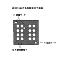
図31は実装面に認識マークが設けられた半導体装置10の断面図であり、図32は図31における実装面を下から見た平面図である。上述の実施例による指紋センサ用半導体装置10において、実装面側に再配線技術により認識用マーク41が設けられている。認識マーク41の形成は、外部接続端子12や外部端子部17と同様に、再配線技術を用いて形成される。認識マーク41も、外部接続端子12や外部接続端子部17と同様に、封止樹脂13Bから露出させられている。
FIG. 31 is a cross-sectional view of the
認識マーク41は、封止樹脂13Bから露出して設けられているので、最終工程においてダイシングによりウェハを切断する際、実装面を上面にしてウェハをセットして切断することで、切断位置の位置決めに用いることができる。すなわち、実装面に露出した認識マーク41を認識しながらダイシングラインの位置を決定し、ダイシングを行なうことができる。
Since the
以上のように、実装面に認識マーク41を設けることで、通常行なわれているように外部接続用端子に設けられたはんだボール等を認識させる場合よりも、高精度でダイシングすることが可能となる。はんだボールは、はんだを溶融して接合している。はんだボールのサイズバラツキやはんだボールの形状バラツキ、はんだボールの搭載精度の影響が切断位置に誤差を生じさせる場合があるためである。
As described above, by providing the
ここで、上述の図29及び図30に示す認識マーク40は、半導体装置を個片化する際に用いられるだけでなく、図13に示す傾斜面を形成するためのV溝を形成する工程においても位置認識用として用いることができる。図32はV溝形成工程とダイシング工程の両方で、同じ認識マークを用いることを説明するための図である。
Here, the
まず、図33(A)に示すように、ウェハ上において各センサ面11bに設けられた認識マーク40を画像認識してV溝を入れる位置(すなわち、半導体素子の境界部分であるダイシングライン)を決定し、図33(B)に示すように、V字状のダイシングブレードによりハーフカットを施してV溝を形成する(ハーフカットは図13を参照)。
First, as shown in FIG. 33 (A), a position where a
次に、封止樹脂13Aを形成した後、個片化工程において、図33(C)に示すように、各センサ面11bに設けられた認識マーク40を再度画像認識してウェハ上でダイシングラインを決定し、図33(D)に示すようにダイシングして半導体装置10を個片化する。
Next, after forming the sealing
以上の方法によれば、ハーフカット時とダイシング時のダイシングラインの認識を、同じ認識マーク40を用いて行なうため、ハーフカットの位置(V溝の位置)とダイシングの位置とが精度よく一致する。このため、図12に示す半導体素子11の傾斜面11cを精度良く形成することができ、半導体素子11の側部も確実に樹脂封止することができる。
According to the above method, since the
上述のハーフカット時とダイシング時のダイシングラインの認識を同じ認識マークを用いる方法は、ウェハの実装面側に認識マーク41を形成した場合にも用いることができる。すなわち、ウェハ上において配線14上に設けられた認識マーク41を画像認識してV溝を入れる位置(すなわち、半導体素子の境界部分であるダイシングライン)を決定し、V字状のダイシングブレードによりハーフカットを施してV溝を形成する(ハーフカットは図13を参照)。そして、封止樹脂13Bを形成した後、個片化工程において、封止樹脂13Bから露出した認識マーク41を再度画像認識してウェハ上でダイシングラインを決定し、ダイシングして半導体装置10を個片化する。
The method of using the same recognition mark for the recognition of the dicing line at the time of half-cutting and dicing can also be used when the
以上説明したように、本明細書は以下の発明を開示する。 As described above, the present specification discloses the following invention.
(付記1)
所定の機能を提供する機能面を有する半導体装置であって、
電極が形成された回路形成面と該回路形成面の反対側の背面とを有し、該回路形成面の一部が前記機能面として機能する半導体素子と、
該半導体素子の前記背面上に形成された配線と、
前記半導体素子の前記回路形成面と前記背面との間を貫通して延在し、前記電極と該配線とを電気的に接続する接続部と、
前記配線に接続され、前記半導体素子の前記背面側で前記半導体装置の外部に露出した外部接続端子と
を有することを特徴とする半導体装置。
(Appendix 1)
A semiconductor device having a functional surface that provides a predetermined function,
A semiconductor element having a circuit forming surface on which an electrode is formed and a back surface opposite to the circuit forming surface, wherein a part of the circuit forming surface functions as the functional surface;
Wiring formed on the back surface of the semiconductor element;
A connection portion extending between the circuit forming surface and the back surface of the semiconductor element and electrically connecting the electrode and the wiring;
An external connection terminal connected to the wiring and exposed to the outside of the semiconductor device on the back side of the semiconductor element.
(付記2)
付記1記載の半導体装置であって、
前記配線は封止樹脂により封止され、前記外部接続端子は該封止樹脂の表面から突出していることを特徴とする半導体装置。
(Appendix 2)
A semiconductor device according to
The semiconductor device, wherein the wiring is sealed with a sealing resin, and the external connection terminal protrudes from the surface of the sealing resin.
(付記3)
付記2記載の半導体装置であって、
前記外部接続端子に、はんだボール、はんだコート、のうちいずれか一つが設けられていることを特徴とする半導体装置。
(Appendix 3)
The semiconductor device according to
Any one of a solder ball and a solder coat is provided on the external connection terminal.
(付記4)
付記1記載の半導体装置であって、
前記配線は封止樹脂により封止され、前記外部接続端子は該封止樹脂に設けられた開口内で露出していることを特徴とする半導体装置。
(Appendix 4)
A semiconductor device according to
2. The semiconductor device according to
(付記5)
付記4記載の半導体装置であって、
前記外部接続端子に、はんだボール、はんだコート、前記外部接続端子よりも小さい面積の突状端子、のうちいずれか一つが設けられていることを特徴とする半導体装置。
(Appendix 5)
A semiconductor device according to appendix 4, wherein
A semiconductor device, wherein the external connection terminal is provided with any one of a solder ball, a solder coat, and a protruding terminal having a smaller area than the external connection terminal.
(付記6)
付記1記載の半導体装置であって、
前記半導体素子の前記回路形成面は、前記機能面が露出するように封止樹脂により封止され、該封止樹脂は前記半導体素子の側面の少なくとも一部を覆っていることを特徴とする半導体装置。
(Appendix 6)
A semiconductor device according to
The circuit forming surface of the semiconductor element is sealed with a sealing resin so that the functional surface is exposed, and the sealing resin covers at least a part of the side surface of the semiconductor element. apparatus.
(付記7)
付記6記載の半導体装置であって、
前記半導体素子の側面は前記回路形成面に垂直な面から傾斜した傾斜面を含み、該傾斜面が前記封止樹脂により覆われていることを特徴とする半導体装置。
(Appendix 7)
The semiconductor device according to appendix 6, wherein
A side surface of the semiconductor element includes an inclined surface inclined from a plane perpendicular to the circuit forming surface, and the inclined surface is covered with the sealing resin.
(付記8)
付記1記載の半導体装置であって、
前記半導体素子の前記背面に形成された前記配線は、前記外部接続用端子が露出するように封止樹脂により封止され、該封止樹脂は前記半導体素子の側面の少なくとも一部を覆っていることを特徴とする半導体装置。
(Appendix 8)
A semiconductor device according to
The wiring formed on the back surface of the semiconductor element is sealed with a sealing resin so that the external connection terminals are exposed, and the sealing resin covers at least a part of the side surface of the semiconductor element. A semiconductor device.
(付記9)
付記8記載の半導体装置であって、
前記半導体素子の側面は前記背面に垂直な面から傾斜した傾斜面を含み、該傾斜面が前記封止樹脂により覆われていることを特徴とする半導体装置。
(Appendix 9)
The semiconductor device according to
The semiconductor device is characterized in that a side surface of the semiconductor element includes an inclined surface inclined from a surface perpendicular to the back surface, and the inclined surface is covered with the sealing resin.
(付記10)
付記1記載の半導体装置であって、
前記半導体素子の前記回路形成面は、前記機能面が露出するように第1の封止樹脂により封止され、
前記半導体素子の前記背面に形成された前記配線は、前記外部接続端子が露出するように第2の封止樹脂により封止され、
前記第1の封止樹脂と前記第2の封止樹脂は、特性が異なる樹脂であることを特徴とする半導体装置。
(Appendix 10)
A semiconductor device according to
The circuit forming surface of the semiconductor element is sealed with a first sealing resin so that the functional surface is exposed,
The wiring formed on the back surface of the semiconductor element is sealed with a second sealing resin so that the external connection terminal is exposed,
The semiconductor device according to
(付記11)
付記1乃至10記載の半導体装置であって、
前記機能面に、前記半導体素子の回路形成面に形成された配線と同じ材料で形成された認識マークが設けられていることを特徴とする半導体装置。
(Appendix 11)
The semiconductor device according to
A semiconductor device, wherein a recognition mark made of the same material as a wiring formed on a circuit formation surface of the semiconductor element is provided on the functional surface.
(付記12)
付記1乃至11のうちいずれか一項記載の半導体装置であって、
前記半導体素子の前記機能面は、指紋検出用のセンサ面であることを特徴とする半導体装置。
(Appendix 12)
The semiconductor device according to any one of
The semiconductor device according to
(付記13)
電極が形成された回路形成面と該回路形成面の反対側の背面とを有し、該回路形成面の一部が所定の機能を提供する機能面として機能する半導体素子を有する、複数の半導体装置の製造方法であって
基板に整列して形成された複数の前記半導体素子の各々において、電極に電気的に接続され、前記半導体素子の前記回路形成面と前記背面との間を貫通して延在する接続部を導電部材により形成し、
前記半導体素子の各々において、該接続部に接続された配線を前記背面上に形成し、
前記半導体素子の各々において、該配線に接続された外部接続端子を形成し、
前記半導体素子を前記基板に形成された状態で、前記機能面及び前記外部接続端子が露出するように一括して樹脂封止し、
複数の前記半導体装置が基板中で形成された状態で、前記半導体装置の各々に電気的試験を施し、
前記基板を前記半導体素子の境界部分で切断して個片化することにより複数の前記半導体装置を一括して形成する
ことを特徴とする半導体装置の製造方法。
(Appendix 13)
A plurality of semiconductors having a circuit forming surface on which an electrode is formed and a back surface opposite to the circuit forming surface, and a semiconductor element in which a part of the circuit forming surface functions as a functional surface providing a predetermined function A method of manufacturing an apparatus, wherein each of the plurality of semiconductor elements formed in alignment with a substrate is electrically connected to an electrode and penetrates between the circuit formation surface and the back surface of the semiconductor element. The extending connection part is formed of a conductive member,
In each of the semiconductor elements, a wiring connected to the connection portion is formed on the back surface,
In each of the semiconductor elements, an external connection terminal connected to the wiring is formed,
In a state where the semiconductor element is formed on the substrate, the resin is collectively sealed so that the functional surface and the external connection terminal are exposed,
In a state where a plurality of the semiconductor devices are formed in a substrate, each of the semiconductor devices is subjected to an electrical test,
A method of manufacturing a semiconductor device, wherein the plurality of semiconductor devices are collectively formed by cutting the substrate at a boundary portion of the semiconductor element into pieces.
(付記14)
付記13記載の半導体装置の製造方法であって、
前記樹脂封止は金型を用いた樹脂の圧縮成型法により行ない、該金型は前記機能面に対応する位置に突出部を有しており、該金型と前記基板との間に該樹脂に対して密着しないシート在を介在させることを特徴とする半導体装置の製造方法。
(Appendix 14)
A method for manufacturing a semiconductor device according to
The resin sealing is performed by a resin compression molding method using a mold, and the mold has a protruding portion at a position corresponding to the functional surface, and the resin is interposed between the mold and the substrate. A method for manufacturing a semiconductor device, comprising interposing a sheet that is not in close contact with the substrate.
(付記15)
付記13記載の半導体装置の製造方法であって、
前記樹脂封止の工程は、
前記基板に形成された複数の前記半導体素子の前記回路形成面上に、前記機能面以外の部分に相当する部分に開口を有する印刷マスクを配置し、
該印刷マスクを介して液状の樹脂を前記回路形成面に塗布し、
該液状の樹脂を硬化させてから前記前記印刷マスクを取り外す
ことを含むことを特徴とする半導体装置の製造方法。
(Appendix 15)
A method for manufacturing a semiconductor device according to
The resin sealing step includes
A print mask having an opening in a portion corresponding to a portion other than the functional surface is disposed on the circuit formation surface of the plurality of semiconductor elements formed on the substrate,
Applying a liquid resin to the circuit forming surface through the printing mask,
A method of manufacturing a semiconductor device, comprising: removing the print mask after curing the liquid resin.
(付記16)
付記13記載の半導体装置の製造方法であって、
前記樹脂封止の工程の後に、前記機能面及び外部接続端子の少なくとも一方に対してアッシング処理を行ない、前記樹脂封止による樹脂バリを除去することを特徴とする半導体装置の製造方法。
(Appendix 16)
A method for manufacturing a semiconductor device according to
After the resin sealing step, at least one of the functional surface and the external connection terminal is subjected to an ashing process to remove resin burrs due to the resin sealing.
(付記17)
付記13記載の半導体装置の製造方法であって、
前記半導体素子の前記回路形成面に配線を形成する際に、前記機能面に該配線と同時に認識マークを形成し、
該認識マークを用いて前記境界部分を認識しながら、前記基板を切断して前記半導体装置を個片化することを特徴とする半導体装置の製造方法。
(Appendix 17)
A method for manufacturing a semiconductor device according to
When forming a wiring on the circuit forming surface of the semiconductor element, a recognition mark is formed simultaneously with the wiring on the functional surface,
A method of manufacturing a semiconductor device, wherein the semiconductor device is separated into pieces by cutting the substrate while recognizing the boundary portion using the recognition mark.
(付記18)
付記17記載の半導体装置の製造方法であって、
前記基板を切断して前記半導体装置を個片化する前に、前記認識マークを用いて前記境界部分を認識しながら、前記切断で削り取られる部分の幅より大きい幅の溝を前記境界部分に沿って形成することを特徴とする半導体装置の製造方法。
(Appendix 18)
A method for manufacturing a semiconductor device according to
Before cutting the substrate and dividing the semiconductor device into individual pieces, while recognizing the boundary portion using the recognition mark, a groove having a width larger than the width of the portion scraped off by the cutting is formed along the boundary portion. A method for manufacturing a semiconductor device, characterized by comprising:
(付記19)
付記13記載の半導体装置の製造方法であって、
前記半導体素子の前記背面に前記外部接続端子を形成する際に、前記外部接続端子と同時に認識マークを形成し、
該認識マークを用いて前記境界部分を認識しながら、前記基板を切断して前記半導体装置を個片化することを特徴とする半導体装置の製造方法。
(Appendix 19)
A method for manufacturing a semiconductor device according to
When forming the external connection terminal on the back surface of the semiconductor element, forming a recognition mark simultaneously with the external connection terminal,
A method of manufacturing a semiconductor device, wherein the semiconductor device is separated into pieces by cutting the substrate while recognizing the boundary portion using the recognition mark.
(付記20)
付記19記載の半導体装置の製造方法であって、
前記基板を切断して前記半導体装置を個片化する前に、前記認識マークを用いて前記境界部分を認識しながら、前記切断で削り取られる部分の幅より大きい幅の溝を前記境界部分に沿って形成することを特徴とする半導体装置の製造方法。
(Appendix 20)
A method for manufacturing a semiconductor device according to appendix 19, wherein
Before cutting the substrate and dividing the semiconductor device into individual pieces, while recognizing the boundary portion using the recognition mark, a groove having a width larger than the width of the portion scraped off by the cutting is formed along the boundary portion. A method for manufacturing a semiconductor device, characterized by comprising:
10,10A 指紋センサ用半導体装置
11 半導体素子
11a 電極
11b センサ面
11c,11d 傾斜面
12 外部接続端子
12a 保護金属層
13A,13B 封止樹脂
14 配線
15 接続部
16 絶縁層
17 外部接続端子部
17a 保護金属層
18 はんだボール
19 はんだコート
20 突状端子
23 配線レジスト
24 外部接続端子用レジスト
26,27 ダイシングブレード
30 上型
31A,31B 下型
32 弾性シート材
33 シート材
34,37 印刷マスク
35,38 マスク
36,39 パターニングマスク
40,41 認識マーク
DESCRIPTION OF
Claims (1)
電極が形成された回路形成面と該回路形成面の反対側の背面とを有し、該回路形成面の一部が前記機能面として機能する半導体素子と、
前記回路形成面に設けられた電極と、
前記回路形成面の前記機能面以外を覆う絶縁層と、
該絶縁層上に形成され、前記回路形成面の前記電極に接続された第1の配線と、
前記絶縁層と前記第1の配線とを覆う第1の封止樹脂と、
前記半導体素子の前記背面上に形成された第2の配線と、
前記第2の配線を覆う第2の封止樹脂と、
前記半導体素子の前記回路形成面と前記背面との間を貫通して延在し、前記第1の配線と前記第2の配線とを電気的に接続する接続部と、
前記第2の配線に接続され、該第2の封止樹脂の表面から突出し、前記半導体素子の前記背面側で前記半導体装置の外部に露出した外部接続端子と
を有し、
前記半導体素子の側面は、前記第1の封止樹脂に覆われた前記回路形成面側の第1の傾斜面と、前記第2の封止樹脂に覆われた前記背面側の第2の傾斜面と、前記第1及び第2の傾斜面の間に位置し前記第1及び第2の封止樹脂のいずれにも覆われない露出面とを有することを特徴とする半導体装置。 A semiconductor device having a functional surface that provides a predetermined function,
A semiconductor element having a circuit forming surface on which an electrode is formed and a back surface opposite to the circuit forming surface, wherein a part of the circuit forming surface functions as the functional surface;
Electrodes provided on the circuit forming surface;
An insulating layer covering the circuit forming surface other than the functional surface;
A first wiring formed on the insulating layer and connected to the electrode on the circuit formation surface;
A first sealing resin covering the insulating layer and the first wiring;
A second wiring formed on the back surface of the semiconductor element;
A second sealing resin covering the second wiring;
A connection portion extending between the circuit formation surface and the back surface of the semiconductor element and electrically connecting the first wiring and the second wiring;
Connected to said second wiring protrudes from the surface of the sealing resin of the second, have a external connection terminals exposed to the outside of the semiconductor device in the back side of the semiconductor element,
The side surface of the semiconductor element includes a first inclined surface on the circuit forming surface side covered with the first sealing resin, and a second inclined surface on the back side covered with the second sealing resin. And a exposed surface that is located between the first and second inclined surfaces and is not covered with any of the first and second sealing resins .
Priority Applications (3)
| Application Number | Priority Date | Filing Date | Title |
|---|---|---|---|
| JP2005093001A JP4731191B2 (en) | 2005-03-28 | 2005-03-28 | Semiconductor device and manufacturing method of semiconductor device |
| US11/209,791 US7586185B2 (en) | 2005-03-28 | 2005-08-24 | Semiconductor device having a functional surface |
| US12/458,995 US20090291515A1 (en) | 2005-03-28 | 2009-07-29 | Semiconductor device and a semiconductor device manufacturing method |
Applications Claiming Priority (1)
| Application Number | Priority Date | Filing Date | Title |
|---|---|---|---|
| JP2005093001A JP4731191B2 (en) | 2005-03-28 | 2005-03-28 | Semiconductor device and manufacturing method of semiconductor device |
Related Child Applications (1)
| Application Number | Title | Priority Date | Filing Date |
|---|---|---|---|
| JP2011033300A Division JP2011097122A (en) | 2011-02-18 | 2011-02-18 | Method of manufacturing semiconductor device |
Publications (2)
| Publication Number | Publication Date |
|---|---|
| JP2006278552A JP2006278552A (en) | 2006-10-12 |
| JP4731191B2 true JP4731191B2 (en) | 2011-07-20 |
Family
ID=37034381
Family Applications (1)
| Application Number | Title | Priority Date | Filing Date |
|---|---|---|---|
| JP2005093001A Expired - Fee Related JP4731191B2 (en) | 2005-03-28 | 2005-03-28 | Semiconductor device and manufacturing method of semiconductor device |
Country Status (2)
| Country | Link |
|---|---|
| US (2) | US7586185B2 (en) |
| JP (1) | JP4731191B2 (en) |
Families Citing this family (28)
| Publication number | Priority date | Publication date | Assignee | Title |
|---|---|---|---|---|
| JP4837971B2 (en) * | 2005-10-07 | 2011-12-14 | ルネサスエレクトロニクス株式会社 | Manufacturing method of semiconductor device |
| JP4904769B2 (en) * | 2005-10-21 | 2012-03-28 | 富士通セミコンダクター株式会社 | Semiconductor device |
| JP5028988B2 (en) * | 2006-12-13 | 2012-09-19 | ヤマハ株式会社 | Manufacturing method of semiconductor device |
| TWI325618B (en) * | 2007-01-02 | 2010-06-01 | Chipmos Technologies Inc | Film type package for fingerprint sensor |
| JP5217183B2 (en) * | 2007-02-26 | 2013-06-19 | カシオ計算機株式会社 | Image reading device |
| JP5122184B2 (en) * | 2007-05-30 | 2013-01-16 | オンセミコンダクター・トレーディング・リミテッド | Semiconductor device and manufacturing method thereof |
| TWI364793B (en) * | 2007-05-08 | 2012-05-21 | Mutual Pak Technology Co Ltd | Package structure for integrated circuit device and method of the same |
| WO2009031586A1 (en) * | 2007-09-06 | 2009-03-12 | Murata Manufacturing Co., Ltd. | Circuit board and method for manufacturing circuit board |
| JP2009117699A (en) * | 2007-11-08 | 2009-05-28 | Shinko Electric Ind Co Ltd | Component for semiconductor package, and manufacturing method of component for semiconductor package |
| JP5115295B2 (en) * | 2008-04-11 | 2013-01-09 | 株式会社デンソー | Semiconductor device and manufacturing method thereof |
| WO2010070964A1 (en) * | 2008-12-16 | 2010-06-24 | 株式会社村田製作所 | Circuit module and method for managing same |
| US8264067B2 (en) * | 2009-10-09 | 2012-09-11 | Taiwan Semiconductor Manufacturing Company, Ltd. | Through silicon via (TSV) wire bond architecture |
| WO2011045836A1 (en) * | 2009-10-14 | 2011-04-21 | 国立大学法人東北大学 | Sensor device and method for fabricating sensor device |
| NO20093601A1 (en) | 2009-12-29 | 2011-06-30 | Idex Asa | surface Sensor |
| US8654537B2 (en) * | 2010-12-01 | 2014-02-18 | Apple Inc. | Printed circuit board with integral radio-frequency shields |
| US8279625B2 (en) | 2010-12-14 | 2012-10-02 | Apple Inc. | Printed circuit board radio-frequency shielding structures |
| FR2970117B1 (en) * | 2010-12-29 | 2013-09-20 | St Microelectronics Crolles 2 | METHOD FOR MANUFACTURING AN INTEGRATED CIRCUIT CHIP WITH REAR-SIDE CONNECTION |
| JP2012195388A (en) * | 2011-03-15 | 2012-10-11 | Toshiba Corp | Semiconductor device manufacturing method and semiconductor device |
| US9179538B2 (en) | 2011-06-09 | 2015-11-03 | Apple Inc. | Electromagnetic shielding structures for selectively shielding components on a substrate |
| US8836478B2 (en) | 2011-09-25 | 2014-09-16 | Authentec, Inc. | Electronic device including finger sensor and related methods |
| JP5966653B2 (en) * | 2012-06-20 | 2016-08-10 | 富士通株式会社 | Semiconductor device and manufacturing method of semiconductor device |
| US9362236B2 (en) | 2013-03-07 | 2016-06-07 | Taiwan Semiconductor Manufacturing Company, Ltd. | Package structures and methods for forming the same |
| NL2012891B1 (en) * | 2013-06-05 | 2016-06-21 | Apple Inc | Biometric sensor chip having distributed sensor and control circuitry. |
| CN106269581B (en) * | 2015-06-10 | 2019-10-18 | 鸿劲科技股份有限公司 | Identification of fingerprint electronic component apparatus for work and its testing classification equipment of application |
| TWI537837B (en) * | 2015-06-11 | 2016-06-11 | 南茂科技股份有限公司 | Fingerprint sensor chip package structure and manufacturing method thereof |
| CN110077657B (en) * | 2018-01-26 | 2021-03-09 | 致伸科技股份有限公司 | Fingerprint identification module packaging method |
| CN113380690B (en) * | 2021-06-10 | 2023-06-16 | 西安微电子技术研究所 | Protection method for wet-process capping of plastic package device |
| WO2023080089A1 (en) * | 2021-11-05 | 2023-05-11 | ローム株式会社 | Method for producing semiconductor device |
Citations (2)
| Publication number | Priority date | Publication date | Assignee | Title |
|---|---|---|---|---|
| JP2003282791A (en) * | 2002-03-20 | 2003-10-03 | Fujitsu Ltd | Semiconductor device with built-in contact-type sensor and manufacturing method thereof |
| JP2005072596A (en) * | 2003-08-26 | 2005-03-17 | Samsung Electronics Co Ltd | Chip stack package and method of manufacturing the same |
Family Cites Families (25)
| Publication number | Priority date | Publication date | Assignee | Title |
|---|---|---|---|---|
| US4872825A (en) * | 1984-05-23 | 1989-10-10 | Ross Milton I | Method and apparatus for making encapsulated electronic circuit devices |
| US5319242A (en) * | 1992-03-18 | 1994-06-07 | Motorola, Inc. | Semiconductor package having an exposed die surface |
| US5682062A (en) * | 1995-06-05 | 1997-10-28 | Harris Corporation | System for interconnecting stacked integrated circuits |
| US6498074B2 (en) * | 1996-10-29 | 2002-12-24 | Tru-Si Technologies, Inc. | Thinning and dicing of semiconductor wafers using dry etch, and obtaining semiconductor chips with rounded bottom edges and corners |
| US6049124A (en) * | 1997-12-10 | 2000-04-11 | Intel Corporation | Semiconductor package |
| US6620731B1 (en) * | 1997-12-18 | 2003-09-16 | Micron Technology, Inc. | Method for fabricating semiconductor components and interconnects with contacts on opposing sides |
| JP3497722B2 (en) * | 1998-02-27 | 2004-02-16 | 富士通株式会社 | Semiconductor device, method of manufacturing the same, and transfer tray thereof |
| KR100282426B1 (en) * | 1999-03-17 | 2001-02-15 | 김영환 | Smart power device and method for fabricating the same |
| JP3772066B2 (en) * | 2000-03-09 | 2006-05-10 | 沖電気工業株式会社 | Semiconductor device |
| JP3879816B2 (en) * | 2000-06-02 | 2007-02-14 | セイコーエプソン株式会社 | SEMICONDUCTOR DEVICE AND ITS MANUFACTURING METHOD, LAMINATED SEMICONDUCTOR DEVICE, CIRCUIT BOARD AND ELECTRONIC DEVICE |
| JP3951091B2 (en) * | 2000-08-04 | 2007-08-01 | セイコーエプソン株式会社 | Manufacturing method of semiconductor device |
| JP2002150256A (en) | 2000-11-06 | 2002-05-24 | Dainippon Printing Co Ltd | Ic module with fingerprint sensor |
| EP1388897A1 (en) * | 2001-05-18 | 2004-02-11 | Sanyo Electric Co., Ltd. | Thin film transistor and active matrix type display unit production methods therefor |
| US6668449B2 (en) * | 2001-06-25 | 2003-12-30 | Micron Technology, Inc. | Method of making a semiconductor device having an opening in a solder mask |
| JP4561950B2 (en) * | 2001-08-08 | 2010-10-13 | 信越化学工業株式会社 | Square substrate |
| US6759745B2 (en) * | 2001-09-13 | 2004-07-06 | Texas Instruments Incorporated | Semiconductor device and manufacturing method thereof |
| JP3766034B2 (en) * | 2002-02-20 | 2006-04-12 | 富士通株式会社 | Fingerprint sensor device and manufacturing method thereof |
| JP3956199B2 (en) * | 2002-02-20 | 2007-08-08 | シャープ株式会社 | Manufacturing method of solid-state imaging device and mask used in the manufacturing method |
| JP2004140037A (en) * | 2002-10-15 | 2004-05-13 | Oki Electric Ind Co Ltd | Semiconductor device and its manufacturing process |
| TW586677U (en) * | 2003-01-22 | 2004-05-01 | Via Tech Inc | Stack structure of chip package |
| JP2004319678A (en) | 2003-04-15 | 2004-11-11 | Fujitsu Ltd | Fingerprint sensor apparatus and its manufacturing method |
| TWI226094B (en) * | 2003-07-21 | 2005-01-01 | Advanced Semiconductor Eng | Process for testing IC wafer |
| US7091124B2 (en) * | 2003-11-13 | 2006-08-15 | Micron Technology, Inc. | Methods for forming vias in microelectronic devices, and methods for packaging microelectronic devices |
| US7230318B2 (en) * | 2003-12-24 | 2007-06-12 | Agency For Science, Technology And Research | RF and MMIC stackable micro-modules |
| WO2006043122A1 (en) * | 2004-10-21 | 2006-04-27 | Infineon Technologies Ag | Semiconductor package and method to produce the same |
-
2005
- 2005-03-28 JP JP2005093001A patent/JP4731191B2/en not_active Expired - Fee Related
- 2005-08-24 US US11/209,791 patent/US7586185B2/en not_active Expired - Fee Related
-
2009
- 2009-07-29 US US12/458,995 patent/US20090291515A1/en not_active Abandoned
Patent Citations (2)
| Publication number | Priority date | Publication date | Assignee | Title |
|---|---|---|---|---|
| JP2003282791A (en) * | 2002-03-20 | 2003-10-03 | Fujitsu Ltd | Semiconductor device with built-in contact-type sensor and manufacturing method thereof |
| JP2005072596A (en) * | 2003-08-26 | 2005-03-17 | Samsung Electronics Co Ltd | Chip stack package and method of manufacturing the same |
Also Published As
| Publication number | Publication date |
|---|---|
| US7586185B2 (en) | 2009-09-08 |
| US20060214294A1 (en) | 2006-09-28 |
| US20090291515A1 (en) | 2009-11-26 |
| JP2006278552A (en) | 2006-10-12 |
Similar Documents
| Publication | Publication Date | Title |
|---|---|---|
| JP4731191B2 (en) | Semiconductor device and manufacturing method of semiconductor device | |
| US6706547B2 (en) | Method of manufacturing a circuit device with trenches in a conductive foil | |
| US7163843B2 (en) | Semiconductor component of semiconductor chip size with flip-chip-like external contacts, and method of producing the same | |
| US6884652B2 (en) | Semiconductor package free of substrate and fabrication method thereof | |
| KR100319609B1 (en) | A wire arrayed chip size package and the fabrication method thereof | |
| US6153448A (en) | Semiconductor device manufacturing method | |
| US7423340B2 (en) | Semiconductor package free of substrate and fabrication method thereof | |
| US6967399B2 (en) | Semiconductor device manufacturing method having a step of applying a copper foil on a substrate as a part of a wiring connecting an electrode pad to a mounting terminal | |
| JP4618941B2 (en) | Semiconductor device | |
| US7342318B2 (en) | Semiconductor package free of substrate and fabrication method thereof | |
| US7473586B1 (en) | Method of forming flip-chip bump carrier type package | |
| US6841884B2 (en) | Semiconductor device | |
| KR20020075188A (en) | Fabrication method of circuit device | |
| JP2007525828A (en) | Land grid array mounting device and method for forming the same | |
| US7053492B2 (en) | Circuit device and method of manufacturing the same | |
| US7354796B2 (en) | Method for fabricating semiconductor package free of substrate | |
| JP2011097122A (en) | Method of manufacturing semiconductor device | |
| US20050184368A1 (en) | Semiconductor package free of substrate and fabrication method thereof | |
| JP4631223B2 (en) | Semiconductor package and semiconductor device using the same | |
| JP4155994B2 (en) | Semiconductor device and manufacturing method thereof | |
| JP3722784B2 (en) | Semiconductor device | |
| JP2001223228A (en) | Semiconductor packaging board, manufacturing method and device thereof | |
| JP2004327652A (en) | Semiconductor device and its manufacturing method | |
| TW479305B (en) | A semiconductor package and a wafer level packaging method | |
| JP5036217B2 (en) | Semiconductor device and manufacturing method thereof |
Legal Events
| Date | Code | Title | Description |
|---|---|---|---|
| A621 | Written request for application examination |
Free format text: JAPANESE INTERMEDIATE CODE: A621 Effective date: 20080125 |
|
| A711 | Notification of change in applicant |
Free format text: JAPANESE INTERMEDIATE CODE: A712 Effective date: 20080728 |
|
| A977 | Report on retrieval |
Free format text: JAPANESE INTERMEDIATE CODE: A971007 Effective date: 20100308 |
|
| A131 | Notification of reasons for refusal |
Free format text: JAPANESE INTERMEDIATE CODE: A131 Effective date: 20100406 |
|
| A521 | Written amendment |
Free format text: JAPANESE INTERMEDIATE CODE: A523 Effective date: 20100607 |
|
| A131 | Notification of reasons for refusal |
Free format text: JAPANESE INTERMEDIATE CODE: A131 Effective date: 20100629 |
|
| A521 | Written amendment |
Free format text: JAPANESE INTERMEDIATE CODE: A523 Effective date: 20100827 |
|
| A02 | Decision of refusal |
Free format text: JAPANESE INTERMEDIATE CODE: A02 Effective date: 20101124 |
|
| A521 | Written amendment |
Free format text: JAPANESE INTERMEDIATE CODE: A523 Effective date: 20110218 |
|
| A911 | Transfer to examiner for re-examination before appeal (zenchi) |
Free format text: JAPANESE INTERMEDIATE CODE: A911 Effective date: 20110225 |
|
| A01 | Written decision to grant a patent or to grant a registration (utility model) |
Free format text: JAPANESE INTERMEDIATE CODE: A01 Effective date: 20110322 |
|
| A61 | First payment of annual fees (during grant procedure) |
Free format text: JAPANESE INTERMEDIATE CODE: A61 Effective date: 20110419 |
|
| FPAY | Renewal fee payment (event date is renewal date of database) |
Free format text: PAYMENT UNTIL: 20140428 Year of fee payment: 3 |
|
| R150 | Certificate of patent or registration of utility model |
Free format text: JAPANESE INTERMEDIATE CODE: R150 |
|
| LAPS | Cancellation because of no payment of annual fees |