US7812647B2 - MOSFET gate drive with reduced power loss - Google Patents
MOSFET gate drive with reduced power loss Download PDFInfo
- Publication number
- US7812647B2 US7812647B2 US11/890,942 US89094207A US7812647B2 US 7812647 B2 US7812647 B2 US 7812647B2 US 89094207 A US89094207 A US 89094207A US 7812647 B2 US7812647 B2 US 7812647B2
- Authority
- US
- United States
- Prior art keywords
- mosfet
- current
- gate
- voltage
- power
- Prior art date
- Legal status (The legal status is an assumption and is not a legal conclusion. Google has not performed a legal analysis and makes no representation as to the accuracy of the status listed.)
- Expired - Fee Related, expires
Links
Images


Classifications
-
- H—ELECTRICITY
- H02—GENERATION; CONVERSION OR DISTRIBUTION OF ELECTRIC POWER
- H02M—APPARATUS FOR CONVERSION BETWEEN AC AND AC, BETWEEN AC AND DC, OR BETWEEN DC AND DC, AND FOR USE WITH MAINS OR SIMILAR POWER SUPPLY SYSTEMS; CONVERSION OF DC OR AC INPUT POWER INTO SURGE OUTPUT POWER; CONTROL OR REGULATION THEREOF
- H02M1/00—Details of apparatus for conversion
- H02M1/08—Circuits specially adapted for the generation of control voltages for semiconductor devices incorporated in static converters
-
- H—ELECTRICITY
- H03—ELECTRONIC CIRCUITRY
- H03K—PULSE TECHNIQUE
- H03K17/00—Electronic switching or gating, i.e. not by contact-making and –breaking
- H03K17/51—Electronic switching or gating, i.e. not by contact-making and –breaking characterised by the components used
- H03K17/56—Electronic switching or gating, i.e. not by contact-making and –breaking characterised by the components used by the use, as active elements, of semiconductor devices
- H03K17/687—Electronic switching or gating, i.e. not by contact-making and –breaking characterised by the components used by the use, as active elements, of semiconductor devices the devices being field-effect transistors
- H03K17/6871—Electronic switching or gating, i.e. not by contact-making and –breaking characterised by the components used by the use, as active elements, of semiconductor devices the devices being field-effect transistors the output circuit comprising more than one controlled field-effect transistor
- H03K17/6872—Electronic switching or gating, i.e. not by contact-making and –breaking characterised by the components used by the use, as active elements, of semiconductor devices the devices being field-effect transistors the output circuit comprising more than one controlled field-effect transistor using complementary field-effect transistors
-
- H—ELECTRICITY
- H03—ELECTRONIC CIRCUITRY
- H03K—PULSE TECHNIQUE
- H03K17/00—Electronic switching or gating, i.e. not by contact-making and –breaking
- H03K17/18—Modifications for indicating state of switch
-
- H—ELECTRICITY
- H03—ELECTRONIC CIRCUITRY
- H03K—PULSE TECHNIQUE
- H03K17/00—Electronic switching or gating, i.e. not by contact-making and –breaking
- H03K17/51—Electronic switching or gating, i.e. not by contact-making and –breaking characterised by the components used
- H03K17/56—Electronic switching or gating, i.e. not by contact-making and –breaking characterised by the components used by the use, as active elements, of semiconductor devices
- H03K17/687—Electronic switching or gating, i.e. not by contact-making and –breaking characterised by the components used by the use, as active elements, of semiconductor devices the devices being field-effect transistors
-
- H—ELECTRICITY
- H03—ELECTRONIC CIRCUITRY
- H03K—PULSE TECHNIQUE
- H03K17/00—Electronic switching or gating, i.e. not by contact-making and –breaking
- H03K17/08—Modifications for protecting switching circuit against overcurrent or overvoltage
- H03K17/081—Modifications for protecting switching circuit against overcurrent or overvoltage without feedback from the output circuit to the control circuit
- H03K17/0814—Modifications for protecting switching circuit against overcurrent or overvoltage without feedback from the output circuit to the control circuit by measures taken in the output circuit
- H03K17/08142—Modifications for protecting switching circuit against overcurrent or overvoltage without feedback from the output circuit to the control circuit by measures taken in the output circuit in field-effect transistor switches
-
- H—ELECTRICITY
- H03—ELECTRONIC CIRCUITRY
- H03K—PULSE TECHNIQUE
- H03K17/00—Electronic switching or gating, i.e. not by contact-making and –breaking
- H03K17/14—Modifications for compensating variations of physical values, e.g. of temperature
- H03K17/145—Modifications for compensating variations of physical values, e.g. of temperature in field-effect transistor switches
-
- H—ELECTRICITY
- H03—ELECTRONIC CIRCUITRY
- H03K—PULSE TECHNIQUE
- H03K2217/00—Indexing scheme related to electronic switching or gating, i.e. not by contact-making or -breaking covered by H03K17/00
- H03K2217/0036—Means reducing energy consumption
-
- H—ELECTRICITY
- H03—ELECTRONIC CIRCUITRY
- H03K—PULSE TECHNIQUE
- H03K2217/00—Indexing scheme related to electronic switching or gating, i.e. not by contact-making or -breaking covered by H03K17/00
- H03K2217/94—Indexing scheme related to electronic switching or gating, i.e. not by contact-making or -breaking covered by H03K17/00 characterised by the way in which the control signal is generated
- H03K2217/9401—Calibration techniques
- H03K2217/94031—Calibration involving digital processing
Definitions
- This invention relates to the driving of discrete or integrated power MOSFETs in switching applications such as DC/DC conversion, and especially switching at high frequencies.
- Switching regulators are used to regulate DC voltages and to convert one DC voltage to another, by stepping the voltage either up or down, or with the ability to step the voltage up or down depending on changing conditions.
- the quality of a DC/DC switching converter and regulator is measured by its ability to regulate over a range of input voltages, output voltages, load currents and temperatures. It should react sufficiently fast to guarantee good regulation during voltage and current transients as well as during steady state operation. In some applications it should also provide electrical isolation to prevent high input voltages from coupling to the output terminal, eliminating the risk of electrical shock and fire.
- switching regulators utilize an inductor or coil as an energy storage device, since an inductor easily generates a range of output voltages different from the input voltage that drives, i.e. magnetizes, the inductor.
- one or more power switches typically power MOSFETs, whose switching and conduction are controlled by a pulse-width modulation (PWM) controller, are used to control the current in the inductor and, by using negative feedback, the output voltage of the regulator.
- PWM pulse-width modulation
- a Buck converter 1 provides step-down voltage regulation whereby, through pulse-width modulation, a high-side power MOSFET 2 controls the current in an inductor 4 in response to a PWM controller 7 .
- a capacitor 5 filters the voltage ripple on the output terminal of converter 1 .
- MOSFET 2 is off, the current in inductor 4 is maintained because the voltage V x drops below ground, forward biasing rectifier 3 and allowing the inductor current to recirculate until MOSFET 2 is turned on again.
- a diode 6 remains reverse-biased under normal operation.
- MOSFET 2 is a P-channel device, but a high-side N-channel MOSFET may be substituted for the P-channel device with appropriate changes in the gate drive circuitry.
- FIG. 1B illustrates a synchronous Buck converter 10 with a PWM controller 17 , a high-side P-channel MOSFET 11 with an intrinsic P-N diode 15 , an inductor 13 , and a capacitor 14 .
- the synchronous rectifier comprises an N-channel MOSFET 12 with an intrinsic P-N diode 16 .
- a break-before-make (BBM) circuit 18 is included to prevent simultaneous conduction in both high-side P-channel MOSFET 11 and low-side N-channel synchronous rectifier MOSFET 12 .
- Operation of synchronous Buck converter 10 employs the same control and feedback techniques as described for non-synchronous Buck converter 1 except that MOSFET 12 conducts during a portion of the time diode 16 is conducting, i.e. when MOSFET 11 is off.
- synchronous Buck converter 10 employs a complementary half-bridge, with MOSFET 11 a P-channel and MOSFET 12 an N-channel
- asynchronous Buck converter 20 of FIG. 1C utilizes an N-channel totem-pole arrangement comprising an N-channel high-side MOSFET 21 and an N-channel low-side synchronous rectifier MOSFET 22 .
- Boost converter 30 shown in FIG. 1D , comprises a MOSFET 31 and a PWM controller 36 , controlling the current in an inductor 32 through pulse width modulation or by controlling the on-time of MOSFET 31 in variable-frequency operation.
- the voltage V x flies up, forward-biasing a rectifier diode 33 and supplying current to a filter capacitor 34 and the output terminal.
- Feedback of the output voltage V out via a feedback voltage V FB is used to control the on-time of MOSFET 31 , the current in inductor 33 , and V out .
- a synchronous boost regulator a modification of boost converter 30 , includes an N-channel or P-channel synchronous rectifier MOSFET placed in parallel with diode 33 to shunt current from diode 33 during some portion of the time when diode 33 is forward-biased, i.e. when low-side MOSFET 31 is off.
- the Buck and synchronous Buck converters shown in FIGS. 1A-1C can be used only for step-down voltage conversion, i.e. reducing an input voltage to a lower and well-regulated output voltage.
- the converse of the Buck converter, the boost converter shown in FIG. 1D and a corresponding synchronous boost converter can be used only for step-up voltage conversion, i.e. increasing an input voltage to a higher and well-regulated output voltage.
- a high-side MOSFET 41 drives a coupled inductor 42 with a turns-ratio of “n”, the secondary side of which is rectified by one, two, or four rectifier diodes or synchronous rectifier MOSFETs to output a voltage across a capacitor 44 .
- the output voltage V out must be fed back to a PWM controller 47 via a feedback voltage V FB across an isolation barrier 46 which may comprise a transformer or an opto-coupler.
- converter 50 shown in FIG. 1F uses a grounded N-channel MOSFET 51 to control the current in a coupled inductor 52 , whose secondary winding is rectified by a diode or MOSFET rectifier circuit 53 and filtered by a capacitor 54 .
- the output voltage across capacitor 54 is fed back to the primary side PWM controller 57 through an isolation transformer or opto-coupler 56 .
- Converter 50 may operate as a forward converter or as a flyback converter, depending on whether energy is transferred to the load in phase, when MOSFET 51 is conducting, or out of phase, when MOSFET is turned off.
- power MOSFETs offer superior electrical performance to other semiconductor devices, especially for operation below 100 volts, they are not ideal power switches—they do in fact dissipate power and reduce the efficiency of the circuit in which they are employed.
- this fraction is also referred to as the duty factor D of the converter. It is well known to those skilled in the art that if the circuit is not operating at a fixed frequency f ⁇ 1/T, then its cycle-by-cycle average power changes, and a more careful time-integration must be performed to calculate the device's average power dissipation over longer durations, e.g. during the discharge of a LiIon battery.
- the power dissipation in a conducting, “on” state power MOSFET depends on its terminal voltages.
- the terms “on” and “switch” should not be construed to mean or imply exclusively digital operation.
- Power MOSFETs may operate as either a programmable current source or as a variable resistance.
- the term “switch,” as used herein, follows the IEEE and Webster dictionary definition as referring to a device that completes or interrupts an electrical circuit, i.e. allowing or preventing current flow, without regard to the magnitude of that current.
- an “on” power MOSFET behaves like a constant current source I sat , depending on the gate voltage and relatively independent of the value of its drain voltage V DS .
- the average power dissipation is then given by
- the magnitude of a power MOSFET's current must be held to a low value, or the device will overheat. Care must be taken in circuit design to minimize input voltage variations from affecting the device's gate bias.
- the power MOSFET may be operated as a switched current source, alternating between a fixed drain current and an off condition where no current except for device leakage flows.
- R DS(on) assumes that the device is operating in its linear region, acting as a variable resistance depending on the gate voltage.
- FIGS. 2A-2D illustrate the power loss in a MOSFET that results from its gate capacitance.
- a transient gate current I g (t) required to charge and discharge the capacitive gate of a MOSFET 61 is supplied by and lost in a gate buffer 63 , first by charging the MOSFET's gate to turn it on, then subsequently to dump the charge stored on the MOSFET's gate to ground.
- FIG. 2B illustrates a network of capacitance for a MOSFET 66 including a gate-to-source capacitance 70 (C GS ), a gate-to-drain capacitance 69 (C DG ), and a drain-to-source capacitance 72 (C DS ) associated with P-N junction diode 71 .
- C GS gate-to-source capacitance 70
- C DG gate-to-drain capacitance 69
- C DS drain-to-source capacitance 72
- gate-to-drain capacitance 69 forms a feedback path from the MOSFET's drain “output” to its gate input. Any time the circuit shows voltage gain, this capacitance is also amplified, loading the input terminal with a capacitance many times larger than the magnitude of small-signal capacitance C DG . This phenomenon, known as the Miller effect, greatly complicates calculating power loss with capacitance since during a switching transient, MOSFET 66 passes from cutoff, into saturation, and into its linear region, with the voltage gain and capacitance all varying in tandem.
- FIG. 2C illustrates one such switching transient overlaid atop a power MOSFET's I D -V DS family-of-curves.
- the “load” represents a switching regulator such as the Buck converter 1 of FIG. 1A driving both rectifier diode 3 and inductor 4 during diode recovery, i.e. when the diode ceases conduction and the MOSFET starts.
- the switching transient shown traverses path 71 at a relatively constant drain voltage.
- the drain-to-source voltage cannot change instantly because diode 3 must be depleted of any stored charge before the drain voltage can rise.
- V DS With a large V DS drain voltage, V DS >V GS and the MOSFET is operating in its saturation region.
- the current in a saturated MOSFET ramps as controlled by the gate voltage 74 in proportion to the V GS value.
- the saturated MOSFET exhibits voltage gain, amplifying the gate-to-drain feedback capacitance by constantly changing and increasing amounts, making it increasingly harder for a gate buffer to smoothly drive the MOSFET's gate during the transition.
- Point 75 corresponds to a bias condition in the transition region between linear and saturation, sometimes called edge-of-saturation or quasi-saturation. Instantaneous power losses in the device have peaked and begin to decline as V DS drops. From gate bias V GS6 and higher, the MOSFET is operating in its linear region 76 .
- a current-source supplying a constant current I G to the gate of a MOSFET driving a load produces a V DS switching transient that with time declines in voltage from V cc at cutoff 83 , through saturation 87 , and into its linear region 88 .
- the V GS gate voltage increases linearly 81 during cutoff, reaches a plateau 82 in saturation when the drain voltage 87 is slewing, and increases again 83 as the device enters its linear operating region.
- the gate charge Q G needed to reach point 84 is independent of the gate drive circuit.
- the gate charge Q G needed to reach a given gate and drain bias condition is path-independent and does change with drive circuitry.
- the graph of Q G and V GS can be re-plotted with V GS on the x-axis as shown in graph 100 of FIG. 3A , having cutoff, saturation, and linear regions 104 , 105 and 106 respectively. Plotted on the same axis the drain voltage is expressed as a resistance, declining rapidly 101 at the edge of saturation into linear region 102 , and finally stabilizing at point 108 at a minimum value R DS .
- the power loss curve has a U-shape with a minimum value at some specific gate voltage and increases losses for any gate drive above or below that value.
- the gradual increase in P loss at higher gate drive voltages is due to increased gate drive losses P drive consistent with curve 106 in graph 100 .
- the steep dependence of P loss with gate voltage is a consequence of MOSFET operation at the edge of saturation corresponding to curve 101 in graph 100 .
- the minimum power loss increases, i.e. the converter exhibits decreased efficiency, and exhibits a greater concavity, i.e. its minimum occurs over a narrower range of gate voltage. In other words gate drive losses become increasingly critical at higher frequency operation.
- a gate buffer 141 comprising a P-channel MOSFET 142 and an N-channel MOSFET 143 and powered by a voltage source 146 providing a voltage V cc , rapidly drives the gate of a power MOSFET 144 between V cc and ground.
- V GS switching waveform 150 shown in FIG. 4B shows some slight slope change 153 in its otherwise smooth upward progression 151 and 154 and again during turn off reveals a slope change 157 in its smooth decay 156 and 158 to a final gate voltage 159 of zero volts.
- a clearer mechanistic picture of the actual drive loss is shown in graph 170 , also in FIG. 4B , where the gate charge increases linearly from a start value 171 of zero coulombs, rises with a slope 172 , reaches a final value 173 and at time t 3 decays 174 to a final value 175 of zero coulombs at the end of the switching transient.
- the gate drive uses a constant voltage drive, the power loss is the same as shown using with a current source drive condition.
- the total charge stored on the gate during charging is all lost to ground during turn off.
- Such rail-to-rail drive is lossy because it doesn't recycle or preserve any gate charge from cycle-to-cycle and because it drives the gate to a voltage V cc which may not correspond to the minimum power loss condition shown in FIG. 3B .
- V cc voltage which may not correspond to the minimum power loss condition shown in FIG. 3B .
- power is wasted by throwing charge away and by overdriving a MOSFETs gate, both factors lowering the efficiency of a converter.
- a switching MOSFET is not turned fully off but instead alternates between a fully turned-on condition and a low-current condition.
- the low-current condition of the MOSFET replaces the fully-off condition that is used in conventional switching sequences. Switching the MOSFET between a fully-on condition and a low-current condition reduces the amount of charge that must be moved to and from the gate of the MOSFET during each switching cycle and thereby reduces the power lost in charging and discharging the gate. In many situations, this power savings more than compensates for the additional power lost from the drain current that continues to flow in the MOSFET in its low-current condition. Therefore the overall efficiency of the MOSFET is improved.
- the above method of driving the gate of a MOSFET may be achieved using a variety of gate drive circuits, all of which are included within the scope of this invention.
- the gate is driven with a bi-state gate driver, which is constructed functionally as a single-pole double-throw switch and which has a first input terminal connected to a first voltage that is sufficient to turn the MOSFET fully on and a second input terminal connected to a second voltage typically near the threshold voltage of the MOSFET.
- the output terminal of the gate driver which is connected to the gate of the MOSFET, is switched between the first and second input terminals to drive the MOSFET between the fully-on and low-current conditions.
- the gate driver may be constructed using a pair of complementary MOSFETs and a pass transistor that is connected to a reference voltage that is suitable for driving the MOSFET into the low-current condition.
- the voltage delivered to the gate of the MOSFET may be generated using plurality of pass transistors connected to form a multiplexer, or a voltage-divider circuit that includes resistors and/or diodes.
- the gate driver may be capable of delivering more than two voltages to assure that a voltage suitable for the low-current condition of the MOSFET is available.
- Feedback may be employed to assure that the proper drain current flows through the MOSFET in its low-current condition.
- the feedback circuit measures the current through the MOSFET and then compares the measurement against a reference that represents the desired current value. If there is a difference, an error signal is generated and the error signal causes the gate driver to increase or decrease the gate voltage of the MOSFET, as necessary, during its low-current condition until the correct value of drain current in the MOSFET is reached.
- the feedback circuit may include an amplifier, a sense resistor, and/or a current mirror.
- the correct value of the low-current in the MOSFET may be obtained by trimming to correct for manufacturing variations in its threshold voltage.
- the trimming circuit may measure the drain current in the MOSFET when its gate is biased for the low-current condition and adjust the reference voltage that the gate driver delivers to the gate of the MOSFET until the correct value of drain current is achieved.
- the trim circuitry may include one-time-programmable (OTP) MOSFETs connected in parallel with resistors serially-connected in a voltage-divider network. Individual MOSFETs are programmed, i.e., permanently turned on, to short out a sufficient number of the resistors until a gate voltage is obtained that provides a correct value of drain current in the MOSFET.
- OTP one-time-programmable
- the MOSFET may be fabricated monolithically with a second threshold-connected current mirror MOSFET. Since any variations in the threshold voltage will affect both MOSFETs, supplying a fixed current to the current mirror MOSFET will cause the current to be mirrored in main MOSFET by a ratio (n) of the respective gate widths of the MOSFETs. Thus, if a current equal to the target current in the main MOSFET divided by n is supplied to the current mirror MOSFET, the correct magnitude of current will flow through the main MOSFET.
- the current supplied to the current mirror MOSFET may be adjusted by a D/A converter under control of a digital logic, digital signal processor, or microprocessor and may be adjusted dynamically and in real time as desired.
- the gate of the current mirror MOSFET may be switched between a first position, wherein it is connected to the drain of the current mirror MOSFET and a current source, and a second position, wherein it is connected to ground, turning off the current mirror MOSFET and connecting the gate of the main MOSFET to a high voltage that drives the main MOSFET into its high-current state.
- the gate driver is constructed functionally as a three-pole switch with a third input terminal connected to the source of the MOSFET. By connecting the output terminal of the gate driver to the third input terminal, the MOSFET is turned off or put into a sleep or shutdown mode where no power is lost either in driving the gate of the MOSFET or allowing a current to flow through the drain of the MOSFET.
- the gate driver may have an enable input terminal which in its ON condition causes the gate driver to switch the MOSFET between its high and low-current states, and in its OFF condition causes the gate driver to connect the gate to the source of the MOSFET, turning the MOSFET off or putting it into its sleep mode.
- the invention also includes a method of driving a MOSFET by switching the gate between a first voltage at which the MOSFET is fully turned on and second voltage, typically near the threshold voltage, at which the MOSFET is in a low-current or partially-on condition.
- FIG. 1A is a circuit diagram of a Buck converter.
- FIG. 1B is a circuit diagram of a synchronous Buck converter with complementary power MOSFETs.
- FIG. 1C is a circuit diagram of a synchronous Buck converter with totem-pole N-channel power MOSFETs.
- FIG. 1D is a circuit diagram of a non-synchronous boost converter.
- FIG. 1E is a circuit diagram of a flyback or forward converter with a P-channel power MOSFET.
- FIG. 1F is a circuit diagram of a flyback or forward converter with an N-channel power MOSFET.
- FIG. 2A is a circuit diagram illustrating the operation of a gate driver.
- FIG. 2B is a diagram illustrating the intrinsic capacitances in a MOSFET.
- FIG. 2C is a graph showing a switching transient overlaid on an I D -V DS family of curves.
- FIG. 2D is a graph showing the variations in the drain-to-source voltage and the gate charge as a MOSFET is turned from an off condition to an on condition.
- FIG. 3A is a graph showing the variation of gate charge and R DS as a function of the gate voltage.
- FIG. 3B is a graph of power loss as a function of gate bias.
- FIG. 4A is a circuit diagram of a CMOS gate driver.
- FIG. 4B shows graphs of the gate charge and gate voltage in the gate driver during switching.
- FIG. 5 is a conceptual circuit diagram of a reduced-gate-charge power MOSFET gate driver in accordance with the invention.
- FIG. 6 shows voltage and current switching waveforms in a gate driver of this invention.
- FIG. 7 is a graph of gate voltage and the drain voltage as a function of gate charge illustrating the limited gate voltage swing in a gate driver of this invention.
- FIG. 8 is a graph showing the limited drain current swing in a MOSFET driven by a gate driver of this invention.
- FIG. 9 is a graph showing the limited gate charge swing in a MOSFET driven by a gate driver of this invention.
- FIG. 10 is a conceptual circuit diagram of a tri-state gate driver in accordance with the invention.
- FIGS. 11A-11F are graphs and circuit diagrams illustrating the operating conditions of a tri-state gate driver of this invention, including the low resistance condition, the low- or controlled-current condition and the off-state condition.
- FIG. 12A shows graphs of voltage and current switching waveforms in a tri-state gate driver of this invention.
- FIG. 12B is a graph of the gate voltage in a gate driver of this invention alternating between low-current and conventional gate drive techniques.
- FIG. 12C is a graph of the gate voltage in a gate driver of this invention with a soft turn-on feature.
- FIG. 13A is a circuit diagram of a gate driver containing a pass transistor.
- FIG. 13B is a circuit diagram of a gate driver containing a D/A converter.
- FIG. 13C is a circuit diagram of a gate driver containing multiplexed pass transistors.
- FIG. 13D is a circuit diagram of a gate driver containing a multiplexed resistor voltage divider.
- FIG. 13E is a circuit diagram of a gate driver containing a multiplexed resistor/diode voltage divider.
- FIG. 14A is a circuit diagram of an open-loop gate driver without feedback.
- FIG. 14B is a circuit diagram of a gate driver with a current sensing feedback system.
- FIG. 14C is a graph comparing the stability of the drain current in open-loop and feedback gate drivers.
- FIG. 14D is an I-V graph illustrating the control of the drain current in a gate driver having feedback.
- FIG. 15A is a circuit diagram of a gate driver with a feedback system utilizing a current sense resistor.
- FIG. 15B is a circuit diagram of a gate driver with a feedback system utilizing a current mirror sense technique.
- FIG. 15C is a circuit diagram of a gate driver with a feedback system utilizing a cascode current sense technique.
- FIG. 16A is a conceptual circuit diagram of a trimming circuit for a gate driver of this invention.
- FIG. 16B is a circuit diagram of a trimming circuit for a gate driver of this invention containing one-time programmable MOSFETs.
- FIG. 16C is a graph of a bias programming code for the gate driver of FIG. 16B .
- FIG. 16D is a flow chart of a calibration algorithm for the trimming circuit.
- FIG. 16E is a graph of a programming sequence for the trimming circuit.
- FIG. 17A is a circuit diagram of a gate driver utilizing a current mirror to control the current in the MOSFET in the low-current condition.
- FIG. 17B is a circuit diagram showing a trimming circuit to adjust the size of the mirror current.
- FIG. 18 is a circuit diagram of a gate driver including a P-channel current mirror.
- FIG. 19 is a circuit diagram of a gate driver including circuitry for converting a reference voltage to a reference current to control the size of the current in the MOSFET in the low-current state.
- FIG. 20 is a circuit diagram of a gate driver including circuitry for obtaining a variable reference current to control the size of the current in the MOSFET in the low-current state.
- FIG. 21A is a circuit diagram of another gate driver including circuitry for obtaining a variable reference current to control the size of the current in the MOSFET in the low-current state.
- FIG. 21B is a circuit diagram of a gate driver including a digital-to-analog converter that generates a variable reference current to control the size of the current in the MOSFET in the low-current state.
- FIG. 22A is a graph showing the gate drive current as a function of drain current.
- FIG. 22B is a graph showing the gate drive current as a function of conduction time.
- FIG. 23A is a conceptual circuit diagram of a gate driver wherein the gate of a MOSFET mirror is switched between ground and a bias supply current.
- FIG. 23B is a more detailed circuit diagram of the gate driver shown in FIG. 23A .
- FIG. 24A is a circuit diagram showing the use of a gate driver of this invention with an N-channel low-side MOSFET connected to a load.
- FIG. 24B is a circuit diagram showing the use of a gate driver of this invention with an N-channel high-side MOSFET connected to a load.
- FIG. 24C is a circuit diagram showing the use of a gate driver of this invention in a synchronous boost converter.
- FIG. 24D is a circuit diagram showing the use of a gate driver of this invention in a synchronous Buck converter.
- FIG. 25A is a circuit diagram showing the use of a gate driver of this invention with a P-channel high-side MOSFET connected to a load.
- FIG. 25B is a circuit diagram showing the use of a gate driver of this invention in a complementary Buck converter.
- While power MOSFET design and manufacturing can be used to optimize or minimize the on-resistance gate-charge product of a device used in a power switching application, power losses can also be minimized by limiting the amount of gate charge moved during each switching transition. This task may be achieved in two ways—by limiting the maximum gate drive to an optimum point or by conserving some of the gate charge during switching transitions. This application discloses a means of preserving some gate charge during subsequent switching cycles.
- FIG. 5 a circuit 200 illustrates a means of driving the gate of a power MOSFET 203 that controls a load 204 .
- Load 204 may comprise any electrical component connected to supply voltage V DD or an electrical network of components connected to both V DD and optionally to ground or to other voltage sources.
- the input signal to a gate driver 202 is a logic signal output from a buffer or inverter 201 with an output terminal that switches between a supply voltage V cc and ground.
- the supply voltage V cc is not the same as V DD , and it is generally less than V DD , although this need not be the case.
- Gate driver 202 drives the gate-to-source terminals of MOSFET 203 , repeatedly charging and discharging the gate with a voltage range smaller than the voltage range at the output terminal of buffer 201 .
- the gate voltage V GSH represented by the gate voltage V GSH
- V D V DS ⁇ V GS and V GS >>V t , where V t is the threshold voltage of MOSFET 203 .
- the gate potential V BIAS >0 is established by a bias supply 205 , which may comprise a fixed value reference voltage or a multiple thereof. Alternatively, V BIAS may vary as a multiple of V cc . As shown, gate driver 202 performs the function of a single-pole double-throw switch selecting one of two possible gate potentials V BIAS and V cc . The gate of MOSFET 203 is not driven to ground, contrary to the conventional method of biasing the gate of a MOSFET.
- I DBIAS is at least one or two orders of magnitude (i.e., from 10 to 100 times) greater than the size of the leakage current through the MOSFET when its gate-to-source voltage V gs is equal to zero and no greater than one or two orders of magnitude less than (i.e., from 1% to 10% of) the magnitude of the current in the MOSFET when it is in its fully-on condition.
- the gate-to-source voltage V BIAS of the MOSFET in its saturated low-current state is typically in a range of 10% to 125% of its extrapolated threshold voltage, preferably in a range of 25% to 100% of its extrapolated threshold voltage.
- the extrapolated threshold voltage is defined in Dieter K. Schroder, Semiconductor Material and Device Characterization (1990), which is incorporated herein by reference.
- the switching waveforms for circuit 200 are shown in the graphs of FIG. 6 with V IN , V GS , I D and V DS plotted versus time in graphs 220 , 230 , 240 , and 250 respectively.
- the input V IN to gate buffer 202 alternates between ground 221 , i.e. 0V, and the V cc input voltage 223 , with rapid transitions 222 and 224 in between.
- the output of gate driver 202 driving the gate voltage V GS of MOSFET 203 , shown in graph 230 , alternates between the voltages V BIAS and V cc , never reaching zero.
- the transitions 232 and 234 in V GS are synchronized and in phase with the transitions 222 and 224 in V IN , but may be inverted in polarity.
- the drain current I D in semilog graph 240 alternates between a minimum current 241 of magnitude I DBIAS and a maximum current 243 of magnitude (V DS /R DS(on) ) with transitions 242 and 244 .
- the drain voltage V DS across MOSFET 203 alternates between a maximum voltage 251 of magnitude (V DD ⁇ V) ⁇ V DD and a minimum voltage 253 of magnitude (I D ⁇ R DS(on) ).
- the power saved in gate drive losses is achieved by limiting the gate drive voltage range and therefore limiting the swing in gate charge.
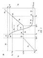
- FIG. 7 The above-mentioned power-saving concept is illustrated in graph 280 of FIG. 7 , which includes a plot of V GS (on the left-hand y-axis) and V DS (on the right-hand y-axis) versus the gate charge Q G (on the x-axis).
- the solid lines indicate the ranges of the gate and drain voltages in a device operated in accordance with this invention, while the solid and dashed lines together indicate the same ranges in a device operated using conventional gate drive techniques. Specifically, in a conventional gate drive, the gate charge starts at zero and then increases along curves 281 , 282 , 283 , and 284 to point 287 .
- the method of this invention can be represented as a plot of Q G versus time as illustrated in graph 320 of FIG. 9 , where the charge present on the MOSFET's gate varies alternates between a magnitude Q GL (curve 321 ) and a magnitude Q GH (curve 323 ) with charging and discharging transitions 322 and 324 . Since some minimum amount of charge Q GL is always left on the device's gate, the charge represented by the area 325 is preserved from one cycle to the next, and the efficiency of the gate drive is improved accordingly.
- the drain voltage V DS varies from point 296 to point 294 along curve 292 , skipping cutoff operation regions, represented by curves 290 and 291 .
- the voltage across the power MOSFET is given by I D ⁇ R Ds(on) .
- FIG. 8 The relationship between current I D and drain voltage V DS is further illustrated in FIG. 8 , where a switching waveform 303 for a switching converter such as Buck converter 1 is overlaid on the MOSFET's family of I-V curves representing gate voltages V GS0 through V GS5 .
- the current increases along curve 302 with V GS while the MOSFET's gate is biased in its saturation region 305 and V DS is relatively constant.
- V GS3 Under gate voltage V GS3 , represented by I-V curve 306 , the drain voltage V DS changes along curve 303 until the MOSFET is operating in its linear operating region 307 , when V DS continues to decline along curve 304 but I D does not change substantially.
- the gates discharge process transitions between the two same end points 301 and 304 in the reverse direction.
- the total conduction loss in the power MOSFET is then the sum of conduction loss P cond when the MOSFET is biased fully on in its linear region and power loss P BIAS due to the bias current I DBIAS during the interval t sat when the MOSFET is in its saturated region of operation, or
- P′ cond I D 2 ⁇ R DS(on) ⁇ D+I DBIAS ⁇ V DD ⁇ (1 ⁇ d )
- P loss ′ [ I D 2 ⁇ R DS ⁇ ( on ) ⁇ t on T + Q GH ⁇ V GH ⁇ 1 T ] + ( I DBIAS ⁇ V DD ⁇ t sat T ) - ( Q GL ⁇ V GL ⁇ 1 T ) where the square bracketed terms represent the gate drive and conduction loss P loss using conventional gate drive techniques. Substituting this term yields the relation
- P loss ′ [ P loss ] + ( I DBIAS ⁇ V DD ⁇ t sat T ) - ( Q GL ⁇ V GL ⁇ 1 T ) where T may vary cycle-to-cycle in variable frequency operation or for fixed frequency operation
- P′ loss [P loss ]+( I DBIAS ⁇ V DD ⁇ (1 ⁇ D )) ⁇ ( Q GL ⁇ V GL ⁇ f )
- V out /V in 1/(1 ⁇ D) where D reflects the on-time of low-side MOSFET 31 .
- Rearranging and substituting V in /V out for (1 ⁇ D) gives us the boost regulator specific condition when the disclosed reduced gate drive method is beneficial
- the disclosed method is more beneficial when a larger output voltage is generated from a lower input voltage.
- the gate drive circuitry “overdrives” the MOSFET to gate bias 294 despite the minimal benefit in reducing on-resistance or voltage drop. Preventing gate overdrive is not easily accomplished since partial charging of the MOSFET's gate to any voltage less than V cc causes the same power loss to occur elsewhere in the circuit and does not improve efficiency.
- FIG. 10 illustrates another embodiment in accordance with this invention.
- extended periods of time may occur when a power MOSFET is not switching, e.g. when a computer is in standby or sleep mode.
- any conduction current, even small amounts like I BIAS flowing from the battery through the load and power MOSFET will discharge the battery over time.
- the solution to the problem of extended off times is to modify the disclosed invention to include a shutdown mode.
- Circuit 350 illustrates a generic description of the disclosed power MOSFET with reduced gate drive loss augmented with an added feature of a shutdown mode. Similar to the circuit 200 of FIG. 5 , circuit 350 includes a gate driver 352 but in this case gate driver 352 has not two, but three states, i.e. fully-conducting with a low-resistance, saturated and biased at V BIAS to conduct a small fixed current, and fully-off for low-leakage cutoff. Accordingly gate driver 352 has two inputs, IN for receiving logic or PWM signals, and an enable pin for shutting the device off.
- the output of buffer 351 feeds the “IN” input terminal of gate driver 352 with a signal ranging from V cc to ground, i.e. a digital signal switching from rail-to-rail. So long that enable is biased into its “on” state, gate driver 352 responds to the signal at its “IN” terminal, and the output of gate driver 352 drives the gate of MOSFET 353 at a voltage V GS1 alternating between V cc and V BIAS . Power MOSFET 353 in turn provides load 354 with a current that alternates between high and low drain currents determined by the gate drive voltages V cc and V BIAS .
- the drain current in power MOSFET 353 is then reduced to the device's I DSS leakage, the junction leakage from drain to source with the gate tied to its source.
- I DSS is even smaller, preferably below one microampere or even several orders of magnitude less than I BIAS .
- FIGS. 11A-11F The three conditions are illustrated and contrasted in FIGS. 11A-11F and summarized in Table 2 below:
- the drain current I D is relatively “constant,” meaning its shows minimal dependence of the value of V DS . It depends strongly however on the gate bias V BIAS .
- N-channel MOSFET 353 is an enhancement device with a positive threshold voltage, i.e. V tn >0
- the device is in cut-off, where the off-state drain current I DSS is due to junction leakage as illustrated in FIG. 11F .
- the leakage current at point 386 for a reverse bias of V DD appears to be zero
- the actual I DSS leakage current plotted on a semi-log graph may show some voltage dependence, but generally it remains well below 1 ⁇ A over the power MOSFET's specified drain voltage range.
- Table 2 reveals that when enable is biased into a high state, the power MOSFET's conduction depends on the logic input IN but when enable is low, the MOSFET is off and operates independent of the IN signal.
- the output conductance g DS ⁇ dI D /dV DS is included as a qualitative measure of drain voltage sensitivity.
- the output V GS of the gate driver driving MOSFET 353 alternates between V cc and V BIAS , as shown by the square wave 411 , 412 , 413 and 414 in graph 410 of FIG. 12A and follows the logic input voltage transitions 404 , 405 , 406 and 407 shown by the arrowed lines of graph 400 .
- the enable signal EN shown by the dotted line remains high at V cc (curve 401 ).
- the drain current I D switches from I DBIAS to V DS /R DS(on) , as shown by the square wave 421 , 422 , 423 and 424 , and as shown in graph 430 , the drain voltage V DS alternates between (V DD ⁇ V) and I D ⁇ R Ds(on) with a waveform 431 , 432 , 433 , and 434 .
- the enable signal V EN is pulled low (curve 402 ) and biased at zero volts (curve 403 ), driving V GS down (curve 415 ) to zero volts (curve 416 ), a gate voltage lower than V BIAS .
- the drain current I D drops (curve 425 ) to a near zero leakage current of magnitude I DSS (curve 426 ).
- V DS jumps (curve 435 ) to a voltage V DD illustrated by curve 435 , slightly higher than the maximum drain voltage (V DD ⁇ V), shown by curve 434 , during the switching of MOSFET 353 .
- gate driver 352 may alternate between two different switching waveforms as illustrated in FIG. 12B . As shown in graph 440 , before time t 1 the voltage output of gate driver 352 alternates between V cc and V BIAS . During low Q G gate drive operation (region 441 ) in a gate driver in accordance with this invention, the minimum gate drive is the bias voltage V BIAS >0 (curve 442 ).
- circuit 350 can be altered dynamically to facilitate conventional rail-to-rail gate drive (region 443 ), where at ti the gate voltage V GS alternates between V cc and ground (curve 444 ). The benefit of reduced gate charge swing is lost during the rail-to-rail interval.
- the MOSFET's gate is grounded 445 for some indefinite time corresponding to the sleep mode.
- circuit 350 can be operated to reduce turn-on related noise.
- region 447 during each turn-on transition the gate voltage in first briefly raised to V BIAS for a short duration (curve 448 ) before being driven to V cc (curve 449 ).
- the stair-stepped gate waveform of curves 448 and 449 reduces the slew rate of the waveform at the drain of MOSFET 353 and can beneficially reduce noise.
- FIG. 13A-13E illustrate several circuits for implementing a power MOSFET gate drive with reduced drive losses.
- a complementary MOSFET gate driver comprising a high-side P-channel MOSFET 451 and low-side N-channel MOSFET 453 drives the gate of a power MOSFET 454 .
- An N-channel pass transistor 452 also connects the gate of MOSFET 454 to V ref , a reference voltage provided by a reference voltage source 455 .
- the gate voltage on MOSFET 452 must be sufficiently positive relative to its source voltage to turn on MOSFET 452 . Controlled by appropriate timing and logic circuitry, only one device is turned on at a time.
- V GS V batt and MOSFET 454 is operating in its linear region.
- MOSFET 452 As shown, the body of MOSFET 452 is grounded. The grounded body is needed to prevent parasitic diode conduction in MOSFET 452 , since depending on the state of MOSFETs 451 and 453 the gate voltage V GS may be either greater than or less than the value of V ref .
- the parasitic body diodes 457 A and 457 B remain permanently reverse-biased. If the body of MOSFET 452 is not grounded, but instead incorporates a source-body short, then one of these diodes would be in parallel with the channel of MOSFET 452 , similar to diode 456 in parallel with MOSFET 454 .
- a source-to-drain parallel diode would become forward biased in one of the various gate bias conditions, namely when V GS >V BIAS or when V GS ⁇ V BIAS .
- pass transistor 462 contains parasitic P-N diodes 469 A and 469 B.
- a network of two cross-coupled N-channel MOSFETs 468 A and 468 B bias the body potential of MOSFET 462 so that whichever diode becomes forward biased, it is shorted out by a parallel MOSFET, leaving the other parasitic diode reverse-biased and non-conducting.
- diode 469 B is forward-biased and diode 469 A is reverse biased. Since V GS is the more positive terminal, N-channel MOSFET 468 B turns-on and shorts out the forward-biased diode 469 B, tying the body of MOSFET 462 to its more negative V BIAS terminal, turning off MOSFET 468 A, and leaving diode 469 A reversed-biased and in parallel with MOSFET 462 . As a symmetrical circuit, whenever the polarity reverses the devices switch state and diode 469 B becomes reverse-biased and parallel to pass transistor 462 .
- the body bias generator technique can be applied to any pass transistor, e.g. in circuit 450 .
- a pass transistor is defined herein as a MOSFET with neither source nor drain connected to a fixed supply rail.
- circuit 460 is Similar to circuit 450 except that a digital-to-analog converter 465 is substituted for fixed voltage reference 455 .
- the output of the D/A converter 465 allows V BIAS to be adjusted using digital control of D/A converter 465 .
- D/A converter 465 outputs a voltage up to a maximum amount V ref supplied by a voltage reference source 466 .
- circuit 460 of FIG. 13B utilizes a complementary MOSFET gate driver comprising a high-side P-channel MOSFET 461 and a low-side N-channel MOSFET 463 driving the gate of power MOSFET 464 whenever N-channel pass transistor 462 is off.
- FIG. 13C illustrates an implementation of a D/A converter-driven power MOSFET with low-drive losses made in accordance with this invention.
- the gate of a power MOSFET 471 is powered by a multiplexer comprising N-channel and/or P-channel pass transistors 472 , 473 , 474 and 475 , only one of which may conduct at a time.
- the body bias techniques described above may be employed as needed.
- FIG. 13D illustrates another D/A converter driven power MOSFET, where the bias conditions are determined by a resistor-divider network comprising resistors 496 A, 496 B, and 496 C to produce bias points V G2 and V G1 .
- a combination of forward-biased diodes and resistors may also be used, as shown in FIG. 13E .
- the divider network need not comprise linear steps, but can include greater resolution near the targeted bias voltage. All of the D/A converter gate drive methods described provide some degree of control in setting the value of I DBIAS either during manufacturing or during operation.
- FIG. 14A illustrates a circuit 550 for implementing the gate driver 202 shown in FIG. 5 .
- the gate of power MOSFET 556 is driven by a CMOS driver comprising high-side P-channel MOSFET 553 connected to V cc and N-channel MOSFET 554 with its source biased to reference voltage V BIAS provided by a voltage source 555 .
- V GS1 V BIAS
- I D the drain current I D is proportional to (V BIAS ⁇ V t ). Since V t varies with temperature and with manufacturing from lot-to-lot, then the current will vary accordingly.
- circuit 580 in FIG. 14B includes I D current feedback circuit 90 which dynamically adjusts the value of the reference voltage V BIAS provided by reference voltage source 585 using an amplifier 588 to force the drain current I D to a multiple of the reference current I ref provided by current source 589 .
- the magnitude of the drain current is measured by a current sensor 590 and delivered to the negative input of amplifier 588 .
- the feedback stabilizes the output current. For any increase in current I D , the negative input to amplifier 588 decreases its output, lowering the magnitude of V BIAS and decreasing I D , thereby offsetting the current increase.
- I D drain current feedback is achieved using a sense resistor 615 B.
- the voltage drop Vs across resistor 615 B is amplified differentially by an operational amplifier 618 with respect to a reference voltage V REF provided by voltage source 619 to produce the voltage V BIAS .
- the bias voltage V BIAS drives the gate of power MOSFET 616 Whenever MOSFET 614 is biased in an on-state condition.
- Current sense resistor 615 B increases the total resistance in series with electrical load 617 and therefore reduces efficiency.
- an improved circuit 620 utilizes a current mirror comprising a power MOSFET 626 A with a gate width n ⁇ W and a sense MOSFET 626 B with a gate width W, having common gate and source terminals and separate drain connections.
- a CMOS gate driver comprising a P-channel MOSFET 623 and an N-channel MOSFET 624
- power MOSFET 626 A controls the current I D through load 629 .
- An operational amplifier 628 controls the current in current-source 627 , forcing the drain voltage V ⁇ of MOSFET 626 B to the same voltage as the drain of power MOSFET 626 A.
- the sense current I sense 627 is mirrored to a current source 630 and Converted into a voltage V sense across a sense resistor 631 . Unlike resistor 615 B in circuit 610 , sense resistor 631 does not contribute to increased resistance in series with load 629 .
- current-mirror circuit 620 over circuit 610 is that it doesn't introduce any additional voltage drop in series with the electrical load 629 , and therefore improves energy transfer efficiency from the power source to load 629 .
- the current mirror method embodied in circuit 620 can be used only with common-source split-drain MOSFETs such as MOSFETs 626 A and 626 B, where the drains of the MOSFETs can be separately connected. It cannot be used with common-drain devices current in discrete power MOSFET 656 without introducing a such as trench-gated vertical DMOS or planar vertical DMOS.
- circuit 650 shown in FIG. 15C may be employed to accurately monitor the drain current in discrete power MOSFET 656 without introducing a large-value sense resistor in series with load 657 .
- the sense current 660 is then used to control the magnitude of I DB1As during low current conduction and to sense short-circuit conditions in the high-current low-resistance state.
- This current sensing method is described in application Ser. No. 11/890,948, titled “Cascode Current Sensor For Discrete Power Semiconductor Devices,” filed contemporaneously herewith and incorporated herein by reference.
- the gate bias applied to power MOSFET 656 is controlled by a gate driver comprising a P-channel 653 MOSFET and an N-channel MOSFET 654 .
- the gate potential V GS may comprise either V cc when operating in a low-resistance condition, or V BIAS in the low-current state.
- the voltage V BIAS is controlled using feedback to produce a desired output current I DBIAS regardless of operating conditions or manufacturing process variations.
- Current sensing is achieved using a low-resistance low-voltage MOSFET 658 A with gate width n ⁇ W connected in series with power MOSFET 656 .
- Power MOSFET 656 may comprise a low or high-voltage device and need not be integrated with the other components in circuit 650 .
- the current sensing element includes a current mirror MOSFET 658 B of gate width W fabricated monolithically with the larger MOSFET 658 A and sharing a common source and split drain.
- both MOSFETs 658 A and 658 B have their gates biased to the supply voltage V cc and are therefore biased into their low-resistance linear-regions of operation. Even at high I D drain currents, the low-resistance of MOSFET 658 A insures that voltage V ⁇ at the drain of MOSFET 658 A remains low.
- the drain voltage of MOSFET 658 B is designated V ⁇ .
- the value of I sense is mirrored using a current mirror 661 into a proportional current I mirror in series with a sense resistor 664 to produce a sense voltage V sense proportional to V ⁇ . Because of the voltage gain of operational amplifier 659 , the signal V sense can be made large despite the fact that the voltage V ⁇ is small.
- the value of V sense is amplified differentially by an operational amplifier 663 with respect to a reference voltage V BIAS produced by a voltage source 662 .
- the value of drain current I DBIAS can be accurately controlled.
- the minimum gate charge Q GL remaining on a power MOSFET's gate in the low state of each switching cycle can also be controlled consistent with the graph of FIG. 9 and in accordance with the inventive method to minimize gate drive losses.
- a power MOSFET gate driver 701 drives the gate of a power MOSFET 702 with a voltage alternating between V cc for low-resistance operation and V BIAS for low-current conduction.
- a fixed voltage source 706 sets the value of V BIAS .
- the current I D is measured by test equipment and used to adjust a trim network 705 until the measured value of I D matches the target value of the bias current I DBIAS . This calibration is preferably performed at room temperature.
- an optional temperature compensation circuit 709 can be used to adjust V BIAS 706 to maintain a semi-constant value of I D over temperature.
- a trimmed gate drive circuit 720 shown in FIG. 16B , includes a gate driver with MOSFETs 721 and 722 , a power MOSFET 724 , and a load 725 .
- the remaining components are used to implement the trimmed bias voltage V BIAS , including a reference voltage source 726 providing a reference voltage V ref , a resistor divider network 728 , including resistors 728 A and 728 B and 729 a - 729 e, one time programmable (OTP) MOSFETs 730 a - 730 e , bias multiplexers 731 a - 731 e and an OTP programmer 727 .
- Resistors 728 A and 728 B have values R A and R B , respectively.
- OTP MOSFETs 730 a - 730 e exhibit normal threshold Voltages well below V cc .
- multiplexers 731 a - 731 e bias the gate of each of OTP MOSFETs 730 a - 730 e to V cc , turning each of OTP MOSFETs 730 a - 730 e on and shorting out the one of resistors 729 a - 729 e with which it is connected in parallel.
- OTP MOSFET 730 c has a threshold of 0.7V.
- multiplexer 731 c connects the gate of OTP MOSFET 730 c to V cc , then it conducts and shorts out corresponding resistor 729 c.
- V BIAS ( R A R A + R B ) ⁇ V ref
- Programming involves connecting the gate of any given one of OTP MOSFETs 730 a - 730 e to programmer 727 , and biasing the device into saturation at high voltages.
- the process creates hot carriers and charges the gate oxide permanently increasing the threshold voltage of the device to a higher value so that under normal operation the OTP MOSFET will not conduct.
- the parallel one of resistors 729 a - 729 e is thereby inserted into voltage divider 728 , adjusting the resistor divider ratio and the value of V BIAS .
- the values of resistors 729 a - 729 e may be equal or different, so that trimming may be linear or non-linear.
- the trimmed output can range from as high as V ref to some fraction V ref /m.
- the codes may be arranged in any number of combinations, such as those shown in FIG. 16C .
- codes C 1 to C 8 correspond to various resistor combinations depending on which resistors are shorted by un-programmed OTP MOSFETs 730 a - 730 e .
- the code C 1 starts with V BIAS at the lowest voltage (line 741 ) and increases (line 742 ) as various bits are programmed by turning off individuals ones of OTP MOSFETs 730 a - 730 e.
- An alternative pattern, indicated by line 743 uses non-linear steps and ends with a maximum voltage (line 744 ) of magnitude V ref .
- a general programming algorithm 780 for trimming V BIAS is shown in FIG. 16D , where a fixed voltage V DS is applied to power MOSFET 724 operated in its low-current, i.e. I DBIAS , state.
- the drain current I D is measured in step 782 , and in step 783 the drain current I D is compared to a target range of I DBIAS within some tolerance. If the current is too low, one or more of OTP MOSFETs 730 a - 730 e are programmed in step 784 , increasing V BIAS and the current I D .
- the process is then repeated (step 785 ), until the measured I D reaches the specified range for I DBIAS and then the program terminates (step 786 ).
- I DBIAS programming An example of I DBIAS programming is shown in FIG. 16E , where a product after manufacture has a current of magnitude I initial (line 801 ) and during each iteration the current increases until it reaches a value represented by line 802 , just outside the target range of I Dlow to I Dhigh . In the fifth iteration the current increases to a value represented by line 804 , which is within the target range, and the program is then terminated. While the program may be performed at room temperature, the same program may also be used at higher temperatures.
- Temperature compensation circuit 709 in FIG. 16A may assume a certain temperature coefficient, e.g. at ⁇ 3 mV/° C. to avoid the need for trimming at high temperatures. Either way, the accuracy of I DBIAS is improved using trimming, and therefore more tightly controls the gate charge swing of MOSFET 702 .
- I DBIAS the magnitude of I DBIAS depends on the power MOSFET's threshold. In one case, active trimming was employed to adjust the value of V BIAS to produce a targeted value of I DBIAS . In the other case, current feedback was employed to force I D to a target value I DBIAS under closed loop operation.
- a reduced gate drive loss circuit utilizes a gate drive technique insensitive to threshold fluctuations in the power MOSFET.
- One such method to eliminate sensitivity to threshold utilizes the current-mirror gate drive circuit 820 shown in FIG. 17A . Without actually sensing the current, the technique employs the principle that two MOSFETs fabricated monolithically will exhibit substantially matched threshold voltages and under identical gate drive conditions, in saturation the drain currents will scale roughly in proportion to MOSFET gate width.
- MOSFETs 824 A and 824 B are fabricated monolithically as a current mirror 830 .
- Power MOSFET 824 A is a low-resistance device with a large gate width n ⁇ W, while current mirror MOSFET 824 B has a gate width of W—a factor of “n” smaller than the gate width of MOSFET 824 A.
- the gate of MOSFET 824 A is driven by gate driver 821 with options of selecting among three inputs—V cc , V BIAS and ground. When V cc is selected, power MOSFET 824 A is biased into a low-resistance state, operating in its linear region. When ground is selected, power MOSFET 824 A is cut off and no current flows.
- the gate drive of power MOSFET 824 A is determined by a bias network comprising a current source 822 and mirror MOSFET 824 B.
- the equivalent circuit in this mode is shown in FIG. 17B , where a fixed current source 822 is chosen or preset to supply the target current I DBIAS divided by the width ratio “n”.
- This current I DBIAS /n is fed into MOSFET 824 B having its drain and gate shorted, i.e. threshold-connected.
- Threshold-connected MOSFET 824 B is self biasing, meaning it will adjust its gate voltage to a potential V BIAS needed to carry the drain current supplied by fixed current source 822 .
- V BIAS voltage the gate voltage of MOSFET 824 B, is also the gate voltage on large power MOSFET 824 A.
- trim circuit 831 can be employed to adjust the value of current source 822 as part of the manufacturing process.
- Gate drive circuit 860 without trimming is shown in FIG. 18 .
- Gate drive circuit 860 comprises a current-mirror MOSFET pair 861 , a load 863 , a tri-state gate drive including MOSFETs 864 , 865 and 870 , a break-before-make (BBM) buffer 866 and a bias current generator MOSFET pair 871 with a resistor 869 .
- power MOSFET 862 A may be biased into a low-resistance state when P-channel MOSFET 864 is on, into a fully-off non-conducting state when N-channel MOSFET 870 is on and into saturation at a low controlled current I DBIAS when N-channel MOSFET 865 is on.
- BBM buffer 866 only one of MOSFETs 864 , 865 and 870 may be on at one time.
- MOSFET pair 861 comprises power MOSFET 862 A with gate width n ⁇ W and smaller current mirror MOSFET 862 B with gate width W. With voltage V BIAS on the gate and drain of MOSFET 862 B, the device conducts a drain current I DBIAS /n. This current is established by current mirror 871 comprising P-channel MOSFETs 867 and 868 . Threshold-connected MOSFET 868 conducts a current I ref set by resistor 869 , having a magnitude of
- I ref V cc - V tp R ⁇ I DBIAS n
- the current I ref is mirrored by MOSFET 867 to drive MOSFET 862 B.
- the value R of resistor 869 is adjusted to set this current to a target value I DBIAS /n.
- FIG. 19 illustrates a current-mirror gate drive 880 made in accordance with this invention, wherein I ref is implemented using a voltage reference source 890 providing a voltage V ref and a resistor 889 .
- the current I ref is then given by
- Circuit 880 also illustrates another implementation of a tri-state gate driver.
- the gate driver comprises a V cc -connected P-channel MOSFET 884 , a V BIAS -connected N-channel MOSFET 885 and ground-connected N-channel MOSFET 891 being driven by logical “AND” gates 892 and 893 and by inverters 894 , 895 , and 896 .
- enable signal EN is a logic low state
- the output of AND gates 892 and 893 are low turning MOSFET 885 off, and inverted by inverter 894
- the output of AND gate 892 biases the gate of P-channel MOSFET 884 high, turning it off.
- the low enable signal inverted by inverter 896 drives ground MOSFET 891 with a high gate bias, turning it on and shorting the gate of power MOSFET 882 A to ground. In such a state, MOSFET 891 is on and MOSFETs 884 and 885 are off.
- inverter 896 When enable EN is high, the output of inverter 896 is low and MOSFET 891 is off. With EN as a high input to AND gates 892 and 893 , their outputs depend solely on the state of the input pin IN.
- inverter 895 drives the input and output of AND gate 893 low and turns off N-channel MOSFET 885 .
- a high input drives the input and output of AND gate 892 high and inverted by inverter 894 , the gate of P-channel MOSFET 884 low, turning on P-channel 884 . In such a state, MOSFET 884 is on and MOSFETs 885 and 896 are off.
- inverter 895 drives the input and output of AND gate 893 high and turns on N-channel MOSFET 885 .
- a low input drives the input and output of AND gate 892 low and inverted by 894 , the gate of P-channel MOSFET 884 high, turning off P-channel 884 .
- MOSFET 885 is on and MOSFETs 884 and 896 are off.
- Circuit 880 therefore operates as a tri-state gate driver to control the conduction and gate charge swing of power MOSFET 882 A in accordance with this invention.
- Table 3 is a truth table for the tri-state gate driver's logic.
- FIG. 20 Another variant of current-mirror gate driver in accordance with this invention is illustrated in FIG. 20 , where a tri-state gate driver 901 drives the gate of a power MOSFET 903 A with a value V GS1 to one of three potentials—V cc , ground, or V BIAS .
- the voltage V BIAS is determined by threshold-connected MOSFET 903 B conducting a current I ref from a controlled current source 904 .
- MOSFETs 903 B and 903 A together comprise a monolithically fabricated MOSFET pair 902 with gate widths W and n ⁇ W, respectively.
- the current I ref is adjusted by a D/A converter 906 under control of a digital logic, digital signal processor, or microprocessor 907 and may be adjusted dynamically and in real time as desired.
- D/A converter 906 and dependent current source 904 together may comprise a current-output D/A converter.
- FIG. 21B An example of a current-type D/A converter 947 directly driving a mirror MOSFET 942 B is illustrated in FIG. 21B .
- Current-mode D/A-converter 947 includes a reference voltage source 949 generating a reference voltage V ref to eliminate sensitivity to fluctuations in the supply voltage V cc .
- the current I ref may be generated, as shown in FIG. 21A , using a D/A converter 929 controlling a controlled voltage source 928 .
- the precise value of R may be trimmed using a series of resistors and OTP MOSFETs as described previously.
- I DBIAS drain current I Dsat during saturation
- I DBIAS can be adjusted in response to changing conditions.
- FIG. 22A illustrating I DBIAS versus I Dlin .
- Curve 983 in graph 980 illustrates a constant percentage controlled using analog feedback of the linear region current.
- a stair stepped increase in I DBIAS comprising currents shown as curves 982 a , 982 b and 982 c can be achieved using a D/A converter and digital control.
- a constant I DBIAS is shown as line 981 for reference.
- I DBIAS is varied (curve 992 ) as a function of frequency f rather than remaining constant (line 991 ).
- FIG. 23A An alternative approach, illustrated in FIG. 23A , is to switch the gate bias on current mirror MOSFET 1002 B between ground and a bias supply current I ref during high frequency switching.
- a gate driver 1005 connects the gate of N-channel MOSFET 1002 B to ground, turning off MOSFET 1002 B.
- V GS1 V cc
- power MOSFET 1002 A is biased into a low-resistance state, during which MOSFET 1006 remains off.
- gate driver 1005 connects the gate of MOSFET 1002 B to V cc turning it on and grounding the gate of power MOSFET 1002 A. In this condition, MOSFETs 1004 and 1006 remain off.
- switched bias circuit 1000 requires only two large area MOSFETs as buffers to drive the gate of power MOSFET 1002 A, namely high-side MOSFET 1004 to drive power MOSFET 1002 A into a low resistance state, and multifunction mirror MOSFET 1002 B to provide V BIAS gate drive for operation of power MOSFET 1002 A in saturation and to turn off power MOSFET 1002 A.
- FIG. 23B illustrates a version of circuit 1000 wherein the gate driver driving the gate of current mirror MOSFET 1022 B comprises a grounded N-channel MOSFET 1025 for turning MOSFET 1022 B off, and an N-channel MOSFET 1029 for shorting the gate and drain of MOSFET 1022 B.
- MOSFET 1026 is employed to bias the gate of mirror MOSFET 1022 B at a voltage V BIAS .
- MOSFET 1024 is used to drive power MOSFET 1022 A into a low resistance state.
- FIGS. 24A-24D illustrate low-loss gate drives using N-channel power MOSFETs
- FIGS. 25A and 25B illustrate low-loss gate drives using P-channel and complementary power MOSFETs.
- the gate driver may comprise a two-state driver switching between a low-resistance fully-on condition, and a limited-current saturated-MOSFET condition.
- the gate driver may comprise a tri-state buffer switching between a low resistance fully-on condition, a limited current saturated-MOSFET condition, and a fully-off condition for sleep mode operation.
- Each power MOSFET in a power circuit may employ one of the low gate drive loss techniques or alternatively only one of the power devices may utilize the low-drive-loss method.
- FIG. 24A illustrates a tri-state gate driver 1102 with a voltage supply 1106 generating V BIAS and powered by a voltage supply 1105 generating V cc driving a grounded, i.e. low-side configured, N-channel power MOSFET 1101 .
- Voltage supplies 1104 (V DD ) and 1105 (V cc ) may comprise the same power supply.
- FIG. 24B illustrates floating tri-state gate driver 1122 with a floating voltage supply 1126 generating V BIAS powered by a bootstrap capacitor 1128 driving a high-side, i.e. source-follower configured, N-channel power MOSFET 1121 .
- Bootstrap capacitor 1128 is charged by a voltage supply 1125 generating V cc through a bootstrap diode 1127 whenever MOSFET 1121 is off and a voltage V x at a load 1123 is at ground or less than the supply voltage V cc .
- the current in power MOSFET 1121 and load 1123 may be equal to V DD /R when MOSFET 1121 is in a low-resistance state, a constant current I DBIAS when MOSFET 1121 is in saturation, or zero when MOSFET 1121 is not switching.
- the switching of MOSFET 1121 is inhibited when the enable signal EN is low and the gate of power MOSFET 1121 is connected to its source voltage V x .
- the enable and input signals are level-shifted by a level-shift circuit 1129 feeding gate driver 1122 .
- the voltage supplies 1124 (V DD ) and 1125 (V cc ) may be a single voltage supply.
- FIG. 24C illustrates a synchronous boost converter 1160 comprising a low-side N-channel power MOSFET 1161 , a synchronous rectifier MOSFET 1166 , and low loss gate drivers 1162 and 1167 in accordance with this invention.
- tri-state gate driver 1162 with a voltage supply 1163 generating V BIASL is powered by V batt and drives a grounded, low-side configured, N-channel power MOSFET 1161 .
- the current in power MOSFET 1161 may be equal to V x /R when MOSFET 1161 is in a low-resistance state, a constant current I DBIAS when MOSFET 1161 is in saturation, or zero when MOSFET 1161 is not switching.
- PWM pulse-width modulation
- Boost converter 1160 also illustrates a P-N rectifier diode 1169 which conducts whenever low-side MOSFET 1161 is off and V x flies above V out .
- a floating N-channel synchronous rectifier MOSFET 1166 conducts some portion of the time when low-side MOSFET 1161 is off.
- synchronous rectifier MOSFET 1166 is driven by a two-state gate driver 1167 , and powered by a bootstrap capacitor 1172 .
- Bootstrap capacitor 1172 is charged from V batt through a bootstrap diode 1171 whenever V x is near ground.
- V boot floats on top of V x so that the supply to gate driver 1167 is V boot ⁇ (V batt ⁇ V f ) regardless of the magnitude of the voltage V x .
- V f is the forward-bias voltage across bootstrap diode 1171 while charging bootstrap capacitor 1172 .
- the synchronous rectifier MOSFET 1166 is preferably driven out of phase with low-side MOSFET 1161 by inverting break-before-make buffer 1173 so that only one MOSFET at a time is operating in a low-resistance high-current state.
- the other MOSFET may be off or conducting a low bias current I DBIAS to reduce gate charge swing in accordance with this invention.
- N-channel MOSFET 1161 exhibits a larger drain voltage transition during conduction than synchronous rectifier MOSFET 1166 , the benefit of the invention limiting the gate charge swing is greatest for gate driver 1162 driving low-side MOSFET 1161 . Nonetheless, driver 1167 driving synchronous rectifier MOSFET 1166 provides some reduction in gate drive losses and more importantly reduces the efficiency loss and noise generated from diode recovery in rectifier diode 1169 .
- Table 4 is a truth table describing the various combinations described above.
- MOSFET 1161 forms a series shunt from the battery input to ground.
- Putting MOSFET 1166 into a sleep mode wherein the switching of MOSFET 1166 is inhibited does not prevent V batt from charging output capacitor 1170 to approximately V batt since diode 1169 is forward biased whenever V batt >V out .
- the main benefit of putting synchronous rectifier MOSFET 1166 into a sleep mode is to prevent a gradual discharge of capacitor 1170 back into V batt .
- Buck converter 1180 comprises a floating tri-state gate driver 1182 with a floating voltage supply 1183 generating V BIASH .
- Gate driver 1182 is powered by a bootstrap capacitor 1185 and drives a high-side, i.e. source-follower configured, N-channel power MOSFET 1181 .
- Bootstrap capacitor 1185 is charged from V batt through a bootstrap diode 1184 whenever MOSFET 1181 is off and voltage V x is at ground or less than the supply voltage V batt .
- MOSFET 1181 has its on-time controlled by a PWM controller 1193 .
- the width of the pulses supplied to MOSFET 1181 is modulated to control the current flowing through inductor 1190 and charging capacitor 1191 .
- the output voltage V out is fed back to PWM controller 1193 , using a feedback signal V FB , to regulate the output voltage against variations in the input voltage V batt and load current.
- inductor 1190 forces V x below ground, and as a result diode 1189 becomes forward-biased.
- a low-side N-channel MOSFET 1186 is included to reduce diode conduction losses by shunting current through a lower voltage drop path whenever gate driver 1187 biases the gate of MOSFET 1186 to V batt .
- high-side MOSFET 1181 exhibits a larger drain voltage transition during conduction than synchronous rectifier MOSFET 1186 , the benefit of the invention in limiting the gate charge swing is greatest for gate driver 1182 driving high-side MOSFET 1181 . Nonetheless, gate driver 1187 driving synchronous rectifier MOSFET 1186 provides some reduction in gate drive losses and more importantly reduces the efficiency loss and noise generated from diode recovery in rectifier diode 1189 .
- gate driver 1182 need be tri-state since turning off either MOSFET 1181 or 1186 breaks the current path from V batt to ground.
- FIG. 25A in circuit 1200 illustrates a tri-state gate driver 1202 with a voltage supply 1203 generating V BIAS .
- a voltage supply 1205 generating V DD drives a load 1204 via a V cc -connected, i.e. high-side configured, P-channel power MOSFET 1201 .
- the current in power MOSFET 1201 and load 1204 may be equal to V DD /R in a low resistance state of MOSFET 1201 , a constant current I DBIAS when MOSFET 1201 is in saturation, and zero when MOSFET 1201 is not switching.
- the switching of MOSFET 1201 is inhibited when an enable signal EN is low and the gate of power MOSFET 1201 is connected to V DD .
- the enable (EN) and input (IN) signals may be delivered to logic switching between V DD and ground, as indicated by inverters 1206 and 1209 , which are biased between V cc and ground. If the supply voltage V DD is greater than V cc the EN and IN signals must be level-shifted to V DD .
- the level shift circuit employs an N-channel MOSFET 1207 and a resistor 1208 to convert the output of inverter 1206 into an input signal IN′ switching between V DD and ground.
- an N-channel MOSFET 1210 and resistor 1211 convert the output of inverter 1209 into an enable signal EN′ switching between V DD and ground.
- V cc and V DD may be supplied by a single power supply so that level-shift circuitry is not required.
- Converter 1220 comprises a high-side referenced tri-state gate driver 1222 with a high-side referenced voltage supply 1223 generating V BIASH powered directly by V batt and driving a high-side, i.e. common-source configured, P-channel power MOSFET 1221 .
- MOSFET 1221 The on-time of MOSFET 1221 is controlled by a PWM controller 1231 .
- the width of the pulses delivered to the gate of MOSFET 1221 is modulated to control the current flowing through an inductor 1228 , charging a capacitor 1229 .
- the output voltage V out is fed back to PWM controller 1231 using a feedback signal V FB to regulate the output voltage against variations in the input voltage and load current.
- inductor 1228 forces V x below ground, and as a result diode 1227 becomes forward-biased.
- a low-side N-channel MOSFET 1224 is included to reduce diode conduction losses by shunting current through a lower voltage drop path whenever gate driver 1225 biases the gate of MOSFET 1224 to V batt .
- a BBM circuit 1230 prevents MOSFETs 1221 and 1224 from simultaneously conducting high currents.
- P-channel MOSFET 1221 exhibits a larger drain voltage transition during conduction than synchronous rectifier MOSFET 1224 , the benefit of the invention in limiting the gate charge swing is greatest for gate driver 1222 driving high-side P-channel MOSFET 1221 . Nonetheless gate driver 1225 driving synchronous rectifier MOSFET 1224 provides some reduction in gate drive losses and more importantly reduces the efficiency loss and noise generated from diode recovery in rectifier diode 1227 .
- gate driver 1222 need be tri-state since turning off either MOSFET 1221 or 1224 breaks the current path from V batt to ground.
Landscapes
- Engineering & Computer Science (AREA)
- Power Engineering (AREA)
- Dc-Dc Converters (AREA)
- Power Conversion In General (AREA)
- Electronic Switches (AREA)
Priority Applications (10)
| Application Number | Priority Date | Filing Date | Title |
|---|---|---|---|
| US11/890,942 US7812647B2 (en) | 2007-05-21 | 2007-08-08 | MOSFET gate drive with reduced power loss |
| JP2010509331A JP5261777B2 (ja) | 2007-05-21 | 2008-04-30 | 電力損失が低減されたmosfetゲートドライブ |
| PCT/US2008/005543 WO2008153631A1 (en) | 2007-05-21 | 2008-04-30 | Mosfet gate drive with reduced power loss |
| KR1020097026341A KR101222793B1 (ko) | 2007-05-21 | 2008-04-30 | Mosfet 게이트 구동 회로장치 |
| CN201310021711.2A CN103152022B (zh) | 2007-05-21 | 2008-04-30 | 减小功耗的mosfet 栅极驱动器 |
| CN2008800256665A CN101785187B (zh) | 2007-05-21 | 2008-04-30 | 减小功耗的mosfet栅极驱动器 |
| EP08767451A EP2156558A4 (en) | 2007-05-21 | 2008-04-30 | MOSFET GATE CONTROL WITH REDUCED PERFORMANCE LOSS |
| TW097117729A TWI369846B (en) | 2007-05-21 | 2008-05-14 | Mosfet gate drive with reduced power loss |
| US12/924,164 US7994827B2 (en) | 2007-05-21 | 2010-09-22 | MOSFET gate drive with reduced power loss |
| HK13109921.0A HK1182842A1 (zh) | 2007-05-21 | 2013-08-26 | 減小功耗的 柵極驅動器 |
Applications Claiming Priority (2)
| Application Number | Priority Date | Filing Date | Title |
|---|---|---|---|
| US93109707P | 2007-05-21 | 2007-05-21 | |
| US11/890,942 US7812647B2 (en) | 2007-05-21 | 2007-08-08 | MOSFET gate drive with reduced power loss |
Related Child Applications (1)
| Application Number | Title | Priority Date | Filing Date |
|---|---|---|---|
| US12/924,164 Division US7994827B2 (en) | 2007-05-21 | 2010-09-22 | MOSFET gate drive with reduced power loss |
Publications (2)
| Publication Number | Publication Date |
|---|---|
| US20080290911A1 US20080290911A1 (en) | 2008-11-27 |
| US7812647B2 true US7812647B2 (en) | 2010-10-12 |
Family
ID=40071824
Family Applications (2)
| Application Number | Title | Priority Date | Filing Date |
|---|---|---|---|
| US11/890,942 Expired - Fee Related US7812647B2 (en) | 2007-05-21 | 2007-08-08 | MOSFET gate drive with reduced power loss |
| US12/924,164 Expired - Fee Related US7994827B2 (en) | 2007-05-21 | 2010-09-22 | MOSFET gate drive with reduced power loss |
Family Applications After (1)
| Application Number | Title | Priority Date | Filing Date |
|---|---|---|---|
| US12/924,164 Expired - Fee Related US7994827B2 (en) | 2007-05-21 | 2010-09-22 | MOSFET gate drive with reduced power loss |
Country Status (8)
| Country | Link |
|---|---|
| US (2) | US7812647B2 (zh) |
| EP (1) | EP2156558A4 (zh) |
| JP (1) | JP5261777B2 (zh) |
| KR (1) | KR101222793B1 (zh) |
| CN (2) | CN101785187B (zh) |
| HK (1) | HK1182842A1 (zh) |
| TW (1) | TWI369846B (zh) |
| WO (1) | WO2008153631A1 (zh) |
Cited By (13)
| Publication number | Priority date | Publication date | Assignee | Title |
|---|---|---|---|---|
| US20090039869A1 (en) * | 2007-08-08 | 2009-02-12 | Advanced Analogic Technologies, Inc. | Cascode Current Sensor For Discrete Power Semiconductor Devices |
| US20090206785A1 (en) * | 2008-02-15 | 2009-08-20 | Intersil Americas Inc. | Waveform current monitor using rdson of low-side bridge fet |
| US20090300375A1 (en) * | 2008-05-30 | 2009-12-03 | Hong Fu Jin Precision Industry (Shenzhen) Co., Ltd | Power supply control circuit |
| US20100225396A1 (en) * | 2009-03-03 | 2010-09-09 | Kabushiki Kaisha Toshiba | Semiconductor integrated circuit and electronic device |
| WO2012087320A1 (en) * | 2010-12-22 | 2012-06-28 | Hewlett-Packard Development Company, L.P. | Mosfet switch gate driver, mosfet switch system and method |
| US20120169377A1 (en) * | 2010-12-30 | 2012-07-05 | Infineon Technologies Ag | Circuit Arrangement including a Common Source Sense-FET |
| US20130058135A1 (en) * | 2011-09-05 | 2013-03-07 | Filippo Marino | Adaptive Driver Delay Compensation |
| US20130063114A1 (en) * | 2011-09-14 | 2013-03-14 | Texas Instruments Incorporated | Circuits and methods for controlling pwm input of driver circuit |
| US8985850B1 (en) | 2009-10-30 | 2015-03-24 | Cypress Semiconductor Corporation | Adaptive gate driver strength control |
| US9236866B2 (en) | 2012-07-10 | 2016-01-12 | Samsung Electronics Co., Ltd. | Circuit for driving gate of power MOS transistor |
| US11201463B2 (en) | 2020-03-18 | 2021-12-14 | Analog Devices International Unlimited Company | Inductor discharge techniques for switch controller |
| US11387821B2 (en) * | 2020-02-17 | 2022-07-12 | Mitsumi Electric Co., Ltd. | Pulse signal sending circuit |
| WO2023110726A1 (en) * | 2021-12-16 | 2023-06-22 | Signify Holding B.V. | Solar powered battery charger |
Families Citing this family (86)
| Publication number | Priority date | Publication date | Assignee | Title |
|---|---|---|---|---|
| US7876133B1 (en) * | 2006-09-27 | 2011-01-25 | Cypress Semiconductor Corporation | Output buffer circuit |
| US7839131B2 (en) * | 2007-06-27 | 2010-11-23 | International Rectifier Corporation | Gate driving scheme for depletion mode devices in buck converters |
| US20100060257A1 (en) * | 2008-09-05 | 2010-03-11 | Firas Azrai | Current sensor for power conversion |
| US8461880B2 (en) * | 2009-04-02 | 2013-06-11 | Silicon Labs Spectra, Inc. | Buffer with an output swing created using an over-supply voltage |
| US8325453B2 (en) * | 2009-05-28 | 2012-12-04 | Qualcomm, Incorporated | Short-circuit protection for switched output stages |
| EP2299569B1 (de) | 2009-09-21 | 2014-07-16 | BIONIC Engineering 5D+ AG | Gleichspannungsschaltwandler und Gleichspannungsschaltwandlungsverfahren |
| JP5139391B2 (ja) * | 2009-09-25 | 2013-02-06 | 株式会社東芝 | ばらつき分布シミュレーション装置及び方法 |
| US20130006039A1 (en) * | 2010-02-10 | 2013-01-03 | Sadler John W | Power management in transcranial magnetic stimulators |
| DE102010024128A1 (de) * | 2010-06-17 | 2011-12-22 | Diehl Ako Stiftung & Co. Kg | Wechselspannungssteller |
| JP5367651B2 (ja) * | 2010-06-28 | 2013-12-11 | 日立オートモティブシステムズ株式会社 | 電流制御用半導体素子、およびそれを用いた制御装置 |
| US8334683B2 (en) * | 2010-08-24 | 2012-12-18 | Intersil Americas Inc. | System and method for current limiting a DC-DC converter |
| US8680895B2 (en) * | 2010-10-08 | 2014-03-25 | Texas Instruments Incorporated | Controlling power chain with same controller in either of two different applications |
| US9136836B2 (en) | 2011-03-21 | 2015-09-15 | Semiconductor Components Industries, Llc | Converter including a bootstrap circuit and method |
| JP6042091B2 (ja) * | 2011-05-13 | 2016-12-14 | ローム株式会社 | スイッチングレギュレータの制御回路、スイッチングレギュレータおよび電子機器、スイッチング電源装置、テレビ |
| US8525559B2 (en) * | 2011-07-29 | 2013-09-03 | Taiwan Semiconductor Manufacturing Co., Ltd. | Non-overlap circuit |
| GB2497970A (en) * | 2011-12-23 | 2013-07-03 | Amantys Ltd | Power semiconductor switching device controller |
| US8847631B2 (en) | 2011-12-23 | 2014-09-30 | General Electric Company | High speed low loss gate drive circuit |
| TWI463798B (zh) * | 2012-04-05 | 2014-12-01 | Anpec Electronics Corp | 責任週期產生器及電源轉換器 |
| US9024677B2 (en) * | 2012-06-27 | 2015-05-05 | Qualcomm Incorporated | Method and apparatus for drain switching with replication loop for fast LED turn on time |
| DE102012015787B3 (de) | 2012-08-08 | 2013-12-12 | Fairchild Semiconductor Corp. | Gepulster Gate-Treiber |
| CN103684378B (zh) * | 2012-08-29 | 2017-05-24 | 英飞凌科技奥地利有限公司 | 用于驱动晶体管的电路 |
| US9178506B2 (en) | 2012-09-20 | 2015-11-03 | Crydom, Inc. | High speed charge control for power switching devices |
| JP5460835B1 (ja) * | 2012-11-30 | 2014-04-02 | 三菱電機株式会社 | Dc/dc電圧変換装置およびその電圧変換制御方法 |
| US9105310B2 (en) * | 2013-02-05 | 2015-08-11 | Qualcomm Incorporated | System and method of programming a memory cell |
| TWI485948B (zh) * | 2013-06-07 | 2015-05-21 | Asustek Comp Inc | 電力系統及其短路保護電路 |
| KR101800560B1 (ko) | 2013-09-26 | 2017-11-22 | 인텔 코포레이션 | 디지털 전력 게이트 드라이버와 통합된 ldo 전압 조정기 |
| CN103633848B (zh) * | 2013-10-23 | 2015-12-09 | 泉芯电子技术(深圳)有限公司 | 一种隔离型ac-dc电源的输出电压控制方法及其电路 |
| CN103683908B (zh) * | 2013-12-19 | 2015-11-25 | 矽力杰半导体技术(杭州)有限公司 | 开关电源控制电路、开关电源及其控制方法 |
| US9543821B2 (en) * | 2014-06-10 | 2017-01-10 | Power Integrations, Inc. | MOSFET driver with pulse timing pattern fault detection and adaptive safe operating area mode of operation |
| US9312848B2 (en) | 2014-06-30 | 2016-04-12 | Qualcomm, Incorporated | Glitch suppression in an amplifier |
| JP6164183B2 (ja) * | 2014-09-16 | 2017-07-19 | トヨタ自動車株式会社 | 電流制御回路 |
| JP6919920B2 (ja) * | 2014-10-24 | 2021-08-18 | テキサス インスツルメンツ インコーポレイテッド | 電圧コンバータのためのアダプティブコントローラ |
| JP6652561B2 (ja) * | 2014-10-24 | 2020-02-26 | 日本テキサス・インスツルメンツ合同会社 | 電圧コンバータのためのアダプティブコントローラ |
| US11088609B2 (en) | 2014-11-14 | 2021-08-10 | Keithley Instruments, Llc | Low noise power supply MOSFET gate drive scheme |
| US9344078B1 (en) * | 2015-01-22 | 2016-05-17 | Infineon Technologies Ag | Inverse current protection circuit sensed with vertical source follower |
| TWI548187B (zh) * | 2015-01-23 | 2016-09-01 | Dynamic drive capability adjustment of the power control device | |
| KR101593873B1 (ko) * | 2015-02-11 | 2016-02-16 | 성균관대학교산학협력단 | 차동 스큐와 차동 비대칭성을 최소화한 고속 저전압 차동 신호 전송 송신기 및 이를 포함하는 전자 회로 장치 |
| CN104917359B (zh) * | 2015-06-01 | 2017-11-07 | 矽力杰半导体技术(杭州)有限公司 | 一种上开关管驱动电路及应用其的同步boost电路 |
| US9755636B2 (en) | 2015-06-23 | 2017-09-05 | Microsoft Technology Licensing, Llc | Insulated gate device discharging |
| CN104953859B (zh) * | 2015-07-06 | 2019-03-22 | 安徽省东科半导体有限公司 | 一种同步二极管 |
| CN105119590A (zh) * | 2015-09-18 | 2015-12-02 | 江苏中科君芯科技有限公司 | Igbt高效驱动电路 |
| US9571104B1 (en) * | 2015-10-19 | 2017-02-14 | Texas Instruments Incorporated | Programmable body bias power supply |
| DE102015221636A1 (de) * | 2015-11-04 | 2017-05-04 | Robert Bosch Gmbh | Verfahren zum Betreiben eines Metall-Oxid-Halbleiter-Feldeffekttransistors |
| FR3046309B1 (fr) * | 2015-12-24 | 2018-02-23 | Commissariat A L'energie Atomique Et Aux Energies Alternatives | Circuit de commande d'un transistor a grille |
| US9742398B2 (en) * | 2016-01-13 | 2017-08-22 | Texas Instruments Incorporated | Methods and apparatus for sensing current through power semiconductor devices with reduced sensitivity to temperature and process variations |
| CN107024957B (zh) * | 2016-01-29 | 2019-04-02 | 丰田自动车工程及制造北美公司 | 用于电流/功率平衡的方法和装置 |
| ITUB20160122A1 (it) * | 2016-01-29 | 2017-07-29 | St Microelectronics Srl | Circuito di pilotaggio per un transistor di potenza a effetto di campo, relativo sistema e circuito integrato |
| CN107302234B (zh) * | 2016-04-14 | 2019-09-27 | 中国科学院声学研究所 | 预浓缩管快速加热电路及其方法 |
| US9966837B1 (en) | 2016-07-08 | 2018-05-08 | Vpt, Inc. | Power converter with circuits for providing gate driving |
| JP2018078721A (ja) * | 2016-11-09 | 2018-05-17 | 富士電機株式会社 | ゲート駆動回路およびスイッチング電源装置 |
| US10216559B2 (en) * | 2016-11-14 | 2019-02-26 | Allegro Microsystems, Llc | Diagnostic fault communication |
| US10144296B2 (en) * | 2016-12-01 | 2018-12-04 | Ford Global Technologies, Llc | Gate driver with temperature compensated turn-off |
| CN108155875B (zh) * | 2016-12-02 | 2021-05-25 | 瑞昱半导体股份有限公司 | 功率放大器 |
| CN107425836A (zh) * | 2017-08-16 | 2017-12-01 | 上海绘润实业有限公司 | 一种mosfet驱动器 |
| JP6998520B2 (ja) * | 2017-08-25 | 2022-01-18 | パナソニックIpマネジメント株式会社 | 照明光通信装置および通信モジュール |
| CN108062054B (zh) * | 2017-12-22 | 2020-11-24 | 深圳市英威腾电气股份有限公司 | 一种模拟量信号输出电路 |
| CN108322045A (zh) * | 2018-02-08 | 2018-07-24 | 中国航天空气动力技术研究院 | 一种基于buck电路的宽范围可调自通断电压源 |
| JP7026531B2 (ja) | 2018-02-23 | 2022-02-28 | ルネサスエレクトロニクス株式会社 | 半導体装置、半導体システム、及び、制御システム |
| TWI742257B (zh) * | 2018-03-16 | 2021-10-11 | 力智電子股份有限公司 | 脈寬調變控制器及第三態電壓產生方法 |
| TWI715096B (zh) * | 2018-07-02 | 2021-01-01 | 極創電子股份有限公司 | 過電流保護裝置及方法 |
| TWI671988B (zh) | 2018-07-10 | 2019-09-11 | 群光電能科技股份有限公司 | 電源轉換裝置及其控制方法 |
| CN110113035B (zh) * | 2018-07-17 | 2023-01-13 | 北京工业大学 | 一种高频功率mosfet驱动电路 |
| CN110798199B (zh) * | 2018-08-01 | 2024-04-26 | 联合汽车电子有限公司 | Mos管驱动电路 |
| US10469068B1 (en) * | 2018-09-26 | 2019-11-05 | Semiconductor Components Industries, Llc | Adaptive gate driver |
| TWI692187B (zh) * | 2018-12-24 | 2020-04-21 | 財團法人工業技術研究院 | 驅動裝置 |
| US10673337B1 (en) * | 2018-12-28 | 2020-06-02 | Texas Instruments Incorporated | Switched-mode DC/DC converter having a bootstrapped high-side driver |
| US11415623B2 (en) * | 2019-03-28 | 2022-08-16 | Teradyne, Inc. | Test system supporting reverse compliance |
| KR102119405B1 (ko) * | 2019-04-10 | 2020-06-05 | 백종학 | 전원공급장치 및 구동 방식 |
| US11277127B1 (en) * | 2019-05-15 | 2022-03-15 | H. Alan Mantooth | Intelligent multi-level voltage gate driving system for semiconductor power devices |
| US11728808B1 (en) | 2019-05-15 | 2023-08-15 | H. Alan Mantooth | Intelligent multi-level voltage gate driving system for semiconductor power devices |
| US10862472B1 (en) | 2019-07-11 | 2020-12-08 | Infineon Technologies Ag | System and method of charging a buffer capacitor |
| US10830799B1 (en) * | 2019-07-12 | 2020-11-10 | Alpha And Omega Semiconductor (Cayman) Ltd. | Temperature and VGS compensation for current sensing using Rdson in MOSFETS |
| US11239656B2 (en) * | 2019-07-19 | 2022-02-01 | Texas Instruments Incorporated | Methods and apparatus for current sensing and current limiting |
| JP2021069080A (ja) * | 2019-10-28 | 2021-04-30 | 株式会社三社電機製作所 | ゲートドライブ回路 |
| CN111146931B (zh) * | 2019-12-23 | 2021-12-14 | 广东美的白色家电技术创新中心有限公司 | 一种功率器件的驱动电路以及电子设备 |
| CN111211764B (zh) * | 2020-02-18 | 2023-10-24 | 恩智浦有限公司 | 栅极电压控制 |
| US11196385B2 (en) * | 2020-02-18 | 2021-12-07 | Silicon Laboratories Inc. | System and method of improving blocking immunity of radio frequency transceiver front end |
| US11237580B1 (en) * | 2020-09-09 | 2022-02-01 | Qualcomm Incorporated | Systems and methods providing leakage reduction for power gated domains |
| US11611338B2 (en) * | 2020-09-25 | 2023-03-21 | Apple Inc. | Transistor aging reversal using hot carrier injection |
| US11888384B2 (en) | 2020-11-24 | 2024-01-30 | Stmicroelectronics S.R.L. | DC-DC switching converter with adjustable driving voltages |
| CN112468131B (zh) * | 2020-11-30 | 2023-12-12 | 珠海格力电器股份有限公司 | 驱动电路和驱动装置 |
| CN112187048B (zh) * | 2020-12-02 | 2021-03-26 | 深圳市南方硅谷半导体有限公司 | 一种输出电压的低功耗校正电路及自动校正方法 |
| CN115411912A (zh) | 2021-05-27 | 2022-11-29 | 恩智浦有限公司 | 开关电容变换器 |
| CN117465306A (zh) * | 2022-07-20 | 2024-01-30 | 比亚迪股份有限公司 | 可调节推背感的座椅和车辆 |
| DE102022209659A1 (de) | 2022-09-14 | 2024-03-14 | Volkswagen Aktiengesellschaft | Verfahren und Vorrichtung zum Betreiben eines Leistungshalbleiter-Moduls und Gate-Treiberbaustein |
| DE102022210650A1 (de) | 2022-10-10 | 2024-04-11 | Volkswagen Aktiengesellschaft | Verfahren und Vorrichtung zum Betreiben eines Leistungshalbleiter-Moduls |
Citations (18)
| Publication number | Priority date | Publication date | Assignee | Title |
|---|---|---|---|---|
| US4748351A (en) | 1986-08-26 | 1988-05-31 | American Telephone And Telegraph Company, At&T Bell Laboratories | Power MOSFET gate driver circuit |
| US5334882A (en) * | 1992-12-14 | 1994-08-02 | National Semiconductor | Driver for backplane transceiver logic bus |
| US5436577A (en) | 1992-07-25 | 1995-07-25 | Goldstar Electron Co., Ltd. | CMOS tri-state buffer circuit and operation method thereof |
| US5525925A (en) | 1992-09-25 | 1996-06-11 | Texas Instruments Incorporated | Simple power MOSFET low side driver switch-off circuit with limited di/dt and fast response |
| US5606281A (en) * | 1994-08-25 | 1997-02-25 | U.S. Philips Corporation | Power amplifier stage of the voltage follower type |
| US5703415A (en) * | 1995-04-18 | 1997-12-30 | Rohm Co., Ltd. | Power supply circuit |
| US5737169A (en) | 1996-02-28 | 1998-04-07 | Eni, A Division Of Astec America, Inc. | Intrinsic element sensing integrated SOA protection for power MOSFET switches |
| US6040737A (en) * | 1998-01-09 | 2000-03-21 | S3 Incorporated | Output buffer circuit and method that compensate for operating conditions and manufacturing processes |
| US6114883A (en) * | 1997-07-15 | 2000-09-05 | Dialog Semiconductor Gmbh | Circuit for driving semiconductor switches |
| US6222403B1 (en) * | 1998-06-02 | 2001-04-24 | Nec Corporation | Slew rate output circuit with an improved driving capability of driving an output MOS field effect transistor |
| US6380796B2 (en) * | 1999-11-05 | 2002-04-30 | Hitachi, Ltd. | Semiconductor power converting apparatus |
| US6438005B1 (en) * | 2000-11-22 | 2002-08-20 | Linear Technology Corporation | High-efficiency, low noise, inductorless step-down DC/DC converter |
| US6518804B2 (en) * | 2001-03-07 | 2003-02-11 | Nec Corporation | Semiconductor integrated circuit device |
| US6683482B2 (en) * | 2001-08-02 | 2004-01-27 | Agilent Technologies, Inc. | Slew rate control of output drivers using PVT controlled edge rates and delays |
| US6888388B1 (en) * | 2003-05-08 | 2005-05-03 | National Semiconductor Corp. | Constant edge rate output driver |
| JP2005304218A (ja) | 2004-04-14 | 2005-10-27 | Renesas Technology Corp | 電源ドライバ装置及びスイッチング電源装置 |
| US7233179B2 (en) * | 2005-10-28 | 2007-06-19 | Analog Devices, Inc. | Output stage interface circuit for outputting digital data onto a data bus |
| US7511540B2 (en) * | 2006-03-31 | 2009-03-31 | Infineon Technologies Ag | Driver circuit for providing an output signal |
Family Cites Families (28)
| Publication number | Priority date | Publication date | Assignee | Title |
|---|---|---|---|---|
| FR2640960B1 (zh) * | 1988-12-28 | 1992-04-30 | Kagan Rubin | |
| JPH0738408A (ja) * | 1993-07-19 | 1995-02-07 | Sharp Corp | バッファ回路 |
| JP3421507B2 (ja) * | 1996-07-05 | 2003-06-30 | 三菱電機株式会社 | 半導体素子の駆動回路 |
| JP3132648B2 (ja) * | 1996-09-20 | 2001-02-05 | 富士電機株式会社 | 電力変換器におけるゲート駆動回路 |
| US6127746A (en) * | 1996-10-21 | 2000-10-03 | International Rectifier Corp. | Method of controlling the switching DI/DT and DV/DT of a MOS-gated power transistor |
| EP0845815A3 (en) * | 1996-11-28 | 1999-03-03 | Matsushita Electric Industrial Co., Ltd. | Semiconductor device, method of designing the same and semiconductor integrated circuit device |
| US6222103B1 (en) * | 1998-03-11 | 2001-04-24 | Pioneer Hi-Bred International, Inc. | Inbred maize line PH45A |
| JP3432425B2 (ja) * | 1998-08-05 | 2003-08-04 | 株式会社東芝 | ゲート回路 |
| JP3773664B2 (ja) * | 1998-09-11 | 2006-05-10 | 三菱電機株式会社 | 駆動制御装置、モジュール、および、複合モジュール |
| US6107844A (en) * | 1998-09-28 | 2000-08-22 | Tripath Technology, Inc. | Methods and apparatus for reducing MOSFET body diode conduction in a half-bridge configuration |
| US6280000B1 (en) * | 1998-11-20 | 2001-08-28 | Joseph A. Zupanick | Method for production of gas from a coal seam using intersecting well bores |
| DE19855604C5 (de) * | 1998-12-02 | 2004-04-15 | Siemens Ag | Verfahren und Vorrichtung zum Ansteuern einer Leistungsendstufe |
| US6373266B1 (en) * | 2000-03-31 | 2002-04-16 | Agere Systems Guardian Corp. | Apparatus and method for determining process width variations in integrated circuits |
| US6307330B1 (en) * | 2000-04-25 | 2001-10-23 | Ford Global Technologies, Inc. | System and method for operating incandescent lamps with high voltage source |
| JP3812353B2 (ja) * | 2001-03-19 | 2006-08-23 | 株式会社日立製作所 | 半導体電力変換装置 |
| US6897707B2 (en) * | 2003-06-11 | 2005-05-24 | Northrop Grumman Corporation | Isolated FET drive utilizing Zener diode based systems, methods and apparatus |
| JP2005073423A (ja) * | 2003-08-26 | 2005-03-17 | Matsushita Electric Ind Co Ltd | モータ駆動装置 |
| JP4502177B2 (ja) * | 2003-10-14 | 2010-07-14 | ルネサスエレクトロニクス株式会社 | 出力回路 |
| JP4223379B2 (ja) * | 2003-12-10 | 2009-02-12 | 三菱電機株式会社 | スイッチングデバイスの制御装置およびモーターの駆動回路の制御装置 |
| DE102004018823B3 (de) * | 2004-04-19 | 2005-06-30 | Infineon Technologies Ag | Schaltungsanordnung mit einem Leistungstransistor und einer Ansteuerschaltung für den Leistungstransistor |
| US7164291B2 (en) * | 2004-08-11 | 2007-01-16 | Texas Instruments Incorporated | Integrated header switch with low-leakage PMOS and high-leakage NMOS transistors |
| JP4668679B2 (ja) * | 2005-05-16 | 2011-04-13 | 日立オートモティブシステムズ株式会社 | 回転電機制御装置 |
| TW200727588A (en) * | 2006-01-11 | 2007-07-16 | Richtek Techohnology Corp | Voltage-supply apparatus and control method thereof |
| US7932754B1 (en) * | 2006-08-17 | 2011-04-26 | National Semiconductor Corporation | Optimal control of charge-modulated gate drivers |
| US7746042B2 (en) * | 2006-10-05 | 2010-06-29 | Advanced Analogic Technologies, Inc. | Low-noise DC/DC converter with controlled diode conduction |
| JP5186925B2 (ja) * | 2008-01-11 | 2013-04-24 | 株式会社リコー | 半導体装置及びその製造方法 |
| US7777532B2 (en) * | 2008-07-30 | 2010-08-17 | Infineon Technologies Ag | Method and circuit for protecting a MOSFET |
| JP2011071174A (ja) * | 2009-09-24 | 2011-04-07 | Renesas Electronics Corp | 半導体装置、及び半導体装置の特性劣化検出方法 |
-
2007
- 2007-08-08 US US11/890,942 patent/US7812647B2/en not_active Expired - Fee Related
-
2008
- 2008-04-30 KR KR1020097026341A patent/KR101222793B1/ko not_active IP Right Cessation
- 2008-04-30 JP JP2010509331A patent/JP5261777B2/ja not_active Expired - Fee Related
- 2008-04-30 EP EP08767451A patent/EP2156558A4/en not_active Withdrawn
- 2008-04-30 CN CN2008800256665A patent/CN101785187B/zh not_active Expired - Fee Related
- 2008-04-30 CN CN201310021711.2A patent/CN103152022B/zh not_active Expired - Fee Related
- 2008-04-30 WO PCT/US2008/005543 patent/WO2008153631A1/en active Application Filing
- 2008-05-14 TW TW097117729A patent/TWI369846B/zh not_active IP Right Cessation
-
2010
- 2010-09-22 US US12/924,164 patent/US7994827B2/en not_active Expired - Fee Related
-
2013
- 2013-08-26 HK HK13109921.0A patent/HK1182842A1/zh not_active IP Right Cessation
Patent Citations (18)
| Publication number | Priority date | Publication date | Assignee | Title |
|---|---|---|---|---|
| US4748351A (en) | 1986-08-26 | 1988-05-31 | American Telephone And Telegraph Company, At&T Bell Laboratories | Power MOSFET gate driver circuit |
| US5436577A (en) | 1992-07-25 | 1995-07-25 | Goldstar Electron Co., Ltd. | CMOS tri-state buffer circuit and operation method thereof |
| US5525925A (en) | 1992-09-25 | 1996-06-11 | Texas Instruments Incorporated | Simple power MOSFET low side driver switch-off circuit with limited di/dt and fast response |
| US5334882A (en) * | 1992-12-14 | 1994-08-02 | National Semiconductor | Driver for backplane transceiver logic bus |
| US5606281A (en) * | 1994-08-25 | 1997-02-25 | U.S. Philips Corporation | Power amplifier stage of the voltage follower type |
| US5703415A (en) * | 1995-04-18 | 1997-12-30 | Rohm Co., Ltd. | Power supply circuit |
| US5737169A (en) | 1996-02-28 | 1998-04-07 | Eni, A Division Of Astec America, Inc. | Intrinsic element sensing integrated SOA protection for power MOSFET switches |
| US6114883A (en) * | 1997-07-15 | 2000-09-05 | Dialog Semiconductor Gmbh | Circuit for driving semiconductor switches |
| US6040737A (en) * | 1998-01-09 | 2000-03-21 | S3 Incorporated | Output buffer circuit and method that compensate for operating conditions and manufacturing processes |
| US6222403B1 (en) * | 1998-06-02 | 2001-04-24 | Nec Corporation | Slew rate output circuit with an improved driving capability of driving an output MOS field effect transistor |
| US6380796B2 (en) * | 1999-11-05 | 2002-04-30 | Hitachi, Ltd. | Semiconductor power converting apparatus |
| US6438005B1 (en) * | 2000-11-22 | 2002-08-20 | Linear Technology Corporation | High-efficiency, low noise, inductorless step-down DC/DC converter |
| US6518804B2 (en) * | 2001-03-07 | 2003-02-11 | Nec Corporation | Semiconductor integrated circuit device |
| US6683482B2 (en) * | 2001-08-02 | 2004-01-27 | Agilent Technologies, Inc. | Slew rate control of output drivers using PVT controlled edge rates and delays |
| US6888388B1 (en) * | 2003-05-08 | 2005-05-03 | National Semiconductor Corp. | Constant edge rate output driver |
| JP2005304218A (ja) | 2004-04-14 | 2005-10-27 | Renesas Technology Corp | 電源ドライバ装置及びスイッチング電源装置 |
| US7233179B2 (en) * | 2005-10-28 | 2007-06-19 | Analog Devices, Inc. | Output stage interface circuit for outputting digital data onto a data bus |
| US7511540B2 (en) * | 2006-03-31 | 2009-03-31 | Infineon Technologies Ag | Driver circuit for providing an output signal |
Cited By (23)
| Publication number | Priority date | Publication date | Assignee | Title |
|---|---|---|---|---|
| US7960997B2 (en) * | 2007-08-08 | 2011-06-14 | Advanced Analogic Technologies, Inc. | Cascode current sensor for discrete power semiconductor devices |
| US20090039869A1 (en) * | 2007-08-08 | 2009-02-12 | Advanced Analogic Technologies, Inc. | Cascode Current Sensor For Discrete Power Semiconductor Devices |
| US20090206785A1 (en) * | 2008-02-15 | 2009-08-20 | Intersil Americas Inc. | Waveform current monitor using rdson of low-side bridge fet |
| US7948194B2 (en) * | 2008-02-15 | 2011-05-24 | Intersil Americas Inc. | Waveform current monitor using RDSon of low-side bridge FET |
| US20090300375A1 (en) * | 2008-05-30 | 2009-12-03 | Hong Fu Jin Precision Industry (Shenzhen) Co., Ltd | Power supply control circuit |
| US7930570B2 (en) * | 2008-05-30 | 2011-04-19 | Hong Fu Jin Precision Industry (Shenzhen) Co., Ltd. | Power supply control circuit |
| US8289078B2 (en) * | 2009-03-03 | 2012-10-16 | Kabushiki Kaisha Toshiba | Semiconductor integrated circuit and electronic device |
| US20100225396A1 (en) * | 2009-03-03 | 2010-09-09 | Kabushiki Kaisha Toshiba | Semiconductor integrated circuit and electronic device |
| US8985850B1 (en) | 2009-10-30 | 2015-03-24 | Cypress Semiconductor Corporation | Adaptive gate driver strength control |
| GB2505282A (en) * | 2010-12-22 | 2014-02-26 | Hewlett Packard Development Co | Mosfet switch gate driver, mosfet switch system and method |
| CN103262415A (zh) * | 2010-12-22 | 2013-08-21 | 惠普发展公司,有限责任合伙企业 | Mosfet开关栅极驱动器、mosfet开关系统和方法 |
| WO2012087320A1 (en) * | 2010-12-22 | 2012-06-28 | Hewlett-Packard Development Company, L.P. | Mosfet switch gate driver, mosfet switch system and method |
| DE102011090101B4 (de) | 2010-12-30 | 2019-01-24 | Infineon Technologies Ag | Schaltungsanordnung mit einem Messtransistor |
| US20120169377A1 (en) * | 2010-12-30 | 2012-07-05 | Infineon Technologies Ag | Circuit Arrangement including a Common Source Sense-FET |
| US8373449B2 (en) * | 2010-12-30 | 2013-02-12 | Infineon Technologies Ag | Circuit arrangement including a common source sense-FET |
| US8811037B2 (en) * | 2011-09-05 | 2014-08-19 | Texas Instruments Incorporated | Adaptive driver delay compensation |
| US20130058135A1 (en) * | 2011-09-05 | 2013-03-07 | Filippo Marino | Adaptive Driver Delay Compensation |
| US20130063114A1 (en) * | 2011-09-14 | 2013-03-14 | Texas Instruments Incorporated | Circuits and methods for controlling pwm input of driver circuit |
| US8638080B2 (en) * | 2011-09-14 | 2014-01-28 | Texas Instruments Incorporated | Circuits and methods for controlling PWM input of driver circuit |
| US9236866B2 (en) | 2012-07-10 | 2016-01-12 | Samsung Electronics Co., Ltd. | Circuit for driving gate of power MOS transistor |
| US11387821B2 (en) * | 2020-02-17 | 2022-07-12 | Mitsumi Electric Co., Ltd. | Pulse signal sending circuit |
| US11201463B2 (en) | 2020-03-18 | 2021-12-14 | Analog Devices International Unlimited Company | Inductor discharge techniques for switch controller |
| WO2023110726A1 (en) * | 2021-12-16 | 2023-06-22 | Signify Holding B.V. | Solar powered battery charger |
Also Published As
| Publication number | Publication date |
|---|---|
| CN101785187A (zh) | 2010-07-21 |
| CN103152022A (zh) | 2013-06-12 |
| JP5261777B2 (ja) | 2013-08-14 |
| US7994827B2 (en) | 2011-08-09 |
| KR101222793B1 (ko) | 2013-01-15 |
| US20080290911A1 (en) | 2008-11-27 |
| KR20100029209A (ko) | 2010-03-16 |
| TW200903969A (en) | 2009-01-16 |
| TWI369846B (en) | 2012-08-01 |
| US20110018593A1 (en) | 2011-01-27 |
| EP2156558A1 (en) | 2010-02-24 |
| CN101785187B (zh) | 2013-02-27 |
| EP2156558A4 (en) | 2012-04-11 |
| HK1182842A1 (zh) | 2013-12-06 |
| JP2010528575A (ja) | 2010-08-19 |
| WO2008153631A1 (en) | 2008-12-18 |
| CN103152022B (zh) | 2016-03-09 |
Similar Documents
| Publication | Publication Date | Title |
|---|---|---|
| US7812647B2 (en) | MOSFET gate drive with reduced power loss | |
| US7675275B2 (en) | DC-DC converter | |
| JP5105337B2 (ja) | 制御されたダイオード導通を用いた低雑音dc/dcコンバータ | |
| US8624511B2 (en) | Method for optimizing efficiency versus load current in an inductive boost converter for white LED driving | |
| US10243467B2 (en) | Voltage regulators with kickback protection | |
| US6215286B1 (en) | Step-up/step-down switching regulator operation | |
| US7479770B2 (en) | System and method for driving a power field-effect transistor (FET) | |
| US20090134856A1 (en) | Method of optimum current blanking time implementation in current sense circuit | |
| TWI399020B (zh) | Switching regulator circuit | |
| US20060192589A1 (en) | Inverter apparatus with improved gate drive for power MOSFET | |
| US9178408B2 (en) | Voltage regulators with load-dependent bias | |
| US10044263B2 (en) | Using PMOS power switch in a combination switching and linear regulator | |
| US20190326815A1 (en) | Voltage-based auto-correction of switching time | |
| US9559668B2 (en) | Drive circuit and semiconductor apparatus | |
| US10020733B2 (en) | Adaptive controller for a voltage converter | |
| US11641162B2 (en) | Circuits and methods for generating a supply voltage for a switching regulator | |
| Mitrovic et al. | An integrated current sensing circuit with comparator function for a buck DC-DC converter in HV-CMOS | |
| US20230408556A1 (en) | Current sensing system and dc-dc converter comprising the same |
Legal Events
| Date | Code | Title | Description |
|---|---|---|---|
| AS | Assignment |
Owner name: ADVANCED ANALOGIC TECHNOLOGIES, INC., CALIFORNIA Free format text: ASSIGNMENT OF ASSIGNORS INTEREST;ASSIGNOR:WILLIAMS, RICHARD K.;REEL/FRAME:021296/0106 Effective date: 20080725 |
|
| STCF | Information on status: patent grant |
Free format text: PATENTED CASE |
|
| FPAY | Fee payment |
Year of fee payment: 4 |
|
| MAFP | Maintenance fee payment |
Free format text: PAYMENT OF MAINTENANCE FEE, 8TH YEAR, LARGE ENTITY (ORIGINAL EVENT CODE: M1552) Year of fee payment: 8 |
|
| FEPP | Fee payment procedure |
Free format text: MAINTENANCE FEE REMINDER MAILED (ORIGINAL EVENT CODE: REM.); ENTITY STATUS OF PATENT OWNER: LARGE ENTITY |
|
| LAPS | Lapse for failure to pay maintenance fees |
Free format text: PATENT EXPIRED FOR FAILURE TO PAY MAINTENANCE FEES (ORIGINAL EVENT CODE: EXP.); ENTITY STATUS OF PATENT OWNER: LARGE ENTITY |
|
| STCH | Information on status: patent discontinuation |
Free format text: PATENT EXPIRED DUE TO NONPAYMENT OF MAINTENANCE FEES UNDER 37 CFR 1.362 |
|
| FP | Lapsed due to failure to pay maintenance fee |
Effective date: 20221012 |