US7595143B2 - Photoresist composition and method of manufacturing a thin-film transistor substrate using the same - Google Patents
Photoresist composition and method of manufacturing a thin-film transistor substrate using the same Download PDFInfo
- Publication number
- US7595143B2 US7595143B2 US11/508,079 US50807906A US7595143B2 US 7595143 B2 US7595143 B2 US 7595143B2 US 50807906 A US50807906 A US 50807906A US 7595143 B2 US7595143 B2 US 7595143B2
- Authority
- US
- United States
- Prior art keywords
- photoresist film
- group
- manufacturing
- tft substrate
- semiconductor layer
- Prior art date
- Legal status (The legal status is an assumption and is not a legal conclusion. Google has not performed a legal analysis and makes no representation as to the accuracy of the status listed.)
- Expired - Fee Related, expires
Links
- 229920002120 photoresistant polymer Polymers 0.000 title claims abstract description 157
- 239000000203 mixture Substances 0.000 title claims abstract description 58
- 239000000758 substrate Substances 0.000 title claims abstract description 49
- 238000004519 manufacturing process Methods 0.000 title claims abstract description 38
- 239000010409 thin film Substances 0.000 title claims description 8
- 229920005989 resin Polymers 0.000 claims abstract description 32
- 239000011347 resin Substances 0.000 claims abstract description 32
- 239000002253 acid Substances 0.000 claims abstract description 20
- 239000004971 Cross linker Substances 0.000 claims abstract description 19
- 239000011230 binding agent Substances 0.000 claims abstract description 14
- 239000002904 solvent Substances 0.000 claims abstract description 12
- ISWSIDIOOBJBQZ-UHFFFAOYSA-N Phenol Chemical compound OC1=CC=CC=C1 ISWSIDIOOBJBQZ-UHFFFAOYSA-N 0.000 claims abstract description 8
- 239000010408 film Substances 0.000 claims description 104
- 239000004065 semiconductor Substances 0.000 claims description 48
- 229910052751 metal Inorganic materials 0.000 claims description 46
- 239000002184 metal Substances 0.000 claims description 46
- 238000000034 method Methods 0.000 claims description 39
- -1 nitrile halogen Chemical class 0.000 claims description 29
- 229920003986 novolac Polymers 0.000 claims description 20
- 150000001875 compounds Chemical class 0.000 claims description 18
- 125000004432 carbon atom Chemical group C* 0.000 claims description 15
- 238000005530 etching Methods 0.000 claims description 13
- LYCAIKOWRPUZTN-UHFFFAOYSA-N ethylene glycol Natural products OCCO LYCAIKOWRPUZTN-UHFFFAOYSA-N 0.000 claims description 9
- BNCADMBVWNPPIZ-UHFFFAOYSA-N 2-n,2-n,4-n,4-n,6-n,6-n-hexakis(methoxymethyl)-1,3,5-triazine-2,4,6-triamine Chemical compound COCN(COC)C1=NC(N(COC)COC)=NC(N(COC)COC)=N1 BNCADMBVWNPPIZ-UHFFFAOYSA-N 0.000 claims description 8
- 125000000217 alkyl group Chemical group 0.000 claims description 8
- 125000002947 alkylene group Chemical group 0.000 claims description 8
- 125000001424 substituent group Chemical group 0.000 claims description 8
- XTAZYLNFDRKIHJ-UHFFFAOYSA-N n,n-dioctyloctan-1-amine Chemical compound CCCCCCCCN(CCCCCCCC)CCCCCCCC XTAZYLNFDRKIHJ-UHFFFAOYSA-N 0.000 claims description 7
- 239000000654 additive Substances 0.000 claims description 6
- 230000000996 additive effect Effects 0.000 claims description 6
- 229910021417 amorphous silicon Inorganic materials 0.000 claims description 6
- 125000006267 biphenyl group Chemical group 0.000 claims description 6
- 125000000113 cyclohexyl group Chemical group [H]C1([H])C([H])([H])C([H])([H])C([H])(*)C([H])([H])C1([H])[H] 0.000 claims description 6
- WVIIMZNLDWSIRH-UHFFFAOYSA-N cyclohexylcyclohexane Chemical group C1CCCCC1C1CCCCC1 WVIIMZNLDWSIRH-UHFFFAOYSA-N 0.000 claims description 6
- 125000005843 halogen group Chemical group 0.000 claims description 6
- 125000004435 hydrogen atom Chemical group [H]* 0.000 claims description 6
- 125000001997 phenyl group Chemical group [H]C1=C([H])C([H])=C(*)C([H])=C1[H] 0.000 claims description 6
- JYEUMXHLPRZUAT-UHFFFAOYSA-N 1,2,3-triazine Chemical compound C1=CN=NN=C1 JYEUMXHLPRZUAT-UHFFFAOYSA-N 0.000 claims description 5
- 239000000126 substance Substances 0.000 claims description 5
- QVGXLLKOCUKJST-UHFFFAOYSA-N atomic oxygen Chemical compound [O] QVGXLLKOCUKJST-UHFFFAOYSA-N 0.000 claims description 4
- 239000004202 carbamide Substances 0.000 claims description 4
- SBQIJPBUMNWUKN-UHFFFAOYSA-M diphenyliodanium;trifluoromethanesulfonate Chemical compound [O-]S(=O)(=O)C(F)(F)F.C=1C=CC=CC=1[I+]C1=CC=CC=C1 SBQIJPBUMNWUKN-UHFFFAOYSA-M 0.000 claims description 4
- WGCNASOHLSPBMP-UHFFFAOYSA-N hydroxyacetaldehyde Natural products OCC=O WGCNASOHLSPBMP-UHFFFAOYSA-N 0.000 claims description 4
- 229910052760 oxygen Inorganic materials 0.000 claims description 4
- 239000001301 oxygen Substances 0.000 claims description 4
- VDZOOKBUILJEDG-UHFFFAOYSA-M tetrabutylammonium hydroxide Chemical compound [OH-].CCCC[N+](CCCC)(CCCC)CCCC VDZOOKBUILJEDG-UHFFFAOYSA-M 0.000 claims description 4
- 229920000877 Melamine resin Polymers 0.000 claims description 3
- XSQUKJJJFZCRTK-UHFFFAOYSA-N Urea Chemical compound NC(N)=O XSQUKJJJFZCRTK-UHFFFAOYSA-N 0.000 claims description 3
- 238000004380 ashing Methods 0.000 claims description 3
- 238000000576 coating method Methods 0.000 claims description 3
- 229910052736 halogen Inorganic materials 0.000 claims description 3
- 125000002887 hydroxy group Chemical group [H]O* 0.000 claims description 3
- 125000002560 nitrile group Chemical group 0.000 claims description 3
- 238000000206 photolithography Methods 0.000 claims description 3
- WJFKNYWRSNBZNX-UHFFFAOYSA-N 10H-phenothiazine Chemical compound C1=CC=C2NC3=CC=CC=C3SC2=C1 WJFKNYWRSNBZNX-UHFFFAOYSA-N 0.000 claims description 2
- XBNVWXKPFORCRI-UHFFFAOYSA-N 2h-naphtho[2,3-f]quinolin-1-one Chemical compound C1=CC=CC2=CC3=C4C(=O)CC=NC4=CC=C3C=C21 XBNVWXKPFORCRI-UHFFFAOYSA-N 0.000 claims description 2
- GJCOSYZMQJWQCA-UHFFFAOYSA-N 9H-xanthene Chemical compound C1=CC=C2CC3=CC=CC=C3OC2=C1 GJCOSYZMQJWQCA-UHFFFAOYSA-N 0.000 claims description 2
- KYNSBQPICQTCGU-UHFFFAOYSA-N Benzopyrane Chemical compound C1=CC=C2C=CCOC2=C1 KYNSBQPICQTCGU-UHFFFAOYSA-N 0.000 claims description 2
- NYUHLRRTRYIZME-UHFFFAOYSA-N C1(=CC=CC=C1)[I+]C1=CC=CC=C1.[N-](S(=O)(=O)C(F)(F)F)S(=O)(=O)C(F)(F)F Chemical compound C1(=CC=CC=C1)[I+]C1=CC=CC=C1.[N-](S(=O)(=O)C(F)(F)F)S(=O)(=O)C(F)(F)F NYUHLRRTRYIZME-UHFFFAOYSA-N 0.000 claims description 2
- RWSOTUBLDIXVET-UHFFFAOYSA-N Dihydrogen sulfide Chemical class S RWSOTUBLDIXVET-UHFFFAOYSA-N 0.000 claims description 2
- 235000000177 Indigofera tinctoria Nutrition 0.000 claims description 2
- ZCQWOFVYLHDMMC-UHFFFAOYSA-N Oxazole Chemical compound C1=COC=N1 ZCQWOFVYLHDMMC-UHFFFAOYSA-N 0.000 claims description 2
- GSEJCLTVZPLZKY-UHFFFAOYSA-N Triethanolamine Chemical compound OCCN(CCO)CCO GSEJCLTVZPLZKY-UHFFFAOYSA-N 0.000 claims description 2
- PYKYMHQGRFAEBM-UHFFFAOYSA-N anthraquinone Natural products CCC(=O)c1c(O)c2C(=O)C3C(C=CC=C3O)C(=O)c2cc1CC(=O)OC PYKYMHQGRFAEBM-UHFFFAOYSA-N 0.000 claims description 2
- 150000004056 anthraquinones Chemical class 0.000 claims description 2
- 125000000649 benzylidene group Chemical group [H]C(=[*])C1=C([H])C([H])=C([H])C([H])=C1[H] 0.000 claims description 2
- LBYUWLDBALFUSJ-UHFFFAOYSA-N bis(trifluoromethylsulfonyl)methylsulfonyl-trifluoromethane;triphenylsulfanium Chemical compound C1=CC=CC=C1[S+](C=1C=CC=CC=1)C1=CC=CC=C1.FC(F)(F)S(=O)(=O)[C-](S(=O)(=O)C(F)(F)F)S(=O)(=O)C(F)(F)F LBYUWLDBALFUSJ-UHFFFAOYSA-N 0.000 claims description 2
- 238000000151 deposition Methods 0.000 claims description 2
- 239000012954 diazonium Substances 0.000 claims description 2
- 150000001989 diazonium salts Chemical class 0.000 claims description 2
- ZBCBWPMODOFKDW-UHFFFAOYSA-N diethanolamine Chemical compound OCCNCCO ZBCBWPMODOFKDW-UHFFFAOYSA-N 0.000 claims description 2
- 229940043237 diethanolamine Drugs 0.000 claims description 2
- ORPDKMPYOLFUBA-UHFFFAOYSA-M diphenyliodanium;1,1,2,2,3,3,4,4,4-nonafluorobutane-1-sulfonate Chemical compound C=1C=CC=CC=1[I+]C1=CC=CC=C1.[O-]S(=O)(=O)C(F)(F)C(F)(F)C(F)(F)C(F)(F)F ORPDKMPYOLFUBA-UHFFFAOYSA-M 0.000 claims description 2
- HOKNTYWEKQQKGV-UHFFFAOYSA-N disulfonylmethane Chemical compound O=S(=O)=C=S(=O)=O HOKNTYWEKQQKGV-UHFFFAOYSA-N 0.000 claims description 2
- XMBWDFGMSWQBCA-UHFFFAOYSA-N hydrogen iodide Chemical class I XMBWDFGMSWQBCA-UHFFFAOYSA-N 0.000 claims description 2
- 229940097275 indigo Drugs 0.000 claims description 2
- COHYTHOBJLSHDF-UHFFFAOYSA-N indigo powder Natural products N1C2=CC=CC=C2C(=O)C1=C1C(=O)C2=CC=CC=C2N1 COHYTHOBJLSHDF-UHFFFAOYSA-N 0.000 claims description 2
- QDLAGTHXVHQKRE-UHFFFAOYSA-N lichenxanthone Natural products COC1=CC(O)=C2C(=O)C3=C(C)C=C(OC)C=C3OC2=C1 QDLAGTHXVHQKRE-UHFFFAOYSA-N 0.000 claims description 2
- JDSHMPZPIAZGSV-UHFFFAOYSA-N melamine Chemical compound NC1=NC(N)=NC(N)=N1 JDSHMPZPIAZGSV-UHFFFAOYSA-N 0.000 claims description 2
- 150000002739 metals Chemical class 0.000 claims description 2
- IOQPZZOEVPZRBK-UHFFFAOYSA-N octan-1-amine Chemical compound CCCCCCCCN IOQPZZOEVPZRBK-UHFFFAOYSA-N 0.000 claims description 2
- WCPAKWJPBJAGKN-UHFFFAOYSA-N oxadiazole Chemical compound C1=CON=N1 WCPAKWJPBJAGKN-UHFFFAOYSA-N 0.000 claims description 2
- 229950000688 phenothiazine Drugs 0.000 claims description 2
- IEQIEDJGQAUEQZ-UHFFFAOYSA-N phthalocyanine Chemical compound N1C(N=C2C3=CC=CC=C3C(N=C3C4=CC=CC=C4C(=N4)N3)=N2)=C(C=CC=C2)C2=C1N=C1C2=CC=CC=C2C4=N1 IEQIEDJGQAUEQZ-UHFFFAOYSA-N 0.000 claims description 2
- 150000003459 sulfonic acid esters Chemical class 0.000 claims description 2
- 239000004094 surface-active agent Substances 0.000 claims description 2
- MDTPTXSNPBAUHX-UHFFFAOYSA-M trimethylsulfanium;hydroxide Chemical compound [OH-].C[S+](C)C MDTPTXSNPBAUHX-UHFFFAOYSA-M 0.000 claims description 2
- AAAQKTZKLRYKHR-UHFFFAOYSA-N triphenylmethane Chemical compound C1=CC=CC=C1C(C=1C=CC=CC=1)C1=CC=CC=C1 AAAQKTZKLRYKHR-UHFFFAOYSA-N 0.000 claims description 2
- KOFQUBYAUWJFIT-UHFFFAOYSA-M triphenylsulfanium;hydroxide Chemical compound [OH-].C1=CC=CC=C1[S+](C=1C=CC=CC=1)C1=CC=CC=C1 KOFQUBYAUWJFIT-UHFFFAOYSA-M 0.000 claims description 2
- FAYMLNNRGCYLSR-UHFFFAOYSA-M triphenylsulfonium triflate Chemical compound [O-]S(=O)(=O)C(F)(F)F.C1=CC=CC=C1[S+](C=1C=CC=CC=1)C1=CC=CC=C1 FAYMLNNRGCYLSR-UHFFFAOYSA-M 0.000 claims description 2
- 229960004418 trolamine Drugs 0.000 claims description 2
- 239000011248 coating agent Substances 0.000 claims 1
- 238000000059 patterning Methods 0.000 claims 1
- ANRHNWWPFJCPAZ-UHFFFAOYSA-M thionine Chemical compound [Cl-].C1=CC(N)=CC2=[S+]C3=CC(N)=CC=C3N=C21 ANRHNWWPFJCPAZ-UHFFFAOYSA-M 0.000 claims 1
- 229920000642 polymer Polymers 0.000 abstract description 5
- 239000010410 layer Substances 0.000 description 75
- WSFSSNUMVMOOMR-UHFFFAOYSA-N Formaldehyde Chemical compound O=C WSFSSNUMVMOOMR-UHFFFAOYSA-N 0.000 description 15
- DOVZUKKPYKRVIK-UHFFFAOYSA-N 1-methoxypropan-2-yl propanoate Chemical compound CCC(=O)OC(C)COC DOVZUKKPYKRVIK-UHFFFAOYSA-N 0.000 description 6
- RLSSMJSEOOYNOY-UHFFFAOYSA-N m-cresol Chemical compound CC1=CC=CC(O)=C1 RLSSMJSEOOYNOY-UHFFFAOYSA-N 0.000 description 6
- 229940100630 metacresol Drugs 0.000 description 6
- DNIAPMSPPWPWGF-UHFFFAOYSA-N monopropylene glycol Natural products CC(O)CO DNIAPMSPPWPWGF-UHFFFAOYSA-N 0.000 description 6
- 150000001412 amines Chemical class 0.000 description 5
- 230000000052 comparative effect Effects 0.000 description 4
- LZCLXQDLBQLTDK-UHFFFAOYSA-N ethyl 2-hydroxypropanoate Chemical compound CCOC(=O)C(C)O LZCLXQDLBQLTDK-UHFFFAOYSA-N 0.000 description 4
- 239000000243 solution Substances 0.000 description 4
- ZWEHNKRNPOVVGH-UHFFFAOYSA-N 2-Butanone Chemical compound CCC(C)=O ZWEHNKRNPOVVGH-UHFFFAOYSA-N 0.000 description 3
- XEKOWRVHYACXOJ-UHFFFAOYSA-N Ethyl acetate Chemical compound CCOC(C)=O XEKOWRVHYACXOJ-UHFFFAOYSA-N 0.000 description 3
- OKKJLVBELUTLKV-UHFFFAOYSA-N Methanol Chemical compound OC OKKJLVBELUTLKV-UHFFFAOYSA-N 0.000 description 3
- YXFVVABEGXRONW-UHFFFAOYSA-N Toluene Chemical compound CC1=CC=CC=C1 YXFVVABEGXRONW-UHFFFAOYSA-N 0.000 description 3
- 230000035945 sensitivity Effects 0.000 description 3
- ARXJGSRGQADJSQ-UHFFFAOYSA-N 1-methoxypropan-2-ol Chemical compound COCC(C)O ARXJGSRGQADJSQ-UHFFFAOYSA-N 0.000 description 2
- NKTOLZVEWDHZMU-UHFFFAOYSA-N 2,5-xylenol Chemical compound CC1=CC=C(C)C(O)=C1 NKTOLZVEWDHZMU-UHFFFAOYSA-N 0.000 description 2
- XLLIQLLCWZCATF-UHFFFAOYSA-N 2-methoxyethyl acetate Chemical compound COCCOC(C)=O XLLIQLLCWZCATF-UHFFFAOYSA-N 0.000 description 2
- YCOXTKKNXUZSKD-UHFFFAOYSA-N 3,4-xylenol Chemical compound CC1=CC=C(O)C=C1C YCOXTKKNXUZSKD-UHFFFAOYSA-N 0.000 description 2
- VYZAMTAEIAYCRO-UHFFFAOYSA-N Chromium Chemical compound [Cr] VYZAMTAEIAYCRO-UHFFFAOYSA-N 0.000 description 2
- RYGMFSIKBFXOCR-UHFFFAOYSA-N Copper Chemical compound [Cu] RYGMFSIKBFXOCR-UHFFFAOYSA-N 0.000 description 2
- LFQSCWFLJHTTHZ-UHFFFAOYSA-N Ethanol Chemical compound CCO LFQSCWFLJHTTHZ-UHFFFAOYSA-N 0.000 description 2
- ZOKXTWBITQBERF-UHFFFAOYSA-N Molybdenum Chemical compound [Mo] ZOKXTWBITQBERF-UHFFFAOYSA-N 0.000 description 2
- 239000012670 alkaline solution Substances 0.000 description 2
- 239000000956 alloy Substances 0.000 description 2
- 229910045601 alloy Inorganic materials 0.000 description 2
- 230000009286 beneficial effect Effects 0.000 description 2
- 239000003795 chemical substances by application Substances 0.000 description 2
- 239000011247 coating layer Substances 0.000 description 2
- 229920001577 copolymer Polymers 0.000 description 2
- 229910052802 copper Inorganic materials 0.000 description 2
- 239000010949 copper Substances 0.000 description 2
- JHIVVAPYMSGYDF-UHFFFAOYSA-N cyclohexanone Chemical compound O=C1CCCCC1 JHIVVAPYMSGYDF-UHFFFAOYSA-N 0.000 description 2
- 230000003247 decreasing effect Effects 0.000 description 2
- 230000007547 defect Effects 0.000 description 2
- SWXVUIWOUIDPGS-UHFFFAOYSA-N diacetone alcohol Chemical compound CC(=O)CC(C)(C)O SWXVUIWOUIDPGS-UHFFFAOYSA-N 0.000 description 2
- MTHSVFCYNBDYFN-UHFFFAOYSA-N diethylene glycol Chemical class OCCOCCO MTHSVFCYNBDYFN-UHFFFAOYSA-N 0.000 description 2
- 229910052750 molybdenum Inorganic materials 0.000 description 2
- 239000011733 molybdenum Substances 0.000 description 2
- QWVGKYWNOKOFNN-UHFFFAOYSA-N o-cresol Chemical compound CC1=CC=CC=C1O QWVGKYWNOKOFNN-UHFFFAOYSA-N 0.000 description 2
- FUGYGGDSWSUORM-UHFFFAOYSA-N para-hydroxystyrene Natural products OC1=CC=C(C=C)C=C1 FUGYGGDSWSUORM-UHFFFAOYSA-N 0.000 description 2
- QGKMIGUHVLGJBR-UHFFFAOYSA-M (4z)-1-(3-methylbutyl)-4-[[1-(3-methylbutyl)quinolin-1-ium-4-yl]methylidene]quinoline;iodide Chemical compound [I-].C12=CC=CC=C2N(CCC(C)C)C=CC1=CC1=CC=[N+](CCC(C)C)C2=CC=CC=C12 QGKMIGUHVLGJBR-UHFFFAOYSA-M 0.000 description 1
- NGFUWANGZFFYHK-UHFFFAOYSA-N 1,3,3a,4,6,6a-hexahydroimidazo[4,5-d]imidazole-2,5-dione;formaldehyde Chemical compound O=C.N1C(=O)NC2NC(=O)NC21 NGFUWANGZFFYHK-UHFFFAOYSA-N 0.000 description 1
- RWNUSVWFHDHRCJ-UHFFFAOYSA-N 1-butoxypropan-2-ol Chemical compound CCCCOCC(C)O RWNUSVWFHDHRCJ-UHFFFAOYSA-N 0.000 description 1
- FUWDFGKRNIDKAE-UHFFFAOYSA-N 1-butoxypropan-2-yl acetate Chemical compound CCCCOCC(C)OC(C)=O FUWDFGKRNIDKAE-UHFFFAOYSA-N 0.000 description 1
- FNBHVKBYRFDOJK-UHFFFAOYSA-N 1-butoxypropan-2-yl propanoate Chemical compound CCCCOCC(C)OC(=O)CC FNBHVKBYRFDOJK-UHFFFAOYSA-N 0.000 description 1
- JOLQKTGDSGKSKJ-UHFFFAOYSA-N 1-ethoxypropan-2-ol Chemical compound CCOCC(C)O JOLQKTGDSGKSKJ-UHFFFAOYSA-N 0.000 description 1
- LIPRQQHINVWJCH-UHFFFAOYSA-N 1-ethoxypropan-2-yl acetate Chemical compound CCOCC(C)OC(C)=O LIPRQQHINVWJCH-UHFFFAOYSA-N 0.000 description 1
- ODDDCGGSPAPBOS-UHFFFAOYSA-N 1-ethoxypropan-2-yl propanoate Chemical compound CCOCC(C)OC(=O)CC ODDDCGGSPAPBOS-UHFFFAOYSA-N 0.000 description 1
- FENFUOGYJVOCRY-UHFFFAOYSA-N 1-propoxypropan-2-ol Chemical compound CCCOCC(C)O FENFUOGYJVOCRY-UHFFFAOYSA-N 0.000 description 1
- DMFAHCVITRDZQB-UHFFFAOYSA-N 1-propoxypropan-2-yl acetate Chemical compound CCCOCC(C)OC(C)=O DMFAHCVITRDZQB-UHFFFAOYSA-N 0.000 description 1
- RVNBCIQRFGXLRD-UHFFFAOYSA-N 1-propoxypropan-2-yl propanoate Chemical compound CCCOCC(C)OC(=O)CC RVNBCIQRFGXLRD-UHFFFAOYSA-N 0.000 description 1
- KUFFULVDNCHOFZ-UHFFFAOYSA-N 2,4-xylenol Chemical compound CC1=CC=C(O)C(C)=C1 KUFFULVDNCHOFZ-UHFFFAOYSA-N 0.000 description 1
- SMZOUWXMTYCWNB-UHFFFAOYSA-N 2-(2-methoxy-5-methylphenyl)ethanamine Chemical compound COC1=CC=C(C)C=C1CCN SMZOUWXMTYCWNB-UHFFFAOYSA-N 0.000 description 1
- SBASXUCJHJRPEV-UHFFFAOYSA-N 2-(2-methoxyethoxy)ethanol Chemical compound COCCOCCO SBASXUCJHJRPEV-UHFFFAOYSA-N 0.000 description 1
- XNWFRZJHXBZDAG-UHFFFAOYSA-N 2-METHOXYETHANOL Chemical compound COCCO XNWFRZJHXBZDAG-UHFFFAOYSA-N 0.000 description 1
- RVGLEPQPVDUSOJ-UHFFFAOYSA-N 2-Methyl-3-hydroxypropanoate Chemical compound COC(=O)CCO RVGLEPQPVDUSOJ-UHFFFAOYSA-N 0.000 description 1
- NIXOWILDQLNWCW-UHFFFAOYSA-N 2-Propenoic acid Natural products OC(=O)C=C NIXOWILDQLNWCW-UHFFFAOYSA-N 0.000 description 1
- ZNQVEEAIQZEUHB-UHFFFAOYSA-N 2-ethoxyethanol Chemical compound CCOCCO ZNQVEEAIQZEUHB-UHFFFAOYSA-N 0.000 description 1
- SVONRAPFKPVNKG-UHFFFAOYSA-N 2-ethoxyethyl acetate Chemical compound CCOCCOC(C)=O SVONRAPFKPVNKG-UHFFFAOYSA-N 0.000 description 1
- ICPWFHKNYYRBSZ-UHFFFAOYSA-M 2-methoxypropanoate Chemical compound COC(C)C([O-])=O ICPWFHKNYYRBSZ-UHFFFAOYSA-M 0.000 description 1
- FMFHUEMLVAIBFI-UHFFFAOYSA-N 2-phenylethenyl acetate Chemical compound CC(=O)OC=CC1=CC=CC=C1 FMFHUEMLVAIBFI-UHFFFAOYSA-N 0.000 description 1
- ACQVEWFMUBXEMR-UHFFFAOYSA-N 4-bromo-2-fluoro-6-nitrophenol Chemical compound OC1=C(F)C=C(Br)C=C1[N+]([O-])=O ACQVEWFMUBXEMR-UHFFFAOYSA-N 0.000 description 1
- LPEKGGXMPWTOCB-UHFFFAOYSA-N 8beta-(2,3-epoxy-2-methylbutyryloxy)-14-acetoxytithifolin Natural products COC(=O)C(C)O LPEKGGXMPWTOCB-UHFFFAOYSA-N 0.000 description 1
- DKPFZGUDAPQIHT-UHFFFAOYSA-N Butyl acetate Natural products CCCCOC(C)=O DKPFZGUDAPQIHT-UHFFFAOYSA-N 0.000 description 1
- MRABAEUHTLLEML-UHFFFAOYSA-N Butyl lactate Chemical compound CCCCOC(=O)C(C)O MRABAEUHTLLEML-UHFFFAOYSA-N 0.000 description 1
- CERQOIWHTDAKMF-UHFFFAOYSA-N Methacrylic acid Chemical compound CC(=C)C(O)=O CERQOIWHTDAKMF-UHFFFAOYSA-N 0.000 description 1
- XYVQFUJDGOBPQI-UHFFFAOYSA-N Methyl-2-hydoxyisobutyric acid Chemical compound COC(=O)C(C)(C)O XYVQFUJDGOBPQI-UHFFFAOYSA-N 0.000 description 1
- CTQNGGLPUBDAKN-UHFFFAOYSA-N O-Xylene Chemical compound CC1=CC=CC=C1C CTQNGGLPUBDAKN-UHFFFAOYSA-N 0.000 description 1
- XBDQKXXYIPTUBI-UHFFFAOYSA-M Propionate Chemical compound CCC([O-])=O XBDQKXXYIPTUBI-UHFFFAOYSA-M 0.000 description 1
- 229910052581 Si3N4 Inorganic materials 0.000 description 1
- 229910004205 SiNX Inorganic materials 0.000 description 1
- WYURNTSHIVDZCO-UHFFFAOYSA-N Tetrahydrofuran Chemical compound C1CCOC1 WYURNTSHIVDZCO-UHFFFAOYSA-N 0.000 description 1
- 229920001807 Urea-formaldehyde Polymers 0.000 description 1
- KXKVLQRXCPHEJC-UHFFFAOYSA-N acetic acid trimethyl ester Natural products COC(C)=O KXKVLQRXCPHEJC-UHFFFAOYSA-N 0.000 description 1
- 150000001298 alcohols Chemical class 0.000 description 1
- 150000001299 aldehydes Chemical class 0.000 description 1
- 229920003180 amino resin Polymers 0.000 description 1
- 150000001491 aromatic compounds Chemical class 0.000 description 1
- PXKLMJQFEQBVLD-UHFFFAOYSA-N bisphenol F Chemical compound C1=CC(O)=CC=C1CC1=CC=C(O)C=C1 PXKLMJQFEQBVLD-UHFFFAOYSA-N 0.000 description 1
- 239000001191 butyl (2R)-2-hydroxypropanoate Substances 0.000 description 1
- URBZEXMYYYABCQ-UHFFFAOYSA-N butyl 2-butoxyacetate Chemical compound CCCCOCC(=O)OCCCC URBZEXMYYYABCQ-UHFFFAOYSA-N 0.000 description 1
- IKRARXXOLDCMCX-UHFFFAOYSA-N butyl 2-butoxypropanoate Chemical compound CCCCOC(C)C(=O)OCCCC IKRARXXOLDCMCX-UHFFFAOYSA-N 0.000 description 1
- VUEYQLJAKGLDNR-UHFFFAOYSA-N butyl 2-ethoxyacetate Chemical compound CCCCOC(=O)COCC VUEYQLJAKGLDNR-UHFFFAOYSA-N 0.000 description 1
- FYRUCHOYGVFKLZ-UHFFFAOYSA-N butyl 2-ethoxypropanoate Chemical compound CCCCOC(=O)C(C)OCC FYRUCHOYGVFKLZ-UHFFFAOYSA-N 0.000 description 1
- VFGRALUHHHDIQI-UHFFFAOYSA-N butyl 2-hydroxyacetate Chemical compound CCCCOC(=O)CO VFGRALUHHHDIQI-UHFFFAOYSA-N 0.000 description 1
- JDJWQETUMXXWPD-UHFFFAOYSA-N butyl 2-methoxypropanoate Chemical compound CCCCOC(=O)C(C)OC JDJWQETUMXXWPD-UHFFFAOYSA-N 0.000 description 1
- BMOACRKLCOIODC-UHFFFAOYSA-N butyl 3-butoxypropanoate Chemical compound CCCCOCCC(=O)OCCCC BMOACRKLCOIODC-UHFFFAOYSA-N 0.000 description 1
- MVWVAXBILFBQIZ-UHFFFAOYSA-N butyl 3-ethoxypropanoate Chemical compound CCCCOC(=O)CCOCC MVWVAXBILFBQIZ-UHFFFAOYSA-N 0.000 description 1
- MENWVOUYOZQBDM-UHFFFAOYSA-N butyl 3-hydroxypropanoate Chemical compound CCCCOC(=O)CCO MENWVOUYOZQBDM-UHFFFAOYSA-N 0.000 description 1
- RRIRSNXZGJWTQM-UHFFFAOYSA-N butyl 3-methoxypropanoate Chemical compound CCCCOC(=O)CCOC RRIRSNXZGJWTQM-UHFFFAOYSA-N 0.000 description 1
- NPCIWFUNUUCNOM-UHFFFAOYSA-N butyl 3-propoxypropanoate Chemical compound CCCCOC(=O)CCOCCC NPCIWFUNUUCNOM-UHFFFAOYSA-N 0.000 description 1
- 125000005626 carbonium group Chemical group 0.000 description 1
- 239000003054 catalyst Substances 0.000 description 1
- 238000004132 cross linking Methods 0.000 description 1
- XXJWXESWEXIICW-UHFFFAOYSA-N diethylene glycol monoethyl ether Chemical compound CCOCCOCCO XXJWXESWEXIICW-UHFFFAOYSA-N 0.000 description 1
- 229940075557 diethylene glycol monoethyl ether Drugs 0.000 description 1
- SBZXBUIDTXKZTM-UHFFFAOYSA-N diglyme Chemical compound COCCOCCOC SBZXBUIDTXKZTM-UHFFFAOYSA-N 0.000 description 1
- ODQWQRRAPPTVAG-GZTJUZNOSA-N doxepin Chemical compound C1OC2=CC=CC=C2C(=C/CCN(C)C)/C2=CC=CC=C21 ODQWQRRAPPTVAG-GZTJUZNOSA-N 0.000 description 1
- 150000002170 ethers Chemical class 0.000 description 1
- SVBSJWKYFYUHTF-UHFFFAOYSA-N ethyl 2-butoxyacetate Chemical compound CCCCOCC(=O)OCC SVBSJWKYFYUHTF-UHFFFAOYSA-N 0.000 description 1
- HMONIZCCNGYDDJ-UHFFFAOYSA-N ethyl 2-butoxypropanoate Chemical compound CCCCOC(C)C(=O)OCC HMONIZCCNGYDDJ-UHFFFAOYSA-N 0.000 description 1
- CKSRFHWWBKRUKA-UHFFFAOYSA-N ethyl 2-ethoxyacetate Chemical compound CCOCC(=O)OCC CKSRFHWWBKRUKA-UHFFFAOYSA-N 0.000 description 1
- GFUIDHWFLMPAGY-UHFFFAOYSA-N ethyl 2-hydroxy-2-methylpropanoate Chemical compound CCOC(=O)C(C)(C)O GFUIDHWFLMPAGY-UHFFFAOYSA-N 0.000 description 1
- ZANNOFHADGWOLI-UHFFFAOYSA-N ethyl 2-hydroxyacetate Chemical compound CCOC(=O)CO ZANNOFHADGWOLI-UHFFFAOYSA-N 0.000 description 1
- JLEKJZUYWFJPMB-UHFFFAOYSA-N ethyl 2-methoxyacetate Chemical compound CCOC(=O)COC JLEKJZUYWFJPMB-UHFFFAOYSA-N 0.000 description 1
- WHRLOJCOIKOQGL-UHFFFAOYSA-N ethyl 2-methoxypropanoate Chemical compound CCOC(=O)C(C)OC WHRLOJCOIKOQGL-UHFFFAOYSA-N 0.000 description 1
- ZXONMBCEAFIRDT-UHFFFAOYSA-N ethyl 2-propoxyacetate Chemical compound CCCOCC(=O)OCC ZXONMBCEAFIRDT-UHFFFAOYSA-N 0.000 description 1
- GIRSHSVIZQASRJ-UHFFFAOYSA-N ethyl 3-butoxypropanoate Chemical compound CCCCOCCC(=O)OCC GIRSHSVIZQASRJ-UHFFFAOYSA-N 0.000 description 1
- BHXIWUJLHYHGSJ-UHFFFAOYSA-N ethyl 3-ethoxypropanoate Chemical compound CCOCCC(=O)OCC BHXIWUJLHYHGSJ-UHFFFAOYSA-N 0.000 description 1
- UKDLORMZNPQILV-UHFFFAOYSA-N ethyl 3-hydroxypropanoate Chemical compound CCOC(=O)CCO UKDLORMZNPQILV-UHFFFAOYSA-N 0.000 description 1
- IJUHLFUALMUWOM-UHFFFAOYSA-N ethyl 3-methoxypropanoate Chemical compound CCOC(=O)CCOC IJUHLFUALMUWOM-UHFFFAOYSA-N 0.000 description 1
- LLACVNYOVGHAKH-UHFFFAOYSA-N ethyl 3-propoxypropanoate Chemical compound CCCOCCC(=O)OCC LLACVNYOVGHAKH-UHFFFAOYSA-N 0.000 description 1
- 229940116333 ethyl lactate Drugs 0.000 description 1
- IVJISJACKSSFGE-UHFFFAOYSA-N formaldehyde;1,3,5-triazine-2,4,6-triamine Chemical compound O=C.NC1=NC(N)=NC(N)=N1 IVJISJACKSSFGE-UHFFFAOYSA-N 0.000 description 1
- MSYLJRIXVZCQHW-UHFFFAOYSA-N formaldehyde;6-phenyl-1,3,5-triazine-2,4-diamine Chemical compound O=C.NC1=NC(N)=NC(C=2C=CC=CC=2)=N1 MSYLJRIXVZCQHW-UHFFFAOYSA-N 0.000 description 1
- FUZZWVXGSFPDMH-UHFFFAOYSA-M hexanoate Chemical compound CCCCCC([O-])=O FUZZWVXGSFPDMH-UHFFFAOYSA-M 0.000 description 1
- 150000002576 ketones Chemical class 0.000 description 1
- 239000000463 material Substances 0.000 description 1
- RMIODHQZRUFFFF-UHFFFAOYSA-M methoxyacetate Chemical compound COCC([O-])=O RMIODHQZRUFFFF-UHFFFAOYSA-M 0.000 description 1
- QBVBLLGAMALJGB-UHFFFAOYSA-N methyl 2-butoxypropanoate Chemical compound CCCCOC(C)C(=O)OC QBVBLLGAMALJGB-UHFFFAOYSA-N 0.000 description 1
- PPFNAOBWGRMDLL-UHFFFAOYSA-N methyl 2-ethoxyacetate Chemical compound CCOCC(=O)OC PPFNAOBWGRMDLL-UHFFFAOYSA-N 0.000 description 1
- YVWPDYFVVMNWDT-UHFFFAOYSA-N methyl 2-ethoxypropanoate Chemical compound CCOC(C)C(=O)OC YVWPDYFVVMNWDT-UHFFFAOYSA-N 0.000 description 1
- YSGBMDFJWFIEDF-UHFFFAOYSA-N methyl 2-hydroxy-3-methylbutanoate Chemical compound COC(=O)C(O)C(C)C YSGBMDFJWFIEDF-UHFFFAOYSA-N 0.000 description 1
- GSJFXBNYJCXDGI-UHFFFAOYSA-N methyl 2-hydroxyacetate Chemical compound COC(=O)CO GSJFXBNYJCXDGI-UHFFFAOYSA-N 0.000 description 1
- AVVSSORVCLNBOS-UHFFFAOYSA-N methyl 2-propoxyacetate Chemical compound CCCOCC(=O)OC AVVSSORVCLNBOS-UHFFFAOYSA-N 0.000 description 1
- VBCSBEIIIFLVQV-UHFFFAOYSA-N methyl 3-butoxypropanoate Chemical compound CCCCOCCC(=O)OC VBCSBEIIIFLVQV-UHFFFAOYSA-N 0.000 description 1
- HSDFKDZBJMDHFF-UHFFFAOYSA-N methyl 3-ethoxypropanoate Chemical compound CCOCCC(=O)OC HSDFKDZBJMDHFF-UHFFFAOYSA-N 0.000 description 1
- BDJSOPWXYLFTNW-UHFFFAOYSA-N methyl 3-methoxypropanoate Chemical compound COCCC(=O)OC BDJSOPWXYLFTNW-UHFFFAOYSA-N 0.000 description 1
- DMHHINXESLPPMV-UHFFFAOYSA-N methyl 3-propoxypropanoate Chemical compound CCCOCCC(=O)OC DMHHINXESLPPMV-UHFFFAOYSA-N 0.000 description 1
- 229940057867 methyl lactate Drugs 0.000 description 1
- 238000012986 modification Methods 0.000 description 1
- 230000004048 modification Effects 0.000 description 1
- YKYONYBAUNKHLG-UHFFFAOYSA-N n-Propyl acetate Natural products CCCOC(C)=O YKYONYBAUNKHLG-UHFFFAOYSA-N 0.000 description 1
- 230000002093 peripheral effect Effects 0.000 description 1
- 230000000379 polymerizing effect Effects 0.000 description 1
- ODGAOXROABLFNM-UHFFFAOYSA-N polynoxylin Chemical compound O=C.NC(N)=O ODGAOXROABLFNM-UHFFFAOYSA-N 0.000 description 1
- LVDAGIFABMFXSJ-UHFFFAOYSA-N propyl 2-butoxyacetate Chemical compound CCCCOCC(=O)OCCC LVDAGIFABMFXSJ-UHFFFAOYSA-N 0.000 description 1
- GYOCIFXDRJJHPF-UHFFFAOYSA-N propyl 2-butoxypropanoate Chemical compound CCCCOC(C)C(=O)OCCC GYOCIFXDRJJHPF-UHFFFAOYSA-N 0.000 description 1
- GXKPKHWZTLSCIB-UHFFFAOYSA-N propyl 2-ethoxypropanoate Chemical compound CCCOC(=O)C(C)OCC GXKPKHWZTLSCIB-UHFFFAOYSA-N 0.000 description 1
- QXVCAIQCVDWWSC-UHFFFAOYSA-N propyl 2-hydroxypropanoate;sulfuric acid Chemical compound OS(O)(=O)=O.CCCOC(=O)C(C)O QXVCAIQCVDWWSC-UHFFFAOYSA-N 0.000 description 1
- CYIRLFJPTCUCJB-UHFFFAOYSA-N propyl 2-methoxypropanoate Chemical compound CCCOC(=O)C(C)OC CYIRLFJPTCUCJB-UHFFFAOYSA-N 0.000 description 1
- HJIYVZIALQOKQI-UHFFFAOYSA-N propyl 3-butoxypropanoate Chemical compound CCCCOCCC(=O)OCCC HJIYVZIALQOKQI-UHFFFAOYSA-N 0.000 description 1
- IYVPXMGWHZBPIR-UHFFFAOYSA-N propyl 3-ethoxypropanoate Chemical compound CCCOC(=O)CCOCC IYVPXMGWHZBPIR-UHFFFAOYSA-N 0.000 description 1
- KNCDNPMGXGIVOM-UHFFFAOYSA-N propyl 3-hydroxypropanoate Chemical compound CCCOC(=O)CCO KNCDNPMGXGIVOM-UHFFFAOYSA-N 0.000 description 1
- JCMFJIHDWDKYIL-UHFFFAOYSA-N propyl 3-methoxypropanoate Chemical compound CCCOC(=O)CCOC JCMFJIHDWDKYIL-UHFFFAOYSA-N 0.000 description 1
- YTUFRRBSSNRYID-UHFFFAOYSA-N propyl 3-propoxypropanoate Chemical compound CCCOCCC(=O)OCCC YTUFRRBSSNRYID-UHFFFAOYSA-N 0.000 description 1
- 229940090181 propyl acetate Drugs 0.000 description 1
- LLHKCFNBLRBOGN-UHFFFAOYSA-N propylene glycol methyl ether acetate Chemical compound COCC(C)OC(C)=O LLHKCFNBLRBOGN-UHFFFAOYSA-N 0.000 description 1
- 230000009257 reactivity Effects 0.000 description 1
- 239000011342 resin composition Substances 0.000 description 1
- HQVNEWCFYHHQES-UHFFFAOYSA-N silicon nitride Chemical compound N12[Si]34N5[Si]62N3[Si]51N64 HQVNEWCFYHHQES-UHFFFAOYSA-N 0.000 description 1
- 238000004528 spin coating Methods 0.000 description 1
- 239000007921 spray Substances 0.000 description 1
- NQPDZGIKBAWPEJ-UHFFFAOYSA-N valeric acid Chemical compound CCCCC(O)=O NQPDZGIKBAWPEJ-UHFFFAOYSA-N 0.000 description 1
- XLYOFNOQVPJJNP-UHFFFAOYSA-N water Substances O XLYOFNOQVPJJNP-UHFFFAOYSA-N 0.000 description 1
- 239000008096 xylene Substances 0.000 description 1
Images


Classifications
-
- G—PHYSICS
- G03—PHOTOGRAPHY; CINEMATOGRAPHY; ANALOGOUS TECHNIQUES USING WAVES OTHER THAN OPTICAL WAVES; ELECTROGRAPHY; HOLOGRAPHY
- G03F—PHOTOMECHANICAL PRODUCTION OF TEXTURED OR PATTERNED SURFACES, e.g. FOR PRINTING, FOR PROCESSING OF SEMICONDUCTOR DEVICES; MATERIALS THEREFOR; ORIGINALS THEREFOR; APPARATUS SPECIALLY ADAPTED THEREFOR
- G03F7/00—Photomechanical, e.g. photolithographic, production of textured or patterned surfaces, e.g. printing surfaces; Materials therefor, e.g. comprising photoresists; Apparatus specially adapted therefor
- G03F7/004—Photosensitive materials
- G03F7/038—Macromolecular compounds which are rendered insoluble or differentially wettable
- G03F7/0382—Macromolecular compounds which are rendered insoluble or differentially wettable the macromolecular compound being present in a chemically amplified negative photoresist composition
-
- G—PHYSICS
- G03—PHOTOGRAPHY; CINEMATOGRAPHY; ANALOGOUS TECHNIQUES USING WAVES OTHER THAN OPTICAL WAVES; ELECTROGRAPHY; HOLOGRAPHY
- G03F—PHOTOMECHANICAL PRODUCTION OF TEXTURED OR PATTERNED SURFACES, e.g. FOR PRINTING, FOR PROCESSING OF SEMICONDUCTOR DEVICES; MATERIALS THEREFOR; ORIGINALS THEREFOR; APPARATUS SPECIALLY ADAPTED THEREFOR
- G03F7/00—Photomechanical, e.g. photolithographic, production of textured or patterned surfaces, e.g. printing surfaces; Materials therefor, e.g. comprising photoresists; Apparatus specially adapted therefor
- G03F7/004—Photosensitive materials
- G03F7/0045—Photosensitive materials with organic non-macromolecular light-sensitive compounds not otherwise provided for, e.g. dissolution inhibitors
-
- G—PHYSICS
- G03—PHOTOGRAPHY; CINEMATOGRAPHY; ANALOGOUS TECHNIQUES USING WAVES OTHER THAN OPTICAL WAVES; ELECTROGRAPHY; HOLOGRAPHY
- G03F—PHOTOMECHANICAL PRODUCTION OF TEXTURED OR PATTERNED SURFACES, e.g. FOR PRINTING, FOR PROCESSING OF SEMICONDUCTOR DEVICES; MATERIALS THEREFOR; ORIGINALS THEREFOR; APPARATUS SPECIALLY ADAPTED THEREFOR
- G03F7/00—Photomechanical, e.g. photolithographic, production of textured or patterned surfaces, e.g. printing surfaces; Materials therefor, e.g. comprising photoresists; Apparatus specially adapted therefor
- G03F7/004—Photosensitive materials
- G03F7/09—Photosensitive materials characterised by structural details, e.g. supports, auxiliary layers
- G03F7/105—Photosensitive materials characterised by structural details, e.g. supports, auxiliary layers having substances, e.g. indicators, for forming visible images
-
- H—ELECTRICITY
- H01—ELECTRIC ELEMENTS
- H01L—SEMICONDUCTOR DEVICES NOT COVERED BY CLASS H10
- H01L21/00—Processes or apparatus adapted for the manufacture or treatment of semiconductor or solid state devices or of parts thereof
- H01L21/02—Manufacture or treatment of semiconductor devices or of parts thereof
- H01L21/04—Manufacture or treatment of semiconductor devices or of parts thereof the devices having potential barriers, e.g. a PN junction, depletion layer or carrier concentration layer
- H01L21/18—Manufacture or treatment of semiconductor devices or of parts thereof the devices having potential barriers, e.g. a PN junction, depletion layer or carrier concentration layer the devices having semiconductor bodies comprising elements of Group IV of the Periodic Table or AIIIBV compounds with or without impurities, e.g. doping materials
- H01L21/30—Treatment of semiconductor bodies using processes or apparatus not provided for in groups H01L21/20 - H01L21/26
- H01L21/31—Treatment of semiconductor bodies using processes or apparatus not provided for in groups H01L21/20 - H01L21/26 to form insulating layers thereon, e.g. for masking or by using photolithographic techniques; After treatment of these layers; Selection of materials for these layers
- H01L21/3205—Deposition of non-insulating-, e.g. conductive- or resistive-, layers on insulating layers; After-treatment of these layers
- H01L21/321—After treatment
- H01L21/3213—Physical or chemical etching of the layers, e.g. to produce a patterned layer from a pre-deposited extensive layer
- H01L21/32139—Physical or chemical etching of the layers, e.g. to produce a patterned layer from a pre-deposited extensive layer using masks
-
- H—ELECTRICITY
- H01—ELECTRIC ELEMENTS
- H01L—SEMICONDUCTOR DEVICES NOT COVERED BY CLASS H10
- H01L29/00—Semiconductor devices specially adapted for rectifying, amplifying, oscillating or switching and having potential barriers; Capacitors or resistors having potential barriers, e.g. a PN-junction depletion layer or carrier concentration layer; Details of semiconductor bodies or of electrodes thereof ; Multistep manufacturing processes therefor
- H01L29/66—Types of semiconductor device ; Multistep manufacturing processes therefor
- H01L29/66007—Multistep manufacturing processes
- H01L29/66075—Multistep manufacturing processes of devices having semiconductor bodies comprising group 14 or group 13/15 materials
- H01L29/66227—Multistep manufacturing processes of devices having semiconductor bodies comprising group 14 or group 13/15 materials the devices being controllable only by the electric current supplied or the electric potential applied, to an electrode which does not carry the current to be rectified, amplified or switched, e.g. three-terminal devices
- H01L29/66409—Unipolar field-effect transistors
- H01L29/66477—Unipolar field-effect transistors with an insulated gate, i.e. MISFET
- H01L29/66742—Thin film unipolar transistors
- H01L29/6675—Amorphous silicon or polysilicon transistors
- H01L29/66765—Lateral single gate single channel transistors with inverted structure, i.e. the channel layer is formed after the gate
-
- H—ELECTRICITY
- H01—ELECTRIC ELEMENTS
- H01L—SEMICONDUCTOR DEVICES NOT COVERED BY CLASS H10
- H01L29/00—Semiconductor devices specially adapted for rectifying, amplifying, oscillating or switching and having potential barriers; Capacitors or resistors having potential barriers, e.g. a PN-junction depletion layer or carrier concentration layer; Details of semiconductor bodies or of electrodes thereof ; Multistep manufacturing processes therefor
- H01L29/66—Types of semiconductor device ; Multistep manufacturing processes therefor
- H01L29/68—Types of semiconductor device ; Multistep manufacturing processes therefor controllable by only the electric current supplied, or only the electric potential applied, to an electrode which does not carry the current to be rectified, amplified or switched
- H01L29/76—Unipolar devices, e.g. field effect transistors
- H01L29/772—Field effect transistors
- H01L29/78—Field effect transistors with field effect produced by an insulated gate
- H01L29/786—Thin film transistors, i.e. transistors with a channel being at least partly a thin film
- H01L29/78651—Silicon transistors
- H01L29/7866—Non-monocrystalline silicon transistors
- H01L29/78663—Amorphous silicon transistors
- H01L29/78669—Amorphous silicon transistors with inverted-type structure, e.g. with bottom gate
-
- Y—GENERAL TAGGING OF NEW TECHNOLOGICAL DEVELOPMENTS; GENERAL TAGGING OF CROSS-SECTIONAL TECHNOLOGIES SPANNING OVER SEVERAL SECTIONS OF THE IPC; TECHNICAL SUBJECTS COVERED BY FORMER USPC CROSS-REFERENCE ART COLLECTIONS [XRACs] AND DIGESTS
- Y10—TECHNICAL SUBJECTS COVERED BY FORMER USPC
- Y10S—TECHNICAL SUBJECTS COVERED BY FORMER USPC CROSS-REFERENCE ART COLLECTIONS [XRACs] AND DIGESTS
- Y10S430/00—Radiation imagery chemistry: process, composition, or product thereof
- Y10S430/1053—Imaging affecting physical property or radiation sensitive material, or producing nonplanar or printing surface - process, composition, or product: radiation sensitive composition or product or process of making binder containing
- Y10S430/1055—Radiation sensitive composition or product or process of making
- Y10S430/106—Binder containing
-
- Y—GENERAL TAGGING OF NEW TECHNOLOGICAL DEVELOPMENTS; GENERAL TAGGING OF CROSS-SECTIONAL TECHNOLOGIES SPANNING OVER SEVERAL SECTIONS OF THE IPC; TECHNICAL SUBJECTS COVERED BY FORMER USPC CROSS-REFERENCE ART COLLECTIONS [XRACs] AND DIGESTS
- Y10—TECHNICAL SUBJECTS COVERED BY FORMER USPC
- Y10S—TECHNICAL SUBJECTS COVERED BY FORMER USPC CROSS-REFERENCE ART COLLECTIONS [XRACs] AND DIGESTS
- Y10S430/00—Radiation imagery chemistry: process, composition, or product thereof
- Y10S430/1053—Imaging affecting physical property or radiation sensitive material, or producing nonplanar or printing surface - process, composition, or product: radiation sensitive composition or product or process of making binder containing
- Y10S430/1055—Radiation sensitive composition or product or process of making
- Y10S430/114—Initiator containing
Definitions
- the present disclosure relates to a photoresist composition and a method of manufacturing a thin-film transistor substrate using the photoresist composition. More particularly, the present disclosure relates to a photoresist composition capable of forming a halftone photoresist film and a method of manufacturing a thin-film transistor substrate using the photoresist composition.
- a positive photoresist composition may be used for manufacturing a thin-film transistor (TFT) substrate using four masks.
- TFT thin-film transistor
- the residual uniformity of the photoresist film corresponding to a channel portion may be poor, thereby resulting in a short circuit or a pixel defect.
- a semiconductor layer may excessively protrude beneath source-drain electrodes, to decrease the aperture ratio of a display device. Consequently, skew may also be increased when etching processes are performed two or more times.
- a method of manufacturing a TFT which includes forming a photoresist film having an edge portion with a relatively high pattern angle, by using a negative photoresist composition has been developed.
- conventional negative photoresist compositions have relatively high contrast so that forming a halftone photoresist film by slit exposure may be difficult.
- a photoresist composition includes about 10 to about 70% by weight of a binder resin including a phenol-based polymer, about 0.5 to about 10% by weight of a photo-acid generator, about 1 to about 20% by weight of a cross-linker, about 0.1 to about 5% by weight of a dye and about 10 to about 80% by weight of a solvent.
- the binder resin may include a novolak resin.
- the dye may include an azo-based dye.
- a negative photoresist film may be formed using the photoresist composition in a process for manufacturing a TFT substrate.
- a method of manufacturing a TFT substrate includes forming a first metal layer on a substrate, forming a gate electrode pattern from the first metal layer through a photolithography process, depositing an insulating layer, a semiconductor layer, a second metal layer and a photoresist film on the gate electrode pattern, disposing a mask on the photoresist film and exposing the photoresist film to a light.
- the mask includes a slit exposure portion.
- the method further includes developing the photoresist film to expose the second metal layer, etching the exposed second metal layer and the semiconductor layer, firstly stripping a remaining photoresist film to expose a portion of a remaining second metal layer, etching the exposed portion of the remaining second metal layer to expose a portion of a remaining semiconductor layer and to form a source electrode and a drain electrode, etching a portion of the remaining semiconductor layer, which is exposed between the source electrode and the drain electrode and secondly stripping the remaining photoresist film to completely remove the remaining photoresist film.
- a halftone photoresist film may be stably formed through a slit exposure process using the photoresist composition.
- a negative photoresist film may be efficiently applied to a method of manufacturing a TFT substrate using four masks.
- a TFT substrate manufacturing process is provided in which a TFT substrate may be stably formed, and which also has the benefits associated with using a negative photoresist film.
- FIGS. 1 to 9 are cross-sectional views illustrating a method of manufacturing a thin-film transistor (TFT) substrate according to an exemplary embodiment of the present invention.
- TFT thin-film transistor
- a photosensitive resin composition includes a binder resin, a photo-acid generator, a cross-linker, a dye and a solvent.
- the binder resin may include a hydroxyl aromatic polymer that is soluble in an alkaline solution, such as, for example, an alkaline developing solution, and is not soluble in water.
- the binder resin may include a phenol-based polymer.
- the binder resin may be synthesized by polymerizing aldehyde-based compound and phenol-based compound.
- examples of the phenol-based compound include but are not limited ortho-cresol, meta-cresol, 2,4-xylenol, 2,5-xylenol, 3,4-xylenol, novolak derived therefrom, or mixtures thereof.
- binder resin examples include but are not limited to poly(vinylphenol) such as poly(para-hydroxystyrene), poly(para-hydroxy- ⁇ -methylstyrene), a copolymer polymerized from para-hydroxystyrene, para-hydroxy- ⁇ -methylstyrene, acetoxystyrene, acrylic acid, methacrylic acid, hydroxyphenyl carbonyl copolymer, or novolak/poly(vinylphenol) copolymer.
- the binder resin may include a novolak resin containing a repeating unit represented by the following chemical formula (1):
- R represents an alkyl group having 1 to 5 carbon atoms.
- a polyhydroxystyrene-reduced weight-average molecular weight of the novolak resin may be about 3,000 to about 20,000.
- the polyhydroxystyrene-reduced weight-average molecular weight of the novolak resin may be about 4,000 to about 12,000.
- the content of the binder resin is about 10 to about 70% by weight based on a total weight of the photoresist composition.
- the photo-acid generator absorbs light in an exposure process to generate an acid.
- the acid serves as a catalyst in a cross-linking reaction caused by the cross-linker.
- photo-acid generator examples include but are not limited to diazonium salt, iodonium salt, sulfonium salt, diazosulfonyl compound, sulfonyloxyimide, nitrobenzyl sulfonate ester, diphenyliodonium trifluoromethane sulfonate, diphenyliodonium nonafluorobutane sulfonate, triphenylsulfonium trifluoromethane sulfonate, triazine, oxazole, oxadiazole, tiazole, phenol-based sulfonic acid ester, bis-sulfonylmethane, bis-sulfonyldiazomethane, triphenylsulfonium tris(trifluoromethylsulfonyl)methide, diphenyliodonium bis(trifluoromethylsulfonyl)imide, a
- the content of the photo-acid generator is about 0.5 to about 10% by weight based on the total weight of the photoresist composition.
- the cross-linker includes an oligomer that generates a carbonium salt in the presence of the acid generated by the photo-acid generator, to cross-link the binder resin.
- the binder resin in an exposure area is not soluble in an alkaline solution due to the cross-linker so that a pattern of a photoresist film is formed.
- the cross-linker includes an amine compound and an aminoplast, such as, for example, urea, melamine, or glycol urea.
- examples of the cross-linker include but are not limited to urea-formaldehyde oligomer, melamine-formaldehyde oligomer, benzoguanamine-formaldehyde oligomer, glycoluril-formaldehyde oligomer, or hexa(methoxymethyl)melamine oligomer.
- a hexa(methoxymethyl)melamine oligomer may be used as the cross-linker.
- the content of the cross-linker is about 1 to about 20% by weight based on the total weight of the photoresist composition.
- the dye is used for adjusting the contrast of a negative photoresist film.
- a photoresist composition includes a dye
- the dye absorbs light energy properly so that the photoresist composition having the dye stably forms a halftone photoresist film.
- a four-mask process to which a negative photoresist film is applied may be performed.
- the dye examples include but are not limited to an azo-based dye, a triphenylmethane-based dye, an anthraquinone-based dye, an anthrapyridone-based dye, a benzylidene-based dye, an oxonol-based dye, a cyanine-based dye, a phenothiazine-based dye, a pyrolpyrazol azomethin-based dye, a xanthene-based dye, a phthalocyanine-based dye, a benzopyran-based dye, an indigo-based dye, or mixtures thereof.
- the azo-based dye may include a pyrazolazo-based compound, an anilinoazo-based compound, an arylazo-based compound, or a pyridonazo-based compound.
- the azo-based dye includes, for example, a dye compound represented by the following chemical formula (2):
- R represents a halogen atom, an alkyl group having 1 to 5 carbon atoms, a cyclohexyl group, a bicyclohexyl group, a phenyl group, a biphenyl group, an alkylene group having 1 to 5 carbon atoms.
- the cyclohexyl group, the bicyclohexyl group, the phenyl group and the biphenyl group may each include an alcoxy group substituent.
- the alkylene group may include an alcoxy group having 1 to 5 carbon atoms, a nitrile halogen, a hydroxyl group, a hydrogen atom, as a substituent.
- the alkylene group may include a phenyl group substituent including an alkyl group having 1 to 5 carbon atoms, a nitrile group, a halogen atom, or a hydrogen atom as a substituent.
- the content of the dye is about 0.1 to about 5% by weight based on the total weight of the photoresist composition.
- the content of the dye may be about 0.5 to about 3% by weight based on the total weight of the photbresist composition.
- the solvent examples include but are not limited to alcohols such as methanol and ethanol, ethers such as tetrahydrofurane, glycol ethers such as ethylene glycol monomethyl ether and ethylene glycol monoethyl ether, ethylene glycol alkyl ether acetates such as methyl cellosolve acetate and ethyl cellosolve acetate, diethylene glycols such as diethylene glycol monomethyl ether, diethylene glycol monoethyl ether and diethylene glycol dimethyl ether, propylene glycol monoalkyl ethers such as propylene glycol methyl ether, propylene glycol ethyl ether, propylene glycol propyl ether and propylene glycol butyl ether, propylene glycol alkyl ether acetates such as propylene glycol methyl ether acetate, propylene glycol ethyl ether acetate, propylene glycol propyl ether a
- glycol ethers ethylene glycol alkyl ether acetates and diethylene glycols may be used based on such factors as solubility, the reactivity of the components of the photoresist composition and the manufacturing condition of the coating layer.
- the content of the solvent is about 10 to about 80% by weight based on the total weight of the photoresist composition.
- the photoresist composition may further include, for example, an adhesion increaser, a surfactant, a photosensitive agent and/or a T-top-forming suppressant.
- the photosensitive agent may transfer energy of a first light to a second light of a wavelength different from the first light within a predetermined wavelength range.
- the T-top-forming suppressant may suppress T-top formed at a surface of a pattern.
- the T-top-forming suppressant includes a basic material. Examples of the T-top-forming suppressant include tetrabutylammonium hydroxide, triethanol amine, diethanol amine, trioctyl amine, n-octyl amine, trimethylsulfonium hydroxide, triphenylsulfonium hydroxide and mixtures thereof.
- the photoresist composition is coated on a substrate through a coating method such as, for example, a spray method, a roll-coating method, or a spin-coating method to form a coating layer through a pre-bake process.
- a coating method such as, for example, a spray method, a roll-coating method, or a spin-coating method to form a coating layer through a pre-bake process.
- the photoresist composition is for forming a negative photoresist film
- the photoresist composition may stably form a halftone photoresist film.
- the photoresist composition is beneficial with respect to heat resistance and developing characteristics, and is capable of forming a photoresist film having a taper angle no less than about 90° so that consumption of a photoresist film due to a number of etching processes is minimized.
- the protrusion of a semiconductor layer formed under a source-drain metal layer may be minimized.
- the photoresist compositions of Examples 1 to 4 and Comparative Example were coated and dried to form photoresist films.
- a sensitivity, a developing speed, a thermal flow temperature, the contrast and angles of an edge portion and a central portion, of each of the photoresist films were measured.
- the angles of the edge portion and the central portion were measured after developing. The results obtained are illustrated in Table 1.
- the photoresist films of Examples 1 to 4 have relatively high sensitivity and resolution, and relatively low contrast in comparison with the photoresist film of the Comparative Example. Furthermore, it is noted that the angles of the central portions of Examples 1 to 4 are no less than about 55° when a halftone is formed by a slit exposure. Also, the angles of the edge portions of Examples 1 to 4 are maintained relatively large. The photoresist films of Examples 1 to 4 have relatively improved developing characteristics so that a residue does not remain after developing.
- TFT thin-film transistor
- FIG. 1 is a cross-sectional view illustrating a gate electrode pattern formed on a substrate.
- a first metal layer for a gate electrode pattern 110 is formed on a substrate 100 .
- the first metal layer may include a single metal layer or two metal layers having metals different from each other.
- the first metal layer may include, for example, a conducting metal such as molybdenum, chrome, copper, or an alloy thereof.
- the first metal layer formed on the substrate 100 is patterned through a photolithography process to form the gate electrode pattern 110 .
- FIG. 2 is a cross-sectional view illustrating an insulating layer, a semiconductor layer, a second metal layer and a photoresist film sequentially formed on the gate electrode pattern illustrated in FIG. 1 .
- an insulating layer 120 is formed on the gate electrode pattern 110 .
- the insulating layer 110 may include, for example, silicon nitride (SiNx).
- a semiconductor layer 130 is formed on the insulating layer 120 .
- the semiconductor layer 130 may include a first semiconductor layer and a second semiconductor layer formed on the first semiconductor layer.
- the first semiconductor layer may include, for example, amorphous silicon.
- a surface of the first semiconductor layer may be highly ion-doped to form the second semiconductor layer.
- the second semiconductor layer may include, for example, n + amorphous silicon.
- the second metal layer 140 is formed on the semiconductor layer 130 .
- the second metal layer 140 may include, for example, a conducting metal such as molybdenum, chrome, copper, or an alloy thereof.
- a photoresist film 200 is formed on the second metal layer 140 .
- a photoresist composition is coated on the second metal layer 140 and is pre-baked at a temperature of about 70 to about 110° C. for about 1 to about 15 minutes to form the photoresist film 200 .
- the photoresist composition is a negative photoresist composition.
- an exposed portion of the photoresist film is developed by a developing solution.
- the photoresist composition includes about 10 to about 70% by weight of a binder resin including a phenol-based polymer, about 0.5 to about 10% by weight of a photo-acid generator, about 1 to about 20% by weight of a cross-linker, about 0.1 to about 5% by weight of an azo-based dye and about 10 to about 80% by weight of a solvent.
- a binder resin including a phenol-based polymer
- a photo-acid generator about 1 to about 20% by weight of a cross-linker
- 0.1 to about 5% by weight of an azo-based dye and about 10 to about 80% by weight of a solvent.
- the azo-based dye absorbs light energy during a slit exposure to reduce the contrast of a photoresist film so that a halftone photoresist film is stably formed.
- the azo-based dye may include an azo-based compound represented by the following chemical formula (2):
- R represents a halogen atom, an alkyl group having 1 to 5 carbon atoms, a cyclohexyl group, a bicyclohexyl group, a phenyl group, a biphenyl group, an alkylene group having 1 to 5 carbon atoms.
- the cyclohexyl group, the bicyclohexyl group, the phenyl group and the biphenyl group may each include an alcoxy group substituent.
- the alkylene group may include an alcoxy group having 1 to 5 carbon atoms, a nitrile halogen, a hydroxyl group, or a hydrogen atom as a substituent.
- the alkylene group may include a phenyl group substituent including an alkyl group having 1 to 5 carbon atoms, a nitrile group, a halogen atom, or a hydrogen atom as a substituent.
- FIG. 3 is a cross-sectional view illustrating a process that disposes a mask on the photoresist film illustrated in FIG. 2 and exposes the photoresist film to a light.
- FIG. 4 is a cross-sectional view illustrating the second metal layer etched after an exposure process and a developing process.
- a mask 300 include a slit exposure portion 310 that has a plurality of slits and is formed at a central portion of the mask 300 , which corresponds to the gate electrode pattern 110 .
- the mask 300 further includes openings 320 adjacent to the slit exposure portion 310 . The openings correspond to source-drain electrodes, respectively.
- the remaining photoresist film 201 includes a first area 210 corresponding to the slit exposure portion 310 and a second area 220 corresponding to the opening 320 .
- the photoresist film of the first area 210 is exposed to a light through a slit to form a halftone photoresist film.
- a portion of the photoresist film 200 is removed through the developing process.
- the remaining photoresist film of the first area 210 has a flat surface.
- An edge portion of the remaining photoresist film 201 has a taper angle of no less than about 90°.
- the photoresist film of the first area 210 has a height smaller than a height of the photoresist film of the second area 220 .
- the photoresist film of the first area 210 may have a height of about 40 to about 60% of the height of the photoresist film of the second area 220 .
- FIG. 5 is a cross-sectional view illustrating the semiconductor layer exposed by etching the second metal layer.
- the second metal layer 140 is etched to expose the semiconductor layer 130 .
- the exposed semiconductor layer 130 is completely etched by, for example, an etching solution.
- a portion ‘A’ of the remaining photoresist film 201 is lost while the semiconductor layer 130 is etched.
- the photoresist film is a negative photoresist film and has a relatively large taper angle.
- the lost amount of the photoresist film 201 is relatively small in comparison with a positive photoresist film.
- FIG. 6 is a cross-sectional view illustrating the remaining photoresist film firstly stripped.
- the remaining photoresist film 201 is firstly stripped through, for example, an ashing process using oxygen plasma.
- the photoresist film of the first area 210 is removed.
- the height of the photoresist film 202 of the second area 220 becomes substantially the same as a height of the removed photoresist film of the first area 220 .
- a portion ‘B’ of a peripheral portion of the remaining photoresist film 202 of the second area 220 is lost.
- the lost amount of the photoresist film 201 is relatively small in comparison with the lost amount of a positive photoresist film.
- the photoresist film 201 of the first area 210 is removed to expose the second metal layer 140 corresponding to the first area 210 .
- the semiconductor layer 130 includes a first semiconductor layer 132 including, for example, amorphous silicon and a second semiconductor layer 134 including, for example, n + amorphous silicon.
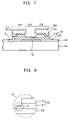
- FIG. 7 is a cross-sectional view illustrating the second metal layer corresponding to the first area and the semiconductor layer of which a portion is etched.
- the second metal layer 140 exposed by removing the photoresist film 201 of the first area 210 is etched, for example, by an etchant to form a source electrode 142 and a drain electrode 144 on the semiconductor layer 130 .
- the second metal layer 140 between the source electrode 142 and the drain electrode 144 is etched, the second semiconductor layer 134 corresponding to the first area 210 is exposed.
- the exposed second semiconductor layer 134 is etched by, for example, an etchant. In this process, a portion of the first semiconductor layer 132 may be etched. A portion ‘C’ of the remaining photoresist film 202 is lost while the second metal layer 140 and the second semiconductor layer 134 are etched.
- FIG. 8 is a partially enlarged view illustrating the portion ‘D’ illustrated in FIG. 7 .
- the first semiconductor layer 132 when a portion of the second semiconductor layer 134 and a portion of the first semiconductor layer 132 are etched, the first semiconductor layer 132 includes a protrusion ‘E’ protruding in a lateral direction. As the lost amount of the remaining photoresist film 202 is relatively small in an etching process, the protruding length of the protrusion ‘E’ the first semiconductor layer 132 is relatively small in comparison to when a positive photoresist film is used. Thus, the aperture ratio of a pixel is prevented from decreasing.
- FIG. 9 is a cross-sectional view illustrating the substrate wherein the remaining photoresist film is completely removed.
- the remaining photoresist film 202 is completely removed through an ashing process using oxygen plasma.
- the semiconductor layer 130 is hardly etched, as the etching selectivity of the semiconductor layer 130 is large with respect to the oxygen plasma.
- the TFT substrate is completely formed.
- a protecting layer may be formed on the substrate 100 to cover the source electrode 142 and the drain electrode 144 .
- a contact hole may be formed at the protecting layer corresponding to the drain electrode 144 through an exposure process and a developing process.
- a third metal layer may be formed on the protecting layer.
- the third metal layer may serve as a pixel electrode in the TFT substrate and be electrically connected to the drain electrode via the contact hole.
- the method of manufacturing a TFT substrate according to an exemplary embodiment of the present invention forms a negative photoresist film using a negative photoresist composition including a dye
- the method of manufacturing a TFT substrate may stably form a TFT substrate while also having the benefits associated with using negative photoresist films.
- a negative photoresist film formed using the photoresist composition of the exemplary embodiments of the present invention has a relatively large taper angle so that the lost amount of the negative photoresist film in an etching process is relatively small in comparison with a positive photoresist film.
- the protruding length of a semiconductor layer is reduced so that the aperture ratio of a pixel is prevented from decreasing.
- the photoresist composition of the exemplary embodiments of the present invention reduces the contrast of a negative photoresist film to stably form a halftone photoresist film. Also, a four-mask process using the photoresist composition may stably form a TFT substrate.
- a photoresist composition in accordance with exemplary embodiments of the present invention is also beneficial with respect to heat resistance and developing characteristics.
- the method of manufacturing a TFT substrate of exemplary embodiments of the present invention also increases the residual uniformity of a photoresist film between a source electrode and a drain electrode to prevent a short circuit and a pixel defect.
Landscapes
- Engineering & Computer Science (AREA)
- Physics & Mathematics (AREA)
- General Physics & Mathematics (AREA)
- Microelectronics & Electronic Packaging (AREA)
- Power Engineering (AREA)
- Condensed Matter Physics & Semiconductors (AREA)
- Computer Hardware Design (AREA)
- Spectroscopy & Molecular Physics (AREA)
- Ceramic Engineering (AREA)
- Manufacturing & Machinery (AREA)
- Architecture (AREA)
- Structural Engineering (AREA)
- Materials For Photolithography (AREA)
- Thin Film Transistor (AREA)
- Exposure And Positioning Against Photoresist Photosensitive Materials (AREA)
- Photosensitive Polymer And Photoresist Processing (AREA)
- Heterocyclic Carbon Compounds Containing A Hetero Ring Having Oxygen Or Sulfur (AREA)
Applications Claiming Priority (2)
| Application Number | Priority Date | Filing Date | Title |
|---|---|---|---|
| KR2005-77308 | 2005-08-23 | ||
| KR1020050077308A KR101298940B1 (ko) | 2005-08-23 | 2005-08-23 | 포토레지스트 조성물 및 이를 이용한 박막 트랜지스터기판의 제조방법 |
Publications (2)
| Publication Number | Publication Date |
|---|---|
| US20070048662A1 US20070048662A1 (en) | 2007-03-01 |
| US7595143B2 true US7595143B2 (en) | 2009-09-29 |
Family
ID=37804631
Family Applications (1)
| Application Number | Title | Priority Date | Filing Date |
|---|---|---|---|
| US11/508,079 Expired - Fee Related US7595143B2 (en) | 2005-08-23 | 2006-08-22 | Photoresist composition and method of manufacturing a thin-film transistor substrate using the same |
Country Status (5)
| Country | Link |
|---|---|
| US (1) | US7595143B2 (zh) |
| JP (1) | JP4964534B2 (zh) |
| KR (1) | KR101298940B1 (zh) |
| CN (1) | CN1936705B (zh) |
| TW (1) | TWI470344B (zh) |
Cited By (10)
| Publication number | Priority date | Publication date | Assignee | Title |
|---|---|---|---|---|
| US20090002591A1 (en) * | 2007-06-29 | 2009-01-01 | Semiconductor Energy Laboratory Co., Ltd. | Liquid crystal display device |
| US20090001375A1 (en) * | 2007-06-29 | 2009-01-01 | Semiconductor Energy Laboratory Co., Ltd. | Light-emitting device |
| US8624237B2 (en) | 2008-07-31 | 2014-01-07 | Semiconductor Energy Laboratory Co., Ltd. | Semiconductor device and method for manufacturing the same |
| US8842230B2 (en) | 2007-07-06 | 2014-09-23 | Semiconductor Energy Laboratory Co., Ltd. | Liquid crystal display device |
| US8980685B2 (en) | 2008-10-24 | 2015-03-17 | Semiconductor Energy Laboratory Co., Ltd. | Method for manufacturing thin film transistor using multi-tone mask |
| US9660092B2 (en) | 2011-08-31 | 2017-05-23 | Semiconductor Energy Laboratory Co., Ltd. | Oxide semiconductor thin film transistor including oxygen release layer |
| US9766542B2 (en) | 2013-07-03 | 2017-09-19 | Kempur Microelectronics, Inc. | Negative chemically-amplified photoresist and imaging method thereof |
| US10256349B2 (en) | 2008-09-01 | 2019-04-09 | Semiconductor Energy Laboratory Co., Ltd. | Semiconductor device and method for manufacturing the semiconductor device |
| US10332996B2 (en) | 2009-12-04 | 2019-06-25 | Semiconductor Energy Laboratory Co., Ltd. | Semiconductor device and manufacturing method thereof |
| US10937897B2 (en) | 2008-07-31 | 2021-03-02 | Semiconductor Energy Laboratory Co., Ltd. | Semiconductor device and method for manufacturing the same |
Families Citing this family (25)
| Publication number | Priority date | Publication date | Assignee | Title |
|---|---|---|---|---|
| JP4850582B2 (ja) * | 2006-05-24 | 2012-01-11 | 住友化学株式会社 | 着色感光性樹脂組成物、カラーフィルタ、イメージセンサおよびカメラシステム |
| KR100849190B1 (ko) * | 2007-03-19 | 2008-07-30 | 주식회사 하이닉스반도체 | 반도체 소자의 미세 패턴 형성 방법 |
| KR101385946B1 (ko) * | 2007-04-02 | 2014-04-16 | 주식회사 동진쎄미켐 | 포토레지스트 조성물 및 이를 이용한 포토레지스트 패턴의형성 방법 |
| KR101392291B1 (ko) | 2007-04-13 | 2014-05-07 | 주식회사 동진쎄미켐 | 포토레지스트 조성물 및 이를 이용한 박막트랜지스터기판의 제조방법 |
| KR20080107314A (ko) * | 2007-06-06 | 2008-12-10 | 후지필름 가부시키가이샤 | 박층 금속막 재료 및 그 제조 방법 |
| US8334537B2 (en) * | 2007-07-06 | 2012-12-18 | Semiconductor Energy Laboratory Co., Ltd. | Light-emitting device |
| US8786793B2 (en) * | 2007-07-27 | 2014-07-22 | Semiconductor Energy Laboratory Co., Ltd. | Display device and manufacturing method thereof |
| US8349671B2 (en) * | 2007-09-03 | 2013-01-08 | Semiconductor Energy Laboratory Co., Ltd. | Methods for manufacturing thin film transistor and display device |
| KR101523353B1 (ko) * | 2007-12-03 | 2015-05-27 | 가부시키가이샤 한도오따이 에네루기 켄큐쇼 | 박막트랜지스터 및 반도체 장치 |
| US8492459B2 (en) * | 2007-12-13 | 2013-07-23 | Lg Display Co., Ltd. | Ink composition and method of forming a pattern using the same |
| JP5336793B2 (ja) * | 2008-08-29 | 2013-11-06 | 富士フイルム株式会社 | パターン形成体の製造方法および電磁ビーム加工装置 |
| US9082857B2 (en) * | 2008-09-01 | 2015-07-14 | Semiconductor Energy Laboratory Co., Ltd. | Semiconductor device comprising an oxide semiconductor layer |
| EP2180518B1 (en) * | 2008-10-24 | 2018-04-25 | Semiconductor Energy Laboratory Co, Ltd. | Method for manufacturing semiconductor device |
| US8741702B2 (en) * | 2008-10-24 | 2014-06-03 | Semiconductor Energy Laboratory Co., Ltd. | Method for manufacturing semiconductor device |
| WO2010047288A1 (en) * | 2008-10-24 | 2010-04-29 | Semiconductor Energy Laboratory Co., Ltd. | Method for manufacturing semiconductordevice |
| JP5557559B2 (ja) * | 2009-03-11 | 2014-07-23 | 住友化学株式会社 | 化学増幅型ポジ型フォトレジスト組成物、該組成物に用いられる重合体、及び該重合体の構成単位を導く化合物 |
| US20110207527A1 (en) * | 2009-08-21 | 2011-08-25 | Aristocrat Technologies Australia Pty Limited | Method of gaming, a game controller and a gaming system |
| CN101907946A (zh) * | 2010-08-13 | 2010-12-08 | 牧东光电(苏州)有限公司 | 触控面板线路单边外扩的方法 |
| US8536571B2 (en) * | 2011-01-12 | 2013-09-17 | Semiconductor Energy Laboratory Co., Ltd. | Manufacturing method of semiconductor device |
| TWI421638B (zh) * | 2011-05-11 | 2014-01-01 | Chi Mei Corp | 正型感光性樹脂組成物及使用該組成物形成圖案的方法 |
| US8932945B2 (en) * | 2012-07-09 | 2015-01-13 | Taiwan Semiconductor Manufacturing Company, Ltd. | Wafer alignment system and method |
| CN103809378A (zh) * | 2014-01-26 | 2014-05-21 | 京东方科技集团股份有限公司 | 一种负性光刻胶及其制备方法、使用方法 |
| CN105742238A (zh) * | 2016-03-02 | 2016-07-06 | 京东方科技集团股份有限公司 | 孔结构和阵列基板及其制作方法、探测装置和显示装置 |
| KR102540963B1 (ko) * | 2017-12-27 | 2023-06-07 | 삼성전자주식회사 | 미세 패턴 형성 방법 및 기판 처리 장치 |
| CN108417583B (zh) * | 2018-03-09 | 2021-10-29 | 惠科股份有限公司 | 一种阵列基板的制造方法和阵列基板 |
Citations (9)
| Publication number | Priority date | Publication date | Assignee | Title |
|---|---|---|---|---|
| US5731110A (en) * | 1993-02-02 | 1998-03-24 | Sumitomo Chemical Company, Limited | Photoresist composition for use in color filters |
| US6335276B1 (en) * | 1998-11-26 | 2002-01-01 | Samsung Electronics Co., Ltd. | Method for manufacturing a thin film transistor array panel for a liquid crystal display and a photolithography method for fabricating thin films |
| US6576394B1 (en) * | 2000-06-16 | 2003-06-10 | Clariant Finance (Bvi) Limited | Negative-acting chemically amplified photoresist composition |
| US6762802B2 (en) * | 2000-05-12 | 2004-07-13 | Renesas Technology Corp. | Liquid crystal display device and fabrication method thereof |
| US6872514B2 (en) * | 2002-03-25 | 2005-03-29 | Shin-Etsu Chemical Co., Ltd. | Polymers, resist compositions and patterning process |
| US7026091B2 (en) * | 2003-07-22 | 2006-04-11 | Industrial Technology Research Institute | Positive photoresist composition and patterning process using the same |
| US7291439B2 (en) * | 2005-07-08 | 2007-11-06 | Samsung Electronics Co., Ltd. | Photoresist composition, method for forming film pattern using the same, and method for manufacturing thin film transistor array panel using the same |
| US7297452B2 (en) * | 2004-12-24 | 2007-11-20 | Samsung Electronics Co., Ltd. | Photosensitive resin composition, thin film panel made with photosensitive composition, and method for manufacturing thin film panel |
| US7338737B2 (en) * | 2004-12-16 | 2008-03-04 | Samsung Electronics Co., Ltd. | Photosensitive resin composition, thin film panel made with photosensitive resin composition, and method for manufacturing thin film panel |
Family Cites Families (9)
| Publication number | Priority date | Publication date | Assignee | Title |
|---|---|---|---|---|
| JPH0736179A (ja) * | 1993-07-19 | 1995-02-07 | Tokyo Ohka Kogyo Co Ltd | ネガ型感光性樹脂組成物 |
| JPH10228109A (ja) * | 1997-02-14 | 1998-08-25 | Fuji Photo Film Co Ltd | ネガ型画像記録材料 |
| JP2000258904A (ja) * | 1999-03-04 | 2000-09-22 | Fujifilm Olin Co Ltd | ネガ型化学増幅系感光性組成物 |
| US6678018B2 (en) * | 2000-02-10 | 2004-01-13 | Samsung Electronics Co., Ltd. | Thin film transistor array substrate for a liquid crystal display and the method for fabricating the same |
| WO2001061410A1 (fr) * | 2000-02-21 | 2001-08-23 | Zeon Corporation | Composition de resist |
| JP4370668B2 (ja) * | 2000-03-29 | 2009-11-25 | Jsr株式会社 | メッキ造形物製造用ポジ型感放射線性樹脂組成物およびメッキ造形物の製造方法 |
| JP4401033B2 (ja) * | 2001-03-19 | 2010-01-20 | Azエレクトロニックマテリアルズ株式会社 | ネガ型感光性樹脂組成物及びこれを用いた表示デバイス |
| KR100947525B1 (ko) * | 2003-03-12 | 2010-03-12 | 삼성전자주식회사 | 액정 표시 장치용 박막 트랜지스터 기판 및 이의 제조방법 |
| JP4522660B2 (ja) * | 2003-03-14 | 2010-08-11 | シャープ株式会社 | 薄膜トランジスタ基板の製造方法 |
-
2005
- 2005-08-23 KR KR1020050077308A patent/KR101298940B1/ko active IP Right Grant
-
2006
- 2006-08-22 US US11/508,079 patent/US7595143B2/en not_active Expired - Fee Related
- 2006-08-22 JP JP2006224979A patent/JP4964534B2/ja active Active
- 2006-08-23 CN CN2006101447713A patent/CN1936705B/zh not_active Expired - Fee Related
- 2006-08-23 TW TW95130994A patent/TWI470344B/zh not_active IP Right Cessation
Patent Citations (9)
| Publication number | Priority date | Publication date | Assignee | Title |
|---|---|---|---|---|
| US5731110A (en) * | 1993-02-02 | 1998-03-24 | Sumitomo Chemical Company, Limited | Photoresist composition for use in color filters |
| US6335276B1 (en) * | 1998-11-26 | 2002-01-01 | Samsung Electronics Co., Ltd. | Method for manufacturing a thin film transistor array panel for a liquid crystal display and a photolithography method for fabricating thin films |
| US6762802B2 (en) * | 2000-05-12 | 2004-07-13 | Renesas Technology Corp. | Liquid crystal display device and fabrication method thereof |
| US6576394B1 (en) * | 2000-06-16 | 2003-06-10 | Clariant Finance (Bvi) Limited | Negative-acting chemically amplified photoresist composition |
| US6872514B2 (en) * | 2002-03-25 | 2005-03-29 | Shin-Etsu Chemical Co., Ltd. | Polymers, resist compositions and patterning process |
| US7026091B2 (en) * | 2003-07-22 | 2006-04-11 | Industrial Technology Research Institute | Positive photoresist composition and patterning process using the same |
| US7338737B2 (en) * | 2004-12-16 | 2008-03-04 | Samsung Electronics Co., Ltd. | Photosensitive resin composition, thin film panel made with photosensitive resin composition, and method for manufacturing thin film panel |
| US7297452B2 (en) * | 2004-12-24 | 2007-11-20 | Samsung Electronics Co., Ltd. | Photosensitive resin composition, thin film panel made with photosensitive composition, and method for manufacturing thin film panel |
| US7291439B2 (en) * | 2005-07-08 | 2007-11-06 | Samsung Electronics Co., Ltd. | Photoresist composition, method for forming film pattern using the same, and method for manufacturing thin film transistor array panel using the same |
Cited By (27)
| Publication number | Priority date | Publication date | Assignee | Title |
|---|---|---|---|---|
| US20090002591A1 (en) * | 2007-06-29 | 2009-01-01 | Semiconductor Energy Laboratory Co., Ltd. | Liquid crystal display device |
| US20090001375A1 (en) * | 2007-06-29 | 2009-01-01 | Semiconductor Energy Laboratory Co., Ltd. | Light-emitting device |
| US8921858B2 (en) | 2007-06-29 | 2014-12-30 | Semiconductor Energy Laboratory Co., Ltd. | Light-emitting device |
| US9176353B2 (en) | 2007-06-29 | 2015-11-03 | Semiconductor Energy Laboratory Co., Ltd. | Liquid crystal display device |
| US12066730B2 (en) * | 2007-07-06 | 2024-08-20 | Semiconductor Energy Laboratory Co., Ltd. | Liquid crystal display device |
| US8842230B2 (en) | 2007-07-06 | 2014-09-23 | Semiconductor Energy Laboratory Co., Ltd. | Liquid crystal display device |
| US11726378B2 (en) | 2007-07-06 | 2023-08-15 | Semiconductor Energy Laboratory Co., Ltd. | Liquid crystal display device |
| US9188825B2 (en) | 2007-07-06 | 2015-11-17 | Semiconductor Energy Laboratory Co., Ltd. | Liquid crystal display device |
| US11194207B2 (en) | 2007-07-06 | 2021-12-07 | Semiconductor Energy Laboratory Co., Ltd. | Liquid crystal display device |
| US10338447B2 (en) | 2007-07-06 | 2019-07-02 | Semiconductor Energy Laboratory Co., Ltd. | Liquid crystal display device |
| US9766526B2 (en) | 2007-07-06 | 2017-09-19 | Semiconductor Energy Laboratory Co., Ltd. | Liquid crystal display device |
| US10712625B2 (en) | 2007-07-06 | 2020-07-14 | Semiconductor Energy Laboratory Co., Ltd. | Liquid crystal display device |
| US10678107B2 (en) | 2007-07-06 | 2020-06-09 | Semiconductor Energy Laboratory Co., Ltd. | Liquid crystal display device |
| US10937897B2 (en) | 2008-07-31 | 2021-03-02 | Semiconductor Energy Laboratory Co., Ltd. | Semiconductor device and method for manufacturing the same |
| US9496406B2 (en) | 2008-07-31 | 2016-11-15 | Semiconductor Energy Laboratory Co., Ltd. | Semiconductor device and method for manufacturing the same |
| US12074210B2 (en) | 2008-07-31 | 2024-08-27 | Semiconductor Energy Laboratory Co., Ltd. | Semiconductor device and method for manufacturing the same |
| US8624237B2 (en) | 2008-07-31 | 2014-01-07 | Semiconductor Energy Laboratory Co., Ltd. | Semiconductor device and method for manufacturing the same |
| US12068329B2 (en) | 2008-07-31 | 2024-08-20 | Semiconductor Energy Laboratory Co., Ltd. | Semiconductor device and method for manufacturing the same |
| US11296121B2 (en) | 2008-07-31 | 2022-04-05 | Semiconductor Energy Laboratory Co., Ltd. | Semiconductor device and method for manufacturing the same |
| US11201249B2 (en) | 2008-09-01 | 2021-12-14 | Semiconductor Energy Laboratory Co., Ltd. | Liquid crystal display device comprising an oxide semiconductor |
| US11824124B2 (en) | 2008-09-01 | 2023-11-21 | Semiconductor Energy Laboratory Co., Ltd. | Liquid crystal display device including transistor comprising oxide semiconductor |
| US10734530B2 (en) | 2008-09-01 | 2020-08-04 | Semiconductor Energy Laboratory Co., Ltd. | Semiconductor device comprising oxide semiconductor |
| US10256349B2 (en) | 2008-09-01 | 2019-04-09 | Semiconductor Energy Laboratory Co., Ltd. | Semiconductor device and method for manufacturing the semiconductor device |
| US8980685B2 (en) | 2008-10-24 | 2015-03-17 | Semiconductor Energy Laboratory Co., Ltd. | Method for manufacturing thin film transistor using multi-tone mask |
| US10332996B2 (en) | 2009-12-04 | 2019-06-25 | Semiconductor Energy Laboratory Co., Ltd. | Semiconductor device and manufacturing method thereof |
| US9660092B2 (en) | 2011-08-31 | 2017-05-23 | Semiconductor Energy Laboratory Co., Ltd. | Oxide semiconductor thin film transistor including oxygen release layer |
| US9766542B2 (en) | 2013-07-03 | 2017-09-19 | Kempur Microelectronics, Inc. | Negative chemically-amplified photoresist and imaging method thereof |
Also Published As
| Publication number | Publication date |
|---|---|
| KR101298940B1 (ko) | 2013-08-22 |
| KR20070023103A (ko) | 2007-02-28 |
| TW200722910A (en) | 2007-06-16 |
| JP2007058216A (ja) | 2007-03-08 |
| US20070048662A1 (en) | 2007-03-01 |
| JP4964534B2 (ja) | 2012-07-04 |
| CN1936705B (zh) | 2011-12-21 |
| TWI470344B (zh) | 2015-01-21 |
| CN1936705A (zh) | 2007-03-28 |
Similar Documents
| Publication | Publication Date | Title |
|---|---|---|
| US7595143B2 (en) | Photoresist composition and method of manufacturing a thin-film transistor substrate using the same | |
| KR101392291B1 (ko) | 포토레지스트 조성물 및 이를 이용한 박막트랜지스터기판의 제조방법 | |
| US9366959B2 (en) | Negative photosensitive resin composition and application thereof | |
| KR101348607B1 (ko) | 포토레지스트 조성물 및 이를 이용한 박막 패터닝 방법과 이를 이용한 액정 표시 패널의 제조 방법 | |
| US20110294243A1 (en) | Photoresist composition and method of forming photoresist pattern using the same | |
| KR20090109432A (ko) | 감광성 수지, 상기 감광성 수지를 사용한 패턴의 형성 방법및 표시판의 제조 방법 | |
| US20070003860A1 (en) | Substrate adhesion improver for photosensitive resin composition and photosensitive resin composition containing the same | |
| KR101430962B1 (ko) | 포토레지스트 조성물 및 이를 이용한 어레이 기판의 제조방법 | |
| KR100585301B1 (ko) | 액정소자용 화학증폭형 포지티브형 레지스트 조성물 | |
| KR101034347B1 (ko) | 감광성 수지 조성물 | |
| US8808963B2 (en) | Photoresist composition and method of manufacturing array substrate using the same | |
| KR20070066445A (ko) | 표시 기판의 제조방법 | |
| US20230037563A1 (en) | Metal containing photoresist developer composition, and method of forming patterns including developing step using the same | |
| KR20090040584A (ko) | 감광성 수지조성물 및 이에 의해 제조된 액정표시소자. | |
| KR101564403B1 (ko) | 박막 트랜지스터 표시판의 제조 방법 및 이에 사용되는 네가티브 포토레지스트 조성물 | |
| JP4446181B2 (ja) | パターン形成方法 | |
| KR101205471B1 (ko) | 액정표시소자용 감광성 수지 조성물 | |
| JP2007272002A (ja) | レジストパターン形成方法及び感光性樹脂組成物 | |
| KR20070080637A (ko) | 패턴 형성용 네거티브 포토레지스트 조성물 및 이를 이용한표시장치 패턴 형성 방법 | |
| KR20070008924A (ko) | 전계 형성 전극의 제조 방법 및 이를 이용한 액정 표시장치의 제조 방법 |
Legal Events
| Date | Code | Title | Description |
|---|---|---|---|
| AS | Assignment |
Owner name: SAMSUNG ELECTRONICS CO., LTD., KOREA, REPUBLIC OF Free format text: ASSIGNMENT OF ASSIGNORS INTEREST;ASSIGNORS:PARK, JEONG-MIN;LEE, HI-KUK;YOUN, HYOC-MIN;AND OTHERS;REEL/FRAME:018222/0494;SIGNING DATES FROM 20060802 TO 20060817 |
|
| STCF | Information on status: patent grant |
Free format text: PATENTED CASE |
|
| FEPP | Fee payment procedure |
Free format text: PAYOR NUMBER ASSIGNED (ORIGINAL EVENT CODE: ASPN); ENTITY STATUS OF PATENT OWNER: LARGE ENTITY |
|
| AS | Assignment |
Owner name: SAMSUNG DISPLAY CO., LTD., KOREA, REPUBLIC OF Free format text: ASSIGNMENT OF ASSIGNORS INTEREST;ASSIGNOR:SAMSUNG ELECTRONICS CO., LTD.;REEL/FRAME:029045/0860 Effective date: 20120904 |
|
| FEPP | Fee payment procedure |
Free format text: PAYOR NUMBER ASSIGNED (ORIGINAL EVENT CODE: ASPN); ENTITY STATUS OF PATENT OWNER: LARGE ENTITY Free format text: PAYER NUMBER DE-ASSIGNED (ORIGINAL EVENT CODE: RMPN); ENTITY STATUS OF PATENT OWNER: LARGE ENTITY |
|
| FPAY | Fee payment |
Year of fee payment: 4 |
|
| FPAY | Fee payment |
Year of fee payment: 8 |
|
| FEPP | Fee payment procedure |
Free format text: MAINTENANCE FEE REMINDER MAILED (ORIGINAL EVENT CODE: REM.); ENTITY STATUS OF PATENT OWNER: LARGE ENTITY |
|
| LAPS | Lapse for failure to pay maintenance fees |
Free format text: PATENT EXPIRED FOR FAILURE TO PAY MAINTENANCE FEES (ORIGINAL EVENT CODE: EXP.); ENTITY STATUS OF PATENT OWNER: LARGE ENTITY |
|
| STCH | Information on status: patent discontinuation |
Free format text: PATENT EXPIRED DUE TO NONPAYMENT OF MAINTENANCE FEES UNDER 37 CFR 1.362 |
|
| FP | Lapsed due to failure to pay maintenance fee |
Effective date: 20210929 |