US7510759B2 - Electronic part and manufacturing method thereof - Google Patents
Electronic part and manufacturing method thereof Download PDFInfo
- Publication number
- US7510759B2 US7510759B2 US10/541,321 US54132105A US7510759B2 US 7510759 B2 US7510759 B2 US 7510759B2 US 54132105 A US54132105 A US 54132105A US 7510759 B2 US7510759 B2 US 7510759B2
- Authority
- US
- United States
- Prior art keywords
- substrate
- conductive pattern
- oxide layer
- metal oxide
- electronic component
- Prior art date
- Legal status (The legal status is an assumption and is not a legal conclusion. Google has not performed a legal analysis and makes no representation as to the accuracy of the status listed.)
- Expired - Fee Related, expires
Links
Images


Classifications
-
- H—ELECTRICITY
- H05—ELECTRIC TECHNIQUES NOT OTHERWISE PROVIDED FOR
- H05K—PRINTED CIRCUITS; CASINGS OR CONSTRUCTIONAL DETAILS OF ELECTRIC APPARATUS; MANUFACTURE OF ASSEMBLAGES OF ELECTRICAL COMPONENTS
- H05K3/00—Apparatus or processes for manufacturing printed circuits
- H05K3/22—Secondary treatment of printed circuits
- H05K3/24—Reinforcing the conductive pattern
- H05K3/245—Reinforcing conductive patterns made by printing techniques or by other techniques for applying conductive pastes, inks or powders; Reinforcing other conductive patterns by such techniques
- H05K3/246—Reinforcing conductive paste, ink or powder patterns by other methods, e.g. by plating
-
- H—ELECTRICITY
- H05—ELECTRIC TECHNIQUES NOT OTHERWISE PROVIDED FOR
- H05K—PRINTED CIRCUITS; CASINGS OR CONSTRUCTIONAL DETAILS OF ELECTRIC APPARATUS; MANUFACTURE OF ASSEMBLAGES OF ELECTRICAL COMPONENTS
- H05K3/00—Apparatus or processes for manufacturing printed circuits
- H05K3/22—Secondary treatment of printed circuits
- H05K3/24—Reinforcing the conductive pattern
-
- H—ELECTRICITY
- H05—ELECTRIC TECHNIQUES NOT OTHERWISE PROVIDED FOR
- H05K—PRINTED CIRCUITS; CASINGS OR CONSTRUCTIONAL DETAILS OF ELECTRIC APPARATUS; MANUFACTURE OF ASSEMBLAGES OF ELECTRICAL COMPONENTS
- H05K3/00—Apparatus or processes for manufacturing printed circuits
- H05K3/22—Secondary treatment of printed circuits
- H05K3/28—Applying non-metallic protective coatings
-
- H—ELECTRICITY
- H05—ELECTRIC TECHNIQUES NOT OTHERWISE PROVIDED FOR
- H05K—PRINTED CIRCUITS; CASINGS OR CONSTRUCTIONAL DETAILS OF ELECTRIC APPARATUS; MANUFACTURE OF ASSEMBLAGES OF ELECTRICAL COMPONENTS
- H05K1/00—Printed circuits
- H05K1/02—Details
- H05K1/09—Use of materials for the conductive, e.g. metallic pattern
- H05K1/092—Dispersed materials, e.g. conductive pastes or inks
-
- H—ELECTRICITY
- H05—ELECTRIC TECHNIQUES NOT OTHERWISE PROVIDED FOR
- H05K—PRINTED CIRCUITS; CASINGS OR CONSTRUCTIONAL DETAILS OF ELECTRIC APPARATUS; MANUFACTURE OF ASSEMBLAGES OF ELECTRICAL COMPONENTS
- H05K1/00—Printed circuits
- H05K1/16—Printed circuits incorporating printed electric components, e.g. printed resistor, capacitor, inductor
- H05K1/165—Printed circuits incorporating printed electric components, e.g. printed resistor, capacitor, inductor incorporating printed inductors
-
- H—ELECTRICITY
- H05—ELECTRIC TECHNIQUES NOT OTHERWISE PROVIDED FOR
- H05K—PRINTED CIRCUITS; CASINGS OR CONSTRUCTIONAL DETAILS OF ELECTRIC APPARATUS; MANUFACTURE OF ASSEMBLAGES OF ELECTRICAL COMPONENTS
- H05K2201/00—Indexing scheme relating to printed circuits covered by H05K1/00
- H05K2201/03—Conductive materials
- H05K2201/0332—Structure of the conductor
- H05K2201/0335—Layered conductors or foils
- H05K2201/0347—Overplating, e.g. for reinforcing conductors or bumps; Plating over filled vias
-
- H—ELECTRICITY
- H05—ELECTRIC TECHNIQUES NOT OTHERWISE PROVIDED FOR
- H05K—PRINTED CIRCUITS; CASINGS OR CONSTRUCTIONAL DETAILS OF ELECTRIC APPARATUS; MANUFACTURE OF ASSEMBLAGES OF ELECTRICAL COMPONENTS
- H05K2203/00—Indexing scheme relating to apparatus or processes for manufacturing printed circuits covered by H05K3/00
- H05K2203/03—Metal processing
- H05K2203/0315—Oxidising metal
-
- Y—GENERAL TAGGING OF NEW TECHNOLOGICAL DEVELOPMENTS; GENERAL TAGGING OF CROSS-SECTIONAL TECHNOLOGIES SPANNING OVER SEVERAL SECTIONS OF THE IPC; TECHNICAL SUBJECTS COVERED BY FORMER USPC CROSS-REFERENCE ART COLLECTIONS [XRACs] AND DIGESTS
- Y10—TECHNICAL SUBJECTS COVERED BY FORMER USPC
- Y10T—TECHNICAL SUBJECTS COVERED BY FORMER US CLASSIFICATION
- Y10T428/00—Stock material or miscellaneous articles
- Y10T428/24—Structurally defined web or sheet [e.g., overall dimension, etc.]
- Y10T428/24802—Discontinuous or differential coating, impregnation or bond [e.g., artwork, printing, retouched photograph, etc.]
- Y10T428/24917—Discontinuous or differential coating, impregnation or bond [e.g., artwork, printing, retouched photograph, etc.] including metal layer
-
- Y—GENERAL TAGGING OF NEW TECHNOLOGICAL DEVELOPMENTS; GENERAL TAGGING OF CROSS-SECTIONAL TECHNOLOGIES SPANNING OVER SEVERAL SECTIONS OF THE IPC; TECHNICAL SUBJECTS COVERED BY FORMER USPC CROSS-REFERENCE ART COLLECTIONS [XRACs] AND DIGESTS
- Y10—TECHNICAL SUBJECTS COVERED BY FORMER USPC
- Y10T—TECHNICAL SUBJECTS COVERED BY FORMER US CLASSIFICATION
- Y10T428/00—Stock material or miscellaneous articles
- Y10T428/24—Structurally defined web or sheet [e.g., overall dimension, etc.]
- Y10T428/24802—Discontinuous or differential coating, impregnation or bond [e.g., artwork, printing, retouched photograph, etc.]
- Y10T428/24926—Discontinuous or differential coating, impregnation or bond [e.g., artwork, printing, retouched photograph, etc.] including ceramic, glass, porcelain or quartz layer
Definitions
- the present invention relates to electronic components to be used in a variety of electronic devices and communication devices, and a method of manufacturing the same electronic components.
- FIG. 9 shows a sectional view of the pattern.
- conductive pattern 22 is formed on substrate 21 by printing.
- insulating protective film 23 made of glass.
- This film is formed by printing glass-paste, i.e. a mixture of glass powder as a major component, binder and solvent, at a given thickness, then the paste is dried and baked to be the film.
- Use of compound organic material such as glass-epoxy as substrate 21 employs insulating protective film 23 made of organic material because it is difficult for this substrate 21 to undergo a heat treatment at an excessively high temperature.
- film 23 is formed by screen-printing resin paste made mainly of organic material, then the resin undergoes a heat curing process to be film 23 .
- the sputtering method one of thin-film methods can be used for forming SiO 2 film as insulating protective film 23 .
- Fine conductive patterns made from electrode material such as Ag is formed on substrate 21 made of the foregoing materials, then insulating protective film 23 is formed by a printing method such as screen-printing. Film 23 thus formed tends to be short of uniformity of film thickness, or tends to produce air bubbles 24 and air gaps 25 . As a result, conductive pattern 22 decreases its reliability. Although the foregoing printing method is good at productivity, it is poor at forming film 23 uniform in thickness with accuracy because of viscoelasticity characteristics of the paste.
- film 23 becomes thinner or tends to trap air-bubbles 24 in patterns 22 .
- a narrow space between patterns 22 tends to produce air-gaps 25 because the spaces cannot be fully filled with paste.
- the thin-film method can form a film uniformly in thickness on a plane section of pattern 22 (parallel with the surface of substrate 21 ), so that no problem is found. However, it is difficult for the thin-film method to form a film uniformly in thickness on pattern's wall face (vertical with respect to the surface of substrate 21 ).
- insulating protective film 23 is formed by the conventional method, it is difficult to prevent the electrode made of Ag from migrating into others.
- a higher aspect ratio (a ratio of height vs. width) of pattern 22 increases probability of incurring various defects of film 23 . As a result, it is difficult to maintain the reliability of withstanding migration.
- the present invention aims to solve the problems discussed above, and provide highly reliable electronic components having conductive patterns with a high aspect ratio.
- the present invention provides an electronic component comprising the following elements:
- the present invention provides a method of manufacturing the electronic component, the method comprising the steps of:
- FIG. 1 shows a perspective view of a common-mode choke coil as an electronic component in accordance with a first exemplary embodiment of the present invention.
- FIG. 2 shows a sectional view of the common-mode choke coil in accordance with the first embodiment shown in FIG. 1 taken along line A-A′.
- FIG. 3 shows a perspective view of a common-mode choke coil as another example in accordance with the first embodiment of the present invention.
- FIG. 4 shows a sectional view of the common-mode choke coil shown in FIG. 3 taken along line B-B′.
- FIG. 5 shows a perspective view of a common-mode choke coil as still another example in accordance with the first embodiment of the present invention.
- FIG. 6 shows a sectional view of the common-mode choke coil shown in FIG. 5 taken along line C-C′.
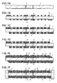
- FIG. 7A shows a sectional view illustrating a step of manufacturing the electronic component in accordance with the first exemplary embodiment of the present invention.
- FIG. 7B shows a sectional view illustrating a step of manufacturing the electronic component in accordance with the first exemplary embodiment of the present invention.
- FIG. 7C shows a sectional view illustrating a step of manufacturing the electronic component in accordance with the first exemplary embodiment of the present invention.
- FIG. 7D shows a sectional view illustrating a step of manufacturing the electronic component in accordance with the first exemplary embodiment of the present invention.
- FIG. 7E shows a sectional view illustrating a step of manufacturing the electronic component in accordance with the first exemplary embodiment of the present invention.
- FIG. 7F shows a sectional view illustrating a step of manufacturing the electronic component in accordance with the first exemplary embodiment of the present invention.
- FIG. 8 shows a sectional view illustrating an electronic component in accordance with a second exemplary embodiment of the present invention.
- FIG. 9 shows a sectional view of a conventional electronic component.
- the present invention provides an electronic component comprising the following elements:
- the electronic component of the present invention comprises the following elements:
- the electronic component of the present invention comprises the following elements:
- a ceramic substrate having a high heat resistance and being excellent in heat conductivity allows the present invention to achieve electronic components having conductive patterns fine enough for power-source modules, which outputs a high power and needs high heat resistance as well as high heat dissipation.
- electrode material which contains at least Ag
- Use of electrode material, which contains at least Ag, in the conductive patterns allows the present invention to achieve reliable electronic components having fine conductive patterns which have less loss because of low wiring resistance.
- Electrode material from the group consisting of Ag, Ag—Pt, and Ag—Pd allows the present invention to achieve electronic components of stronger anti-migration property.
- An electronic component of the present invention includes a metal oxide layer containing one of NiO, ZnO, and CuO. This structure can be achieved with ease by oxidizing a metal film formed by a plating method, so that electronic components having fine conductive patterns excellent in productivity can be obtained.
- the present invention allows obtaining a metal oxide layer having a film uniform thickness ranging from 0.5-5 ⁇ m, so that electronic components having fine conductive patterns excellent in reliability are obtainable.
- a part of the conductive patterns is exposed from the surface of the component, so that the present invention can achieve an electronic component mountable to semiconductors or other components by soldering.
- a part of the conductive patterns and a part of the substrate are exposed, so that the present invention can achieve an electronic component, on which other conductive patterns or other components can be formed.
- the present invention provides a method of manufacturing electronic components, and the method comprises the steps of:
- the present invention provides another method of manufacturing electronic components, and the method comprises the steps of:
- the present invention provides a method of manufacturing electronic components, and the method comprises the steps of:
- the present invention provides a method of manufacturing electronic components, and the method uses electroless plating as the plating method, so that a thin and uniform metal oxide layer can be formed on electronic components having complicated conductive patterns.
- the present invention provides a method of manufacturing electronic components, and the method uses a heat treatment as the oxidizing process, which is thus carried out with ease because the heat treatment is very simple.
- the manufacturing method of the present invention carries out the heat treatment at a temperature not higher than a melting point of the conductive patterns, so that the electronic components by this method have less deterioration in the patterns and fewer changes in wiring resistance.
- the present invention provides a method of manufacturing electronic components, and the method comprises the steps of:
- substrate 1 made of ceramic excellent in heat conductivity such as aluminum oxide has conductive patterns 2 on its both sides.
- Patterns 2 are made of electrode material such as Ag, and formed in a dual and helical coil-pattern.
- metal film 5 (detailed later) made of Ni or the like is formed by a plating method, then metal film 5 undergoes a heat treatment or a chemical treatment to be oxidized, so that metal oxide layer 3 is formed.
- Through-holes 4 are provided when necessary for coupling conductive patterns 2 on both the sides electrically to each other.
- metal film 5 Use of electroplating from among various plating methods for forming metal film 5 allows forming film 5 on the surface alone of conductive pattern 2 without using resist-mask.
- substrate 1 is dipped into electroplating solution for Ni (Watt solution) to undergo electrolysis, so that film 5 of Ni can be formed on the surface alone of conductive pattern 2 .
- the structure demonstrated in this embodiment allows metal oxide layer 3 to cover the entire surface of conductive pattern 2 , made of electrode material such as Ag, solidly and uniformly.
- the structure can advantageously prevent migration of Ag or insulation defectives even a conductive pattern has a high aspect ratio. Since metal film 5 of Ni or the like is formed by a plating method on the surface of pattern 2 , metal oxide layer 3 can be formed uniformly on any shape of pattern 2 . At the same time, the edge sections of pattern 2 can be covered by layer 3 in the same thickness as that of the flat section.
- metal film 5 formed uniformly by a plating method undergoes a heat treatment or a chemical treatment to be oxidized, so that metal oxide layer 3 is formed.
- a uniform and solid insulating protective film can be thus formed on the surface of a conductive resistor.
- Conductive patterns 2 are made mainly of Ag having small conductive resistance.
- substrate 1 such as an aluminum oxide substrate good at heat conduction
- the components are useful to power-supply modules that need good heat dissipation.
- Substrate 1 made of glass ceramic allows achieving a multi-layer wiring structure having built-in wiring material of Ag at an inner layer. This structure is useful to compact modules to be used at high frequencies and in portable devices that need a downsized body.
- Electrode material containing Ag among others in conductive pattern 2 allows electronic components of the present invention to exhibit their advantage to the full extent.
- Use of Ag, Ag—Pt, or Ag—Pd in conductive pattern 2 allows the electronic components of the present invention to have a lower conductive resistance value and to be more reliable. In other words, it is crucial to select a metal that does not produce non-conductive film on its surface even the heat treatment is carried out in the atmosphere.
- Metal oxide layer 3 that achieves the high reliability can be made from any material as far as metal film 5 becomes metal oxide layer 3 by heat treatment in the atmosphere. It is preferable to use at least one of NiO, ZnO, and CuO. The reason is this: The electroless plating method can be used for forming metal film 5 made of Ni, or Cu, and the electroplating method can be used for forming metal film made of Ni, Zn or Cu. Metal oxide layer 3 can be a single layer or multi-layer of film 5 .
- Metal oxide layer 3 preferably has a thickness ranging from 0.5-5 ⁇ m. A thickness less than 0.5 ⁇ m fails to obtain sufficient reliability, and a thickness greater than 5 ⁇ m fails to make fine intervals between electrodes of conductive patterns 2 .
- conductive patterns 2 are formed on both the sides of substrate 1 ; however, pattern 2 can be formed on a single side thereof with the same advantage.
- FIGS. 3 and 4 a glass ceramic substrate made of mixture of aluminum oxide powder and glass powder is used as substrate 1 .
- This coil differs from that shown in FIGS. 1 and 2 in structure, i.e. metal oxide layer 3 is formed not only on the surface of conductive pattern 2 but also on the spaces between electrodes of pattern 2 on the substrate.
- This structure allows an electronic component to form conductive pattern 2 having narrower intervals between electrodes with reliability. Since this electronic component uses a glass ceramic substrate, made by baking at a low temperature, excellent in dielectric characteristics and productivity, multi-layers can be formed in the component with ease. This component is useful for compact module components to be used at high frequencies.
- Still another coil component is demonstrated with reference to FIGS. 5 and 6 .
- this coil differs from that shown in FIGS. 1 and 2 in a structure, i.e. metal oxide layer 3 is formed on the entire surface, where conductive pattern 2 is formed, of substrate 1 .
- This structure allows metal oxide layer 3 to cover and protect conductive patterns 2 made of Ag or the like and formed not only at a given place with fine intervals between electrodes but also the other patterns 2 on the entire substrate 1 .
- the component is useful for electrical equipment of car-use requiring environment-friendly components. For instance, a compound component formed of L and C, where no fine conductive pattern 2 is needed, can employ another electrode material having a high conductive resistance. Even in such a case, i.e. electrode materials different from what is discussed previously are used, providing metal oxide layer 3 on the entire surface of substrate 1 allows achieving reliable electronic component including compound components.
- FIG. 7A A method of manufacturing the electronic component of the present invention is demonstrated hereinafter with reference to FIG. 7A-FIG . 7 F.
- substrate 1 made of aluminum oxide at a purity of 96% as an example of ceramic substrate.
- a glass-ceramic substrate made by low temperature firing and excellent in productivity can be used instead of the aluminum-oxide substrate.
- Pattern 2 is formed by printing Ag paste by an intaglio printing method, then pattern 2 is baked at 900° C. Pattern 2 can be formed by the thin-film method or the plating method instead of the method discussed above.
- Ni-film in 2 ⁇ m thickness as metal film 5 on the surfaces of conductive pattern 2 and substrate 1 by the electroless plating method using plating solution of Ni—P or Ni—B.
- metal film 5 in a given pattern is needed, use a resist material and a photo-lithograph method, thereby forming patterned metal film 5 with ease.
- metal film 5 undergoes a heat treatment in the air under the following thermal oxidation conditions: rate of temperature rise: 200° C./hour, oxidizing temperature: 900° C., and holding time: 4 hours.
- Metal oxide layer 3 including NiO is thus formed. This oxidizing treatment makes the thickness of layer 3 approx. 3.2 ⁇ m.
- metal film 5 formed of Ni preferably undergoes the thermal oxidation at not lower than 850° C. and not higher than a melting point of the electrode material of conductive pattern 2 .
- a temperature lower than 850° C. will need a longer time for the thermal oxidation, and a temperature higher than the melting point will deteriorate conductive pattern 2 or makes it difficult to maintain the pattern shape.
- end-face electrodes 7 can be made of any conductive material and preferably formed of plural layers instead of a single layer.
- metal oxide layer 3 formed by oxidizing metal film 5 is not necessarily to cover the entire surface of substrate 1 , namely, coverage on the surface of conductive pattern alone allows layer 3 to work as an insulating film to protect Ag that forms pattern 2 .
- coverage by layer 3 on the surface of pattern 2 and the spaces between electrodes on substrate 1 allows layer 3 to work as an insulating protective film with higher reliability at the following places: where closer pattern 2 is needed or between electrodes where a higher voltage is applied.
- substrate 1 is formed of organic substrate made from, e.g. glass epoxy. Use of the organic substrate allows enlarging the area of substrate 1 , thereby increasing the productivity.
- conductive pattern 2 of which surface layer includes Ag has been formed in advance by the photolithography method on the organic substrate, and Ni-plated layer having 1 ⁇ m thickness is formed on that surface layer by the electroless plating method, so that a metal film is obtained.
- the metal film undergoes an oxidation treatment.
- Use of an organic substrate is regulated by an upper limit of a heating temperature, so that the oxidation treatment is preferably carried out in the following way: Prepare acid solution of not higher than pH3, and dip substrate 1 into the solution, or place substrate 1 together with the solution in an airtight space for oxidizing substrate 1 .
- Such a chemical treatment oxidizes Ni to NiO.
- Metal oxide layer 3 thus obtained is thin and has a uniform distribution of film thickness, so that it can be formed uniformly at minute sections of conductive pattern 2 .
- Terminal electrode sections 10 are provided on the surface of substrate 1 , and these terminal electrode sections 10 are parts of conductive pattern 2 and that parts are not covered by metal oxide layer 3 , so that terminal electrode sections 10 are exposed. Presence of such terminal electrode sections 10 allows soldering terminal electrodes 11 of component 9 to electrode sections 10 with ease.
- Component 9 shown in FIG. 8 includes a semiconductor device, coil, capacitor, or resistor having terminal electrodes 11 . This structure is useful for building module components working at high frequencies.
- metal oxide layer 3 works as a pattern mask for mounting the component by soldering, so that each one of terminal electrode sections 10 can be used with ease as a mounting land. As a result, no resist is needed.
- electrical resistance pattern 8 can be formed on substrate 1 by using a thick-film or a thin-film technique. If metal oxide layer 3 exists beneath resistance pattern 8 , layer 3 and the resistance material of pattern 8 react chemically or thermally with each other, which can adversely affect a resistance value, a temperature coefficient or resistance noises. In the case of using carbon resistor as resistance pattern 8 , a surface roughness or a material of the substrate sometimes affects the resistance characteristics.
- the structure according to the present invention allows obtaining electronic components in which stable elements can be placed on substrate 1 .
- the electronic components of the present invention use a metal oxide layer as an insulating protective film, which is formed uniformly by a plating method on an insulating layer, so that a uniform and solid insulating film is obtainable with ease even the conductive pattern is minutely formed and has a high aspect ratio.
- Use of electrode material containing Ag in the conductive pattern advantageously allows obtaining the compact, accurate and reliable electronic components that have few migrations.
- the electronic components of the present invention in which a uniform and solid insulating protective film can be formed efficiently, can be widely used as reliable and compact electronic components in portable electronic devices.
Applications Claiming Priority (3)
| Application Number | Priority Date | Filing Date | Title |
|---|---|---|---|
| JP2003-402606 | 2003-12-02 | ||
| JP2003402606A JP4556422B2 (ja) | 2003-12-02 | 2003-12-02 | 電子部品およびその製造方法 |
| PCT/JP2004/017678 WO2005055683A1 (fr) | 2003-12-02 | 2004-11-29 | Piece electronique et son procede de fabrication |
Publications (2)
| Publication Number | Publication Date |
|---|---|
| US20060118905A1 US20060118905A1 (en) | 2006-06-08 |
| US7510759B2 true US7510759B2 (en) | 2009-03-31 |
Family
ID=34650037
Family Applications (1)
| Application Number | Title | Priority Date | Filing Date |
|---|---|---|---|
| US10/541,321 Expired - Fee Related US7510759B2 (en) | 2003-12-02 | 2004-11-29 | Electronic part and manufacturing method thereof |
Country Status (5)
| Country | Link |
|---|---|
| US (1) | US7510759B2 (fr) |
| EP (1) | EP1581032A4 (fr) |
| JP (1) | JP4556422B2 (fr) |
| CN (1) | CN100473258C (fr) |
| WO (1) | WO2005055683A1 (fr) |
Cited By (1)
| Publication number | Priority date | Publication date | Assignee | Title |
|---|---|---|---|---|
| US20100226109A1 (en) * | 2005-07-06 | 2010-09-09 | Seiko Epson Corporation | Electronic substrate, manufacturing method for electronic substrate, and electronic device |
Families Citing this family (21)
| Publication number | Priority date | Publication date | Assignee | Title |
|---|---|---|---|---|
| JP4652179B2 (ja) * | 2005-09-05 | 2011-03-16 | 日東電工株式会社 | 配線回路基板 |
| JP4790447B2 (ja) * | 2006-03-02 | 2011-10-12 | 日東電工株式会社 | 回路付サスペンション基板 |
| KR100764386B1 (ko) | 2006-03-20 | 2007-10-08 | 삼성전기주식회사 | 고온공정에 적합한 절연구조체 및 그 제조방법 |
| JP4749221B2 (ja) * | 2006-05-01 | 2011-08-17 | 日東電工株式会社 | 配線回路基板 |
| US9615463B2 (en) | 2006-09-22 | 2017-04-04 | Oscar Khaselev | Method for producing a high-aspect ratio conductive pattern on a substrate |
| WO2009020464A1 (fr) * | 2007-08-03 | 2009-02-12 | Fry's Metals, Inc. | Motifs conducteurs et procédés d'utilisation associés |
| US20090077093A1 (en) * | 2007-09-19 | 2009-03-19 | Joydeep Sen Sarma | Feature Discretization and Cardinality Reduction Using Collaborative Filtering Techniques |
| WO2010061563A1 (fr) * | 2008-11-27 | 2010-06-03 | 三井・デュポンポリケミカル株式会社 | Film protecteur pour composant électronique, procédé de fabrication associé, et utilisation de ce film protecteur |
| JP5482152B2 (ja) * | 2009-11-27 | 2014-04-23 | トヨタ自動車株式会社 | トランス素子とその製造方法 |
| JP6069893B2 (ja) * | 2012-06-04 | 2017-02-01 | 株式会社ジェイテクト | 電子回路装置 |
| US9113583B2 (en) * | 2012-07-31 | 2015-08-18 | General Electric Company | Electronic circuit board, assembly and a related method thereof |
| JP6311200B2 (ja) * | 2014-06-26 | 2018-04-18 | 住友電工プリントサーキット株式会社 | プリント配線板、電子部品及びプリント配線板の製造方法 |
| KR101823194B1 (ko) | 2014-10-16 | 2018-01-29 | 삼성전기주식회사 | 칩 전자부품 및 그 제조방법 |
| CN105225845B (zh) * | 2015-10-20 | 2018-01-23 | 国家纳米科学中心 | 一种超级电容器电极材料及其制备方法 |
| JP6569545B2 (ja) * | 2016-01-27 | 2019-09-04 | 住友金属鉱山株式会社 | 厚膜銅電極または配線とその形成方法 |
| US11521785B2 (en) | 2016-11-18 | 2022-12-06 | Hutchinson Technology Incorporated | High density coil design and process |
| US11387033B2 (en) * | 2016-11-18 | 2022-07-12 | Hutchinson Technology Incorporated | High-aspect ratio electroplated structures and anisotropic electroplating processes |
| JP7323268B2 (ja) * | 2018-03-16 | 2023-08-08 | 日東電工株式会社 | 磁性配線回路基板およびその製造方法 |
| EP3860317A4 (fr) * | 2018-09-27 | 2021-11-17 | Denka Company Limited | Substrat lié, circuit imprimé métallique et circuit imprimé |
| CN111370210B (zh) * | 2020-04-27 | 2021-12-10 | 安捷利(番禺)电子实业有限公司 | 一种充电线圈及无线充电终端 |
| JPWO2023281838A1 (fr) * | 2021-07-05 | 2023-01-12 |
Citations (11)
| Publication number | Priority date | Publication date | Assignee | Title |
|---|---|---|---|---|
| JPS5486766A (en) | 1977-12-22 | 1979-07-10 | Tokyo Shibaura Electric Co | Ic substrate |
| US4609611A (en) * | 1983-11-07 | 1986-09-02 | Fuji Photo Film Co., Ltd. | Light information recording medium |
| US4795670A (en) * | 1986-05-14 | 1989-01-03 | Narumi China Corporation | Multilayer ceramic substrate with circuit patterns |
| JPH08181423A (ja) | 1994-12-27 | 1996-07-12 | Nippon Telegr & Teleph Corp <Ntt> | はんだバンプ実装用端子電極構造 |
| US5665459A (en) * | 1995-03-06 | 1997-09-09 | Sumitomo Metal Ceramics Inc. | Low-temperature fired ceramic circuit substrate and thick-film paste for use in fabrication thereof |
| US5924623A (en) * | 1997-06-30 | 1999-07-20 | Honeywell Inc. | Diffusion patterned C4 bump pads |
| JP2000031625A (ja) | 1998-07-08 | 2000-01-28 | Nec Corp | はんだレジストを備えた高周波回路プリント基板 |
| JP2000174423A (ja) | 1998-12-09 | 2000-06-23 | Denso Corp | 配線基板およびその製造方法 |
| US6586683B2 (en) * | 2001-04-27 | 2003-07-01 | International Business Machines Corporation | Printed circuit board with mixed metallurgy pads and method of fabrication |
| US6717266B1 (en) * | 2002-06-18 | 2004-04-06 | Advanced Micro Devices, Inc. | Use of an alloying element to form a stable oxide layer on the surface of metal features |
| US6756306B2 (en) * | 2002-07-31 | 2004-06-29 | Advanced Micro Devices, Inc. | Low temperature dielectric deposition to improve copper electromigration performance |
Family Cites Families (8)
| Publication number | Priority date | Publication date | Assignee | Title |
|---|---|---|---|---|
| US3745045A (en) * | 1971-01-06 | 1973-07-10 | R Brenneman | Electrical contact surface using an ink containing a plating catalyst |
| US3916056A (en) * | 1972-12-29 | 1975-10-28 | Rca Corp | Photomask bearing a pattern of metal plated areas |
| JPS5145276A (en) * | 1974-10-17 | 1976-04-17 | Taiyo Yuden Kk | Denkikairobuhinno seizohoho |
| JPS5821839B2 (ja) * | 1979-05-18 | 1983-05-04 | 富士通株式会社 | プリント板 |
| DE3028044C1 (de) * | 1980-07-24 | 1981-10-08 | Vdo Adolf Schindling Ag, 6000 Frankfurt | Lötfähiges Schichtensystem |
| GB8602331D0 (en) * | 1986-01-30 | 1986-03-05 | Ici Plc | Multilayer systems |
| JP3508789B2 (ja) * | 1994-07-04 | 2004-03-22 | セイコーエプソン株式会社 | 基板の表面処理方法 |
| US5650595A (en) * | 1995-05-25 | 1997-07-22 | International Business Machines Corporation | Electronic module with multiple solder dams in soldermask window |
-
2003
- 2003-12-02 JP JP2003402606A patent/JP4556422B2/ja not_active Expired - Fee Related
-
2004
- 2004-11-29 CN CN200480001629.2A patent/CN100473258C/zh not_active Expired - Fee Related
- 2004-11-29 EP EP04819794A patent/EP1581032A4/fr not_active Withdrawn
- 2004-11-29 US US10/541,321 patent/US7510759B2/en not_active Expired - Fee Related
- 2004-11-29 WO PCT/JP2004/017678 patent/WO2005055683A1/fr not_active Application Discontinuation
Patent Citations (11)
| Publication number | Priority date | Publication date | Assignee | Title |
|---|---|---|---|---|
| JPS5486766A (en) | 1977-12-22 | 1979-07-10 | Tokyo Shibaura Electric Co | Ic substrate |
| US4609611A (en) * | 1983-11-07 | 1986-09-02 | Fuji Photo Film Co., Ltd. | Light information recording medium |
| US4795670A (en) * | 1986-05-14 | 1989-01-03 | Narumi China Corporation | Multilayer ceramic substrate with circuit patterns |
| JPH08181423A (ja) | 1994-12-27 | 1996-07-12 | Nippon Telegr & Teleph Corp <Ntt> | はんだバンプ実装用端子電極構造 |
| US5665459A (en) * | 1995-03-06 | 1997-09-09 | Sumitomo Metal Ceramics Inc. | Low-temperature fired ceramic circuit substrate and thick-film paste for use in fabrication thereof |
| US5924623A (en) * | 1997-06-30 | 1999-07-20 | Honeywell Inc. | Diffusion patterned C4 bump pads |
| JP2000031625A (ja) | 1998-07-08 | 2000-01-28 | Nec Corp | はんだレジストを備えた高周波回路プリント基板 |
| JP2000174423A (ja) | 1998-12-09 | 2000-06-23 | Denso Corp | 配線基板およびその製造方法 |
| US6586683B2 (en) * | 2001-04-27 | 2003-07-01 | International Business Machines Corporation | Printed circuit board with mixed metallurgy pads and method of fabrication |
| US6717266B1 (en) * | 2002-06-18 | 2004-04-06 | Advanced Micro Devices, Inc. | Use of an alloying element to form a stable oxide layer on the surface of metal features |
| US6756306B2 (en) * | 2002-07-31 | 2004-06-29 | Advanced Micro Devices, Inc. | Low temperature dielectric deposition to improve copper electromigration performance |
Cited By (3)
| Publication number | Priority date | Publication date | Assignee | Title |
|---|---|---|---|---|
| US20100226109A1 (en) * | 2005-07-06 | 2010-09-09 | Seiko Epson Corporation | Electronic substrate, manufacturing method for electronic substrate, and electronic device |
| US8284566B2 (en) * | 2005-07-06 | 2012-10-09 | Seiko Epson Corporation | Electronic substrate |
| US9496202B2 (en) | 2005-07-06 | 2016-11-15 | Seiko Epson Corporation | Electronic substrate |
Also Published As
| Publication number | Publication date |
|---|---|
| JP4556422B2 (ja) | 2010-10-06 |
| US20060118905A1 (en) | 2006-06-08 |
| WO2005055683A1 (fr) | 2005-06-16 |
| EP1581032A4 (fr) | 2009-10-21 |
| EP1581032A1 (fr) | 2005-09-28 |
| CN1717964A (zh) | 2006-01-04 |
| CN100473258C (zh) | 2009-03-25 |
| JP2005166873A (ja) | 2005-06-23 |
Similar Documents
| Publication | Publication Date | Title |
|---|---|---|
| US7510759B2 (en) | Electronic part and manufacturing method thereof | |
| Barlow III et al. | Ceramic interconnect technology handbook | |
| US8232479B2 (en) | Electronic apparatus | |
| JP2008085280A (ja) | 表面実装型電子部品とその製造方法 | |
| JP2007281400A (ja) | 表面実装型セラミック電子部品 | |
| JPS5852900A (ja) | セラミツク多層配線板の製造方法 | |
| JP2004140285A (ja) | 基板内蔵用チップ形抵抗器 | |
| JP3472523B2 (ja) | 電気素子内蔵配線基板 | |
| JPH06169173A (ja) | 窒化アルミニウム質基板の製造方法 | |
| JP4540223B2 (ja) | 電子部品搭載基板 | |
| KR100715152B1 (ko) | 금속 지지 기판 상에 금속 콘택 패드를 형성시키는 방법 | |
| JPH11345734A (ja) | 積層セラミックコンデンサ | |
| JP3214960B2 (ja) | 配線基板 | |
| JP2003297636A (ja) | コイル部品 | |
| Elshabini et al. | Overview of Ceramic Interconnect Technolgy | |
| JP2003318065A (ja) | 積層電子部品およびその製造方法 | |
| EP0417749A2 (fr) | Substrat pour circuit comportant des résistances intégrées à couches épaisses et son procédé de fabrication | |
| JP2006269829A (ja) | セラミック電子部品 | |
| JP2537893B2 (ja) | 電子回路基板の製造方法 | |
| JP2003078103A (ja) | 回路基板 | |
| KR100709913B1 (ko) | 적층형 칩 배리스터, 이의 제조방법 및 적층형 소자 | |
| JP2866512B2 (ja) | 配線基板 | |
| JPS6231190A (ja) | 電子回路基板及びその製造方法 | |
| JPH1098244A (ja) | 厚膜回路基板及びその製造方法 | |
| JP2738603B2 (ja) | 回路基板 |
Legal Events
| Date | Code | Title | Description |
|---|---|---|---|
| AS | Assignment |
Owner name: MATSUSHITA ELECTRIC INDUSTRIAL CO., LTD., JAPAN Free format text: ASSIGNMENT OF ASSIGNORS INTEREST;ASSIGNORS:HIMORI, TSUYOSHI;HIRAI, SHOGO;REEL/FRAME:017427/0548 Effective date: 20050516 |
|
| AS | Assignment |
Owner name: PANASONIC CORPORATION, JAPAN Free format text: CHANGE OF NAME;ASSIGNOR:MATSUSHITA ELECTRIC INDUSTRIAL CO., LTD.;REEL/FRAME:021738/0878 Effective date: 20081001 Owner name: PANASONIC CORPORATION,JAPAN Free format text: CHANGE OF NAME;ASSIGNOR:MATSUSHITA ELECTRIC INDUSTRIAL CO., LTD.;REEL/FRAME:021738/0878 Effective date: 20081001 |
|
| FEPP | Fee payment procedure |
Free format text: PAYOR NUMBER ASSIGNED (ORIGINAL EVENT CODE: ASPN); ENTITY STATUS OF PATENT OWNER: LARGE ENTITY |
|
| FPAY | Fee payment |
Year of fee payment: 4 |
|
| REMI | Maintenance fee reminder mailed | ||
| LAPS | Lapse for failure to pay maintenance fees | ||
| STCH | Information on status: patent discontinuation |
Free format text: PATENT EXPIRED DUE TO NONPAYMENT OF MAINTENANCE FEES UNDER 37 CFR 1.362 |
|
| FP | Lapsed due to failure to pay maintenance fee |
Effective date: 20170331 |