US7324244B2 - Image forming apparatus and image forming method - Google Patents
Image forming apparatus and image forming method Download PDFInfo
- Publication number
- US7324244B2 US7324244B2 US10/391,755 US39175503A US7324244B2 US 7324244 B2 US7324244 B2 US 7324244B2 US 39175503 A US39175503 A US 39175503A US 7324244 B2 US7324244 B2 US 7324244B2
- Authority
- US
- United States
- Prior art keywords
- image
- processing
- signal
- signals
- green
- Prior art date
- Legal status (The legal status is an assumption and is not a legal conclusion. Google has not performed a legal analysis and makes no representation as to the accuracy of the status listed.)
- Expired - Fee Related, expires
Links
Images


Classifications
-
- H—ELECTRICITY
- H04—ELECTRIC COMMUNICATION TECHNIQUE
- H04N—PICTORIAL COMMUNICATION, e.g. TELEVISION
- H04N1/00—Scanning, transmission or reproduction of documents or the like, e.g. facsimile transmission; Details thereof
- H04N1/46—Colour picture communication systems
-
- H—ELECTRICITY
- H04—ELECTRIC COMMUNICATION TECHNIQUE
- H04N—PICTORIAL COMMUNICATION, e.g. TELEVISION
- H04N1/00—Scanning, transmission or reproduction of documents or the like, e.g. facsimile transmission; Details thereof
- H04N1/40—Picture signal circuits
-
- H—ELECTRICITY
- H04—ELECTRIC COMMUNICATION TECHNIQUE
- H04N—PICTORIAL COMMUNICATION, e.g. TELEVISION
- H04N1/00—Scanning, transmission or reproduction of documents or the like, e.g. facsimile transmission; Details thereof
- H04N1/46—Colour picture communication systems
- H04N1/48—Picture signal generators
- H04N1/486—Picture signal generators with separate detectors, each detector being used for one specific colour component
Definitions
- FIG. 10 is a view showing a schematic structure of an image processing portion according to a third embodiment
- the scanner portion 3 is constituted by a scanner CPU 31 , a ROM 32 , a scanner mechanism portion 33 , etc.
- the scanner CPU 31 controls the entire scanner portion 3 .
- the ROM 32 stores a control program or the like executed by the scanner CPU 31 .
- the scanner mechanism portion 33 is constituted by an optical portion which performs reading and scanning of a document, a movement mechanism which moves the optical portion along a document base, four lines sensors to which a document image is led from the optical portion and which convert the image into image signals, an image correction portion which corrects signals respectively outputted from the line sensors.
- a total light receiving quantity of one pixel of each of the line sensors 331 , 332 and 333 is fourfold of that of the line sensor having the density of 600 cpi, thereby greatly improving the signal/noise (S/N) ratio.
- a loss of the light receiving quantity caused by a color filter arranged in each of the line sensors 331 , 332 and 333 is generated, and the S/N ratio is reduced as compared with that of the sensor with the same reading density which does not have a color filter arranged therein.
- read positions of the line sensors are relatively shifted due to vibrations (jitter) of the sensors generated during driving.
- This shifting particularly leads to occurrence of peseudo color-noise at, e.g., an edge of a black character, and deterioration of the image quantity, such as blurring, consequently occurs at an edge of a black character.
- the jitter noise since increasing the read interval of each of the line sensors 331 , 332 and 333 in the sub-scanning direction averages vibration components of a frequency higher than a frequency corresponding to the read interval, the jitter noise has little effect.
- the low-density signals RGB and the high-density signal W outputted from the scanner portion 3 having such a structure are inputted to the image processing portion 13 .
- the image zone of the image is segmented by making reference to signals around the target pixel as described above.
- the segmentation accuracy is improved as the reference area is increased, but the amount of calculation and a delay memory quantity for signals are increased.
- reference is made to approximately 5 ⁇ 5 pixels to 9 ⁇ 9 pixels as a size of the reference area.
- the reference area can be reduced with respect to the signals RGB, and hence the amount of calculation and a delay memory circuit scale can be decreased, thereby reducing the circuit scale.
- the kernel size can be set to a size of 7 ⁇ 7 pixels by using the signal having the sampling density which differs depending on whether a target area is a black character area, the amount of calculation of the filter and a quantity of delay memories can be reduced to approximately 1 ⁇ 4 of the above, and the circuit scale can be decreased, thereby reducing the cost of the circuit.
- the first filter processing portion 1312 outputs the filter-processed signals C′M′Y′ to the scaling processing portion 1313 .
- the black character processing portion 1323 receives the high-density signal W′′ outputted from the scaling processing portion 1322 .
- the black character processing portion 1323 executes conversion processing to generate a signal K (fourth image signal) indicative of a concentration of black in a black character area from the high-density signal W′′.
- the thus converted signal K is outputted to the signal switching portion 135 .
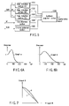
- the conversion characteristic although there is usually employed the relationship that the high-concentration side has a protruding shape as shown in a graph c of FIG.
- the black generation portion 1314 receives the low-density signals C′′M′′Y′′ outputted from the scaling processing portion 1313 .
- the black generation portion 1314 converts the low-density signals C′′M′′Y′′ into low-density signals CMYK indicative of concentrations of four colors CMYK recorded in the color printer portion 4 .
- Black (K) is used as well as CMK because a reduction in the total consumption of the toner in a dark part or improvement in a concentration and a gray level property of a dark part is intended.
- the gray scale processing portion 136 applies screen processing to the signals C′M′Y′K′ outputted from the signal switching portion 135 , converts them into the signals C′′M′′Y′′K′′ and outputs them to the color printer portion 4 .
- the gray scale is represented by using an area modulation method in many cases.
- the area modulation method there are a mode which repeatedly uses a regular pattern and a mode which uses an irregular pattern.
- the mode using a regular pattern is referred to as a screen.
- the screen there are a stripe mode which is constituted by parallel lines provided at equal intervals and represents shading by a thickness of the parallel lines, a dot mode which is constituted by a two-dimensional cyclic structure of regular dots and represents shading of a size of the dots, and a mode which switches the strips and the dots in accordance with the density. Further, as the mode using an irregular pattern, there are an error diffusion mode or a blue noise mask mode. In this embodiment, the stripe mode is employed. Furthermore, since an appropriate screen differs in a character area and a photographic area, a screen for characters and that for photographs are switched in accordance with the segmentation signal S′. The screen for characters has more fine lines and a higher representation resolution than the screen for photographs, but it has a lower stability of gray scale representation.
- FIG. 12 shows a structure of the high-resolution realization processing portion 1316 .
- the density conversion portion 1315 converts the low-density signal C′′ into the high-density signal C.
- the nearest neighbor method is used in this embodiment, the linear interpolation method or the like may be utilized like the density conversion in the first embodiment.
- a direct-current elimination filter 1316 a is applied to the high-density signal W′′. This calculates an average value in a block in units of a block of 2 ⁇ 2 pixels, subtracts the average value from each pixel value, and creates a signal. As a result, a direct-current component in the signal is eliminated, and the signal having only an alternating-current component (changed component) is outputted.
- a weighting factor 1316 b is selected by a selection portion 1316 c , and the output signal is multiplied by this factor by a multiplier 1317 . Thereafter, a result is added to the signal C which has been converted into a high-density signal by an adder 1318 , and a high-resolution realization signal C 0 is outputted.
- the high-resolution realization processing realizes the high resolution by utilizing the correlation between the low-density signals C′′M′′Y′′ and the high-density signal W′′, the correlation is generally high in the character area whilst the correlation is low in the photographic area. Therefore, when the high weighting factor is used in the photographic area, excessive correction is performed, and an ill effect such as overshoot may possibly occur, in particular, in edge portions having different hues.
- the selection portion 1316 c switches the weighting factor by using the segmentation signal, and determines the weighting factor in the photographic area as the second weighting factor “0”, thereby avoiding the above-described ill effect.
- a difference from the fourth embodiment is, as shown in FIG. 14 , that the segmentation signal S′ outputted from the segmentation portion 133 is inputted to the first filter processing portion 1312 . Moreover, the first filter processing portion 1312 stores a first filter coefficient 1312 a and a second filter coefficient 1312 b used to execute the filter processing.
Landscapes
- Engineering & Computer Science (AREA)
- Multimedia (AREA)
- Signal Processing (AREA)
- Facsimile Image Signal Circuits (AREA)
- Color Electrophotography (AREA)
- Image Processing (AREA)
- Facsimile Scanning Arrangements (AREA)
- Color Image Communication Systems (AREA)
- Color, Gradation (AREA)
Priority Applications (2)
| Application Number | Priority Date | Filing Date | Title |
|---|---|---|---|
| US10/391,755 US7324244B2 (en) | 2003-03-20 | 2003-03-20 | Image forming apparatus and image forming method |
| JP2004064037A JP2004289819A (ja) | 2003-03-20 | 2004-03-08 | 画像形成装置及び画像形成方法 |
Applications Claiming Priority (1)
| Application Number | Priority Date | Filing Date | Title |
|---|---|---|---|
| US10/391,755 US7324244B2 (en) | 2003-03-20 | 2003-03-20 | Image forming apparatus and image forming method |
Publications (2)
| Publication Number | Publication Date |
|---|---|
| US20040184104A1 US20040184104A1 (en) | 2004-09-23 |
| US7324244B2 true US7324244B2 (en) | 2008-01-29 |
Family
ID=32987755
Family Applications (1)
| Application Number | Title | Priority Date | Filing Date |
|---|---|---|---|
| US10/391,755 Expired - Fee Related US7324244B2 (en) | 2003-03-20 | 2003-03-20 | Image forming apparatus and image forming method |
Country Status (2)
| Country | Link |
|---|---|
| US (1) | US7324244B2 (enExample) |
| JP (1) | JP2004289819A (enExample) |
Cited By (4)
| Publication number | Priority date | Publication date | Assignee | Title |
|---|---|---|---|---|
| US20060082846A1 (en) * | 2004-10-20 | 2006-04-20 | Kabushiki Kaisha Toshiba | Image processing apparatus, image processing program |
| US20060209125A1 (en) * | 2005-03-16 | 2006-09-21 | Kabushiki Kaisha Toshiba | Color image processing apparatus |
| US20060209360A1 (en) * | 2005-03-16 | 2006-09-21 | Kabushiki Kaisha Toshiba | Image reading apparatus and image forming apparatus |
| US20100118322A1 (en) * | 2008-11-11 | 2010-05-13 | Canon Kabushiki Kaisha | Image forming apparatus and control method thereof |
Families Citing this family (14)
| Publication number | Priority date | Publication date | Assignee | Title |
|---|---|---|---|---|
| TWI245538B (en) * | 2004-07-28 | 2005-12-11 | Lite On Technology Corp | A high-speed image scanning system and method thereof |
| US7944593B2 (en) * | 2004-09-09 | 2011-05-17 | Infoprint Solutions Company, Llc | Method and apparatus for efficient processing of color conversion |
| JP2006256160A (ja) * | 2005-03-17 | 2006-09-28 | Fuji Xerox Co Ltd | 画像処理装置及び画像処理方法 |
| US7672019B2 (en) * | 2005-09-08 | 2010-03-02 | Kabushiki Kaisha Toshiba | Enhancing resolution of a color signal using a monochrome signal |
| US20070070444A1 (en) * | 2005-09-09 | 2007-03-29 | Kabushiki Kaisha Toshiba | Image reading apparatus and image forming apparatus |
| TWM285858U (en) * | 2005-09-16 | 2006-01-11 | Hon Hai Prec Ind Co Ltd | Network device |
| JP2008236045A (ja) * | 2007-03-16 | 2008-10-02 | Ricoh Co Ltd | 画像処理装置、画像形成装置、画像処理方法、画像処理プログラム及び記録媒体 |
| US7903302B2 (en) * | 2007-10-01 | 2011-03-08 | Kabushiki Kaisha Toshiba | Image reading apparatus and image reading method |
| JP5020904B2 (ja) * | 2008-08-05 | 2012-09-05 | 株式会社東芝 | 画像読み取り装置及びその制御方法及び画像形成装置 |
| JP5376000B2 (ja) * | 2012-03-29 | 2013-12-25 | 富士ゼロックス株式会社 | 画像読取装置および画像形成装置 |
| JP6236817B2 (ja) * | 2013-03-15 | 2017-11-29 | 株式会社リコー | 画像形成装置 |
| JP6226608B2 (ja) * | 2013-07-24 | 2017-11-08 | キヤノン株式会社 | 画像形成装置およびその制御方法 |
| CN103903588B (zh) * | 2014-03-21 | 2017-02-08 | 京东方科技集团股份有限公司 | 一种显示方法和显示系统 |
| JP6406414B2 (ja) * | 2017-11-01 | 2018-10-17 | 株式会社リコー | 画像形成装置 |
Citations (10)
| Publication number | Priority date | Publication date | Assignee | Title |
|---|---|---|---|---|
| JPS617774A (ja) | 1984-06-22 | 1986-01-14 | Toshiba Corp | カラ−画像出力装置 |
| JPS6171764A (ja) | 1984-09-17 | 1986-04-12 | Toshiba Corp | カラー画像入力装置 |
| JPS6455245U (enExample) | 1987-10-01 | 1989-04-05 | ||
| US4926251A (en) * | 1987-04-07 | 1990-05-15 | Kabushiki Kaisha Toshiba | Color image processing apparatus with image corrector |
| US20020076103A1 (en) * | 2000-12-15 | 2002-06-20 | Xerox Corporation | Method and apparatus for segmenting an image using a combination of image segmentation techniques |
| US20020094118A1 (en) * | 2001-01-16 | 2002-07-18 | Fuji Photo Film Co., Ltd. | Method and apparatus for compressing image signals |
| JP2003087556A (ja) | 2001-09-12 | 2003-03-20 | Toshiba Tec Corp | カラー信号補正回路及び画像読取装置 |
| JP2004187119A (ja) * | 2002-12-05 | 2004-07-02 | Ricoh Co Ltd | 画像処理装置および画像処理システムおよび画像処理方法 |
| US20040160651A1 (en) * | 2003-01-30 | 2004-08-19 | Toshiba Tec Kabushiki Kaisha | Image reader for use in image forming apparatus |
| US7123390B2 (en) * | 2001-09-28 | 2006-10-17 | Brother Kogyo Kabushiki Kaisha | Image scanner |
-
2003
- 2003-03-20 US US10/391,755 patent/US7324244B2/en not_active Expired - Fee Related
-
2004
- 2004-03-08 JP JP2004064037A patent/JP2004289819A/ja not_active Abandoned
Patent Citations (10)
| Publication number | Priority date | Publication date | Assignee | Title |
|---|---|---|---|---|
| JPS617774A (ja) | 1984-06-22 | 1986-01-14 | Toshiba Corp | カラ−画像出力装置 |
| JPS6171764A (ja) | 1984-09-17 | 1986-04-12 | Toshiba Corp | カラー画像入力装置 |
| US4926251A (en) * | 1987-04-07 | 1990-05-15 | Kabushiki Kaisha Toshiba | Color image processing apparatus with image corrector |
| JPS6455245U (enExample) | 1987-10-01 | 1989-04-05 | ||
| US20020076103A1 (en) * | 2000-12-15 | 2002-06-20 | Xerox Corporation | Method and apparatus for segmenting an image using a combination of image segmentation techniques |
| US20020094118A1 (en) * | 2001-01-16 | 2002-07-18 | Fuji Photo Film Co., Ltd. | Method and apparatus for compressing image signals |
| JP2003087556A (ja) | 2001-09-12 | 2003-03-20 | Toshiba Tec Corp | カラー信号補正回路及び画像読取装置 |
| US7123390B2 (en) * | 2001-09-28 | 2006-10-17 | Brother Kogyo Kabushiki Kaisha | Image scanner |
| JP2004187119A (ja) * | 2002-12-05 | 2004-07-02 | Ricoh Co Ltd | 画像処理装置および画像処理システムおよび画像処理方法 |
| US20040160651A1 (en) * | 2003-01-30 | 2004-08-19 | Toshiba Tec Kabushiki Kaisha | Image reader for use in image forming apparatus |
Cited By (7)
| Publication number | Priority date | Publication date | Assignee | Title |
|---|---|---|---|---|
| US20060082846A1 (en) * | 2004-10-20 | 2006-04-20 | Kabushiki Kaisha Toshiba | Image processing apparatus, image processing program |
| US20060209125A1 (en) * | 2005-03-16 | 2006-09-21 | Kabushiki Kaisha Toshiba | Color image processing apparatus |
| US20060209360A1 (en) * | 2005-03-16 | 2006-09-21 | Kabushiki Kaisha Toshiba | Image reading apparatus and image forming apparatus |
| US7570403B2 (en) * | 2005-03-16 | 2009-08-04 | Kabushiki Kaisha Toshiba | Color image processing apparatus |
| US7630103B2 (en) * | 2005-03-16 | 2009-12-08 | Kabushiki Kaisha Toshiba | Image reading apparatus and image forming apparatus |
| US20100118322A1 (en) * | 2008-11-11 | 2010-05-13 | Canon Kabushiki Kaisha | Image forming apparatus and control method thereof |
| US8988730B2 (en) * | 2008-11-11 | 2015-03-24 | Canon Kabushiki Kaisha | Image forming apparatus and control method thereof |
Also Published As
| Publication number | Publication date |
|---|---|
| JP2004289819A (ja) | 2004-10-14 |
| US20040184104A1 (en) | 2004-09-23 |
Similar Documents
| Publication | Publication Date | Title |
|---|---|---|
| US7324244B2 (en) | Image forming apparatus and image forming method | |
| US8259357B2 (en) | Image processing apparatus, image forming apparatus, image processing method, and computer readable recording medium | |
| JP4549418B2 (ja) | 画像処理装置、画像処理方法、画像形成装置、並びに、プログラム、記録媒体 | |
| JP3845509B2 (ja) | 画像処理装置および画像形成装置 | |
| US8477324B2 (en) | Image processor and image processing method that uses s-shaped gamma curve | |
| JP4496239B2 (ja) | 画像処理方法、画像処理装置、画像形成装置、画像読取装置、コンピュータプログラム、及び記録媒体 | |
| JPH05336373A (ja) | 画像記録装置 | |
| US7733534B2 (en) | Image processing method, image processing apparatus, image forming apparatus, and recording medium | |
| US7365880B2 (en) | Image processing apparatus and image processing method | |
| US5835238A (en) | Phantom level edge enhanced error diffusion | |
| JP4402090B2 (ja) | 画像形成装置、画像形成方法、プログラムおよび記録媒体 | |
| US8363263B2 (en) | Image processing apparatus and image processing method | |
| JP4596964B2 (ja) | 画像処理装置、画像形成装置、画像処理方法、コンピュータプログラム及び記録媒体 | |
| JP2001016442A (ja) | 画像処理方法及び装置 | |
| CN100452827C (zh) | 图像处理方法、图像处理设备和图像形成设备 | |
| JP3767210B2 (ja) | 原稿種判定装置及び画像処理装置 | |
| JP4035254B2 (ja) | 画像処理装置及び画像処理方法 | |
| JP4549227B2 (ja) | 画像処理装置、画像形成装置、画像処理方法、コンピュータプログラム及び記録媒体 | |
| JP5122507B2 (ja) | 画像処理装置、画像形成装置、画像処理方法、プログラム、記録媒体 | |
| JP4101741B2 (ja) | 画像処理装置、画像形成装置、画像処理方法、画像処理プログラム、および記録媒体 | |
| JP2951972B2 (ja) | 画像処理装置 | |
| JP4118823B2 (ja) | 画像処理装置、画像形成装置、画像処理方法、画像処理プログラム、および記録媒体 | |
| JP2941852B2 (ja) | 画像処理方法 | |
| JP2941853B2 (ja) | 画像処理方法 | |
| JPH1115968A (ja) | 画像処理装置と画像形成装置 |
Legal Events
| Date | Code | Title | Description |
|---|---|---|---|
| AS | Assignment |
Owner name: TOSHIBA TEC KABUSHIKI KAISHA, JAPAN Free format text: ASSIGNMENT OF ASSIGNORS INTEREST;ASSIGNORS:YAMAMOTO, NAOFUMI;KAWAKAMI, HARUKO;TAKANO, GAKU;REEL/FRAME:013898/0247 Effective date: 20030311 |
|
| AS | Assignment |
Owner name: TOSHIBA TEC KABUSHIKI KAISHA, JAPAN Free format text: ASSIGNMENT OF 1/2 INTEREST;ASSIGNOR:TOSHIBA TEC KABUSHIKI KAISHA;REEL/FRAME:014306/0699 Effective date: 20030717 Owner name: KABUSHIKI KAISHA TOSHIBA, JAPAN Free format text: ASSIGNMENT OF 1/2 INTEREST;ASSIGNOR:TOSHIBA TEC KABUSHIKI KAISHA;REEL/FRAME:014306/0699 Effective date: 20030717 |
|
| FPAY | Fee payment |
Year of fee payment: 4 |
|
| REMI | Maintenance fee reminder mailed | ||
| LAPS | Lapse for failure to pay maintenance fees | ||
| STCH | Information on status: patent discontinuation |
Free format text: PATENT EXPIRED DUE TO NONPAYMENT OF MAINTENANCE FEES UNDER 37 CFR 1.362 |
|
| STCH | Information on status: patent discontinuation |
Free format text: PATENT EXPIRED DUE TO NONPAYMENT OF MAINTENANCE FEES UNDER 37 CFR 1.362 |
|
| FP | Lapsed due to failure to pay maintenance fee |
Effective date: 20160129 |