US7277073B2 - Driving device, display apparatus using the same, and driving method therefor - Google Patents
Driving device, display apparatus using the same, and driving method therefor Download PDFInfo
- Publication number
- US7277073B2 US7277073B2 US10/821,480 US82148004A US7277073B2 US 7277073 B2 US7277073 B2 US 7277073B2 US 82148004 A US82148004 A US 82148004A US 7277073 B2 US7277073 B2 US 7277073B2
- Authority
- US
- United States
- Prior art keywords
- current
- voltage
- driving
- constant current
- display
- Prior art date
- Legal status (The legal status is an assumption and is not a legal conclusion. Google has not performed a legal analysis and makes no representation as to the accuracy of the status listed.)
- Expired - Fee Related, expires
Links
Images




Classifications
-
- G—PHYSICS
- G09—EDUCATION; CRYPTOGRAPHY; DISPLAY; ADVERTISING; SEALS
- G09G—ARRANGEMENTS OR CIRCUITS FOR CONTROL OF INDICATING DEVICES USING STATIC MEANS TO PRESENT VARIABLE INFORMATION
- G09G3/00—Control arrangements or circuits, of interest only in connection with visual indicators other than cathode-ray tubes
- G09G3/20—Control arrangements or circuits, of interest only in connection with visual indicators other than cathode-ray tubes for presentation of an assembly of a number of characters, e.g. a page, by composing the assembly by combination of individual elements arranged in a matrix no fixed position being assigned to or needed to be assigned to the individual characters or partial characters
- G09G3/22—Control arrangements or circuits, of interest only in connection with visual indicators other than cathode-ray tubes for presentation of an assembly of a number of characters, e.g. a page, by composing the assembly by combination of individual elements arranged in a matrix no fixed position being assigned to or needed to be assigned to the individual characters or partial characters using controlled light sources
- G09G3/30—Control arrangements or circuits, of interest only in connection with visual indicators other than cathode-ray tubes for presentation of an assembly of a number of characters, e.g. a page, by composing the assembly by combination of individual elements arranged in a matrix no fixed position being assigned to or needed to be assigned to the individual characters or partial characters using controlled light sources using electroluminescent panels
- G09G3/32—Control arrangements or circuits, of interest only in connection with visual indicators other than cathode-ray tubes for presentation of an assembly of a number of characters, e.g. a page, by composing the assembly by combination of individual elements arranged in a matrix no fixed position being assigned to or needed to be assigned to the individual characters or partial characters using controlled light sources using electroluminescent panels semiconductive, e.g. using light-emitting diodes [LED]
- G09G3/3208—Control arrangements or circuits, of interest only in connection with visual indicators other than cathode-ray tubes for presentation of an assembly of a number of characters, e.g. a page, by composing the assembly by combination of individual elements arranged in a matrix no fixed position being assigned to or needed to be assigned to the individual characters or partial characters using controlled light sources using electroluminescent panels semiconductive, e.g. using light-emitting diodes [LED] organic, e.g. using organic light-emitting diodes [OLED]
- G09G3/3216—Control arrangements or circuits, of interest only in connection with visual indicators other than cathode-ray tubes for presentation of an assembly of a number of characters, e.g. a page, by composing the assembly by combination of individual elements arranged in a matrix no fixed position being assigned to or needed to be assigned to the individual characters or partial characters using controlled light sources using electroluminescent panels semiconductive, e.g. using light-emitting diodes [LED] organic, e.g. using organic light-emitting diodes [OLED] using a passive matrix
-
- G—PHYSICS
- G09—EDUCATION; CRYPTOGRAPHY; DISPLAY; ADVERTISING; SEALS
- G09G—ARRANGEMENTS OR CIRCUITS FOR CONTROL OF INDICATING DEVICES USING STATIC MEANS TO PRESENT VARIABLE INFORMATION
- G09G3/00—Control arrangements or circuits, of interest only in connection with visual indicators other than cathode-ray tubes
- G09G3/20—Control arrangements or circuits, of interest only in connection with visual indicators other than cathode-ray tubes for presentation of an assembly of a number of characters, e.g. a page, by composing the assembly by combination of individual elements arranged in a matrix no fixed position being assigned to or needed to be assigned to the individual characters or partial characters
- G09G3/22—Control arrangements or circuits, of interest only in connection with visual indicators other than cathode-ray tubes for presentation of an assembly of a number of characters, e.g. a page, by composing the assembly by combination of individual elements arranged in a matrix no fixed position being assigned to or needed to be assigned to the individual characters or partial characters using controlled light sources
- G09G3/30—Control arrangements or circuits, of interest only in connection with visual indicators other than cathode-ray tubes for presentation of an assembly of a number of characters, e.g. a page, by composing the assembly by combination of individual elements arranged in a matrix no fixed position being assigned to or needed to be assigned to the individual characters or partial characters using controlled light sources using electroluminescent panels
-
- G—PHYSICS
- G09—EDUCATION; CRYPTOGRAPHY; DISPLAY; ADVERTISING; SEALS
- G09G—ARRANGEMENTS OR CIRCUITS FOR CONTROL OF INDICATING DEVICES USING STATIC MEANS TO PRESENT VARIABLE INFORMATION
- G09G3/00—Control arrangements or circuits, of interest only in connection with visual indicators other than cathode-ray tubes
- G09G3/20—Control arrangements or circuits, of interest only in connection with visual indicators other than cathode-ray tubes for presentation of an assembly of a number of characters, e.g. a page, by composing the assembly by combination of individual elements arranged in a matrix no fixed position being assigned to or needed to be assigned to the individual characters or partial characters
-
- G—PHYSICS
- G09—EDUCATION; CRYPTOGRAPHY; DISPLAY; ADVERTISING; SEALS
- G09G—ARRANGEMENTS OR CIRCUITS FOR CONTROL OF INDICATING DEVICES USING STATIC MEANS TO PRESENT VARIABLE INFORMATION
- G09G3/00—Control arrangements or circuits, of interest only in connection with visual indicators other than cathode-ray tubes
- G09G3/20—Control arrangements or circuits, of interest only in connection with visual indicators other than cathode-ray tubes for presentation of an assembly of a number of characters, e.g. a page, by composing the assembly by combination of individual elements arranged in a matrix no fixed position being assigned to or needed to be assigned to the individual characters or partial characters
- G09G3/22—Control arrangements or circuits, of interest only in connection with visual indicators other than cathode-ray tubes for presentation of an assembly of a number of characters, e.g. a page, by composing the assembly by combination of individual elements arranged in a matrix no fixed position being assigned to or needed to be assigned to the individual characters or partial characters using controlled light sources
- G09G3/30—Control arrangements or circuits, of interest only in connection with visual indicators other than cathode-ray tubes for presentation of an assembly of a number of characters, e.g. a page, by composing the assembly by combination of individual elements arranged in a matrix no fixed position being assigned to or needed to be assigned to the individual characters or partial characters using controlled light sources using electroluminescent panels
- G09G3/32—Control arrangements or circuits, of interest only in connection with visual indicators other than cathode-ray tubes for presentation of an assembly of a number of characters, e.g. a page, by composing the assembly by combination of individual elements arranged in a matrix no fixed position being assigned to or needed to be assigned to the individual characters or partial characters using controlled light sources using electroluminescent panels semiconductive, e.g. using light-emitting diodes [LED]
- G09G3/3208—Control arrangements or circuits, of interest only in connection with visual indicators other than cathode-ray tubes for presentation of an assembly of a number of characters, e.g. a page, by composing the assembly by combination of individual elements arranged in a matrix no fixed position being assigned to or needed to be assigned to the individual characters or partial characters using controlled light sources using electroluminescent panels semiconductive, e.g. using light-emitting diodes [LED] organic, e.g. using organic light-emitting diodes [OLED]
- G09G3/3275—Details of drivers for data electrodes
- G09G3/3283—Details of drivers for data electrodes in which the data driver supplies a variable data current for setting the current through, or the voltage across, the light-emitting elements
-
- G—PHYSICS
- G09—EDUCATION; CRYPTOGRAPHY; DISPLAY; ADVERTISING; SEALS
- G09G—ARRANGEMENTS OR CIRCUITS FOR CONTROL OF INDICATING DEVICES USING STATIC MEANS TO PRESENT VARIABLE INFORMATION
- G09G2310/00—Command of the display device
- G09G2310/02—Addressing, scanning or driving the display screen or processing steps related thereto
- G09G2310/0243—Details of the generation of driving signals
- G09G2310/0248—Precharge or discharge of column electrodes before or after applying exact column voltages
-
- G—PHYSICS
- G09—EDUCATION; CRYPTOGRAPHY; DISPLAY; ADVERTISING; SEALS
- G09G—ARRANGEMENTS OR CIRCUITS FOR CONTROL OF INDICATING DEVICES USING STATIC MEANS TO PRESENT VARIABLE INFORMATION
- G09G2310/00—Command of the display device
- G09G2310/02—Addressing, scanning or driving the display screen or processing steps related thereto
- G09G2310/0264—Details of driving circuits
- G09G2310/0297—Special arrangements with multiplexing or demultiplexing of display data in the drivers for data electrodes, in a pre-processing circuitry delivering display data to said drivers or in the matrix panel, e.g. multiplexing plural data signals to one D/A converter or demultiplexing the D/A converter output to multiple columns
-
- G—PHYSICS
- G09—EDUCATION; CRYPTOGRAPHY; DISPLAY; ADVERTISING; SEALS
- G09G—ARRANGEMENTS OR CIRCUITS FOR CONTROL OF INDICATING DEVICES USING STATIC MEANS TO PRESENT VARIABLE INFORMATION
- G09G3/00—Control arrangements or circuits, of interest only in connection with visual indicators other than cathode-ray tubes
- G09G3/20—Control arrangements or circuits, of interest only in connection with visual indicators other than cathode-ray tubes for presentation of an assembly of a number of characters, e.g. a page, by composing the assembly by combination of individual elements arranged in a matrix no fixed position being assigned to or needed to be assigned to the individual characters or partial characters
- G09G3/2007—Display of intermediate tones
- G09G3/2014—Display of intermediate tones by modulation of the duration of a single pulse during which the logic level remains constant
-
- G—PHYSICS
- G09—EDUCATION; CRYPTOGRAPHY; DISPLAY; ADVERTISING; SEALS
- G09G—ARRANGEMENTS OR CIRCUITS FOR CONTROL OF INDICATING DEVICES USING STATIC MEANS TO PRESENT VARIABLE INFORMATION
- G09G3/00—Control arrangements or circuits, of interest only in connection with visual indicators other than cathode-ray tubes
- G09G3/20—Control arrangements or circuits, of interest only in connection with visual indicators other than cathode-ray tubes for presentation of an assembly of a number of characters, e.g. a page, by composing the assembly by combination of individual elements arranged in a matrix no fixed position being assigned to or needed to be assigned to the individual characters or partial characters
- G09G3/22—Control arrangements or circuits, of interest only in connection with visual indicators other than cathode-ray tubes for presentation of an assembly of a number of characters, e.g. a page, by composing the assembly by combination of individual elements arranged in a matrix no fixed position being assigned to or needed to be assigned to the individual characters or partial characters using controlled light sources
- G09G3/30—Control arrangements or circuits, of interest only in connection with visual indicators other than cathode-ray tubes for presentation of an assembly of a number of characters, e.g. a page, by composing the assembly by combination of individual elements arranged in a matrix no fixed position being assigned to or needed to be assigned to the individual characters or partial characters using controlled light sources using electroluminescent panels
- G09G3/32—Control arrangements or circuits, of interest only in connection with visual indicators other than cathode-ray tubes for presentation of an assembly of a number of characters, e.g. a page, by composing the assembly by combination of individual elements arranged in a matrix no fixed position being assigned to or needed to be assigned to the individual characters or partial characters using controlled light sources using electroluminescent panels semiconductive, e.g. using light-emitting diodes [LED]
- G09G3/3208—Control arrangements or circuits, of interest only in connection with visual indicators other than cathode-ray tubes for presentation of an assembly of a number of characters, e.g. a page, by composing the assembly by combination of individual elements arranged in a matrix no fixed position being assigned to or needed to be assigned to the individual characters or partial characters using controlled light sources using electroluminescent panels semiconductive, e.g. using light-emitting diodes [LED] organic, e.g. using organic light-emitting diodes [OLED]
- G09G3/3266—Details of drivers for scan electrodes
Definitions
- the present invention relates to a driving device, a display apparatus using the driving device, and a driving method for the display apparatus and, more particularly, to a driving device for driving a current-driven optical element, a display apparatus for driving a simple matrix type display panel having display elements formed from a current-driven optical elements by using the driving device, and a driving method for the display apparatus.
- LCDs liquid crystal displays
- CRTs cathode-ray tubes
- LCDs liquid crystal displays
- PDAs personal digital assistants
- organic electroluminescence elements to be abbreviated as “organic EL elements” hereinafter
- inorganic electroluminescence elements to be abbreviated as “inorganic EL elements” hereinafter
- display devices having spontaneous emission type optical elements such as light-emitting diodes (LEDs).
- display devices having various kinds of spontaneous emission type display elements have recently undergone vigorous research and development toward practical application and commercialization because technical achievements superior to those obtained in other kinds of display elements have been obtained in terms of color display, low-voltage drive techniques, and the like.
- FIGS. 13A , 13 B, and 13 C respectively show the schematic arrangement of an organic EL element, its voltage-current characteristic, and an equivalent circuit of the organic EL element.
- the structure, emission principle, and emission characteristics of the organic EL element will be briefly described below.
- an organic EL element OEL has an arrangement in which an anode electrode (positive electrode) 112 made of a transparent electrode material such as ITO (Indium Thin Oxide), an organic EL layer 113 made of a light-emitting material such as an organic compound, and a cathode electrode (negative electrode) 114 made of a metal material and having a reflection characteristic are sequentially stacked on one surface of a transparent insulating substrate 111 such as a glass substrate.
- anode electrode (positive electrode) 112 made of a transparent electrode material such as ITO (Indium Thin Oxide)
- an organic EL layer 113 made of a light-emitting material such as an organic compound
- a cathode electrode (negative electrode) 114 made of a metal material and having a reflection characteristic
- the organic EL layer 113 is formed by, for example, stacking a hole transport layer 113 a made of a polymer-based hole transport material and an electron transport light-emitting layer 113 b made of a polymer-based electron transport light-emitting material.
- the organic EL element OEL As shown FIG. 13A , when positive and negative voltages are applied from a DC voltage source V DC to the anode electrode 112 and cathode electrode 114 , respectively, light h ⁇ is emitted on the basis of the energy produced when holes injected into the hole transport layer 113 a recombine with electrons injected into the electron transport light-emitting layer 113 b within the organic EL layer 113 .
- the light h ⁇ is transmitted through the anode electrode 112 and emerges from the other surface side (upper side in FIG. 13A ) of the insulting substrate 111 .
- the emission intensity (i.e., the emission luminance of the organic EL element) of the light h ⁇ is controlled in accordance with the amount of current flowing between the anode electrode 112 and the cathode electrode 114 .
- the voltage-current characteristic of an equivalent circuit of the organic EL element OEL exhibits a similar tendency to that of a diode, as shown in FIG. 13B , and the electrode layers (anode electrode 112 and cathode electrode 114 ) oppose each other through the relatively thin dielectric layer (organic EL layer 113 ).
- the optical element can be expressed as a parallel connection of a diode type light-emitting element Ep and a junction capacitance Cp. Note that the voltage-current characteristic of the organic EL element will be described in detail later in the embodiments of the present invention (to be described later).
- the active matrix driving scheme and simple matrix (passive matrix) driving scheme are known.
- a selection switch and storage capacitance are provided for each display pixel to control the driven state (emission state) of each display element in accordance with the charge voltage of a corresponding one of the storage capacitances in the simple matrix driving scheme, the emission state of each display pixel is time-divisionally controlled by directly applying a predetermined pulse to the display element.
- the active matrix driving scheme is superior to the passive one in terms of luminance and multi-gradation for image display, a pixel driving function such as a selection switch (thin-film transistor) must be provided for each display pixel. This complicates the apparatus arrangement and demands a more advanced micropatterning technique, resulting in an increase in product cost.
- a pixel driving function such as a selection switch for each display pixel, and hence the apparatus arrangement can be simplified. This makes it possible to improve the manufacturing yield and reduce the product cost.
- FIG. 14 shows an example of the display apparatus based on the simple matrix driving scheme.
- the display apparatus based on the simple matrix driving scheme is roughly comprised of a display panel 110 P having a plurality of scanning lines SL extended in a row direction, a plurality of signal lines DL extended in a column direction to intersect the scanning lines SL at right angles, and display elements (organic EL elements) OEL each formed near the intersection of the scanning line SL and the signal line DL.
- the apparatus further includes a scanning driver 120 P which applies a scanning signal to each scanning line SL at a predetermined timing to sequentially scan the organic EL elements OEL on each row in the selected state, a data driver 130 P which generates a driving current corresponding to display data and supplies the current to each organic EL element OEL through a corresponding one of the signal lines DL in synchronism with scanning by the scanning driver 120 P, and a controller 140 P which generates a scanning control signal, data control signal, and display data which are used to display desired image information on the display panel 110 P, and supplies them to the scanning driver 120 P and data driver 130 P.
- a scanning driver 120 P which applies a scanning signal to each scanning line SL at a predetermined timing to sequentially scan the organic EL elements OEL on each row in the selected state
- a data driver 130 P which generates a driving current corresponding to display data and supplies the current to each organic EL element OEL through a corresponding one of the signal lines DL in synchronism with scanning by the scanning driver
- One method is a current designation type driving method in which the scanning driver 120 P sequentially applies a scanning signal for selecting one of the scanning lines SL to the scanning line SL of each row on the basis of a scanning control signal supplied from the controller 140 P in each predetermined scanning period, and the data driver 130 P generates a driving current having a predetermined current value corresponding to display data in the scanning period on the basis of a data control signal and display data supplied from the controller 140 P in synchronism with this scanning signal, and simultaneously supplies driving currents through the respective signal lines DL.
- the respective organic EL elements OEL on a selected row emit light with a predetermined luminance level.
- the other method is a pulse width modulation type driving method in which the data driver 130 P generates a driving current formed from a constant current value and having a signal time width (pulse signal width) corresponding to display data, and supplies the current to each signal line DL.
- the respective organic EL elements OEL on a selected row emit light with a predetermined luminance level. This operation is sequentially repeated for each row corresponding to one frame on the display panel to display desired image information on the display panel 110 P.
- a voltage driving scheme of driving each display element by applying a predetermined voltage from the data driver to the display element is known in addition to the above current driving scheme.
- the organic EL element is used as a display element.
- each element has an arrangement in which the diode type light-emitting element Ep and junction capacitance Cp are connected in parallel as shown in FIG. 14 , and each organic EL element OEL is connected in parallel with the signal line DL, the total sum of junction capacitances becomes large, and the interconnection capacitance of each signal line is added.
- the current driving scheme is regarded superior to the voltage driving scheme.
- the display apparatus based on the above simple matrix driving scheme has the following problems.
- operating a display element with a predetermined luminance level by supplying a predetermined driving current to it is equivalent to charging the junction capacitance or the like of a given display element with a driving current and also charging the junction capacitance of the remaining unselected display elements on a signal line to which the given display element is connected.
- a deterioration in response characteristic or the occurrence of variations in emission luminance can be suppressed by supplying a driving current having a large current value.
- the driving current supplied from the data driver is set to a relatively small current value for the sake of the specifications of a power supply or power saving, or the total sum of the junction capacitances of display elements increases as the number of scanning lines increases and the number of display pixels increases along with increases in the size and resolution of a display panel.
- the driving current is supplied to the display element at a driving timing, the response characteristics with respect to current and voltage values deteriorate, and the time required for a voltage applied to the display element to reach a predetermined value is prolonged, resulting in a noticeable lack of emission luminance and occurrence of variations.
- FIG. 15A shows a change in supply current over time when a driving current is supplied to a display element.
- FIG. 15B shows a change in voltage applied to a display element over time.
- the abscissa represents the time; and, the ordinate, the supply current to the display element.
- Reference symbol Tspy denotes a supply period of a driving current; and Tdly, a delay time from the start of supply of the driving current to the start of operation of the display element.
- the abscissa represents the time; and the ordinate, the voltage applied to a display pixel in the forward direction.
- Reference symbol Vth denotes a threshold voltage for operation in the display element. As shown in FIGS.
- the rise characteristics of a current value and voltage value supplied to the display element deteriorate owing to the junction capacitance of the display element and the interconnection capacitance of a signal line.
- the degree of deterioration varies.
- the amount of electric charges supplied to the display element in a driving current supply period decreases below the amount required for display with a desired luminance level, resulting in a lack of emission luminance or variations in emission luminance among the display elements. This leads to a deterioration in display state.
- the response speed of each optical element can be increased, and hence each optical element can be properly driven even if a driving current to be supplied to each optical element is set to a relatively small current value.
- the response speed of each display element in the entire area of the display panel is increased to obtain good display image quality in accordance with a display gray level, and the power consumption associated with supply of a driving current to each display element can be reduced.
- a driving device which supplies a current to a plurality of current-driven optical elements to drive the optical elements, comprising at least a driving current supply circuit which supplies a driving current to each optical element for a predetermined period, and a control voltage applying circuit which applies at least a charge voltage having a voltage value corresponding to a voltage to be applied to each optical element using the driving current, before the driving current is supplied.
- the driving current supplied to each optical element has the same current value with respect to each optical element.
- the driving current supply circuit comprises a single constant current generating circuit which outputs a constant current having the same current value as that of the driving current, and a plurality of current storage circuits which sequentially receive and hold the constant current and output the driving current on the basis of the constant current.
- the driving current supply circuit further comprises a single input current storage circuit which is provided between the constant current generating circuit and the plurality of current storage circuits, receives the constant current output from the constant current generating circuit, holds a voltage component corresponding to a current value of the constant current, and supplies a current based on the voltage component to the plurality of current storage circuits.
- the input current storage circuit and each of the current storage circuits include a capacitance element which receives the constant current output from the constant current generating circuit and in which electric charge corresponding to a current value of the constant current is written as a voltage component.
- the control voltage applying circuit further comprises means for applying a discharge voltage having a voltage value for causing each optical element to perform discharging operation, after the driving current is supplied to each optical element.
- the driving device also comprises a pulse width control circuit which controls a pulse width of the driving current applied to each optical element in accordance with a luminance level component of a display signal.
- a display apparatus which displays image information by supplying a driving current corresponding to a display signal to each of a plurality of current-driven display elements of a display panel, comprising a display panel including a plurality of signal lines and a plurality of scanning lines intersecting at right angles, and the plurality of display elements arranged near intersections of the signal lines and the scanning lines, a scanning control circuit which sequentially scans the scanning lines to sequentially set the display elements connected to the scanning lines in a selected state, and a signal control circuit including at least a driving current supply circuit which supplies a driving current to each signal line for a predetermined period, and a control voltage applying circuit which applies, to each signal line, a charge voltage having a voltage value based on a voltage applied to each display element upon application of the driving current, before supply of the driving current.
- the display element comprises an optical element, which is, for example, an organic electroluminescence element, the organic electroluminescence element having an anode electrode connected
- the charge voltage has at least a voltage value which is higher than a threshold voltage for each display element of the display panel and smaller than a maximum value of a voltage value applied to each display element when the driving current is supplied to each display element through each signal line.
- the charge voltage has a voltage value equal to an average value of voltage values applied to the respective display elements when the driving current is supplied to the respective display elements through the respective signal lines.
- the driving current supplied to each signal line of the display panel has the same current value for each signal line.
- the signal control circuit comprises at least a control section which performs supply of the driving current by the driving current supply circuit and application of the charge voltage by the control voltage applying circuit in accordance with a timing at which the scanning control circuit sets the display element in a selected state.
- the driving current supply circuit in the signal control circuit comprises a single constant current generating circuit which outputs a constant current having a predetermined current value, and a plurality of current storage circuits which are provided in correspondence with the plurality of signal lines, sequentially receive and hold the constant current, and simultaneously output the driving currents to the plurality of signal lines on the basis of the constant current.
- the driving current supply circuit further comprises a single input current storage circuit which is provided between the constant current generating circuit and the plurality of current storage circuits, receives the constant current output from the constant current generating circuit, holds a voltage component corresponding to a current value of the constant current, and supplies a current based on the voltage component to the plurality of current storage circuits.
- the current storage circuit and input current storage circuit each include a capacitance element which receives the constant current output from the constant current generating circuit and in which electric charge corresponding to the constant current is written as the voltage component.
- the control voltage applying circuit in the signal control circuit further comprises means for applying, to each signal line, a discharge voltage which causes each display element to perform discharging operation and does not exceed a threshold voltage of the display element, after the driving current is supplied to each signal line.
- the signal control circuit comprises a pulse width control circuit which controls a pulse width of the driving current to each signal line in accordance with a luminance level component of a display signal.
- FIG. 1 is a block diagram showing an example of the overall arrangement of a driving device and a display apparatus using the driving device;
- FIG. 2 is a schematic circuit diagram showing the arrangement of a part of the display apparatus to which the present invention can be applied;
- FIG. 3 is a circuit diagram showing the arrangement of a part of a data driver which can be applied to the driving device according to the present invention
- FIG. 4 is a timing chart showing control operation in a scanning driver and the data driver which can be applied to the present invention
- FIG. 5 is a graph showing voltage-current characteristics representing the relationship between voltages applied by the scanning driver and data driver which can be applied to the present invention
- FIG. 6 is a timing chart showing display driving operation in the display apparatus to which the present invention can be applied.
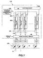
- FIG. 7 is a schematic block diagram showing a first embodiment of a constant current supply circuit which can be applied to the driving apparatus according to the present invention.
- FIG. 8 is a circuit diagram showing a specific example of a current generating circuit which can be applied to the constant current supply circuit according to the present invention.
- FIG. 9 is a circuit diagram showing a specific example of an arrangement constituted by a current storage circuit and switch means which can be applied to the constant current supply circuit according to the present invention.
- FIGS. 10A and 10B are circuit diagrams showing basic operation in a current storage circuit which can be applied to the constant current supply circuit according to the present invention
- FIG. 11 is a schematic block diagram showing a second embodiment of the constant current supply circuit which can be applied to the driving device according to the present invention.
- FIG. 12 is a schematic block diagram showing a third embodiment of the constant current supply circuit which can be applied to the driving device according to the present invention.
- FIG. 13A is a sectional view showing the schematic arrangement of an organic EL element
- FIG. 13B is a graph showing the approximate voltage-current characteristic of the organic EL element
- FIG. 13C is an equivalent circuit diagram of the organic EL element
- FIG. 14 is a view showing an example of a display apparatus based on the simple matrix driving scheme
- FIG. 15A is a graph showing a change in supply current over time when a driving current is supplied to an organic EL element.
- FIG. 15B is a graph showing a change in voltage applied to a display element over time when a driving current is supplied to an organic EL element.
- Embodiments of a driving device, a display apparatus using the driving device, and a driving method for the display apparatus according to the present invention will be described in detail below.
- FIG. 1 is a block diagram showing an example of the overall arrangement of the driving device according to the present invention and the display apparatus to which the driving device can be applied.
- FIG. 2 is a schematic circuit diagram showing the arrangement of the main part of the display apparatus to which the present invention can be applied.
- organic EL elements OEL are used as display elements for a display panel.
- the display apparatus according to the present invention is not limited to this.
- the present invention can also be suitably applied to a case wherein optical elements such as light-emitting diodes (LEDs) are used as display elements instead of organic EL elements.
- LEDs light-emitting diodes
- a display apparatus 100 to which the present invention can be applied is comprised of a display panel (pixel array) 110 , scanning driver (scanning control circuit) 120 , data driver (signal control circuit) 130 , system controller 140 , and display signal generating circuit 150 .
- display elements including, for example, organic EL elements OEL are formed near the intersections of a plurality of scanning lines SL and a plurality of signal lines DL which are arranged in orthogonal directions.
- the scanning driver 120 is connected to the scanning lines SL of the display panel 110 and controls the display elements on each row in the selected state by sequentially applying a scanning signal Vs to each scanning line SL at a predetermined timing.
- the data driver 130 is connected to the signal lines DL of the display panel 110 , supplies a constant current (driving current) Ic having a signal time width (pulse width) corresponding to display data in synchronism with the application timing of the scanning signal Vs, and applies a set voltage Vset (charge voltage) or reset voltage Vreset (discharge voltage) at a predetermined timing.
- the system controller 140 generates and outputs at least a scanning control signal and data control signal for controlling the operation states of the scanning driver 120 and data driver 130 , on the basis of a timing signal supplied from the display signal generating circuit 150 .
- the display signal generating circuit 150 supplies the above display data to the data driver 130 on the basis of a video signal supplied from the outside of the display apparatus 100 , generates a timing signal (system clock or the like) for operating each organic EL element in a predetermined driven state on the basis of the display data, and supplies the timing signal to the system controller 140 .
- a timing signal system clock or the like
- the display panel 110 which can be applied to the present invention has n scanning line SL and m signal lines DL which are intersecting each other at right angles.
- the display panel 110 has a simple matrix arrangement in which the organic EL elements OEL each having the cross-sectional structure shown in FIG. 13A are formed at the intersections of the respective signal lines DL and the respective scanning lines SL with the anode electrodes (positive electrodes) and cathode electrodes (negative electrodes) of the elements being connected to the signal lines DL and the scanning lines SL, respectively.
- each organic EL element OEL has an arrangement in which a diode type display element Ep and a junction capacitance Ca are connected in parallel as in FIG. 14 .
- the scanning driver 120 is comprised of a shift register 121 , switches SWL 1 , SWL 2 , . . . , SWLn (to be also referred to as “switches SWL” herein after for the sake of convenience), high-voltage power supply, and low-voltage power supply.
- the shift register 121 sequentially outputs shift output signals RS 1 , RS 2 , . . . , RSn (to be also referred to as “shift output signals RS” hereinafter for the sake of convenience) on the basis of scanning control signals (a shift start signal, shift clock, and the like) supplied from the system controller 140 .
- the high-voltage power supply commonly applies a signal voltage Vsh (charge control voltage) of a predetermined high voltage (high level) to one of the switching contacts of each of the switches SWL 1 , SWL 2 , . . . , SWLn.
- the low-voltage power supply commonly applies a signal voltage Vs 1 (driving control voltage) of a predetermined low voltage (low level) to the other of the switching contacts of each of the switches SWL 1 , SWL 2 , . . . , SWLn.
- the switching contacts are sequentially switched to the low-voltage power supply side.
- the scanning signal Vs having the low-level signal voltage Vs 1 is applied to the anode electrodes of the organic EL elements OEL on the selected row (scanning line) for only a predetermined period (the supply period of the driving current Ic and the application period of the reset voltage Vreset in one scanning period).
- each switch SWL is formed from a switch element such as a field-effect transistor.
- FIG. 3 is a circuit diagram showing the arrangement of the main part of the data driver which can be applied to the driving device according to the present invention.
- the data driver 130 sequentially receives and holds display data line by line supplied from the display signal generating circuit 150 at a predetermined timing on the basis of various data control signals (an output enable signal, output control signal, shift start signal, shift clock, and the like) supplied from the system controller 140 .
- the data driver 130 converts each display data into a current component of a constant value with a signal time width (pulse width) corresponding to the luminance level of the display data, and supplies the data to each signal line DL at a predetermined timing within a scanning period set for each of the above scanning lines.
- the data driver 130 is comprised of a control section 131 , switches SWC 1 , SWC 2 , . . . , SWCm (to be also referred to as “switches SWC” hereinafter for the sake of convenience), a control voltage applying circuit 132 , and constant current supply circuits 133 (driving current supply circuits).
- the control section 131 outputs control signal CS 1 , CS 2 , . . . , CSm in accordance with a timing at which the scanning driver 120 sets display elements on each row in the selected state by applying the scanning signal Vs to each scanning line SL on the basis of data control signals (output control signals and the like) supplied from the system controller 140 .
- the switches SWC 1 , SWC 2 , . . . , SWCm are provided for the respective signal lines DL, and the contacts of the switches are switched on the basis of control signal CS 1 , CS 2 , . . . , CSm supplied from the control section 131 .
- the control voltage applying circuit 132 commonly applies the set voltage Vset (charge voltage) of a predetermined high voltage (high level) to the first switching contacts of the switches SWC 1 , SWC 2 , . . . , SWCm, and commonly applies the reset voltage Vreset (discharge voltage) of a predetermined low voltage (low level) to the third switching contacts of the switches SWC 1 , SWC 2 , . . . , SWCm.
- the set voltage Vset is set to a value corresponding to a potential to be applied to the display element by supplying the constant driving current Ic and that is equal to or more than at least the threshold voltage of the display element and does not exceed the maximum voltage applied to each display element when the driving current Ic is supplied. More preferably, the set voltage Vset is set to the average voltage of the maximum voltage and minimum voltage at the signal line DL when the driving current Ic is supplied.
- the reset voltage Vreset is set to a value that can temporarily release and reset the charge of the signal line DL and, for example, set to ground potential (0 V). More preferably the reset voltage Vreset is set to be slightly lower than the threshold voltage of the display element.
- Each of the constant current supply circuits 133 supplies the driving current Ic having a constant current value and a signal time width (pulse width) based on the luminance graduation component of display data to the second switching contact of a corresponding one of the switches SWC 1 , SWC 2 , . . . , SWCm.
- a constant current supply circuit which can be applied to the data driver according to the present invention will be described in detailed later.
- FIG. 3 is a circuit diagram showing an example of an arrangement of the switches SWC which can be applied to the data driver 130 .
- each of the switches SWC 1 , SWC 2 , . . . , SWCm provided for the respective signal lines DL of the data driver 130 can have an arrangement including a switch element (to be referred to as an “NMOS transistor” hereinafter) Tr 11 , NMOS transistor Tr 12 , and switch element (to be referred to as a “PMOS transistor” hereinafter) Tr 13 .
- NMOS transistor NMOS transistor
- the NMOS transistor Tr 11 is formed from an n-channel field-effect transistor and has a source terminal connected to the high-voltage power applying circuit 132 for applying the constant set voltage Vset, a drain terminal connected to the signal line DL, and a gate terminal to which a control signal Vgs is applied at the first timing.
- the NMOS transistor Tr 12 has a source terminal connected to the constant current supply circuit 133 for supplying the constant driving current Ic, a drain terminal connected to the signal line DL, and a gate terminal to which a control signal Vgc is applied at the second timing.
- the PMOS transistor Tr 13 is formed from a p-channel field-effect transistor and has a source terminal connected to the low-voltage power applying circuit 134 for applying the constant reset voltage Vreset, a drain terminal connected to the signal line DL, and a gate terminal to which a control signal Vgr is applied at the third timing.
- the switches SWC 1 , SWC 2 , . . . , SWCm each have an arrangement in which the NMOS transistors Tr 11 and Tr 12 and PMOS transistor Tr 13 are connected in parallel with the single signal line DL.
- the switches SWC 1 , SWC 2 , . . . , SWCm are selectively turned on at different timings to supply predetermined voltages or currents to the signal lines DL.
- the control signals Vgs, Vgc, and Vgr applied to the gate terminals of the NMOS transistors Tr 11 and Tr 12 and the PMOS transistor Tr 13 are generated on the basis of data control signals supplied from the system controller 140 and display data supplied from the display signal generating circuit 150 , and are selectively applied to the respective transistors at predetermined timings within a scanning period set for each row (scanning line).
- the operations of these switches SWC 1 , SWC 2 , . . . , SWCm and voltage and current components supplied to the signal lines DL will be described in detail later.
- resistance components Rpa, Rp, and Rpb formed in series with the signal line DL are equivalent representations of the interconnection resistances of the signal line DL, and capacitance components Cpa and Cpb formed on the two ends of the signal line DL are interconnection capacitances (parasitic capacitances) which are parasitic on the signal line DL.
- the system controller 140 generates and outputs, to the scanning driver 120 and data driver 130 , a scanning control signal and data control signal for controlling their operation states to make the respective drivers operate at predetermined timings so as to generate and output the scanning signal Vs, driving current Ic, set voltage Vset, and reset voltage Vreset.
- the system controller 140 then supplies the scanning signal Vs to the cathode electrode of each organic EL element, and the driving current Ic, set voltage Vset, and reset voltage Vreset to the anode electrode of each organic EL element to make each organic EL element operate with a predetermined luminance level so as to display image information based on a predetermined video signal on the display panel 110 .
- the display signal generating circuit 150 extracts luminance level signal components from a video signal supplied from, for example, the outside of the display apparatus, and supplies the signal components as display data to the data driver 130 for each line of the display panel 110 .
- the display signal generating circuit 150 may have the function of extracting a timing signal component and supplying it to the system controller 140 as well as the function of extracting the above luminance level signal component.
- the system controller 140 described above generates a scanning control signal and data control signal to be respectively supplied to the scanning driver 120 and data driver 130 , on the basis of timing signals supplied from the display signal generating circuit 150 .
- FIG. 4 is a timing chart showing the control operations (driving method) of the scanning driver and data driver which can be applied to the present invention.
- FIG. 5 is a graph showing voltage-current characteristics representing the relationship between the voltages applied from the scanning driver and data driver which can be applied to the present invention.
- FIG. 6 is a timing chart showing the display driving operation of the display apparatus to which the present invention can be applied.
- a set period Tset during which the above set voltage Vset (charge voltage) is applied to each signal line DL, a constant current supply period Tc during which the driving current Ic is supplied to each signal line DL, and a reset period Treset during which the reset voltage Vreset (discharge voltage) is applied to each signal line DL are sequentially set within a scanning period Tsel (selection period) which is set for each scanning line at different timings.
- Tsel selection period
- the high-level set control signal Vgs is applied to the gate terminal of the NMOS transistor Tr 11 provided in the data driver 130 to turn on the transistor, and the reset high-level control signal Vgr is applied to the gate terminal of the PMOS transistor Tr 13 to turn off the transistor.
- the low-level current supply control signal Vgc is applied to the gate terminal of the NMOS transistor Tr 12 to keep it off.
- the set voltage Vset is set to a value corresponding to a potential (Vc) to be applied to the display element by supplying the constant driving current Ic to the signal line DL during the constant current supply period Tc (to be described later). That is, as shown in FIG. 5 , when the driving current Ic is applied to the signal line DL, a voltage drop Vdrop occurs in accordance with the interconnection length from the data driver 130 serving as a power supply to the organic EL element OEL. As a consequence, a maximum voltage Vmax is applied to the side nearest to the data driver 130 and a minimum voltage Vmin is applied to the side farthest from the data driver 130 .
- the set voltage Vset is set to a value that is equal to or more than at least the threshold voltage (turn-on voltage) of the organic EL element OEL and does not exceed the maximum voltage Vmax applied to each display element when the driving current Ic is supplied.
- the set voltage Vset is set to a voltage that can supply the driving current Ic having a constant current value to the organic EL element OEL in the central area of the display panel 110 , i.e., the average voltage of the maximum voltage Vmax and minimum voltage Vmin at the signal line DL.
- the scanning signal Vs is set to be higher in voltage than the voltage (Vmax ⁇ Vturn-on) obtained by subtracting a turn-on voltage Vturn-on for the organic EL element OEL from the maximum voltage value ( ⁇ Vmax) applied to the signal line DL.
- Vs ( Vsh )> V max ⁇ Vt run-on (1)
- this potential difference causes no current to flow in any of the organic EL elements.
- the high-level current supply control signal Vgc is applied to the gate terminal of the NMOS transistor Tr 12 to turn it on.
- the high-level reset control signal Vgr is applied to the gate terminal of the PMOS transistor Tr 13 to keep it off.
- the driving current Ic supplied from the data driver 130 to the organic EL element OEL through the signal line DL is set to be supplied with a predetermined signal time width (pulse width) corresponding to the luminance level based on display data supplied from the display signal generating circuit.
- the voltage Vc e.g., 12 V
- the predetermined driving current Ic required to perform light emission is supplied to each organic EL element connected to the selected scanning line at a predetermined signal time width (for a short period of time when the gray level is low, and vice versa) corresponding to display data on the basis of a known pulse width modulation (PWM driving) control method.
- PWM driving pulse width modulation
- the driving current Ic increases to the current value required for light emission in a very short period of time after the driving current Ic is supplied, and each organic EL element quickly emits light.
- the low-level reset control signal Vgr is applied to the gate terminal of the PMOS transistor Tr 13 to turn it on.
- the low-level set control signal Vgs is applied to the gate terminal of the NMOS transistor Tr 11 to keep it off.
- the above series of operation periods are set within a scanning period for each scanning line constituting the display panel, as shown in FIG. 6 , thereby performing grayscale display of predetermined image information based on display data on the display panel.
- the set voltage Vset is applied from the constant voltage source to the signal line DL in a scanning period before the supply of the driving current Ic to charge the interconnection capacitance added to the signal line DL and the junction capacitance of the organic EL element in advance.
- This makes it possible to quickly perform charging/discharging operation in a short period of time as compared with a case wherein the capacitances are charged by using only a constant current source.
- the apparatus is resistant to the influence of a voltage drop due to the interconnection length of the signal line DL and the like, and can be charged to the substantially uniform set voltage Vset regardless of the layout positions of the scanning lines SL in the display panel 110 .
- the set voltage Vset is approximated at the voltage Vc that is set to supply a driving current to the organic EL element. Even if, therefore, the set period Tset switches to the constant current supply period Tc to supply the constant driving current Ic, the amount of adjustment of the signal line voltage Vd 1 can be decreased. This makes it possible to shorten the time required for this adjustment and improve the response display characteristics.
- the potentials of all the scanning lines SL are set to the voltage Vsh having a predetermined high level. Even if, therefore, the set voltage Vset is applied to the signal line DL, no current flows in any organic EL element. This shortens the time required for precharging (charging) operation to the set voltage Vset, thereby improving the response characteristics.
- supplying the driving current Ic having a constant current value from the constant current source can compensate for a voltage drop at the signal line DL so as to ensure the predetermined voltage Vc. This makes it possible to properly cope with a change in voltage applied to the organic EL element OEL over time and supply the constant current (driving current) Ic based on the substantially uniform voltage Vc to the organic EL element OEL, thereby realizing high display image quality without variations in luminance level.
- the pulse width modulation control scheme of supplying the driving current Ic having a constant current value with a time signal width (pulse width) corresponding to the luminance level component contained in display data is used for each organic EL element OEL, it suffices if the driving current Ic to be supplied to each organic EL element during the constant current supply period Tc has a constant current value.
- the driving current Ic to be supplied to each organic EL element during the constant current supply period Tc has a constant current value.
- simple circuit arrangements can be used as a constant current source and constant voltage source which are used to supply the above current and voltage.
- the voltage value of the reset voltage Vreset applied to the signal line DL need not be set to ground potential (0 V) but may be set to an arbitrary voltage equal to or less than the turn-on voltage Vturn-on for the organic EL element OEL. Therefore, the amount of electric charge to be charged/discharged with respect to the interconnection capacitance or the junction capacitance of the organic EL element OEL can be reduced by the potential difference (Vreset ⁇ Vturn-on). This makes it possible to reduce power consumption.
- the reset voltage Vreset is applied to the signal line DL instead of resetting all the scanning lines SL including unselected scanning lines every time the constant current supply period Tc (reset period) terminates. This eliminates the necessity to perform charging/discharging operation for the junction capacitance of the organic EL element OEL, thus reducing power consumption.
- FIG. 7 is a schematic block diagram showing a first embodiment of the constant current supply circuit which can be applied to the data driver according to the above embodiment.
- the constant current supply circuit 133 is comprised of a single constant current generating circuit 10 A, a shift register 20 A, a plurality of switch means 40 A, a plurality of current storage circuits 30 A, and a PWM control circuit 80 .
- the constant current generating circuit 10 A generates the driving current Ic for operating a plurality of loads (organic EL elements OEL).
- the shift register 20 A sets timings at which the constant currents Ip supplied from the constant current generating circuit 10 A are sequentially supplied to the current storage circuits 30 A.
- the plurality of switch means 40 A control the supply states of the constant currents Ip to the respective current storage circuits 30 A in accordance with a switching signal (shift output) SR output from the shift register 20 A at a predetermined timing.
- the plurality of current storage circuits 30 A sequentially receive and hold (store) the constant currents Ip supplied from the constant current generating circuit 10 A through the switch means 40 A at predetermined timings based on the shift register 20 A.
- the PWM control circuit 80 is connected to output terminals Tout, receives display data, and sets a signal time width (pulse width) with which the driving current Ic is to be supplied by PWM control based on the luminance level component contained in the display data.
- SWC in FIG. 7 corresponds to the switch SWC in FIG. 2 , and is a three-contact switch provided among an output terminal of the PWM control circuit 80 , the set voltage Vset, the reset voltage Vreset, and the signal line DL connected to the plurality of organic EL elements OEL.
- FIG. 8 is a circuit diagram showing the arrangement of a specific example of the current generating circuit which can be applied to the above constant current supply circuit or circuit 10 A.
- the constant current generating circuit 10 A is designed to generate the constant current Ip having a current value required to make each of the organic EL elements operate in a predetermined emission state and output the current to each current storage circuit 30 A provided in correspondence with a corresponding one of the organic EL elements.
- the constant current generating circuit 10 A can have a circuit arrangement including a control current generating circuit 11 on the front stage and an output current generating circuit 12 on the rear stage, as shown in, for example, FIG. 8 .
- the current generating circuit described in this embodiment is merely an example that can be applied to the driving device according to the present invention, and is not limited to this circuit arrangement.
- This embodiment exemplifies, as the constant current generating circuit 10 A, the arrangement having the control current generating circuit 11 and output current generating circuit 12 .
- the present invention is not limited to this.
- a circuit having a circuit arrangement formed from only the control current generating circuit 11 may also be used.
- the control current generating circuit 11 has a circuit arrangement including a pnp bipolar transistor (to be abbreviated as a “pnp transistor” hereinafter) Q 11 and NMOS transistor M 11 .
- the pnp transistor has an emitter connected to the other terminal of a resistor R 11 whose one terminal is connected to a high-potential power supply Vdd, and a collector connected to the rear-stage current mirror circuit section 12 (output node N 11 ).
- the NMOS transistor M 11 has a source connected to the base of the pnp transistor Q 11 , a drain connected to the set terminal Tset to which a set signal SET is input, and a gate connected to an input terminal Tin to which a predetermined control signal IN is input.
- the output current generating circuit 12 has a circuit arrangement including an npn bipolar transistor (to be abbreviated as an “npn transistor” hereinafter) Q 12 , resistor R 12 , npn transistor Q 13 , and resistor R 13 .
- the npn transistor Q 12 is formed from a current mirror circuit and has a collector and base which are connected to the output node N 11 of the control current generating circuit 11 .
- the resistor R 12 is connected between the emitter of the npn transistor Q 12 and a low-potential power supply Vss.
- the npn transistor Q 13 has a collector connected to an output terminal Tcs which outputs an output current (constant current Ip) having a predetermined current component, and a base connected to the output node N 11 of the control current generating circuit 11 .
- the resistor R 13 is connected between the emitter of the npn transistor Q 13 and the low-potential power supply Vss.
- an output current (constant current Ip) has a current value corresponding to a predetermined current ratio which is defined by the current mirror circuit arrangement with respect to the current value of a control current generated by the control current generating circuit 11 and input through the output node N 11 .
- a current component flows from the current storage circuit 30 A to the constant current generating circuit 10 A.
- the shift register 20 A sequentially applies sequentially output shift outputs as switching signals SR to the respective switch means 40 A provided in correspondence with the respective signal lines DL on the basis of control signals supplied from, for example, a control section such as the system controller 140 shown in FIG. 1 .
- the switch means 40 A are turned on at different timings on the basis of the switching signals SR output from the shift register 20 A to supply the constant currents Ip from the constant current generating circuit 10 A to the current storage circuits 30 A so as to control them to receive and hold the currents.
- FIG. 9 is a circuit diagram showing an example of an arrangement including a current storage circuit and a switch means which can be applied to the above constant current supply circuit.
- FIGS. 10A and 10B are conceptual views showing the basic operation of a current storage circuit which can be applied to the above constant current supply circuit.
- the current storage circuits 30 A are designed to sequentially receive and hold the constant currents Ip output from the constant current generating circuit 10 A on the basis of shift outputs output from the shift register 20 A and simultaneously output the held current components directly or predetermined currents generated on the basis of the current components, as the driving currents Ic, to the respective signal lines DL through the output terminals Tout.
- the current storage circuit 30 A can have a circuit arrangement including a voltage component holding section 31 (including the switch means 40 A) on the front stage and a driving current generating section 32 on the rear stage, as shown in, for example, FIG. 9 .
- the current storage circuit described in this embodiment is merely an example that can be applied to the driving device according to the present invention, and is not limited to this circuit arrangement.
- This embodiment exemplifies, as the current storage circuit 30 A, the arrangement having the voltage component holding section 31 and driving current generating section 32 .
- the present invention is not limited to this.
- a circuit having a circuit arrangement formed from only the voltage component holding section 31 may also be used.
- the voltage component holding section 31 has an arrangement including PMOS transistors M 31 , M 32 , and M 33 , storage capacitance C 31 , and PMOS transistor M 34 .
- the PMOS transistor M 31 has a source and drain respectively connected to a node N 31 and an output terminal Tcs of the constant current generating circuit 10 A, and a gate connected to an shift output terminal Tsr of the shift register.
- the PMOS transistor M 32 has a source and drain respectively connected to a high-potential power supply Vdd and a node N 32 , and a gate connected to the node N 31 .
- the PMOS transistor M 33 has a source and drain respectively connected to the node N 32 and the output terminal Tcs of the constant current generating circuit 10 A, and a gate connected to the shift output terminal Tsr of the shift register 20 A.
- the storage capacitance C 31 is connected between the high-potential power supply Vdd and the node N 31 .
- the PMOS transistor M 34 has a source and drain respectively connected to the node N 32 and an output node N 33 of the rear-stage driving current generating section 32 , and a gate connected to an output control terminal Ten to which an output enable signal EN which is supplied from a control section such as the system controller 140 shown in FIG. 1 and controls the output state of a control current to the rear-stage driving current generating section 32 is input.
- the PMOS transistors M 31 and M 33 which are turned on/off on the basis of the switching signals (shift outputs) SR from the shift register 20 A constitute the switch means 40 A described above.
- the storage capacitance C 31 provided between the high-potential power supply Vdd and the node N 31 may be a parasitic capacitance formed between the gate and source of the PMOS transistor M 32 .
- the driving current generating section 32 comprises a current mirror circuit and has an arrangement including npn transistors Q 31 , Q 32 , and Q 33 , and resistors R 31 and R 32 .
- the npn transistors Q 31 and Q 32 have collectors and bases connected to the output node N 33 of the voltage component holding section 31 described above, and emitters connected to a node N 34 .
- the resistor R 31 is connected between the node N 34 and a low-potential power supply Vss.
- the npn transistor Q 33 has a collector connected to a high-potential power supply Vdd and a base connected to the output node N 33 of the voltage component holding section 31 described above.
- the resistor R 32 is connected between an emitter of the npn transistor Q 33 and an output terminal Tout from which an output current (driving current Ic) is output.
- the output current (driving current Ic) has a current value corresponding to a predetermined current ratio defined by the current mirror circuit arrangement with respect to the current value of a control current output from the voltage component holding section 31 and input through the output node N 33 .
- the above current ratio may be defined by changing the area ratios among the npn transistors Q 31 to Q 33 instead of using the resistors R 31 and R 32 which define the current ratio in the circuit arrangement of the current mirror circuit 32 .
- variations in output current can be suppressed by suppressing the occurrence of variations in current component inside the circuit due to variations in the resistance values of the resistors R 31 and R 32 .
- current holding operation and current supplying operation are executed at predetermined timings, in an operation cycle (scanning period) of the organic EL element, so as not to overlap temporally.
- Current holding operation and current supplying operation will be described in detail below.
- the PMOS transistor M 34 serving as an output control means is turned off by applying the high-level output enable signal EN from the control section (system controller 140 ) through the output control terminal Ten.
- the PMOS transistors M 31 and M 33 serving as input control means (switch means 40 A) are turned on by supplying the current Ip having a current component of negative polarity from the constant current generating circuit 10 A to the transistors through the input terminal Tcs (the output terminal Tcs of the constant current generating circuit 10 A) and applying the low-level switching signal SR from the shift register 20 A to the transistors through the shift output terminal Tsr at a predetermined timing.
- a low-level voltage corresponding to the current Ip of negative polarity is applied to the node N 31 (i.e., the gate terminal of the PMOS transistor M 32 or one terminal of the storage capacitance C 31 ) to produce a potential difference between the high-potential power supply Vdd and the node N 31 (between the gate and source of the PMOS transistor M 32 ).
- the PMOS transistor M 32 is turned on.
- a write current Iw equivalent to the current Ip flows from the high-potential power supply to the input terminal Tcs through the PMOS transistors M 32 and M 33 .
- the low-level output enable signal EN is applied from the control section (system controller 140 ) to the PMOS transistor M 34 through the output control terminal Ten to turn on the transistor.
- the driving control current Iac made to flow to the current mirror circuit section 32 by this operation is converted into the driving current Ic having a current value corresponding to a predetermined current ratio defined by the current mirror circuit arrangement. This current is supplied to each signal line DL through a corresponding one of the output terminals Tout.
- the high-level output enable signal EN is applied from the control section to the PMOS transistor M 34 through the output control terminal Ten to turn off the transistor, thereby stopping the supply of the driving current Ic from the current storage circuit 30 A to the signal line DL.
- the single constant current generating circuit 10 A generates and outputs the constant current Ip having a predetermined current value, and the switching signals SR sequentially output from the shift register 20 A are sequentially applied to the respective switch means 40 A.
- the respective switch means 40 A are sequentially turned on at different timings, and the write currents Iw each corresponding to the constant current Ip output from the constant current generating circuit 10 A sequentially flow to the respective current storage circuits 30 A to be written and held as voltage components (the above current holding operation).
- the output enable signal EN is commonly applied from the control section to the respective current storage circuit 30 A at the same timing. With this operation, currents corresponding to the voltage components held in the respective current storage circuits 30 A are simultaneously supplied to the respective signal lines through the output terminals Tout as the driving currents Ic each having a predetermined signal time width set by the PWM control section (not shown).
- a current holding operation period and current supply operation period like those described above are repeatedly set for each scanning period in which the respective scanning lines SL are sequentially selected by the scanning driver 120 shown in FIG. 1 . This makes it possible to sequentially operate the organic EL elements on each row with a predetermined luminance level.
- the data driver having the constant current supply circuit sequentially repeats the following operation for each row: simultaneously supplying, to the organic EL elements connected to each scanning line SL arranged in the display apparatus 100 shown in FIG. 2 , the driving currents Ic, each of which is formed from a constant current supplied from the signal current source (current generating circuit) and having a uniform current characteristic and has a signal time width corresponding to display data, through the respective signal lines DL during a scanning period for each scanning line SL, thereby making each organic EL element emit light with a predetermined luminance level.
- This allows each organic EL element to operate with uniform operation characteristics while suppressing variations in current value among the respective signal lines (among the respective semiconductor chips constituting the constant current supply circuit and among the output terminals of the semiconductor chips). Therefore, desired image information can be displayed with an excellent luminance level while the occurrence of display unevenness is suppressed.
- FIG. 11 is a schematic block diagram showing a second embodiment of the constant current supply circuit which can be applied to the above embodiment.
- the same reference numerals as in the above embodiment denote the same or similar parts in this embodiment, and a description thereof will be simplified or omitted.
- the constant current supply circuit has a circuit arrangement including a single constant current generating circuit 10 B which commonly supplies a constant current Ip, a plurality of current storage circuits 30 B (current storage sections 31 a and 31 b ) provided in correspondence with a predetermined number of output terminals Tout, a shift register 20 B (shift register sections 21 a and 21 b ), a plurality of input-side switch means 40 B (switches 41 a and 41 b ), and a plurality of output-side switch means 50 B.
- This constant current supply circuit has a pair of current storage sections for each output terminal and is designed to concurrently execute the following operations: the operation of sequentially holding, in one current storage section of each current storage circuit, a constant current supplied from the signal current generating circuit, and the operation of simultaneously outputting, through a corresponding one of the output terminals, the current that has already been held in the other current storage section of each current storage circuit.
- switching signals SR 1 from the shift register section 21 a are sequentially output to the switches 41 a provided in correspondence with the current storage sections 31 a of the respective current storage circuits 30 B.
- the respective switches 41 a are sequentially set in the ON state only for predetermined periods, and the currents Ip supplied from the constant current generating circuit 10 B are sequentially written in the respective current storage sections 31 a .
- no switching signal SR 2 is output from the shift register section 21 b , and all the switches 41 b are in the OFF state.
- a control section commonly outputs, to the output-side switch means 50 B provided in correspondence with the respective output terminals Tout, an output selection signal SEL for switching the output-side switch means 50 B to the current storage section 31 b side, and also outputs an output enable signal EN 2 to all the current storage sections 31 b at a predetermined timing, thereby simultaneously outputting the currents that have already been stored in the respective current storage sections 31 b through the respective output terminals Tout.
- the switching signals SR 2 from the shift register section 21 b are sequentially output to the switches 41 b provided in correspondence with the current storage sections 31 a of the respective current storage circuits 30 B.
- the respective switches 41 b are sequentially set in the ON state only for predetermined periods, and the currents Ip supplied from the constant current generating circuit 10 B are sequentially written in the respective current storage sections 31 b .
- no switching signal SR 1 is output from the shift register section 21 a , and all the switches 41 a are in the OFF state.
- control section commonly outputs, to the output-side switch means 50 B, the output selection signal SEL for switching the output-side switch means 50 B to the current storage section 31 a side, and also outputs output enable signal EN 1 to all the current storage sections 31 a at a predetermined timing, thereby simultaneously outputting the currents that have already been stored in the respective current storage sections 31 a through the respective output terminals Tout.
- Such first and second operation periods are repeatedly set in each predetermined operation cycle to alternately and consecutively execute the operation of holding, in one of each pair of current storage sections 31 a and 31 b , the current Ip continuously output from the constant current generating circuit 10 B and the operation of outputting the current Ip from the other of each pair.
- the data driver having the constant current supply circuit sequentially receives and holds, in the respective current storage circuits, currents output from the single constant current generating circuit, and simultaneously outputs the currents at a predetermined timing.
- This allows a current having a uniform current characteristic and supplied from the signal current source to be held for each output terminal, thus suppressing variations in driving current among the respective output terminals.
- a pair of current storage sections are provided for each output terminal so that while currents output from the current generating circuit are sequentially written in the current storage section on one side, the currents held in the current storage sections on the other side are simultaneously output. This makes it possible to shorten or eliminate the wait time for current write operation.
- the supply time of a driving current to each load can be prolonged, and hence the driven state of each load can be controlled more finely.
- the time for current holding operation can be prolonged in each current storage circuit, and hence current holding operation can be stably performed in each current storage circuit.
- FIG. 12 is a schematic block diagram showing the third embodiment of the constant current supply circuit which can be applied to the above embodiments.
- the same reference numerals as in the above embodiments denote the same or similar parts in this embodiment, and a description thereof will be simplified or omitted.
- the constant current supply circuit includes a plurality of semiconductor chips CP 1 , CP 2 , . . . , CPn and a single constant current generating circuit 10 C which commonly supplies a constant current Ip to the respective semiconductor chips CP 1 , CP 2 , . . . , CPn.
- Each semiconductor chip has the following two circuit arrangements formed on the same semiconductor substrate: one circuit arrangement including a plurality of current storage circuits 30 C (current storage sections 31 a and 31 b ) provided in correspondence with a predetermined number of output terminals Tout, a shift register 20 C (shift register sections 22 a and 22 b ), a plurality of input-side switch means 40 C (switches 42 a and 42 b ), and a plurality of output-side switch means 50 C; and the other circuit arrangement, provided at an input section to which the constant current Ip output from the constant current generating circuit 10 C is supplied and which is located at the front stage of the above circuit arrangement, constituted by an input section switch means 60 C which is turned on/off on the basis of a shift output from a shift register (not shown) and an input current storage circuit 70 C which receives and holds the constant current Ip output from the constant current generating circuit 10 C.
- one circuit arrangement including a plurality of current storage circuits 30 C (current storage sections 31 a and 31 b ) provided
- constant current generating circuit 10 C shift register 20 C (shift register sections 22 a and 22 b ), current storage circuit 30 C (current storage sections 31 a and 31 b ), and input-side switch means 40 C (switches 42 a and 42 b ) have almost the same arrangements as those in the above embodiment, and hence a detailed description thereof will be omitted.
- the output-side switch means 50 C selectively switches and controls the output states of currents held in the current storage sections 31 a and 31 b to the respective output terminals Tout (signal lines DL) by selecting one of the current storage sections 31 a and 31 b on the basis of a predetermined output selection signal SEL.
- the input section switch means 60 C provided for the respective semiconductor chips CP 1 , CP 2 , . . . , CPn are turned on at different timings on the basis of shift outputs sequentially output from shift registers (or control sections) (not shown) to supply the constant currents Ip output from the constant current generating circuit 10 C to the respective semiconductor chips CP 1 , CP 2 , . . . , CPn and make the input current storage circuits 70 C to hold the currents.
- Each input current storage circuit 70 C has the same arrangement as that of the current storage circuit in the above embodiment (see FIG. 9 ).
- the input current storage circuits 70 C sequentially receive and hold the currents Ip output from the constant current generating circuit 10 C at predetermined timings at which the above input section switch means 60 C are turned on, and output the held currents Ip to the current storage circuits 30 C (the current storage sections 31 a or current storage sections 31 b ) through the input-side switch means 40 C (the switches 42 a or switches 42 b ) in the respective semiconductor chips on the basis of an output enable signal output from a control section (system controller 140 ).
- the constant current Ip having a predetermined current value and output from the constant current generating circuit 10 C is commonly supplied to the semiconductor chips CP 1 , CP 2 , . . . , CPn, and is sequentially received and held in the input current storage circuits 70 C through the input section switch means 60 C provided for the respective semiconductor chips CP 1 , CP 2 , . . . , CPn at predetermined timings.
- switching signals SR 1 from the shift register section 22 a are sequentially output to the switches 42 a provided in correspondence with the current storage sections 31 a of the respective current storage circuits 30 C.
- the respective switches 42 a are sequentially set in the ON state only for predetermined periods, and the current held in the input current storage circuit 70 C is transferred to the current storage sections 31 a to be held therein.
- no switching signal SR 2 is output from the shift register 22 b , and all the switches 42 b are in the OFF state.
- control section commonly outputs, to the output-side switch means SOC provided in correspondence with the respective output terminals Tout, an output selection signal SEL for switching the output-side switch means SOC to the current storage section 31 b side, and also outputs an output enable signal EN 2 to all the current storage sections 31 b at a predetermined timing, thereby simultaneously outputting the currents that have already been stored in the respective current storage sections 31 b through the respective output terminals Tout.
- These operations are concurrently performed in the respective semiconductor chips CP 1 , CP 2 , . . . , CPn.
- the constant current Ip output from the constant current generating circuit 10 C again at a predetermined timing after the end of the first operation period is sequentially received and held in the input current storage circuits 70 C through the input section switch means 60 C provided for the respective semiconductor chips CP 1 , CP 2 , . . . , CPn at predetermined timings.
- the switching signals SR 2 from the shift register section 22 a are sequentially output to the switches 42 b provided in correspondence with the current storage sections 31 b of the respective current storage circuits 30 C.
- the respective switches 42 b are sequentially set in the ON state only for predetermined periods, and the current held in the input current storage circuit 70 C is transferred to the current storage sections 31 b to be held therein as in the first operation period described above.
- Such a series of operation periods are repeatedly set in each predetermined operation cycle to sequentially hold the constant currents Ip output from the constant current generating circuit 10 C in the input current storage circuits 70 C at the input sections of the respective semiconductor chips CP 1 , CP 2 , . . . , CPn and concurrently transfer, in the respective semiconductor chips, the currents to the current storage circuits 30 C on the rear stage.
- the above setting makes it possible to alternately and consecutively execute the operation of holding the constant current Ip in one current storage section of each current storage circuit 30 C and the operation of simultaneously outputting the current held in the other current storage section of each current storage circuit, as a driving current Ic, to each output terminal Tout.
- the constant current supply circuit even in a case wherein the number of signal lines arranged in a display panel like the one shown in FIG. 2 increases, and the signal lines are formed into groups each constituted by a predetermined number of lines so as to be driven by a plurality of semiconductor chips (driver chips), since a current output from a single current generating circuit can be commonly supplied to each semiconductor chip, variations in driving current among all the signal lines across the plurality of semiconductor chips can be suppressed.
- the driving device which drives a plurality of current-driven optical elements, can increase the response speed of each optical element by applying a predetermined charge voltage to an interconnection capacitance and the element capacitance of the optical element so as to charge them before supplying a driving current to the optical element. Even if the driving current supplied to the optical element has a relatively small value, the element can be properly driven.
- the charge voltage to be applied to each display element is set to a voltage determined with reference to the average value of voltages to be applied to the respective display elements connected to the data lines of the display panel using a driving current.
- the voltage to be applied to a data line after supply of a driving current is set to a voltage higher than ground potential and equal to or less than the threshold voltage of each display element. This setting makes it possible to reduce the corresponding potential difference and the amount of electric charge stored in the interconnection capacitance or the element capacitance, thereby reducing power consumption associated with supply of a driving current to each display element.
Landscapes
- Engineering & Computer Science (AREA)
- Physics & Mathematics (AREA)
- Computer Hardware Design (AREA)
- General Physics & Mathematics (AREA)
- Theoretical Computer Science (AREA)
- Control Of El Displays (AREA)
- Control Of Indicators Other Than Cathode Ray Tubes (AREA)
- Electroluminescent Light Sources (AREA)
Applications Claiming Priority (3)
| Application Number | Priority Date | Filing Date | Title |
|---|---|---|---|
| JP2002-199730 | 2002-07-09 | ||
| JP2002199730A JP2004045488A (ja) | 2002-07-09 | 2002-07-09 | 表示駆動装置及びその駆動制御方法 |
| PCT/JP2003/008670 WO2004006218A2 (en) | 2002-07-09 | 2003-07-08 | Driving device, display apparatus using the same, and driving method therefor |
Related Parent Applications (1)
| Application Number | Title | Priority Date | Filing Date |
|---|---|---|---|
| PCT/JP2003/008670 Continuation WO2004006218A2 (en) | 2002-07-09 | 2003-07-08 | Driving device, display apparatus using the same, and driving method therefor |
Publications (2)
| Publication Number | Publication Date |
|---|---|
| US20040196275A1 US20040196275A1 (en) | 2004-10-07 |
| US7277073B2 true US7277073B2 (en) | 2007-10-02 |
Family
ID=30112476
Family Applications (1)
| Application Number | Title | Priority Date | Filing Date |
|---|---|---|---|
| US10/821,480 Expired - Fee Related US7277073B2 (en) | 2002-07-09 | 2004-04-08 | Driving device, display apparatus using the same, and driving method therefor |
Country Status (11)
| Country | Link |
|---|---|
| US (1) | US7277073B2 (de) |
| EP (1) | EP1520266A2 (de) |
| JP (1) | JP2004045488A (de) |
| KR (1) | KR100689303B1 (de) |
| CN (1) | CN100495506C (de) |
| AU (1) | AU2003249591B9 (de) |
| CA (1) | CA2463653C (de) |
| MX (1) | MXPA04004214A (de) |
| NO (1) | NO20041512L (de) |
| TW (1) | TWI225231B (de) |
| WO (1) | WO2004006218A2 (de) |
Cited By (7)
| Publication number | Priority date | Publication date | Assignee | Title |
|---|---|---|---|---|
| US20070296671A1 (en) * | 2005-06-30 | 2007-12-27 | Lg.Philips Lcd Co., Ltd. | Light emitting device |
| US20100259528A1 (en) * | 2007-10-05 | 2010-10-14 | Cambridge Display Technology Limited | Dynamic Adaptation of the Power Supply Voltage for Current-Driven EL Displays |
| US20130140998A1 (en) * | 2011-12-05 | 2013-06-06 | Sct Technology, Ltd. | Circuitry and method for driving led display |
| US8963811B2 (en) | 2011-06-27 | 2015-02-24 | Sct Technology, Ltd. | LED display systems |
| US8963810B2 (en) | 2011-06-27 | 2015-02-24 | Sct Technology, Ltd. | LED display systems |
| US9047810B2 (en) | 2011-02-16 | 2015-06-02 | Sct Technology, Ltd. | Circuits for eliminating ghosting phenomena in display panel having light emitters |
| US9485827B2 (en) | 2012-11-22 | 2016-11-01 | Sct Technology, Ltd. | Apparatus and method for driving LED display panel |
Families Citing this family (127)
| Publication number | Priority date | Publication date | Assignee | Title |
|---|---|---|---|---|
| JP2002123208A (ja) * | 2000-10-13 | 2002-04-26 | Nec Corp | 画像表示装置およびその駆動方法 |
| US7569849B2 (en) | 2001-02-16 | 2009-08-04 | Ignis Innovation Inc. | Pixel driver circuit and pixel circuit having the pixel driver circuit |
| JP2004219955A (ja) * | 2003-01-17 | 2004-08-05 | Toshiba Matsushita Display Technology Co Ltd | 電流駆動装置、電流駆動方法 |
| CA2419704A1 (en) | 2003-02-24 | 2004-08-24 | Ignis Innovation Inc. | Method of manufacturing a pixel with organic light-emitting diode |
| JP3952979B2 (ja) | 2003-03-25 | 2007-08-01 | カシオ計算機株式会社 | 表示駆動装置及び表示装置並びにその駆動制御方法 |
| JP4690665B2 (ja) * | 2003-06-06 | 2011-06-01 | ローム株式会社 | 有機el駆動回路およびこれを用いる有機el表示装置 |
| CA2443206A1 (en) * | 2003-09-23 | 2005-03-23 | Ignis Innovation Inc. | Amoled display backplanes - pixel driver circuits, array architecture, and external compensation |
| JP2005221659A (ja) * | 2004-02-04 | 2005-08-18 | Nec Corp | 電流源回路及びこれを用いた表示装置 |
| KR100811351B1 (ko) * | 2004-03-24 | 2008-03-10 | 로무 가부시키가이샤 | 유기 el 구동 회로 및 이것을 이용하는 유기 el 표시장치 |
| CA2472671A1 (en) | 2004-06-29 | 2005-12-29 | Ignis Innovation Inc. | Voltage-programming scheme for current-driven amoled displays |
| JP2006071858A (ja) * | 2004-09-01 | 2006-03-16 | Rohm Co Ltd | 発光素子の駆動方法およびマトリクス型表示装置 |
| JP2006106664A (ja) * | 2004-09-08 | 2006-04-20 | Fuji Electric Holdings Co Ltd | 有機el発光装置 |
| EP2383721B1 (de) | 2004-11-16 | 2015-04-08 | Ignis Innovation Inc. | System und Ansteuerungsverfahren der Anzeige einer lichtemittierenden Aktivmatrix-Vorrichtung |
| TWI411349B (zh) * | 2004-11-19 | 2013-10-01 | 半導體能源研究所股份有限公司 | 顯示裝置及電子裝置 |
| JP4438066B2 (ja) * | 2004-11-26 | 2010-03-24 | キヤノン株式会社 | アクティブマトリクス型表示装置およびその電流プログラミング方法 |
| CA2490858A1 (en) | 2004-12-07 | 2006-06-07 | Ignis Innovation Inc. | Driving method for compensated voltage-programming of amoled displays |
| US10013907B2 (en) | 2004-12-15 | 2018-07-03 | Ignis Innovation Inc. | Method and system for programming, calibrating and/or compensating, and driving an LED display |
| US9275579B2 (en) | 2004-12-15 | 2016-03-01 | Ignis Innovation Inc. | System and methods for extraction of threshold and mobility parameters in AMOLED displays |
| TWI402790B (zh) | 2004-12-15 | 2013-07-21 | Ignis Innovation Inc | 用以程式化,校準及驅動一發光元件顯示器的方法及系統 |
| US20140111567A1 (en) | 2005-04-12 | 2014-04-24 | Ignis Innovation Inc. | System and method for compensation of non-uniformities in light emitting device displays |
| US8576217B2 (en) | 2011-05-20 | 2013-11-05 | Ignis Innovation Inc. | System and methods for extraction of threshold and mobility parameters in AMOLED displays |
| US9280933B2 (en) | 2004-12-15 | 2016-03-08 | Ignis Innovation Inc. | System and methods for extraction of threshold and mobility parameters in AMOLED displays |
| US9171500B2 (en) | 2011-05-20 | 2015-10-27 | Ignis Innovation Inc. | System and methods for extraction of parasitic parameters in AMOLED displays |
| US10012678B2 (en) | 2004-12-15 | 2018-07-03 | Ignis Innovation Inc. | Method and system for programming, calibrating and/or compensating, and driving an LED display |
| US9799246B2 (en) | 2011-05-20 | 2017-10-24 | Ignis Innovation Inc. | System and methods for extraction of threshold and mobility parameters in AMOLED displays |
| CA2495726A1 (en) | 2005-01-28 | 2006-07-28 | Ignis Innovation Inc. | Locally referenced voltage programmed pixel for amoled displays |
| CA2496642A1 (en) | 2005-02-10 | 2006-08-10 | Ignis Innovation Inc. | Fast settling time driving method for organic light-emitting diode (oled) displays based on current programming |
| US7598935B2 (en) * | 2005-05-17 | 2009-10-06 | Lg Electronics Inc. | Light emitting device with cross-talk preventing circuit and method of driving the same |
| CN102663977B (zh) | 2005-06-08 | 2015-11-18 | 伊格尼斯创新有限公司 | 用于驱动发光器件显示器的方法和系统 |
| KR100681023B1 (ko) * | 2005-07-22 | 2007-02-09 | 엘지전자 주식회사 | 유기 전계발광표시장치 및 그 구동방법 |
| TWI319175B (en) * | 2005-09-09 | 2010-01-01 | Au Optronics Corp | Active tft circuit structure with current scaling function |
| CA2518276A1 (en) | 2005-09-13 | 2007-03-13 | Ignis Innovation Inc. | Compensation technique for luminance degradation in electro-luminance devices |
| JP2007140473A (ja) * | 2005-10-17 | 2007-06-07 | Oki Electric Ind Co Ltd | 表示パネルの駆動方法及びその駆動装置 |
| JP2007121925A (ja) * | 2005-10-31 | 2007-05-17 | Optrex Corp | 有機el表示装置の駆動方法および駆動回路 |
| US9489891B2 (en) | 2006-01-09 | 2016-11-08 | Ignis Innovation Inc. | Method and system for driving an active matrix display circuit |
| WO2007079572A1 (en) | 2006-01-09 | 2007-07-19 | Ignis Innovation Inc. | Method and system for driving an active matrix display circuit |
| US9269322B2 (en) | 2006-01-09 | 2016-02-23 | Ignis Innovation Inc. | Method and system for driving an active matrix display circuit |
| CN101501748B (zh) | 2006-04-19 | 2012-12-05 | 伊格尼斯创新有限公司 | 有源矩阵显示器的稳定驱动设计 |
| KR100753866B1 (ko) * | 2006-05-04 | 2007-09-03 | 주식회사 대우일렉트로닉스 | 제너 다이오드를 이용한 oled 표시 장치 |
| KR101265333B1 (ko) * | 2006-07-26 | 2013-05-20 | 엘지디스플레이 주식회사 | 액정표시장치 및 그의 구동 방법 |
| CA2556961A1 (en) | 2006-08-15 | 2008-02-15 | Ignis Innovation Inc. | Oled compensation technique based on oled capacitance |
| JP2008090282A (ja) * | 2006-09-07 | 2008-04-17 | Matsushita Electric Ind Co Ltd | 電流駆動回路の駆動制御方法および装置、表示パネル駆動装置、表示装置、駆動制御プログラム |
| NO326331B1 (no) * | 2007-05-04 | 2008-11-10 | Ledlight Group As | Styringselektronikk for høyeffekt LED |
| GB2453375A (en) * | 2007-10-05 | 2009-04-08 | Cambridge Display Tech Ltd | Driving a display using an effective analogue drive signal generated from a modulated digital signal |
| TW200949807A (en) | 2008-04-18 | 2009-12-01 | Ignis Innovation Inc | System and driving method for light emitting device display |
| CA2637343A1 (en) | 2008-07-29 | 2010-01-29 | Ignis Innovation Inc. | Improving the display source driver |
| US9370075B2 (en) | 2008-12-09 | 2016-06-14 | Ignis Innovation Inc. | System and method for fast compensation programming of pixels in a display |
| US10319307B2 (en) | 2009-06-16 | 2019-06-11 | Ignis Innovation Inc. | Display system with compensation techniques and/or shared level resources |
| US9384698B2 (en) | 2009-11-30 | 2016-07-05 | Ignis Innovation Inc. | System and methods for aging compensation in AMOLED displays |
| US9311859B2 (en) | 2009-11-30 | 2016-04-12 | Ignis Innovation Inc. | Resetting cycle for aging compensation in AMOLED displays |
| CA2688870A1 (en) | 2009-11-30 | 2011-05-30 | Ignis Innovation Inc. | Methode and techniques for improving display uniformity |
| CA2669367A1 (en) | 2009-06-16 | 2010-12-16 | Ignis Innovation Inc | Compensation technique for color shift in displays |
| US8633873B2 (en) | 2009-11-12 | 2014-01-21 | Ignis Innovation Inc. | Stable fast programming scheme for displays |
| US10996258B2 (en) | 2009-11-30 | 2021-05-04 | Ignis Innovation Inc. | Defect detection and correction of pixel circuits for AMOLED displays |
| US8803417B2 (en) | 2009-12-01 | 2014-08-12 | Ignis Innovation Inc. | High resolution pixel architecture |
| CA2687631A1 (en) | 2009-12-06 | 2011-06-06 | Ignis Innovation Inc | Low power driving scheme for display applications |
| US10163401B2 (en) | 2010-02-04 | 2018-12-25 | Ignis Innovation Inc. | System and methods for extracting correlation curves for an organic light emitting device |
| US10176736B2 (en) | 2010-02-04 | 2019-01-08 | Ignis Innovation Inc. | System and methods for extracting correlation curves for an organic light emitting device |
| US10089921B2 (en) | 2010-02-04 | 2018-10-02 | Ignis Innovation Inc. | System and methods for extracting correlation curves for an organic light emitting device |
| US9881532B2 (en) | 2010-02-04 | 2018-01-30 | Ignis Innovation Inc. | System and method for extracting correlation curves for an organic light emitting device |
| US20140313111A1 (en) | 2010-02-04 | 2014-10-23 | Ignis Innovation Inc. | System and methods for extracting correlation curves for an organic light emitting device |
| CA2692097A1 (en) | 2010-02-04 | 2011-08-04 | Ignis Innovation Inc. | Extracting correlation curves for light emitting device |
| CA2696778A1 (en) | 2010-03-17 | 2011-09-17 | Ignis Innovation Inc. | Lifetime, uniformity, parameter extraction methods |
| US20110241558A1 (en) * | 2010-03-31 | 2011-10-06 | Semiconductor Energy Laboratory Co., Ltd. | Light-Emitting Device and Driving Method Thereof |
| US8907991B2 (en) | 2010-12-02 | 2014-12-09 | Ignis Innovation Inc. | System and methods for thermal compensation in AMOLED displays |
| US9886899B2 (en) | 2011-05-17 | 2018-02-06 | Ignis Innovation Inc. | Pixel Circuits for AMOLED displays |
| US9351368B2 (en) | 2013-03-08 | 2016-05-24 | Ignis Innovation Inc. | Pixel circuits for AMOLED displays |
| US9606607B2 (en) | 2011-05-17 | 2017-03-28 | Ignis Innovation Inc. | Systems and methods for display systems with dynamic power control |
| WO2012156942A1 (en) | 2011-05-17 | 2012-11-22 | Ignis Innovation Inc. | Systems and methods for display systems with dynamic power control |
| US20140368491A1 (en) | 2013-03-08 | 2014-12-18 | Ignis Innovation Inc. | Pixel circuits for amoled displays |
| US9530349B2 (en) | 2011-05-20 | 2016-12-27 | Ignis Innovations Inc. | Charged-based compensation and parameter extraction in AMOLED displays |
| US9466240B2 (en) | 2011-05-26 | 2016-10-11 | Ignis Innovation Inc. | Adaptive feedback system for compensating for aging pixel areas with enhanced estimation speed |
| US9773439B2 (en) | 2011-05-27 | 2017-09-26 | Ignis Innovation Inc. | Systems and methods for aging compensation in AMOLED displays |
| EP2715711A4 (de) | 2011-05-28 | 2014-12-24 | Ignis Innovation Inc | System und verfahren zur schnellen kompensationsprogrammierung von pixeln auf einer anzeige |
| US9070775B2 (en) | 2011-08-03 | 2015-06-30 | Ignis Innovations Inc. | Thin film transistor |
| US8901579B2 (en) | 2011-08-03 | 2014-12-02 | Ignis Innovation Inc. | Organic light emitting diode and method of manufacturing |
| JP6029053B2 (ja) * | 2011-08-05 | 2016-11-24 | 学校法人 東洋大学 | 半導体発光装置 |
| US10089924B2 (en) | 2011-11-29 | 2018-10-02 | Ignis Innovation Inc. | Structural and low-frequency non-uniformity compensation |
| US9385169B2 (en) | 2011-11-29 | 2016-07-05 | Ignis Innovation Inc. | Multi-functional active matrix organic light-emitting diode display |
| US9324268B2 (en) | 2013-03-15 | 2016-04-26 | Ignis Innovation Inc. | Amoled displays with multiple readout circuits |
| US8937632B2 (en) | 2012-02-03 | 2015-01-20 | Ignis Innovation Inc. | Driving system for active-matrix displays |
| US9747834B2 (en) | 2012-05-11 | 2017-08-29 | Ignis Innovation Inc. | Pixel circuits including feedback capacitors and reset capacitors, and display systems therefore |
| US8922544B2 (en) | 2012-05-23 | 2014-12-30 | Ignis Innovation Inc. | Display systems with compensation for line propagation delay |
| US9336717B2 (en) | 2012-12-11 | 2016-05-10 | Ignis Innovation Inc. | Pixel circuits for AMOLED displays |
| US9786223B2 (en) | 2012-12-11 | 2017-10-10 | Ignis Innovation Inc. | Pixel circuits for AMOLED displays |
| US9171504B2 (en) | 2013-01-14 | 2015-10-27 | Ignis Innovation Inc. | Driving scheme for emissive displays providing compensation for driving transistor variations |
| US9830857B2 (en) | 2013-01-14 | 2017-11-28 | Ignis Innovation Inc. | Cleaning common unwanted signals from pixel measurements in emissive displays |
| US9721505B2 (en) | 2013-03-08 | 2017-08-01 | Ignis Innovation Inc. | Pixel circuits for AMOLED displays |
| CA2894717A1 (en) | 2015-06-19 | 2016-12-19 | Ignis Innovation Inc. | Optoelectronic device characterization in array with shared sense line |
| EP3043338A1 (de) | 2013-03-14 | 2016-07-13 | Ignis Innovation Inc. | Neuinterpolation mit kantendetektion zur extraktion eines alterungsmusters für amoled-anzeigen |
| WO2014140992A1 (en) | 2013-03-15 | 2014-09-18 | Ignis Innovation Inc. | Dynamic adjustment of touch resolutions on an amoled display |
| CN105144361B (zh) | 2013-04-22 | 2019-09-27 | 伊格尼斯创新公司 | 用于oled显示面板的检测系统 |
| DE112014003719T5 (de) | 2013-08-12 | 2016-05-19 | Ignis Innovation Inc. | Kompensationsgenauigkeit |
| US9761170B2 (en) | 2013-12-06 | 2017-09-12 | Ignis Innovation Inc. | Correction for localized phenomena in an image array |
| US9741282B2 (en) | 2013-12-06 | 2017-08-22 | Ignis Innovation Inc. | OLED display system and method |
| US9502653B2 (en) | 2013-12-25 | 2016-11-22 | Ignis Innovation Inc. | Electrode contacts |
| US10997901B2 (en) | 2014-02-28 | 2021-05-04 | Ignis Innovation Inc. | Display system |
| US10176752B2 (en) | 2014-03-24 | 2019-01-08 | Ignis Innovation Inc. | Integrated gate driver |
| DE102015206281A1 (de) | 2014-04-08 | 2015-10-08 | Ignis Innovation Inc. | Anzeigesystem mit gemeinsam genutzten Niveauressourcen für tragbare Vorrichtungen |
| JP2016085401A (ja) * | 2014-10-28 | 2016-05-19 | セイコーエプソン株式会社 | 電気光学装置、電気光学装置の制御方法および電子機器 |
| CA2872563A1 (en) | 2014-11-28 | 2016-05-28 | Ignis Innovation Inc. | High pixel density array architecture |
| CA2873476A1 (en) | 2014-12-08 | 2016-06-08 | Ignis Innovation Inc. | Smart-pixel display architecture |
| CA2879462A1 (en) | 2015-01-23 | 2016-07-23 | Ignis Innovation Inc. | Compensation for color variation in emissive devices |
| GB201502324D0 (en) * | 2015-02-12 | 2015-04-01 | Bae Systems Plc | Improvements in and relating to drivers |
| CA2886862A1 (en) | 2015-04-01 | 2016-10-01 | Ignis Innovation Inc. | Adjusting display brightness for avoiding overheating and/or accelerated aging |
| CA2889870A1 (en) | 2015-05-04 | 2016-11-04 | Ignis Innovation Inc. | Optical feedback system |
| CA2892714A1 (en) | 2015-05-27 | 2016-11-27 | Ignis Innovation Inc | Memory bandwidth reduction in compensation system |
| US10657895B2 (en) | 2015-07-24 | 2020-05-19 | Ignis Innovation Inc. | Pixels and reference circuits and timing techniques |
| CA2898282A1 (en) | 2015-07-24 | 2017-01-24 | Ignis Innovation Inc. | Hybrid calibration of current sources for current biased voltage progra mmed (cbvp) displays |
| US10373554B2 (en) | 2015-07-24 | 2019-08-06 | Ignis Innovation Inc. | Pixels and reference circuits and timing techniques |
| CA2900170A1 (en) | 2015-08-07 | 2017-02-07 | Gholamreza Chaji | Calibration of pixel based on improved reference values |
| CA2908285A1 (en) | 2015-10-14 | 2017-04-14 | Ignis Innovation Inc. | Driver with multiple color pixel structure |
| CA2909813A1 (en) | 2015-10-26 | 2017-04-26 | Ignis Innovation Inc | High ppi pattern orientation |
| CN105761757B (zh) * | 2016-05-13 | 2018-05-18 | 京东方科技集团股份有限公司 | 移位寄存器单元、驱动方法、阵列基板、显示面板和装置 |
| US10586491B2 (en) | 2016-12-06 | 2020-03-10 | Ignis Innovation Inc. | Pixel circuits for mitigation of hysteresis |
| US10714018B2 (en) | 2017-05-17 | 2020-07-14 | Ignis Innovation Inc. | System and method for loading image correction data for displays |
| US11025899B2 (en) | 2017-08-11 | 2021-06-01 | Ignis Innovation Inc. | Optical correction systems and methods for correcting non-uniformity of emissive display devices |
| US10971078B2 (en) | 2018-02-12 | 2021-04-06 | Ignis Innovation Inc. | Pixel measurement through data line |
| US20200152115A1 (en) * | 2018-11-08 | 2020-05-14 | Novatek Microelectronics Corp. | Source driver and related selector |
| CN109410885A (zh) * | 2018-12-27 | 2019-03-01 | 信利半导体有限公司 | 扫描驱动电路、像素阵列基板及显示面板 |
| TWI696163B (zh) | 2019-03-25 | 2020-06-11 | 友達光電股份有限公司 | 控制電路 |
| KR102620829B1 (ko) * | 2019-08-27 | 2024-01-03 | 삼성전자주식회사 | 발광소자 패키지 및 이를 포함하는 디스플레이 장치 |
| CN113571006A (zh) * | 2020-04-29 | 2021-10-29 | 联咏科技股份有限公司 | 一种显示装置及其驱动器 |
| KR102738532B1 (ko) * | 2020-07-21 | 2024-12-06 | 주식회사 엘엑스세미콘 | 엘이디 구동장치 및 엘이디 구동방법 |
| CN113643658B (zh) * | 2021-10-14 | 2022-01-14 | 惠科股份有限公司 | 显示面板的调试方法、显示设备及存储介质 |
| CN116259272A (zh) * | 2023-03-13 | 2023-06-13 | 京东方科技集团股份有限公司 | 一种显示模组和电子设备 |
| KR20250047533A (ko) * | 2023-09-27 | 2025-04-04 | 삼성디스플레이 주식회사 | 화소 및 이를 포함하는 표시 장치 |
Citations (23)
| Publication number | Priority date | Publication date | Assignee | Title |
|---|---|---|---|---|
| JPH02105907A (ja) | 1988-09-12 | 1990-04-18 | Philips Gloeilampenfab:Nv | 電流源回路 |
| JPH0542488A (ja) | 1990-09-04 | 1993-02-23 | Masahisa Miura | ロータリーホチキス |
| JPH09232074A (ja) | 1996-02-26 | 1997-09-05 | Pioneer Electron Corp | 発光素子の駆動方法 |
| JPH09244590A (ja) | 1996-03-11 | 1997-09-19 | Toshiba Corp | 出力回路及びこれを含む液晶表示器の駆動回路 |
| US5723950A (en) * | 1996-06-10 | 1998-03-03 | Motorola | Pre-charge driver for light emitting devices and method |
| JPH1145071A (ja) | 1997-05-29 | 1999-02-16 | Nec Corp | 有機薄膜el素子の駆動回路 |
| JPH11231834A (ja) | 1998-02-13 | 1999-08-27 | Pioneer Electron Corp | 発光ディスプレイ装置及びその駆動方法 |
| JPH11311970A (ja) | 1998-04-30 | 1999-11-09 | Sony Corp | 電流型表示素子のマトリクス駆動方法及び電流型表示素子のマトリクス駆動装置 |
| JP2000066639A (ja) | 1998-08-21 | 2000-03-03 | Pioneer Electronic Corp | 発光ディスプレイ装置および駆動方法 |
| JP2000200066A (ja) | 1999-01-07 | 2000-07-18 | Pioneer Electronic Corp | 容量性発光素子ディスプレイ装置及びその駆動方法 |
| EP1071070A2 (de) | 1999-07-21 | 2001-01-24 | Infineon Technologies North America Corp. | Steuerung mit niedrigem Strom einer licht-emittierenden Vorrichtung |
| JP2001109431A (ja) | 1999-10-06 | 2001-04-20 | Tohoku Pioneer Corp | 発光表示パネルの駆動装置 |
| JP2001109429A (ja) | 1999-10-06 | 2001-04-20 | Tohoku Pioneer Corp | 発光表示パネルの駆動装置 |
| US6246384B1 (en) * | 1998-03-26 | 2001-06-12 | Sanyo Electric Co., Ltd. | Electroluminescence display apparatus |
| JP2001296837A (ja) | 2000-04-13 | 2001-10-26 | Toray Ind Inc | 電流制御型表示装置の駆動方法 |
| US6323631B1 (en) * | 2001-01-18 | 2001-11-27 | Sunplus Technology Co., Ltd. | Constant current driver with auto-clamped pre-charge function |
| CN1327223A (zh) | 2000-06-06 | 2001-12-19 | 索尼公司 | 调制电路以及使用该调制电路的图形显示器 |
| WO2002039420A1 (en) | 2000-11-07 | 2002-05-16 | Sony Corporation | Active matrix display and active matrix organic electroluminescence display |
| JP2002152565A (ja) | 2000-11-06 | 2002-05-24 | Canon Inc | 定電流供給装置、固体撮像装置、撮像システム及び発光装置 |
| WO2002091341A2 (en) | 2001-05-09 | 2002-11-14 | Clare Micronix Integrated Systems, Inc. | Apparatus and method of periodic voltage sensing for control of precharging of a pixel |
| US20030006713A1 (en) * | 2001-07-06 | 2003-01-09 | Lg Electronics Inc. | Circuit and method for driving display of current driven type |
| US6608620B1 (en) * | 1999-09-10 | 2003-08-19 | Hitachi, Ltd. | Display apparatus |
| US6885356B2 (en) * | 2000-07-18 | 2005-04-26 | Nec Electronics Corporation | Active-matrix type display device |
-
2002
- 2002-07-09 JP JP2002199730A patent/JP2004045488A/ja active Pending
-
2003
- 2003-07-07 TW TW092118487A patent/TWI225231B/zh not_active IP Right Cessation
- 2003-07-08 CA CA002463653A patent/CA2463653C/en not_active Expired - Fee Related
- 2003-07-08 CN CNB038014661A patent/CN100495506C/zh not_active Expired - Fee Related
- 2003-07-08 WO PCT/JP2003/008670 patent/WO2004006218A2/en not_active Ceased
- 2003-07-08 EP EP03762899A patent/EP1520266A2/de not_active Withdrawn
- 2003-07-08 KR KR1020047006837A patent/KR100689303B1/ko not_active Expired - Fee Related
- 2003-07-08 AU AU2003249591A patent/AU2003249591B9/en not_active Ceased
-
2004
- 2004-04-08 US US10/821,480 patent/US7277073B2/en not_active Expired - Fee Related
- 2004-04-14 NO NO20041512A patent/NO20041512L/no not_active Application Discontinuation
- 2004-05-03 MX MXPA04004214A patent/MXPA04004214A/es active IP Right Grant
Patent Citations (27)
| Publication number | Priority date | Publication date | Assignee | Title |
|---|---|---|---|---|
| JPH02105907A (ja) | 1988-09-12 | 1990-04-18 | Philips Gloeilampenfab:Nv | 電流源回路 |
| JPH0542488A (ja) | 1990-09-04 | 1993-02-23 | Masahisa Miura | ロータリーホチキス |
| JPH09232074A (ja) | 1996-02-26 | 1997-09-05 | Pioneer Electron Corp | 発光素子の駆動方法 |
| JPH09244590A (ja) | 1996-03-11 | 1997-09-19 | Toshiba Corp | 出力回路及びこれを含む液晶表示器の駆動回路 |
| US5723950A (en) * | 1996-06-10 | 1998-03-03 | Motorola | Pre-charge driver for light emitting devices and method |
| JPH1145071A (ja) | 1997-05-29 | 1999-02-16 | Nec Corp | 有機薄膜el素子の駆動回路 |
| JPH11231834A (ja) | 1998-02-13 | 1999-08-27 | Pioneer Electron Corp | 発光ディスプレイ装置及びその駆動方法 |
| US6473064B1 (en) | 1998-02-13 | 2002-10-29 | Pioneer Corporation | Light emitting display device and driving method therefor |
| US6246384B1 (en) * | 1998-03-26 | 2001-06-12 | Sanyo Electric Co., Ltd. | Electroluminescence display apparatus |
| US6369786B1 (en) | 1998-04-30 | 2002-04-09 | Sony Corporation | Matrix driving method and apparatus for current-driven display elements |
| JPH11311970A (ja) | 1998-04-30 | 1999-11-09 | Sony Corp | 電流型表示素子のマトリクス駆動方法及び電流型表示素子のマトリクス駆動装置 |
| JP2000066639A (ja) | 1998-08-21 | 2000-03-03 | Pioneer Electronic Corp | 発光ディスプレイ装置および駆動方法 |
| JP2000200066A (ja) | 1999-01-07 | 2000-07-18 | Pioneer Electronic Corp | 容量性発光素子ディスプレイ装置及びその駆動方法 |
| US6587087B1 (en) | 1999-01-07 | 2003-07-01 | Pioneer Corporation | Capacitive light-emitting element display device and driving method therefor |
| EP1071070A2 (de) | 1999-07-21 | 2001-01-24 | Infineon Technologies North America Corp. | Steuerung mit niedrigem Strom einer licht-emittierenden Vorrichtung |
| US6191534B1 (en) * | 1999-07-21 | 2001-02-20 | Infineon Technologies North America Corp. | Low current drive of light emitting devices |
| US6608620B1 (en) * | 1999-09-10 | 2003-08-19 | Hitachi, Ltd. | Display apparatus |
| JP2001109429A (ja) | 1999-10-06 | 2001-04-20 | Tohoku Pioneer Corp | 発光表示パネルの駆動装置 |
| JP2001109431A (ja) | 1999-10-06 | 2001-04-20 | Tohoku Pioneer Corp | 発光表示パネルの駆動装置 |
| JP2001296837A (ja) | 2000-04-13 | 2001-10-26 | Toray Ind Inc | 電流制御型表示装置の駆動方法 |
| CN1327223A (zh) | 2000-06-06 | 2001-12-19 | 索尼公司 | 调制电路以及使用该调制电路的图形显示器 |
| US6885356B2 (en) * | 2000-07-18 | 2005-04-26 | Nec Electronics Corporation | Active-matrix type display device |
| JP2002152565A (ja) | 2000-11-06 | 2002-05-24 | Canon Inc | 定電流供給装置、固体撮像装置、撮像システム及び発光装置 |
| WO2002039420A1 (en) | 2000-11-07 | 2002-05-16 | Sony Corporation | Active matrix display and active matrix organic electroluminescence display |
| US6323631B1 (en) * | 2001-01-18 | 2001-11-27 | Sunplus Technology Co., Ltd. | Constant current driver with auto-clamped pre-charge function |
| WO2002091341A2 (en) | 2001-05-09 | 2002-11-14 | Clare Micronix Integrated Systems, Inc. | Apparatus and method of periodic voltage sensing for control of precharging of a pixel |
| US20030006713A1 (en) * | 2001-07-06 | 2003-01-09 | Lg Electronics Inc. | Circuit and method for driving display of current driven type |
Non-Patent Citations (1)
| Title |
|---|
| Young-Sun NA et al ; "1.8-Inch Full-Color OEL Display for IMT2000 Terminals"; SID International Synposium Digest of Technical Papers, Boston, Mass. May 21-23, 2002., vol. 33, No. 2, May 2002; pp. 1178-1181. |
Cited By (10)
| Publication number | Priority date | Publication date | Assignee | Title |
|---|---|---|---|---|
| US20070296671A1 (en) * | 2005-06-30 | 2007-12-27 | Lg.Philips Lcd Co., Ltd. | Light emitting device |
| US7456580B2 (en) * | 2005-06-30 | 2008-11-25 | Lg Display Co., Ltd. | Light emitting device |
| US20100259528A1 (en) * | 2007-10-05 | 2010-10-14 | Cambridge Display Technology Limited | Dynamic Adaptation of the Power Supply Voltage for Current-Driven EL Displays |
| US9047810B2 (en) | 2011-02-16 | 2015-06-02 | Sct Technology, Ltd. | Circuits for eliminating ghosting phenomena in display panel having light emitters |
| US8963811B2 (en) | 2011-06-27 | 2015-02-24 | Sct Technology, Ltd. | LED display systems |
| US8963810B2 (en) | 2011-06-27 | 2015-02-24 | Sct Technology, Ltd. | LED display systems |
| US20130140998A1 (en) * | 2011-12-05 | 2013-06-06 | Sct Technology, Ltd. | Circuitry and method for driving led display |
| US8525424B2 (en) * | 2011-12-05 | 2013-09-03 | Sct Technology, Ltd. | Circuitry and method for driving LED display |
| US9485827B2 (en) | 2012-11-22 | 2016-11-01 | Sct Technology, Ltd. | Apparatus and method for driving LED display panel |
| US9955542B2 (en) | 2012-11-22 | 2018-04-24 | Sct Technology, Ltd. | Apparatus and method for driving LED display panel |
Also Published As
| Publication number | Publication date |
|---|---|
| CN1592921A (zh) | 2005-03-09 |
| US20040196275A1 (en) | 2004-10-07 |
| WO2004006218A3 (en) | 2004-07-08 |
| WO2004006218A2 (en) | 2004-01-15 |
| TWI225231B (en) | 2004-12-11 |
| CA2463653C (en) | 2009-03-10 |
| AU2003249591B9 (en) | 2007-07-05 |
| JP2004045488A (ja) | 2004-02-12 |
| KR20040071132A (ko) | 2004-08-11 |
| MXPA04004214A (es) | 2004-07-08 |
| TW200402667A (en) | 2004-02-16 |
| HK1075960A1 (zh) | 2005-12-30 |
| AU2003249591B2 (en) | 2006-12-07 |
| NO20041512L (no) | 2005-02-08 |
| KR100689303B1 (ko) | 2007-03-02 |
| CA2463653A1 (en) | 2004-01-15 |
| AU2003249591A1 (en) | 2004-01-23 |
| EP1520266A2 (de) | 2005-04-06 |
| CN100495506C (zh) | 2009-06-03 |
Similar Documents
| Publication | Publication Date | Title |
|---|---|---|
| US7277073B2 (en) | Driving device, display apparatus using the same, and driving method therefor | |
| US6858992B2 (en) | Organic electro-luminescence device and method and apparatus for driving the same | |
| KR100476368B1 (ko) | 유기 전계발광 표시패널의 데이터 구동 장치 및 방법 | |
| KR101186254B1 (ko) | 유기 발광다이오드 표시장치와 그의 구동방법 | |
| US7327357B2 (en) | Pixel circuit and light emitting display comprising the same | |
| CN100429689C (zh) | 具有有源矩阵的电致发光显示设备及其驱动方法 | |
| KR100604060B1 (ko) | 발광 표시장치와 그의 구동방법 | |
| US7079092B2 (en) | Organic light-emitting diode (OLED) pre-charge circuit for use in a common anode large-screen display | |
| US7619593B2 (en) | Active matrix display device | |
| US20140232623A1 (en) | Compensation technique for luminance degradation in electro-luminance devices | |
| CN110164375B (zh) | 像素补偿电路、驱动方法、电致发光显示面板及显示装置 | |
| CN103021339B (zh) | 像素电路、显示装置及其驱动方法 | |
| KR20040019208A (ko) | 유기전계발광소자용 에이징 회로 및 그 구동방법 | |
| CN101101730A (zh) | 有机发光显示器及其驱动方法 | |
| KR100717334B1 (ko) | 일렉트로루미네센스 표시소자의 구동방법 및 장치 | |
| KR20040021753A (ko) | 유기 전계발광 표시장치 및 그의 구동방법 | |
| JP2001236039A (ja) | 有機elディスプレイの駆動方法及び駆動回路 | |
| CN100426361C (zh) | 有源矩阵电致发光显示设备以及其中寻址像素的方法 | |
| US7327336B2 (en) | Apparatus and method for driving electro-luminescent display panel and method of fabricating electro-luminescent display device | |
| HK1075960B (en) | Driving device and driving method therefor, display apparatus using the same | |
| JP2012255900A (ja) | 表示装置及びその駆動方法 |
Legal Events
| Date | Code | Title | Description |
|---|---|---|---|
| AS | Assignment |
Owner name: HATTORI, REIJI, JAPAN Free format text: ASSIGNMENT OF ASSIGNORS INTEREST;ASSIGNOR:HATTORI, REIJI;REEL/FRAME:015206/0539 Effective date: 20040330 Owner name: CASIO COMPUTER CO., LTD., JAPAN Free format text: ASSIGNMENT OF ASSIGNORS INTEREST;ASSIGNOR:HATTORI, REIJI;REEL/FRAME:015206/0539 Effective date: 20040330 |
|
| FEPP | Fee payment procedure |
Free format text: PAYOR NUMBER ASSIGNED (ORIGINAL EVENT CODE: ASPN); ENTITY STATUS OF PATENT OWNER: LARGE ENTITY |
|
| STCF | Information on status: patent grant |
Free format text: PATENTED CASE |
|
| FPAY | Fee payment |
Year of fee payment: 4 |
|
| FEPP | Fee payment procedure |
Free format text: PAYER NUMBER DE-ASSIGNED (ORIGINAL EVENT CODE: RMPN); ENTITY STATUS OF PATENT OWNER: LARGE ENTITY |
|
| FEPP | Fee payment procedure |
Free format text: PAYOR NUMBER ASSIGNED (ORIGINAL EVENT CODE: ASPN); ENTITY STATUS OF PATENT OWNER: LARGE ENTITY |
|
| FPAY | Fee payment |
Year of fee payment: 8 |
|
| FEPP | Fee payment procedure |
Free format text: MAINTENANCE FEE REMINDER MAILED (ORIGINAL EVENT CODE: REM.); ENTITY STATUS OF PATENT OWNER: LARGE ENTITY |
|
| LAPS | Lapse for failure to pay maintenance fees |
Free format text: PATENT EXPIRED FOR FAILURE TO PAY MAINTENANCE FEES (ORIGINAL EVENT CODE: EXP.); ENTITY STATUS OF PATENT OWNER: LARGE ENTITY |
|
| STCH | Information on status: patent discontinuation |
Free format text: PATENT EXPIRED DUE TO NONPAYMENT OF MAINTENANCE FEES UNDER 37 CFR 1.362 |
|
| FP | Lapsed due to failure to pay maintenance fee |
Effective date: 20191002 |