US7145357B2 - Mother substrate, substrate for display panel and method of manufacturing display panel - Google Patents
Mother substrate, substrate for display panel and method of manufacturing display panel Download PDFInfo
- Publication number
- US7145357B2 US7145357B2 US10/777,990 US77799004A US7145357B2 US 7145357 B2 US7145357 B2 US 7145357B2 US 77799004 A US77799004 A US 77799004A US 7145357 B2 US7145357 B2 US 7145357B2
- Authority
- US
- United States
- Prior art keywords
- substrate
- inspection
- line
- display panel
- lower substrate
- Prior art date
- Legal status (The legal status is an assumption and is not a legal conclusion. Google has not performed a legal analysis and makes no representation as to the accuracy of the status listed.)
- Expired - Lifetime, expires
Links
Images


Classifications
-
- G—PHYSICS
- G09—EDUCATION; CRYPTOGRAPHY; DISPLAY; ADVERTISING; SEALS
- G09G—ARRANGEMENTS OR CIRCUITS FOR CONTROL OF INDICATING DEVICES USING STATIC MEANS TO PRESENT VARIABLE INFORMATION
- G09G3/00—Control arrangements or circuits, of interest only in connection with visual indicators other than cathode-ray tubes
- G09G3/006—Electronic inspection or testing of displays and display drivers, e.g. of LED or LCD displays
-
- G—PHYSICS
- G02—OPTICS
- G02F—OPTICAL DEVICES OR ARRANGEMENTS FOR THE CONTROL OF LIGHT BY MODIFICATION OF THE OPTICAL PROPERTIES OF THE MEDIA OF THE ELEMENTS INVOLVED THEREIN; NON-LINEAR OPTICS; FREQUENCY-CHANGING OF LIGHT; OPTICAL LOGIC ELEMENTS; OPTICAL ANALOGUE/DIGITAL CONVERTERS
- G02F1/00—Devices or arrangements for the control of the intensity, colour, phase, polarisation or direction of light arriving from an independent light source, e.g. switching, gating or modulating; Non-linear optics
- G02F1/01—Devices or arrangements for the control of the intensity, colour, phase, polarisation or direction of light arriving from an independent light source, e.g. switching, gating or modulating; Non-linear optics for the control of the intensity, phase, polarisation or colour
- G02F1/13—Devices or arrangements for the control of the intensity, colour, phase, polarisation or direction of light arriving from an independent light source, e.g. switching, gating or modulating; Non-linear optics for the control of the intensity, phase, polarisation or colour based on liquid crystals, e.g. single liquid crystal display cells
-
- G—PHYSICS
- G09—EDUCATION; CRYPTOGRAPHY; DISPLAY; ADVERTISING; SEALS
- G09G—ARRANGEMENTS OR CIRCUITS FOR CONTROL OF INDICATING DEVICES USING STATIC MEANS TO PRESENT VARIABLE INFORMATION
- G09G3/00—Control arrangements or circuits, of interest only in connection with visual indicators other than cathode-ray tubes
- G09G3/20—Control arrangements or circuits, of interest only in connection with visual indicators other than cathode-ray tubes for presentation of an assembly of a number of characters, e.g. a page, by composing the assembly by combination of individual elements arranged in a matrix no fixed position being assigned to or needed to be assigned to the individual characters or partial characters
- G09G3/34—Control arrangements or circuits, of interest only in connection with visual indicators other than cathode-ray tubes for presentation of an assembly of a number of characters, e.g. a page, by composing the assembly by combination of individual elements arranged in a matrix no fixed position being assigned to or needed to be assigned to the individual characters or partial characters by control of light from an independent source
- G09G3/36—Control arrangements or circuits, of interest only in connection with visual indicators other than cathode-ray tubes for presentation of an assembly of a number of characters, e.g. a page, by composing the assembly by combination of individual elements arranged in a matrix no fixed position being assigned to or needed to be assigned to the individual characters or partial characters by control of light from an independent source using liquid crystals
- G09G3/3611—Control of matrices with row and column drivers
- G09G3/3674—Details of drivers for scan electrodes
- G09G3/3677—Details of drivers for scan electrodes suitable for active matrices only
-
- G—PHYSICS
- G02—OPTICS
- G02F—OPTICAL DEVICES OR ARRANGEMENTS FOR THE CONTROL OF LIGHT BY MODIFICATION OF THE OPTICAL PROPERTIES OF THE MEDIA OF THE ELEMENTS INVOLVED THEREIN; NON-LINEAR OPTICS; FREQUENCY-CHANGING OF LIGHT; OPTICAL LOGIC ELEMENTS; OPTICAL ANALOGUE/DIGITAL CONVERTERS
- G02F1/00—Devices or arrangements for the control of the intensity, colour, phase, polarisation or direction of light arriving from an independent light source, e.g. switching, gating or modulating; Non-linear optics
- G02F1/01—Devices or arrangements for the control of the intensity, colour, phase, polarisation or direction of light arriving from an independent light source, e.g. switching, gating or modulating; Non-linear optics for the control of the intensity, phase, polarisation or colour
- G02F1/13—Devices or arrangements for the control of the intensity, colour, phase, polarisation or direction of light arriving from an independent light source, e.g. switching, gating or modulating; Non-linear optics for the control of the intensity, phase, polarisation or colour based on liquid crystals, e.g. single liquid crystal display cells
- G02F1/133—Constructional arrangements; Operation of liquid crystal cells; Circuit arrangements
- G02F1/136—Liquid crystal cells structurally associated with a semi-conducting layer or substrate, e.g. cells forming part of an integrated circuit
- G02F1/1362—Active matrix addressed cells
- G02F1/136254—Checking; Testing
-
- Y—GENERAL TAGGING OF NEW TECHNOLOGICAL DEVELOPMENTS; GENERAL TAGGING OF CROSS-SECTIONAL TECHNOLOGIES SPANNING OVER SEVERAL SECTIONS OF THE IPC; TECHNICAL SUBJECTS COVERED BY FORMER USPC CROSS-REFERENCE ART COLLECTIONS [XRACs] AND DIGESTS
- Y10—TECHNICAL SUBJECTS COVERED BY FORMER USPC
- Y10S—TECHNICAL SUBJECTS COVERED BY FORMER USPC CROSS-REFERENCE ART COLLECTIONS [XRACs] AND DIGESTS
- Y10S345/00—Computer graphics processing and selective visual display systems
- Y10S345/904—Display with fail/safe testing feature
Definitions
- the present invention relates to a mother substrate, a substrate for a display panel and a method of manufacturing a display panel, and more particularly to a mother substrate capable of improving productivity and yield of a display panel on which a driver is disposed, a substrate for a display panel and a method of manufacturing a display panel.
- An LCD apparatus in general, includes a liquid crystal display (LCD) panel, gate drivers and data driers for driving the LCD panel.
- LCD liquid crystal display
- An LCD panel includes a lower substrate, an upper substrate facing the lower substrate, and a liquid crystal layer disposed between the lower and upper substrates.
- the lower substrate includes a data line extended in a first direction, a gate line extended in a second direction substantially perpendicular to the first direction, and a pixel disposed at a pixel area defined by the gate and data lines and connected to the gate and data lines.
- the pixel includes a thin film transistor (TFT) and a pixel electrode used as a first electrode of a liquid crystal capacitor connected to the TFT.
- TFT thin film transistor
- the gate driver is connected to the gate line so as to output a gate driving signal
- the data driver is connected to the data line so as to output a data signal.
- the gate and data drivers may be packed and mounted on the LCD panel or on a tape carrier package as a chip shape, and electrically connected with the LCD panel.
- the gate driver In a case that the gate driver is directly mounted on the LCD panel, an inspection process is performed before the gate driver is mounted on the LCD panel so as to inspect whether or not the LCD panel is operating normally. That is, only the gate driver that is operating normally is mounted on the LCD panel.
- the gate driver is directly mounted on an end upper surface of the lower substrate while the TFT is formed on the LCD panel. Accordingly, an inspection method capable of inspecting the LCD on which the gate driver is already mounted is required.
- the present invention also provides a substrate for a display panel capable of improving yield and productivity of a display panel on which a gate driver is mounted.
- the present invention also provides a substrate for display panel capable of improving yield and productivity of a display panel on which a gate driver is mounted.
- the present invention also provides a method suitable for manufacturing the above display panel.
- a mother substrate includes a plurality of display cells and an inspecting pad part.
- Each of the display cells has an inspection line receiving a first inspection signal externally provided, a driving part outputting a second inspection signal in response to the first inspection signal provided through the inspection line, and a pixel part being driven in response to the second inspection signal.
- the inspecting pad part is extended from the inspection line so as to provide the first inspection signal to the inspection line.
- a substrate for a display panel includes a lower substrate and an upper substrate facing the lower substrate.
- the lower substrate has an inspection line receiving a first inspection signal externally provided, a driving part outputting a second inspection signal in response to the first inspection signal provided through the inspection line, and a pixel part being driven in response to the second inspection signal.
- a lower substrate and an upper substrate facing the lower substrate are fabricated.
- the lower substrate has an inspection line receiving a first inspection signal externally provided, a driving part outputting a second inspection signal in response to the first inspection signal provided through the inspection line, and a pixel part being driven in response to the second inspection signal.
- the upper substrate is assembled with the lower substrate.
- the first inspection signal is provided to the inspection line so as to inspect the driving part and pixel part. Also, an edge of the lower substrate is grinded so as to insulate the inspection line from input lines formed on the lower substrate.
- the display panel may be easily inspected while the display panel is manufactured, or after the mother substrate and the substrate for the display panel are completed.
- the display panel may have an enhanced productivity and an improved yield.
- FIG. 1 is a schematic view showing an assembled substrate for a display panel according to an exemplary embodiment of the present invention
- FIG. 2 is a schematic view showing the gate driving part and input lines shown in FIG. 1 ;
- FIG. 3 is an enlarged view showing a portion “A” of FIG. 1 ;
- FIG. 4 is waveforms of signals applied to the input lines and gate lines shown in FIG. 1 ;
- FIG. 5 is a schematic view showing a grinded display panel
- FIG. 6 is waveforms of signals applied to the input lines and gate lines while an image is displayed on the display panel
- FIG. 7 is a schematic view showing an assembled substrate for a display panel according to another exemplary embodiment of the present invention.
- FIG. 8 is a schematic view showing a mother substrate according to another exemplary embodiment of the present invention.
- FIG. 9 is a flowchart illustrating a method of manufacturing a display panel according to another exemplary embodiment of the present invention.
- FIG. 10A is a schematic view showing a mother substrate manufactured by the method shown in FIG. 9 ;
- FIG. 10B is a schematic view showing a mother substrate for an upper substrate manufactured by the method shown in FIG. 9 ;
- FIG. 10C is a schematic view showing an assembled substrate manufactured by the method shown in FIG. 9 .
- FIG. 1 is a schematic view showing an assembled substrate for a display panel according to an exemplary embodiment of the present invention.
- an assembled substrate 300 for a display panel includes a lower substrate 100 and an upper substrate 200 facing the lower substrate 100 .
- the upper substrate 200 has a size smaller than that of the lower substrate 100 .
- the lower substrate 100 may be divided into a first area FA facing the upper substrate 200 and a second area SA not facing the upper substrate 200 .
- the lower substrate 100 includes a pixel part PP for displaying an image and a gate driving part GDP for driving the pixel part PP.
- the pixel part PP includes a plurality of gate lines GL 1 –GLn and a plurality of data lines DL 1 –DLm substantially perpendicular to the gate lines GL 1 –GLn.
- a TFT 110 and a pixel electrode that operates as a first electrode of a liquid crystal capacitor Clc are disposed at an area defined by the gate lines GL 1 –GLn and data lines DL 1 –DLm.
- the gate driving part GDP is connected to ends of the gate lines GL 1 –GLn so as to output a driving signal to the gate lines GL 1 –GLn.
- the gate driving part GDP is electrically connected to input lines, for example, such as a start signal input line STV that receives various signals externally provided, a first clock input line CKV, a second clock input line CKVB and a ground voltage input line VSS.
- the input lines STV, CKV, CKVB and VSS are spaced apart from each other and substantially parallel to each other.
- the input lines STV, CKV, CKVB and VSS are extended from the gate driving part GDP to the second area SA so as to receive various signals externally provided.
- the input lines STV, CKV, CKVB and VSS are formed on the lower substrate 100 .
- the lower substrate 100 includes an inspection line ISL electrically connected to the input lines STV, CKV, CKVB and VSS and formed on the second area SA.
- the input lines STV, CKV, CKVB and VSS are electrically connected to each other by means of the inspection line ISL.
- the inspection line ISL receives an inspection signal externally provided, and provides the received inspection signal to the input lines STV, CKV, CKVB and VSS.
- FIG. 2 is a schematic view showing the gate driving part and input lines shown in FIG. 1 .
- the gate driving part GDP includes a shift register in which plural stages SRC 1 –SRCn+1 are connected one after another to each other.
- Each of the stages SRC 1 –SRCn+1 includes a first clock terminal CK 1 , a second clock terminal CK 2 , a first input terminal IN 1 , a second input terminal IN 2 , an output terminal OUT and a ground voltage terminal VSS.
- Odd stages SRC 1 , SRC 3 , . . . , SRCn+1 of the plural stages SRC 1 –SRCn+1 receive a first clock signal CKV through the first clock terminal CK 1 thereof, and even stages SRC 2 , . . . , SRCn of the plural stages SRC 1 –SRCn+1 receive a second clock signal CKVB having a phase opposite to the first clock signal CKV through the first clock terminal CK 1 .
- odd stages SRC 1 , SRC 3 , . . . , SRCn+1 of the plural stages SRC 1 –SRCn+1 output the first clock signal CKV through the output terminal OUT thereof
- even stages SRC 2 , . . . , SRCn of the plural stages SRC 1 –SRCn+1 output the second clock signal CKVB through the output terminal OUT thereof.
- each plural stage SRC 1 –SRCn is electrically connected to a corresponding gate line of the gate lines GL 1 –GLn formed at the pixel part PP (shown in FIG. 1 ).
- the shift register may sequentially drive the gate lines GL 1 –GLn.
- the first input terminal IN 1 receives an output signal outputted from the output terminal OUT of a previous stage
- the second input terminal IN 2 receives an output signal outputted from the output terminal OUT of a next stage.
- the first input terminal IN 1 of a first stage SRC 1 receives a start signal STV in lieu of the output signal of the previous stage.
- the n+1-numbered stage SRCn+1 receives the start signal STV in lieu of the output signal of the next stage through the second input terminal IN 2 thereof.
- FIG. 3 is an enlarged view showing a portion “A” of FIG. 1 .
- FIG. 4 is waveforms of signals applied to the input lines and gate lines shown in FIG. 1 .
- the inspection line ISL is formed at the second area SA of the lower substrate 100 , and commonly connected to the start signal input line STV, ground voltage input line VSS, first clock input line CKV and second clock input line CKVB.
- the inspection line ISL is placed at a grinding area G 1 , and electrically connected to the start signal input line STV, ground voltage input line VSS, first clock input line CKV and second clock input line CKVB in the grinding area G 1 .
- the grinding area G 1 is grinded through a grinding process before the display panel (not shown) is completed.
- the ground voltage input line VSS has a width wider than those of the start signal input line STV, first clock input line CKV and second clock input line CKVB.
- the inspection signal is primarily provided to the ground voltage input line VSS, and the inspection signal provided to the ground voltage input line VSS may be provided to the start signal input line STV, first clock input line CKV and second clock input line CKVB through the inspection line ISL.
- the inspection signal is primarily provided to the ground voltage input line VSS so as to precisely provide the inspection signal to the ground voltage input line VSS. Then, the inspection signal is provided to the start signal input line STV, first clock input line CKV and second clock input line CKVB through the inspection line ISL.
- the inspection signal having a predetermined voltage level is provided to the start signal input line STV, first clock input line CKV, second clock input line CKVB and ground voltage input line VSS, respectively.
- the inspection signal is provided to each stage SRC 1 –SRCn of the gate driving part GDP through the input lines STV, CKV, CKVB and VSS so as to drive the plural stages SRC 1 –SRCn.
- the driving signal is substantially simultaneously provided to the gate lines GL 1 –GLn connected to the plural stages SRC 1 –SRCn.
- the data lines DL 1 –DLm formed at the pixel part PP also receive the inspection signal.
- the data lines DL 1 –DLm may be connected as one group or as in different groups so as to receive the inspection signal.
- the different groups may include a first group having even data lines and a second group having odd data lines.
- the assembled substrate 300 for the display panel displays an image.
- a user or an inspector may inspect the assembled substrate 300 for the display panel with naked eye.
- FIG. 5 is a schematic view showing a grinded display panel
- FIG. 6 is waveforms of signals applied to the input lines and gate lines while an image is displayed on the display panel.
- the assembled substrate 300 for the display panel is inspected through the visual inspection process as the display panel is processed through the grinding process.
- the lower substrate 100 may have an edge having a smooth surface by grinding the grinding area G 1 through the grinding process.
- the grinded display panel includes the input lines STV, CKV, CKVB and VSS thereon, which are spaced apart from each other and insulated from each other. That is, the inspection line ISL electrically connected to the start signal input line STV, first clock input line CKV, second clock input line CKVB and ground voltage input line VSS is removed from the lower substrate 100 by the grinding process.
- start signal input line STV, first clock input line CKV, second clock input line CKVB and ground voltage input line VSS may be insulated from each other.
- the start signal, first clock signal, second clock signal and ground voltage are provided to the start signal input line STV, first clock input line CKV, second clock input line CKVB and ground voltage input line VSS, respectively.
- the gate driving part GDP outputs the driving signal to the gate lines GL 1 –GLn through the plural stages SRC 1 –SRCn in response to the start signal, first clock signal, second clock signal and ground voltage, thereby driving the pixel part PP of the display panel.
- FIG. 7 is a schematic view showing an assembled substrate for a display panel according to another exemplary embodiment of the present invention.
- the same reference numerals denote the same elements in FIG. 1 , and thus the detailed descriptions of the same elements will be omitted.
- an assembled substrate 400 for a display panel includes a lower substrate 100 and an upper substrate 200 facing the lower substrate 100 .
- the lower substrate 100 includes a pixel part PP that displays an image, a first gate driving part GDP 1 disposed at a left side of the pixel part PP and a second gate driving part GDP 2 disposed at a right side of the pixel part PP.
- the first gate driving part GDP 1 is connected to first ends of gate lines GL 1 –GLn so as to output a driving signal to odd gate lines GL 1 , . . . , GLn- 1 of the gate lines GL 1 –GLn.
- the second gate driving part GDP 2 is connected to second ends of the gate lines GL 1 –GLn so as to output the driving signal to even gate lines GL 2 , . . . , GLn.
- the first gate driving part GDP 1 is electrically connected to input lines, for example, such as a first start signal input line STV 1 , a first clock input line CKV 1 , a second clock input line CKVB 1 and a first ground voltage input line VSS 1 that receive various signal externally provided.
- input lines for example, such as a first start signal input line STV 1 , a first clock input line CKV 1 , a second clock input line CKVB 1 and a first ground voltage input line VSS 1 that receive various signal externally provided.
- the lower substrate 100 includes a first inspection line ISL 1 formed at a grinding area G 1 (refer to FIG. 3 ) and electrically connected to the input lines STV 1 , CKV 1 , CKVB 1 and VSS 1 .
- the input lines STV 1 , CKV 1 , CKVB 1 and VSS 1 are electrically connected to each other through the first inspection line ISL 1 .
- the second gate driving part GDP 2 is electrically connected to input lines, for example, such as a second start signal input line STV 2 , a third clock input line CKV 2 , a fourth clock input line CKVB 2 and a second ground voltage input line VSS 2 that receive various signal externally provided.
- input lines for example, such as a second start signal input line STV 2 , a third clock input line CKV 2 , a fourth clock input line CKVB 2 and a second ground voltage input line VSS 2 that receive various signal externally provided.
- the lower substrate 100 includes a second inspection line ISL 2 formed at the grinding area G 1 and electrically connected to the input lines STV 2 , CKV 2 , CKVB 2 and VSS 2 .
- the input lines STV 2 , CKV 2 , CKVB 2 and VSS 2 are electrically connected to each other through the second inspection line ISL 2 .
- the first and second ground voltage input lines VSS 1 and VSS 2 have a width wider than those of the input lines STV 1 , CKV 1 , CKVB 1 , STV 2 , CKV 2 and CKVB 2 .
- the first ground voltage input line VSS 1 receives an inspection signal externally provided and provides the received inspection signal to the first inspection line ISL 1
- the second ground voltage input line VSS 2 receives the inspection signal and provides the received inspection signal to the second inspection line ISL 2 .
- the inspection signal When the inspection signal is provided to the first ground voltage input line VSS 1 in a visual inspection process, the inspection signal is provided to the first start signal input line STV 1 , first clock input line CKV 1 and second clock input line CKVB 1 through the first inspection line ISL 1 .
- the inspection signal is provided to the second ground voltage input line VSS 2
- the inspection signal is provided to the second start signal input line STV 2 , third clock input line CKV 2 and fourth clock input line CKVB 2 through the second inspection line ISL 2 .
- the inspection signal is provided to each stage of the first gate driving part GDP 1 so as to drive the plural stages SRC 1 –SRCn.
- the odd gate lines GL 1 , . . . , GLn- 1 connected to the plural stages SRC 1 –SRCn may substantially simultaneously receive the driving signal from the plural stages SRC 1 –SRCn.
- the inspection signal is provided to each stage of the second gate driving part GDP 2 so as to drive the plural stages SRC 1 –SRCn.
- the even gate lines GL 2 , . . . , GLn connected to the plural stages SRC 1 –SRCn may substantially simultaneously receive the driving signal from the plural stages SRC 1 –SRCn.
- the assembled substrates 300 and 400 for the display panel may be an assembled substrate for an LCD panel having a lower substrate 100 , an upper substrate 200 and a liquid crystal layer (not shown) disposed between the lower and upper substrates 100 and 200 .
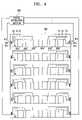
- FIG. 8 is a schematic view showing a mother substrate according to another exemplary embodiment of the present invention.
- a mother substrate 700 includes first, second, third, fourth, fifth and sixth areas A 1 , A 2 , A 3 , A 4 , A 5 and A 6 having an equal configuration to each other, and thus the first area A 1 will be described and a description of the second to sixth areas A 2 , A 3 , A 4 , A 5 and A 6 will be omitted.
- six-TFT areas formed at the first to sixth areas A 1 , A 2 , A 3 , A 4 , A 5 and A 6 , respectively, will be described.
- the first area A 1 includes first, second, third, fourth, fifth and sixth TFT areas 351 , 352 , 353 , 354 , 355 and 356 .
- First, second and third inspecting pad parts IP 1 , IP 2 and IP 3 are disposed at a left side of the first area A 1 so as to receive an inspection signal from a signal generating section 800 .
- the first, second and third inspecting pad parts IP 1 , IP 2 and IP 3 are electrically connected to the first, second and third TFT areas 351 , 352 and 353 through first, second and third inspection lines L 1 , L 2 and L 3 , respectively.
- the first, second and third inspection lines L 1 , L 2 and L 3 are electrically connected to inspection lines formed in the first, second and third TFT areas 351 , 352 and 353 .
- the first, second and third TFT areas 351 , 352 and 353 may be operated in response to the inspection signal, thereby inspecting the first, second and third TFT areas 351 , 352 and 353 formed on the mother substrate 700 .
- fourth, fifth and sixth inspecting pad parts IP 4 , IP 5 and IP 6 are disposed at a right side of the first area A 1 so as to receive the inspection signal from the signal generating section 800 .
- the fourth, fifth and sixth inspecting pad parts IP 4 , IP 5 and IP 6 are electrically connected to the fourth, fifth and sixth TFT areas 354 , 355 and 356 through fourth, fifth and sixth inspection lines L 4 , L 5 and L 6 , respectively.
- the fourth, fifth and sixth inspection lines L 4 , L 5 and L 6 are electrically connected to inspection lines formed in the fourth, fifth and sixth TFT areas 354 , 355 and 356 .
- the fourth, fifth and sixth TFT areas 354 , 355 and 356 may be operated in response to the inspection signal, thereby inspecting the fourth, fifth and sixth TFT areas 354 , 355 and 356 formed on the mother substrate 700 .
- FIG. 9 is a flowchart illustrating a method of manufacturing a display panel according to another exemplary embodiment of the present invention.
- FIG. 10A is a schematic view showing a mother substrate manufactured by the method shown in FIG. 9 .
- FIG. 10B is a schematic view showing a mother substrate for an upper substrate manufactured by the method shown in FIG. 9 .
- FIG. 10 is a schematic view showing an assembled substrate manufactured by the method shown in FIG. 9 .
- a mother substrate 700 on which a plurality of TFT areas is formed is completed (step S 10 ).
- the mother substrate 700 is inspected (step S 11 ).
- the inspection signal is applied to each of TFT areas through the first to sixth inspection lines L 1 , L 2 , L 3 , L 4 , L 5 and L 6 .
- a gate driving part GDP is driven to simultaneously output a driving signal to gate lines GL 1 –GLn.
- the TFT areas formed on the mother substrate 700 may be inspected.
- a mother substrate 500 for an upper substrate on which a plurality of color filter areas C/F is formed is completed (step S 12 ).
- the color filter areas C/F one-to-one correspond to the TFT areas.
- Each of the color filter areas C/F includes a color filter (not shown) having red (R), green (G) and blue (B) color pixels and a common electrode (not shown) used as a second electrode of a liquid crystal capacitor Clc (refer to FIG. 1 ).
- the common electrode is formed on the color filter.
- the completed mother substrate 700 for the lower substrate and the completed mother substrate 500 for the upper substrate are assembled to each other using a sealing member (hereinafter, referred to as sealant) 650 disposed between the completed mother substrate 700 for the lower substrate and the completed mother substrate 500 for the upper substrate, to thereby complete en assembled substrate 600 having a plurality of cello 610 (step 13 ).
- sealant a sealing member
- the assembled substrate 600 is cut such that the cells 610 are separated from each other, thereby completing an assembled substrate 300 far a display panel (step 14 ). Then, in step 515 , a visual inspection process is performed so as to inspect whether or not the assembled substrate 300 is operating normally.
- step S 16 an edge of the assembled substrate 300 for the display panel is grounded.
- the inspection line ISL formed on the assembled substrate 300 for the display panel, and the assembled substrate 300 for the display panel is completed as a display panel (step S 17 ).
- the lower substrate includes the inspection line that receives the first inspection signal, gate driving part electrically connected to me inspection line so as to output the second inspection signal in response to the first inspection signal, and pixel part driven in response to the second inspection signal.
- the pixel part may be easily inspected using the gate driving part while the display panel on which the gate driving part is formed is manufactured, or after the mother substrate and the substrate for the display panel are completed. Accordingly, the display panel may have an enhanced productivity and an improved yield.
Landscapes
- Engineering & Computer Science (AREA)
- Physics & Mathematics (AREA)
- General Physics & Mathematics (AREA)
- Computer Hardware Design (AREA)
- Theoretical Computer Science (AREA)
- Chemical & Material Sciences (AREA)
- Crystallography & Structural Chemistry (AREA)
- Nonlinear Science (AREA)
- Liquid Crystal (AREA)
- Optics & Photonics (AREA)
- Devices For Indicating Variable Information By Combining Individual Elements (AREA)
Priority Applications (2)
| Application Number | Priority Date | Filing Date | Title |
|---|---|---|---|
| US11/556,463 US7532025B2 (en) | 2003-07-14 | 2006-11-03 | Mother substrate, substrate for display panel and method of manufacturing display panel |
| US12/421,228 US7944228B2 (en) | 2003-07-14 | 2009-04-09 | Mother substrate, substrate for display panel and method of manufacturing display panel |
Applications Claiming Priority (2)
| Application Number | Priority Date | Filing Date | Title |
|---|---|---|---|
| KR1020030047723A KR100964620B1 (ko) | 2003-07-14 | 2003-07-14 | 하부기판용 모기판, 표시패널용 기판 및 표시패널의제조방법 |
| KR2003-47723 | 2003-07-14 |
Related Child Applications (1)
| Application Number | Title | Priority Date | Filing Date |
|---|---|---|---|
| US11/556,463 Continuation US7532025B2 (en) | 2003-07-14 | 2006-11-03 | Mother substrate, substrate for display panel and method of manufacturing display panel |
Publications (2)
| Publication Number | Publication Date |
|---|---|
| US20050012518A1 US20050012518A1 (en) | 2005-01-20 |
| US7145357B2 true US7145357B2 (en) | 2006-12-05 |
Family
ID=34056826
Family Applications (3)
| Application Number | Title | Priority Date | Filing Date |
|---|---|---|---|
| US10/777,990 Expired - Lifetime US7145357B2 (en) | 2003-07-14 | 2004-02-11 | Mother substrate, substrate for display panel and method of manufacturing display panel |
| US11/556,463 Expired - Lifetime US7532025B2 (en) | 2003-07-14 | 2006-11-03 | Mother substrate, substrate for display panel and method of manufacturing display panel |
| US12/421,228 Expired - Lifetime US7944228B2 (en) | 2003-07-14 | 2009-04-09 | Mother substrate, substrate for display panel and method of manufacturing display panel |
Family Applications After (2)
| Application Number | Title | Priority Date | Filing Date |
|---|---|---|---|
| US11/556,463 Expired - Lifetime US7532025B2 (en) | 2003-07-14 | 2006-11-03 | Mother substrate, substrate for display panel and method of manufacturing display panel |
| US12/421,228 Expired - Lifetime US7944228B2 (en) | 2003-07-14 | 2009-04-09 | Mother substrate, substrate for display panel and method of manufacturing display panel |
Country Status (5)
| Country | Link |
|---|---|
| US (3) | US7145357B2 (enExample) |
| JP (1) | JP4551146B2 (enExample) |
| KR (1) | KR100964620B1 (enExample) |
| CN (1) | CN100590480C (enExample) |
| TW (1) | TWI346207B (enExample) |
Cited By (6)
| Publication number | Priority date | Publication date | Assignee | Title |
|---|---|---|---|---|
| US20050078057A1 (en) * | 2003-08-19 | 2005-04-14 | Samsung Electronics Co., Ltd. | Display device, display panel therefor, and inspection method thereof |
| US20070057689A1 (en) * | 2003-07-14 | 2007-03-15 | Samsung Electronics Co., Ltd | Mother substrate, substrate for display panel and method of manufacturing display panel |
| US20080106288A1 (en) * | 2006-11-07 | 2008-05-08 | Apple Inc. | Circuit boards including removable test point portions and configurable testing platforms |
| US20100295829A1 (en) * | 2009-05-19 | 2010-11-25 | Samsung Electronics Co., Ltd. | Thin film transistor array panel and display device including the same |
| US8436636B2 (en) | 2006-10-10 | 2013-05-07 | Apple Inc. | Methods and apparatuses for testing circuit boards |
| US20140132876A1 (en) * | 2006-01-18 | 2014-05-15 | Samsung Display Co., Ltd. | Liquid crystal display |
Families Citing this family (16)
| Publication number | Priority date | Publication date | Assignee | Title |
|---|---|---|---|---|
| KR20060020651A (ko) * | 2003-06-04 | 2006-03-06 | 도시바 마쯔시따 디스플레이 테크놀로지 컴퍼니, 리미티드 | 어레이 기판의 검사 방법 |
| KR101217079B1 (ko) * | 2005-07-05 | 2012-12-31 | 삼성디스플레이 주식회사 | 표시장치 |
| KR20070120320A (ko) * | 2006-06-19 | 2007-12-24 | 엘지.필립스 엘시디 주식회사 | 액정표시장치 제조방법 및 이를 위한 대면적 기판 |
| KR101274922B1 (ko) * | 2006-06-26 | 2013-06-14 | 엘지디스플레이 주식회사 | 액정패널용 멀티 어레이 기판 |
| KR101346860B1 (ko) | 2006-06-29 | 2014-01-07 | 엘지디스플레이 주식회사 | 스크라이빙 장치 및 그를 이용한 액정패널 절단방법 |
| KR20080010837A (ko) * | 2006-07-28 | 2008-01-31 | 삼성전자주식회사 | 박막 트랜지스터 기판의 불량 검사 모듈 및 방법 |
| KR100749467B1 (ko) * | 2006-08-09 | 2007-08-14 | 삼성에스디아이 주식회사 | 유기발광표시장치 및 유기발광표시장치의 검사회로구동방법 |
| KR100749423B1 (ko) | 2006-08-09 | 2007-08-14 | 삼성에스디아이 주식회사 | 유기발광표시장치 및 유기발광표시장치의 검사회로구동방법 |
| KR100812023B1 (ko) * | 2006-08-23 | 2008-03-10 | 삼성에스디아이 주식회사 | 유기전계발광 표시장치 및 그 모기판 |
| KR100732819B1 (ko) * | 2006-08-30 | 2007-06-27 | 삼성에스디아이 주식회사 | 유기전계발광 표시장치 및 그의 모기판 |
| JP5445239B2 (ja) * | 2010-03-10 | 2014-03-19 | セイコーエプソン株式会社 | 電気光学装置及び電子機器 |
| US20130083457A1 (en) * | 2011-09-30 | 2013-04-04 | Apple Inc. | System and method for manufacturing a display panel or other patterned device |
| KR102231898B1 (ko) * | 2013-12-13 | 2021-03-25 | 엘지디스플레이 주식회사 | 표시장치 및 표시패널 |
| CN106526918B (zh) * | 2016-12-16 | 2019-05-28 | 惠科股份有限公司 | 一种显示基板及其测试方法 |
| CN109961729B (zh) * | 2019-04-30 | 2022-11-08 | 深圳市华星光电半导体显示技术有限公司 | 显示面板及其测试方法 |
| TWI756939B (zh) * | 2020-11-25 | 2022-03-01 | 友達光電股份有限公司 | 基板裝置、包含基板裝置之顯示面板及其製作方法 |
Citations (9)
| Publication number | Priority date | Publication date | Assignee | Title |
|---|---|---|---|---|
| US5148301A (en) * | 1990-02-27 | 1992-09-15 | Casio Computer Co., Ltd. | Liquid crystal display device having a driving circuit inside the seal boundary |
| US5576730A (en) * | 1992-04-08 | 1996-11-19 | Sharp Kabushiki Kaisha | Active matrix substrate and a method for producing the same |
| US5754158A (en) * | 1988-05-17 | 1998-05-19 | Seiko Epson Corporation | Liquid crystal device |
| US6411359B1 (en) * | 1998-04-24 | 2002-06-25 | Hitachi, Ltd. | Liquid crystal display device having smaller frame area |
| US20020084965A1 (en) * | 2000-12-30 | 2002-07-04 | Lg. Philips Lcd Co., Ltd. | Liquid crystal display device |
| US20030030464A1 (en) * | 2001-08-07 | 2003-02-13 | Kabushiki Kaisha Toshiba | Testing method for array substrate |
| US6750926B2 (en) * | 2000-03-06 | 2004-06-15 | Hitachi, Ltd. | Liquid crystal display device and manufacturing method thereof |
| US6781403B2 (en) * | 2001-12-20 | 2004-08-24 | Lg.Philips Lcd Co., Ltd. | Liquid crystal display panel for testing line on glass type signal lines |
| US6839121B2 (en) * | 2001-12-29 | 2005-01-04 | Lg. Philips Lcd Co., Ltd. | Liquid crystal display device formed on glass substrate having improved efficiency |
Family Cites Families (6)
| Publication number | Priority date | Publication date | Assignee | Title |
|---|---|---|---|---|
| JP2852063B2 (ja) * | 1989-04-10 | 1999-01-27 | 株式会社日立製作所 | 薄膜トランジスタ回路装置 |
| JPH055866A (ja) * | 1991-06-28 | 1993-01-14 | Sharp Corp | アクテイブマトリクス基板の検査方法 |
| JPH08190087A (ja) * | 1995-01-09 | 1996-07-23 | Hitachi Ltd | 液晶表示パネル作製用透明絶縁基板およびその各種特性検査方法 |
| JP2002009407A (ja) * | 2000-06-20 | 2002-01-11 | Sharp Corp | 配線基板 |
| JP2002229056A (ja) * | 2001-02-05 | 2002-08-14 | Toshiba Corp | 表示装置用電極基板及びその検査方法 |
| KR100964620B1 (ko) * | 2003-07-14 | 2010-06-22 | 삼성전자주식회사 | 하부기판용 모기판, 표시패널용 기판 및 표시패널의제조방법 |
-
2003
- 2003-07-14 KR KR1020030047723A patent/KR100964620B1/ko not_active Expired - Fee Related
-
2004
- 2004-02-11 US US10/777,990 patent/US7145357B2/en not_active Expired - Lifetime
- 2004-03-10 CN CN200410008429A patent/CN100590480C/zh not_active Expired - Lifetime
- 2004-04-13 TW TW093110268A patent/TWI346207B/zh not_active IP Right Cessation
- 2004-07-13 JP JP2004206356A patent/JP4551146B2/ja not_active Expired - Lifetime
-
2006
- 2006-11-03 US US11/556,463 patent/US7532025B2/en not_active Expired - Lifetime
-
2009
- 2009-04-09 US US12/421,228 patent/US7944228B2/en not_active Expired - Lifetime
Patent Citations (9)
| Publication number | Priority date | Publication date | Assignee | Title |
|---|---|---|---|---|
| US5754158A (en) * | 1988-05-17 | 1998-05-19 | Seiko Epson Corporation | Liquid crystal device |
| US5148301A (en) * | 1990-02-27 | 1992-09-15 | Casio Computer Co., Ltd. | Liquid crystal display device having a driving circuit inside the seal boundary |
| US5576730A (en) * | 1992-04-08 | 1996-11-19 | Sharp Kabushiki Kaisha | Active matrix substrate and a method for producing the same |
| US6411359B1 (en) * | 1998-04-24 | 2002-06-25 | Hitachi, Ltd. | Liquid crystal display device having smaller frame area |
| US6750926B2 (en) * | 2000-03-06 | 2004-06-15 | Hitachi, Ltd. | Liquid crystal display device and manufacturing method thereof |
| US20020084965A1 (en) * | 2000-12-30 | 2002-07-04 | Lg. Philips Lcd Co., Ltd. | Liquid crystal display device |
| US20030030464A1 (en) * | 2001-08-07 | 2003-02-13 | Kabushiki Kaisha Toshiba | Testing method for array substrate |
| US6781403B2 (en) * | 2001-12-20 | 2004-08-24 | Lg.Philips Lcd Co., Ltd. | Liquid crystal display panel for testing line on glass type signal lines |
| US6839121B2 (en) * | 2001-12-29 | 2005-01-04 | Lg. Philips Lcd Co., Ltd. | Liquid crystal display device formed on glass substrate having improved efficiency |
Cited By (18)
| Publication number | Priority date | Publication date | Assignee | Title |
|---|---|---|---|---|
| US7944228B2 (en) | 2003-07-14 | 2011-05-17 | Samsung Electronics Co., Ltd. | Mother substrate, substrate for display panel and method of manufacturing display panel |
| US20070057689A1 (en) * | 2003-07-14 | 2007-03-15 | Samsung Electronics Co., Ltd | Mother substrate, substrate for display panel and method of manufacturing display panel |
| US7532025B2 (en) * | 2003-07-14 | 2009-05-12 | Samsung Electronics Co., Ltd. | Mother substrate, substrate for display panel and method of manufacturing display panel |
| US20090195745A1 (en) * | 2003-07-14 | 2009-08-06 | Samsung Electronics Co., Ltd. | Mother substrate, substrate for display panel and method of manufacturing display panel |
| US20050078057A1 (en) * | 2003-08-19 | 2005-04-14 | Samsung Electronics Co., Ltd. | Display device, display panel therefor, and inspection method thereof |
| US7663395B2 (en) * | 2003-08-19 | 2010-02-16 | Samsung Electronics Co., Ltd. | Display device, display panel therefor, and inspection method thereof |
| US10690982B2 (en) | 2006-01-18 | 2020-06-23 | Samsung Display Co., Ltd. | Display device |
| US9606405B2 (en) * | 2006-01-18 | 2017-03-28 | Samsung Display Co., Ltd. | Liquid crystal display |
| US10261377B2 (en) * | 2006-01-18 | 2019-04-16 | Samsung Display Co., Ltd. | Liquid crystal display |
| US20170162160A1 (en) * | 2006-01-18 | 2017-06-08 | Samsung Display Co., Ltd. | Liquid crystal display |
| US20140132876A1 (en) * | 2006-01-18 | 2014-05-15 | Samsung Display Co., Ltd. | Liquid crystal display |
| US11237442B2 (en) | 2006-01-18 | 2022-02-01 | Samsung Display Co., Ltd. | Liquid crystal display |
| US8436636B2 (en) | 2006-10-10 | 2013-05-07 | Apple Inc. | Methods and apparatuses for testing circuit boards |
| US9513314B2 (en) | 2006-11-07 | 2016-12-06 | Apple Inc. | Configurable testing platforms for circuit boards with removable test point portions |
| US8362793B2 (en) * | 2006-11-07 | 2013-01-29 | Apple Inc. | Circuit boards including removable test point portions and configurable testing platforms |
| US20080106288A1 (en) * | 2006-11-07 | 2008-05-08 | Apple Inc. | Circuit boards including removable test point portions and configurable testing platforms |
| US8232984B2 (en) * | 2009-05-19 | 2012-07-31 | Samsung Electronics Co., Ltd. | Thin film transistor array panel having a driver inspection unit and display device including the same |
| US20100295829A1 (en) * | 2009-05-19 | 2010-11-25 | Samsung Electronics Co., Ltd. | Thin film transistor array panel and display device including the same |
Also Published As
| Publication number | Publication date |
|---|---|
| KR100964620B1 (ko) | 2010-06-22 |
| CN1576965A (zh) | 2005-02-09 |
| US20050012518A1 (en) | 2005-01-20 |
| TW200523861A (en) | 2005-07-16 |
| US20070057689A1 (en) | 2007-03-15 |
| US7532025B2 (en) | 2009-05-12 |
| KR20050008043A (ko) | 2005-01-21 |
| CN100590480C (zh) | 2010-02-17 |
| JP4551146B2 (ja) | 2010-09-22 |
| US20090195745A1 (en) | 2009-08-06 |
| JP2005037942A (ja) | 2005-02-10 |
| TWI346207B (en) | 2011-08-01 |
| US7944228B2 (en) | 2011-05-17 |
Similar Documents
| Publication | Publication Date | Title |
|---|---|---|
| US7944228B2 (en) | Mother substrate, substrate for display panel and method of manufacturing display panel | |
| US8223108B2 (en) | Array substrate and display apparatus having the same | |
| US8471981B2 (en) | Display apparatus and display set having the same | |
| US8194057B2 (en) | Display apparatus | |
| US7816683B2 (en) | Array substrate and display apparatus having the same | |
| US10777159B2 (en) | Gate driver and display apparatus having the same | |
| US20080180592A1 (en) | Liquid crystal display panel and testing system and method thereof | |
| US20130293800A1 (en) | Array substrate and a display apparatus having the same | |
| US9734785B2 (en) | Gate driving unit | |
| US20090262058A1 (en) | Display apparatus having reduced kickback voltage | |
| CN1982952A (zh) | 显示基板和测试该显示基板的方法 | |
| US8264250B2 (en) | Array substrate having increased inspection efficiency and display apparatus having the same | |
| KR20080070918A (ko) | 표시 패널의 불량 검사 모듈 및 방법 | |
| KR101604492B1 (ko) | 액정표시장치 | |
| US8305546B2 (en) | Mother substrate for liquid crystal display device and method of fabricating liquid crystal display device | |
| WO2016185642A1 (ja) | 表示パネル | |
| KR20080086126A (ko) | 액정표시장치와, 이의 검사공정을 포함하는 액정표시장치의제조방법 | |
| KR20070076843A (ko) | 박막 트랜지스터 기판 및 그 검사 방법 | |
| CN100538448C (zh) | 阵列基片及具有该阵列基片的显示器 | |
| KR100897503B1 (ko) | 액정표시장치 | |
| KR20060070196A (ko) | 어레이 기판 및 이를 갖는 표시장치 | |
| KR20070079679A (ko) | 표시 기판의 검사 방법 |
Legal Events
| Date | Code | Title | Description |
|---|---|---|---|
| AS | Assignment |
Owner name: SAMSUNG ELECTRONICS CO., LTD., KOREA, REPUBLIC OF Free format text: ASSIGNMENT OF ASSIGNORS INTEREST;ASSIGNOR:LEE, BACK-WON;REEL/FRAME:014997/0157 Effective date: 20031210 |
|
| STCF | Information on status: patent grant |
Free format text: PATENTED CASE |
|
| FPAY | Fee payment |
Year of fee payment: 4 |
|
| AS | Assignment |
Owner name: SAMSUNG DISPLAY CO., LTD., KOREA, REPUBLIC OF Free format text: ASSIGNMENT OF ASSIGNORS INTEREST;ASSIGNOR:SAMSUNG ELECTRONICS CO., LTD.;REEL/FRAME:028984/0774 Effective date: 20120904 |
|
| FEPP | Fee payment procedure |
Free format text: PAYOR NUMBER ASSIGNED (ORIGINAL EVENT CODE: ASPN); ENTITY STATUS OF PATENT OWNER: LARGE ENTITY |
|
| FPAY | Fee payment |
Year of fee payment: 8 |
|
| MAFP | Maintenance fee payment |
Free format text: PAYMENT OF MAINTENANCE FEE, 12TH YEAR, LARGE ENTITY (ORIGINAL EVENT CODE: M1553) Year of fee payment: 12 |