US7137687B2 - Liquid discharge head, liquid discharge apparatus, and method for forming liquid discharge head - Google Patents
Liquid discharge head, liquid discharge apparatus, and method for forming liquid discharge head Download PDFInfo
- Publication number
- US7137687B2 US7137687B2 US10/480,241 US48024103A US7137687B2 US 7137687 B2 US7137687 B2 US 7137687B2 US 48024103 A US48024103 A US 48024103A US 7137687 B2 US7137687 B2 US 7137687B2
- Authority
- US
- United States
- Prior art keywords
- liquid
- liquid discharge
- wall structures
- walls
- substrate
- Prior art date
- Legal status (The legal status is an assumption and is not a legal conclusion. Google has not performed a legal analysis and makes no representation as to the accuracy of the status listed.)
- Expired - Fee Related
Links
- 239000007788 liquid Substances 0.000 title claims abstract description 266
- 238000000034 method Methods 0.000 title description 60
- 229920001971 elastomer Polymers 0.000 claims abstract description 115
- 239000005060 rubber Substances 0.000 claims abstract description 115
- 239000000758 substrate Substances 0.000 claims abstract description 93
- 239000000463 material Substances 0.000 claims abstract description 60
- 239000000853 adhesive Substances 0.000 claims abstract description 38
- 230000001070 adhesive effect Effects 0.000 claims abstract description 38
- 239000013013 elastic material Substances 0.000 claims abstract description 27
- 239000000126 substance Substances 0.000 claims abstract description 14
- 239000011347 resin Substances 0.000 claims description 58
- 229920005989 resin Polymers 0.000 claims description 58
- 238000007639 printing Methods 0.000 claims description 43
- 230000004913 activation Effects 0.000 claims description 24
- 229920001195 polyisoprene Polymers 0.000 claims description 10
- 229920002857 polybutadiene Polymers 0.000 claims description 9
- 238000007599 discharging Methods 0.000 claims description 7
- 229920001721 polyimide Polymers 0.000 abstract description 74
- 239000004642 Polyimide Substances 0.000 abstract description 73
- 239000010410 layer Substances 0.000 description 45
- 239000000976 ink Substances 0.000 description 42
- 238000004519 manufacturing process Methods 0.000 description 34
- 238000012546 transfer Methods 0.000 description 30
- 230000007423 decrease Effects 0.000 description 27
- 239000004065 semiconductor Substances 0.000 description 24
- 230000008569 process Effects 0.000 description 22
- 238000000206 photolithography Methods 0.000 description 19
- 238000007650 screen-printing Methods 0.000 description 13
- 239000002904 solvent Substances 0.000 description 13
- PXHVJJICTQNCMI-UHFFFAOYSA-N Nickel Chemical compound [Ni] PXHVJJICTQNCMI-UHFFFAOYSA-N 0.000 description 12
- 230000007774 longterm Effects 0.000 description 12
- 230000000694 effects Effects 0.000 description 11
- 238000010894 electron beam technology Methods 0.000 description 11
- 238000012545 processing Methods 0.000 description 11
- 230000000994 depressogenic effect Effects 0.000 description 10
- 238000000059 patterning Methods 0.000 description 10
- 230000008961 swelling Effects 0.000 description 9
- 230000003628 erosive effect Effects 0.000 description 8
- 239000002243 precursor Substances 0.000 description 8
- 238000004528 spin coating Methods 0.000 description 8
- 239000003822 epoxy resin Substances 0.000 description 7
- 229920000647 polyepoxide Polymers 0.000 description 7
- 239000011248 coating agent Substances 0.000 description 6
- 238000000576 coating method Methods 0.000 description 6
- 229910052759 nickel Inorganic materials 0.000 description 6
- 238000004132 cross linking Methods 0.000 description 5
- 238000007766 curtain coating Methods 0.000 description 5
- 238000010017 direct printing Methods 0.000 description 5
- 238000010023 transfer printing Methods 0.000 description 5
- 206010034972 Photosensitivity reaction Diseases 0.000 description 4
- 238000007649 pad printing Methods 0.000 description 4
- 229920002120 photoresistant polymer Polymers 0.000 description 4
- 230000036211 photosensitivity Effects 0.000 description 4
- 239000005062 Polybutadiene Substances 0.000 description 3
- XUIMIQQOPSSXEZ-UHFFFAOYSA-N Silicon Chemical compound [Si] XUIMIQQOPSSXEZ-UHFFFAOYSA-N 0.000 description 3
- 230000008859 change Effects 0.000 description 3
- 238000005530 etching Methods 0.000 description 3
- 238000010438 heat treatment Methods 0.000 description 3
- 229910052710 silicon Inorganic materials 0.000 description 3
- 239000010703 silicon Substances 0.000 description 3
- 239000004925 Acrylic resin Substances 0.000 description 2
- 229920000178 Acrylic resin Polymers 0.000 description 2
- 239000012790 adhesive layer Substances 0.000 description 2
- 239000013043 chemical agent Substances 0.000 description 2
- 238000006243 chemical reaction Methods 0.000 description 2
- 239000003153 chemical reaction reagent Substances 0.000 description 2
- 239000003795 chemical substances by application Substances 0.000 description 2
- 150000001875 compounds Chemical class 0.000 description 2
- 238000011161 development Methods 0.000 description 2
- 239000000975 dye Substances 0.000 description 2
- 238000005516 engineering process Methods 0.000 description 2
- 150000002148 esters Chemical class 0.000 description 2
- 230000001678 irradiating effect Effects 0.000 description 2
- 239000002184 metal Substances 0.000 description 2
- 229910052751 metal Inorganic materials 0.000 description 2
- -1 methacryloyl groups Chemical group 0.000 description 2
- 239000000203 mixture Substances 0.000 description 2
- 238000007645 offset printing Methods 0.000 description 2
- 229920005575 poly(amic acid) Polymers 0.000 description 2
- 238000006116 polymerization reaction Methods 0.000 description 2
- LLHKCFNBLRBOGN-UHFFFAOYSA-N propylene glycol methyl ether acetate Chemical compound COCC(C)OC(C)=O LLHKCFNBLRBOGN-UHFFFAOYSA-N 0.000 description 2
- 239000011241 protective layer Substances 0.000 description 2
- 230000004044 response Effects 0.000 description 2
- 230000002441 reversible effect Effects 0.000 description 2
- 238000012360 testing method Methods 0.000 description 2
- MLIWQXBKMZNZNF-MZGHLJKDSA-N (2z,6z)-2,6-bis[(4-azidophenyl)methylidene]-4-methylcyclohexan-1-one Chemical compound O=C1\C(=C/C=2C=CC(=CC=2)N=[N+]=[N-])CC(C)C\C1=C\C1=CC=C(N=[N+]=[N-])C=C1 MLIWQXBKMZNZNF-MZGHLJKDSA-N 0.000 description 1
- IJGRMHOSHXDMSA-UHFFFAOYSA-N Atomic nitrogen Chemical compound N#N IJGRMHOSHXDMSA-UHFFFAOYSA-N 0.000 description 1
- 229920001342 Bakelite® Polymers 0.000 description 1
- 235000010724 Wisteria floribunda Nutrition 0.000 description 1
- 239000002253 acid Substances 0.000 description 1
- 230000003321 amplification Effects 0.000 description 1
- 238000003486 chemical etching Methods 0.000 description 1
- 229920003211 cis-1,4-polyisoprene Polymers 0.000 description 1
- 239000003086 colorant Substances 0.000 description 1
- 238000006356 dehydrogenation reaction Methods 0.000 description 1
- 230000006866 deterioration Effects 0.000 description 1
- BTTLGZVIWJDGCM-UHFFFAOYSA-N diazonio-[4-[[3-[(4-diazonioazanidylphenyl)methylidene]-5-oxocyclohexylidene]methyl]phenyl]azanide Chemical compound C1C(=O)CC(=CC=2C=CC([N-][N+]#N)=CC=2)CC1=CC1=CC=C([N-][N+]#N)C=C1 BTTLGZVIWJDGCM-UHFFFAOYSA-N 0.000 description 1
- 229910001873 dinitrogen Inorganic materials 0.000 description 1
- 238000005323 electroforming Methods 0.000 description 1
- 238000000866 electrolytic etching Methods 0.000 description 1
- 238000009713 electroplating Methods 0.000 description 1
- LNEPOXFFQSENCJ-UHFFFAOYSA-N haloperidol Chemical compound C1CC(O)(C=2C=CC(Cl)=CC=2)CCN1CCCC(=O)C1=CC=C(F)C=C1 LNEPOXFFQSENCJ-UHFFFAOYSA-N 0.000 description 1
- 239000012770 industrial material Substances 0.000 description 1
- 230000001788 irregular Effects 0.000 description 1
- 238000005304 joining Methods 0.000 description 1
- 230000007246 mechanism Effects 0.000 description 1
- 230000004048 modification Effects 0.000 description 1
- 238000012986 modification Methods 0.000 description 1
- 238000003199 nucleic acid amplification method Methods 0.000 description 1
- 239000002798 polar solvent Substances 0.000 description 1
- KOUKXHPPRFNWPP-UHFFFAOYSA-N pyrazine-2,5-dicarboxylic acid;hydrate Chemical compound O.OC(=O)C1=CN=C(C(O)=O)C=N1 KOUKXHPPRFNWPP-UHFFFAOYSA-N 0.000 description 1
- 230000035945 sensitivity Effects 0.000 description 1
- 238000004381 surface treatment Methods 0.000 description 1
Images


Classifications
-
- B—PERFORMING OPERATIONS; TRANSPORTING
- B41—PRINTING; LINING MACHINES; TYPEWRITERS; STAMPS
- B41J—TYPEWRITERS; SELECTIVE PRINTING MECHANISMS, i.e. MECHANISMS PRINTING OTHERWISE THAN FROM A FORME; CORRECTION OF TYPOGRAPHICAL ERRORS
- B41J2/00—Typewriters or selective printing mechanisms characterised by the printing or marking process for which they are designed
- B41J2/005—Typewriters or selective printing mechanisms characterised by the printing or marking process for which they are designed characterised by bringing liquid or particles selectively into contact with a printing material
- B41J2/01—Ink jet
- B41J2/015—Ink jet characterised by the jet generation process
- B41J2/04—Ink jet characterised by the jet generation process generating single droplets or particles on demand
- B41J2/045—Ink jet characterised by the jet generation process generating single droplets or particles on demand by pressure, e.g. electromechanical transducers
- B41J2/05—Ink jet characterised by the jet generation process generating single droplets or particles on demand by pressure, e.g. electromechanical transducers produced by the application of heat
-
- B—PERFORMING OPERATIONS; TRANSPORTING
- B41—PRINTING; LINING MACHINES; TYPEWRITERS; STAMPS
- B41J—TYPEWRITERS; SELECTIVE PRINTING MECHANISMS, i.e. MECHANISMS PRINTING OTHERWISE THAN FROM A FORME; CORRECTION OF TYPOGRAPHICAL ERRORS
- B41J2/00—Typewriters or selective printing mechanisms characterised by the printing or marking process for which they are designed
- B41J2/005—Typewriters or selective printing mechanisms characterised by the printing or marking process for which they are designed characterised by bringing liquid or particles selectively into contact with a printing material
- B41J2/01—Ink jet
- B41J2/135—Nozzles
- B41J2/14—Structure thereof only for on-demand ink jet heads
- B41J2/14016—Structure of bubble jet print heads
- B41J2/14032—Structure of the pressure chamber
- B41J2/1404—Geometrical characteristics
-
- B—PERFORMING OPERATIONS; TRANSPORTING
- B41—PRINTING; LINING MACHINES; TYPEWRITERS; STAMPS
- B41J—TYPEWRITERS; SELECTIVE PRINTING MECHANISMS, i.e. MECHANISMS PRINTING OTHERWISE THAN FROM A FORME; CORRECTION OF TYPOGRAPHICAL ERRORS
- B41J2/00—Typewriters or selective printing mechanisms characterised by the printing or marking process for which they are designed
- B41J2/005—Typewriters or selective printing mechanisms characterised by the printing or marking process for which they are designed characterised by bringing liquid or particles selectively into contact with a printing material
- B41J2/01—Ink jet
- B41J2/135—Nozzles
- B41J2/145—Arrangement thereof
- B41J2/15—Arrangement thereof for serial printing
-
- B—PERFORMING OPERATIONS; TRANSPORTING
- B41—PRINTING; LINING MACHINES; TYPEWRITERS; STAMPS
- B41J—TYPEWRITERS; SELECTIVE PRINTING MECHANISMS, i.e. MECHANISMS PRINTING OTHERWISE THAN FROM A FORME; CORRECTION OF TYPOGRAPHICAL ERRORS
- B41J2/00—Typewriters or selective printing mechanisms characterised by the printing or marking process for which they are designed
- B41J2/005—Typewriters or selective printing mechanisms characterised by the printing or marking process for which they are designed characterised by bringing liquid or particles selectively into contact with a printing material
- B41J2/01—Ink jet
- B41J2/135—Nozzles
- B41J2/16—Production of nozzles
- B41J2/1601—Production of bubble jet print heads
- B41J2/1603—Production of bubble jet print heads of the front shooter type
-
- B—PERFORMING OPERATIONS; TRANSPORTING
- B41—PRINTING; LINING MACHINES; TYPEWRITERS; STAMPS
- B41J—TYPEWRITERS; SELECTIVE PRINTING MECHANISMS, i.e. MECHANISMS PRINTING OTHERWISE THAN FROM A FORME; CORRECTION OF TYPOGRAPHICAL ERRORS
- B41J2/00—Typewriters or selective printing mechanisms characterised by the printing or marking process for which they are designed
- B41J2/005—Typewriters or selective printing mechanisms characterised by the printing or marking process for which they are designed characterised by bringing liquid or particles selectively into contact with a printing material
- B41J2/01—Ink jet
- B41J2/135—Nozzles
- B41J2/16—Production of nozzles
- B41J2/1621—Manufacturing processes
- B41J2/1631—Manufacturing processes photolithography
-
- B—PERFORMING OPERATIONS; TRANSPORTING
- B41—PRINTING; LINING MACHINES; TYPEWRITERS; STAMPS
- B41J—TYPEWRITERS; SELECTIVE PRINTING MECHANISMS, i.e. MECHANISMS PRINTING OTHERWISE THAN FROM A FORME; CORRECTION OF TYPOGRAPHICAL ERRORS
- B41J2/00—Typewriters or selective printing mechanisms characterised by the printing or marking process for which they are designed
- B41J2/005—Typewriters or selective printing mechanisms characterised by the printing or marking process for which they are designed characterised by bringing liquid or particles selectively into contact with a printing material
- B41J2/01—Ink jet
- B41J2/135—Nozzles
- B41J2/16—Production of nozzles
- B41J2/1621—Manufacturing processes
- B41J2/164—Manufacturing processes thin film formation
- B41J2/1645—Manufacturing processes thin film formation thin film formation by spincoating
-
- B—PERFORMING OPERATIONS; TRANSPORTING
- B41—PRINTING; LINING MACHINES; TYPEWRITERS; STAMPS
- B41J—TYPEWRITERS; SELECTIVE PRINTING MECHANISMS, i.e. MECHANISMS PRINTING OTHERWISE THAN FROM A FORME; CORRECTION OF TYPOGRAPHICAL ERRORS
- B41J2202/00—Embodiments of or processes related to ink-jet or thermal heads
- B41J2202/01—Embodiments of or processes related to ink-jet heads
- B41J2202/20—Modules
-
- Y—GENERAL TAGGING OF NEW TECHNOLOGICAL DEVELOPMENTS; GENERAL TAGGING OF CROSS-SECTIONAL TECHNOLOGIES SPANNING OVER SEVERAL SECTIONS OF THE IPC; TECHNICAL SUBJECTS COVERED BY FORMER USPC CROSS-REFERENCE ART COLLECTIONS [XRACs] AND DIGESTS
- Y10—TECHNICAL SUBJECTS COVERED BY FORMER USPC
- Y10T—TECHNICAL SUBJECTS COVERED BY FORMER US CLASSIFICATION
- Y10T29/00—Metal working
- Y10T29/49—Method of mechanical manufacture
- Y10T29/49002—Electrical device making
- Y10T29/49082—Resistor making
- Y10T29/49083—Heater type
-
- Y—GENERAL TAGGING OF NEW TECHNOLOGICAL DEVELOPMENTS; GENERAL TAGGING OF CROSS-SECTIONAL TECHNOLOGIES SPANNING OVER SEVERAL SECTIONS OF THE IPC; TECHNICAL SUBJECTS COVERED BY FORMER USPC CROSS-REFERENCE ART COLLECTIONS [XRACs] AND DIGESTS
- Y10—TECHNICAL SUBJECTS COVERED BY FORMER USPC
- Y10T—TECHNICAL SUBJECTS COVERED BY FORMER US CLASSIFICATION
- Y10T29/00—Metal working
- Y10T29/49—Method of mechanical manufacture
- Y10T29/49002—Electrical device making
- Y10T29/49117—Conductor or circuit manufacturing
- Y10T29/49124—On flat or curved insulated base, e.g., printed circuit, etc.
- Y10T29/4913—Assembling to base an electrical component, e.g., capacitor, etc.
-
- Y—GENERAL TAGGING OF NEW TECHNOLOGICAL DEVELOPMENTS; GENERAL TAGGING OF CROSS-SECTIONAL TECHNOLOGIES SPANNING OVER SEVERAL SECTIONS OF THE IPC; TECHNICAL SUBJECTS COVERED BY FORMER USPC CROSS-REFERENCE ART COLLECTIONS [XRACs] AND DIGESTS
- Y10—TECHNICAL SUBJECTS COVERED BY FORMER USPC
- Y10T—TECHNICAL SUBJECTS COVERED BY FORMER US CLASSIFICATION
- Y10T29/00—Metal working
- Y10T29/49—Method of mechanical manufacture
- Y10T29/49002—Electrical device making
- Y10T29/49117—Conductor or circuit manufacturing
- Y10T29/49124—On flat or curved insulated base, e.g., printed circuit, etc.
- Y10T29/49155—Manufacturing circuit on or in base
- Y10T29/49158—Manufacturing circuit on or in base with molding of insulated base
-
- Y—GENERAL TAGGING OF NEW TECHNOLOGICAL DEVELOPMENTS; GENERAL TAGGING OF CROSS-SECTIONAL TECHNOLOGIES SPANNING OVER SEVERAL SECTIONS OF THE IPC; TECHNICAL SUBJECTS COVERED BY FORMER USPC CROSS-REFERENCE ART COLLECTIONS [XRACs] AND DIGESTS
- Y10—TECHNICAL SUBJECTS COVERED BY FORMER USPC
- Y10T—TECHNICAL SUBJECTS COVERED BY FORMER US CLASSIFICATION
- Y10T29/00—Metal working
- Y10T29/49—Method of mechanical manufacture
- Y10T29/49002—Electrical device making
- Y10T29/49117—Conductor or circuit manufacturing
- Y10T29/49169—Assembling electrical component directly to terminal or elongated conductor
- Y10T29/49171—Assembling electrical component directly to terminal or elongated conductor with encapsulating
- Y10T29/49172—Assembling electrical component directly to terminal or elongated conductor with encapsulating by molding of insulating material
-
- Y—GENERAL TAGGING OF NEW TECHNOLOGICAL DEVELOPMENTS; GENERAL TAGGING OF CROSS-SECTIONAL TECHNOLOGIES SPANNING OVER SEVERAL SECTIONS OF THE IPC; TECHNICAL SUBJECTS COVERED BY FORMER USPC CROSS-REFERENCE ART COLLECTIONS [XRACs] AND DIGESTS
- Y10—TECHNICAL SUBJECTS COVERED BY FORMER USPC
- Y10T—TECHNICAL SUBJECTS COVERED BY FORMER US CLASSIFICATION
- Y10T29/00—Metal working
- Y10T29/49—Method of mechanical manufacture
- Y10T29/49401—Fluid pattern dispersing device making, e.g., ink jet
Definitions
- the present invention relates to a liquid discharge head, a liquid discharge apparatus, and a method for forming the liquid discharge head, and may be included in an inkjet printer.
- the present invention effectively prevents decrease in reliability with use by fixing a nozzle sheet on a substrate with a predetermined material that has an excellent chemical resistance and sufficient adhesiveness, or more specifically, by fixing the nozzle sheet on the substrate with cyclized rubber or with patternable, adhesive elastic material.
- the present invention may effectively prevent a decrease in reliability by forming walls for liquid chambers and liquid channels with polyimide.
- inkjet printers print desired images on printing stock, such as paper, by discharging ink droplets from a printer head onto the printing stock such as paper.
- the printer head included in the printer drives driving elements to change the pressure inside the liquid chambers so that the ink contained in the liquid chambers is discharged from nozzles as ink droplets.
- the driving elements may be heater elements or piezoelectric elements. Walls of the liquid chambers and the liquid channels are intricately formed with a resin such as epoxy resin or acrylic resin (Japanese Unexamined Patent Application Publication Nos. 61-154947, 62-253457, 3-184868, 6-286149, and 7-214783).
- the printer head is formed by, for example, a semiconductor manufacturing process, wherein, on the semiconductor substrate, driving circuits for driving the driving elements are simultaneously formed with the driving elements for changing the pressure inside the liquid chambers. Then, after a photosensitive epoxy resin is spin coated on the semiconductor substrate, the walls of the liquid chambers and the liquid channels are formed on the photosensitive epoxy resin by photolithography.
- a sheet including nozzles hereinafter referred as a ‘nozzle sheet’
- electrotyping is disposed on the semiconductor substrate.
- the nozzle sheet is thermocompressed to the photosensitive epoxy resin that forms the walls of the liquid chambers and the liquid channels.
- the resin such as epoxy resin forming the walls of the liquid chambers and the liquid channels erodes and swells with use. This erosion and swelling decreases the adhesive strength between the nozzle sheet and the end faces of the walls. Therefore, in the worst case, gaps form between the nozzle sheet and the end faces of the walls of neighboring liquid chambers, causing crosstalk between these liquid chambers.
- the adhesive strength between the nozzle sheet and the end faces of the walls is low from the beginning, causing even more gaps to form and worsening the crosstalk.
- the present invention provides a liquid discharge head, a liquid discharge apparatus and a method for forming a liquid discharge head that can effectively prevent a decrease in reliability with use.
- the present invention provides a liquid discharge head, wherein the pressure inside the liquid chambers is changed by driving elements and wherein droplets of liquid contained in the liquid chambers are discharged from predetermined nozzles.
- the driving elements are disposed on a substrate, which has walls forming the liquid chambers and the liquid channels for supplying liquid to the liquid chambers.
- a nozzle sheet which includes nozzles, is bonded. At least the bonding surfaces of the walls and the nozzle sheet should be chemically resistant to the liquid and may be formed with a predetermined material that sufficiently adheres to the nozzle sheet.
- the liquid discharge head has driving elements for changing the pressure inside the liquid chambers and discharges droplets of liquid contained in the liquid chambers from predetermined nozzles.
- the liquid discharge head may be applied to various devices such as the following: printer heads using liquids such as ink, various dyes, or liquid for forming protective layers; micro-dispensers, various measuring devices, and various test equipment using liquids such as reagents; or pattern-making devices using liquids such as chemical agents for etching protection.
- the driving elements are disposed on a substrate, which has walls forming liquid chambers and liquid channels for supplying liquid to the liquid chambers. On the walls of the liquid chambers and the liquid channels, the nozzle sheet with the nozzles is bonded. At least the bonding surface of the walls and the nozzle sheet should be chemically resistant to the liquid and should be formed with a predetermined material that sufficiently adheres to the nozzle sheet. As a result, a decrease in reliability with use is effectively prevented.
- the predetermined material may be cyclized rubber.
- the cyclized rubber used as the predetermined material for the liquid discharge head according to the present invention has an excellent chemical resistance and elasticity, is easily processed into intricate shapes by patterning, and has sufficient adhesiveness even when the nozzle sheet is formed of nickel. Consequently, the nozzle sheet may be attached firmly. Also, if the resin forming the walls swells, the portion to which the cyclized rubber is attached deforms. This deformation, however, may be absorbed, and, as a result, a decrease in reliability with long-term use is effectively prevented. The occurrence of crosstalk between neighboring liquid chambers is prevented during long-term use. When cyclized rubber is used for the printer head, high-resolution images may be printed.
- the nozzle sheet may be attached firmly. Also, if the resin forming the walls swells, the portion to which the cyclized rubber is attached deforms. This deformation, however, may be absorbed, and, as a result, a decrease in reliability with long-term use is effectively prevented. The occurrence of crosstalk between neighboring liquid chambers is prevented during the long-term use.
- cyclized rubber is used for a printer head, high-resolution images may be printed.
- the liquid discharge head according to the present invention has walls made of predetermined material formed on the substrate and the nozzle sheet is bonded to the end faces of these walls.
- the predetermined material may be polyimide.
- the liquid discharge head according to the present invention has, on the substrate, walls of the liquid chambers and the liquid channels for supplying liquid to the liquid chambers made of the predetermined material.
- the nozzle sheet is bonded onto the end faces of these walls. Since polyimide, which has excellent chemical resistance, is used as the predetermined material, swelling and erosion is prevented. As a result, a decrease in reliability with long-term use is effectively prevented. The occurrence of crosstalk between neighboring liquid chambers is also prevented during long-term use.
- polyimide When polyimide is used for the printer head, high-resolution images may be printed. Polyimide has sufficient adhesiveness and, thus, it has sufficient reliability. Polyimide, which is photosensitive, may be intricately processed by being irradiated with activation energy. Block-copolymerized polyimide easily exhibits various desired properties, and, consequently, it can be used with sufficient reliability for various types of processing such as printing.
- a liquid discharge apparatus includes a liquid discharge head for attaching droplets of liquid to printing stock.
- the liquid discharge head changes the pressure inside the liquid chambers with driving elements and discharges droplets of liquid contained in the liquid chambers from predetermined nozzles.
- the driving elements are disposed on a substrate, which has liquid chambers and liquid channels for supplying liquid to the liquid chambers.
- the nozzle sheet with the nozzles is bonded on the walls of the liquid chambers and liquid channels. At least the bonding surfaces of the walls and the nozzle sheet should be chemically resistant to the liquid and may be formed with a predetermined material that sufficiently adheres to the nozzle sheet.
- the predetermined material used in the liquid discharge head according to the present invention may be a patternable, adhesive elastic material.
- the liquid discharge apparatus has walls made of the predetermined material on the substrate and the nozzle sheet is bonded to the end faces of the walls.
- the predetermined material may be polyimide.
- the predetermined material for the method for forming the liquid discharge head according to the present invention may be cyclized rubber.
- the predetermined material for the method for forming the liquid discharge head according to the present invention may be a patternable, adhesive elastic material.
- the invention provides a liquid discharge apparatus that effectively prevents a decrease in reliability with long-term use.
- FIG. 1 is a perspective view of a printer head according to a first embodiment of the present invention.
- FIGS. 2(A) , 2 (B), 2 (C), 2 (D), and 2 (E) are perspective views of the manufacturing process of the printer head of FIG. 1 .
- FIG. 3 is a perspective view of a line printer using the printer head of FIG. 1 .
- FIG. 5 is a cross-sectional view describing the manufacturing process of a printer head according to a third embodiment of the present invention.
- FIGS. 6(A) , 6 (B), 6 (C), 6 (D), 6 (E), and 6 (F) are cross-sectional views describing the manufacturing process of a printer head according to a fourth embodiment of the present invention.
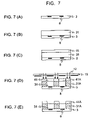
- FIGS. 7(A) , 7 (B), 7 (C), 7 (D), and 7 (E) are cross-sectional views describing the manufacturing process of a printer head according to a fifth embodiment of the present invention.
- FIGS. 8(F) , 8 (G), and 8 (H) are cross-sectional views describing the manufacturing process subsequent to FIG. 7(E) .
- FIGS. 9(A) , 9 (B), 9 (C), 9 (D), and 9 (E) are cross-sectional views describing the manufacturing process of a printer head according to a sixth embodiment of the present invention.
- FIGS. 10(F) , 10 (G), 10 (H), and 10 (I) are cross-sectional views describing the manufacturing process subsequent to FIG. 9(E) .
- FIG. 11 is a cross-sectional view describing the manufacturing process of a printer head according a seventh embodiment of the present invention.
- FIGS. 12(A) , 12 (B), 12 (C), 12 (D), 12 (E), and 12 (F) are cross-sectional views describing a printer head according to an eighth embodiment of the present invention.
- FIG. 1 is a perspective view including cross-sectional views of some portions of a printer head included in a printer according to a first embodiment of the present invention.
- the printer has a printer head 1 , which discharges ink droplets onto printing stock to print desired images.
- the printer head 1 is a printer head for a full line printer with a plurality of nozzles 2 arranged over the width of paper, which is the printing stock.
- the nozzles 2 are arranged in a line over the width of the paper.
- Each line of nozzles is predetermined to a particular color of ink. As a result, the printer head 1 can print color images.
- FIG. 1 is a perspective view showing a portion of the line of nozzles on the printer head 1 .
- the printer head 1 includes, on a substrate 3 , walls 5 of liquid chambers 4 containing ink, walls 6 of a liquid channel for supplying ink into the liquid chambers 4 , and a nozzle sheet 7 formed on these walls.
- the substrate 3 is formed by a semiconductor manufacturing process, wherein heater elements 8 , which are driving elements for changing the pressure inside the liquid chambers 4 , and driving circuits for driving these heater elements 8 are simultaneously formed on a silicon wafer.
- the wafer is divided into substrates 3 , having predetermined shapes. Consequently, the printer head 1 changes the pressure inside the liquid chambers 4 by the heater elements 8 , which are driving elements for changing the pressure inside the liquid chambers 4 , and discharges droplets of ink contained in the liquid chambers 4 from the nozzles 2 onto printing stock.
- the nozzle sheet 7 is a nickel sheet, which is formed by electrotyping, or a polyimide sheet with heat resistance.
- the nickel nozzle sheet 7 formed by electrotyping allows the fine nozzles 2 to be easily formed with high precision.
- the polyimide nozzle sheet 7 has excellent chemical resistance, providing high reliability.
- the walls 5 and 6 are entirely formed of patternable, adhesive elastic material.
- the nozzle sheet 7 is attached onto the substrate 3 with this patternable, adhesive elastic material. As a result, a decrease in reliability with use is effectively prevented.
- the walls 5 and 6 are formed with polyisoprene rubber, which is cyclized rubber.
- polyisoprene rubber is partly cyclized natural or synthetic cis-1,4-polyisoprene and has characteristics such as strong adhesiveness, stable quality, and high chemical resistance.
- Cyclized rubber is a photosensitive resist.
- the cyclized rubber which is a photosensitive resist, is a highly reliable material with a long history of being used as a rubber resist. Further, cyclized rubber is a highly polymerized compound including unsaturated double bonds in the molecule and is a material widely used for photofabrication.
- photofabrication is a generic term for the technology used for manufacturing various precision components by applying an electroforming technique or a combination of these techniques mainly based on techniques such as chemical etching, electrolytic etching, or electroplating, which uses, as masks, resist films patterned by photolithography techniques. Photofabrication is currently the mainstream technology for precision processing. In this embodiment, cyclized rubber is patterned by photolithography, and the walls 5 and 6 are intricately formed with high precision.
- cyclized rubber that is a photosensitive resist rubber resists made of polyisoprene or polybutadiene may be used. More specifically, Fuji Film Arch's SC Series, IC-T3 Series, HR Series, HNR Series, or VHR-2, Tokyo Ohka Kogyo's EPPR Series, or Zeon Corporation's ZPN103-39 may be used.
- FIGS. 2(A) to 2(E) are cross-sectional views describing the manufacturing process of the printer head 1 .
- the heater elements 8 are formed on the silicon substrate 3 by a semiconductor manufacturing process ( FIG. 2(A) ).
- the surface of the substrate 3 is treated or modified as required.
- a material layer is disposed on the substrate 3 to improve the adhesive strength between the substrate 3 and the walls 5 and 6 .
- the material layer disposed to improve the adhesive strength should be made of a material extensively used for this type of processing.
- a resist made of photosensitive cyclized rubber is applied onto the substrate 3 with a predetermined thickness, forming a resist layer 11 .
- various application methods used in semiconductor manufacturing processing such as spin coating, bar coating, or curtain coating may be used.
- the thickness of the resist layer 11 is arranged so that the final height of the liquid chambers 4 becomes the desired value.
- the resist layer 11 made of photosensitive cyclized rubber is selectively exposed to activation energy 12 .
- the exposed area is indicated by reference number 11 A.
- the activation energy 12 may be ultraviolet rays, electron beams, or X-rays, depending on the property of the resist.
- ultraviolet rays exposure equipment is used to irradiate the resist layer 11 made of cyclized rubber photosensitive to 280 [nm] to 480 [nm] with ultraviolet rays.
- reference number 13 indicates a photomask.
- the resist layer 11 is developed using specific liquid developers and solvents. Then the unexposed areas are removed from the resist layer 11 .
- photolithography using the activation energy 12 and walls 5 and 6 of the liquid chambers 4 the liquid channels are patterned onto the cyclized rubber.
- the nozzle sheet 7 is positioned and pressure-fixed.
- the nozzle sheet 7 is held by the adhesiveness of the patterned material (hereinafter referred to as ‘secondary adhesiveness’).
- the nozzle sheet 7 may simply be pressed to be bonded.
- its adhesive strength may be strengthened by supplying energy such as heat, light, or an electron beam. The energy such as heat, light, or an electron beam may be supplied while the nozzle sheet 7 is pressed.
- the cyclized rubber 11 A forming the walls 5 and 6 fixes the nozzle sheet 7 to the substrate 3 . Then the cyclized rubber 11 A is cured by baking to form a strong rubber film on cyclized rubber 11 B. Curing of the cyclized rubber 11 A may be performed before or while attaching the nozzle sheet 7 . When curing is performed before attaching the nozzle sheet 7 , it is necessary to make sure that the cyclized rubber has enough adhesive strength to attach the nozzle sheet 7 .
- FIG. 3 is a perspective view of a line printer having the printer head 1 .
- a line printer 101 is fully contained in a rectangular chassis 102 .
- a paper tray 103 containing paper 104 which is the recording medium, is inserted from a tray inlet formed on the front of the chassis 102 , allowing the paper 104 to be fed.
- the paper tray 103 is installed into the line printer 101 from the tray inlet. Then a mechanism pushes the paper 104 against a paper-feeding roller 106 . The rotation of the paper-feeding roller 106 causes the paper 104 to be pulled out from the paper tray 103 towards the back of the line printer 101 , as indicated by arrow A. On the back of the line printer 101 , reverse rollers 107 are disposed. The rotation of the reverse rollers 107 causes the paper 104 to be fed in the directions towards the front of the line printer 101 , as indicated by arrow B.
- the paper 104 fed in the direction indicated by arrow B passes over the paper tray 103 via spurring rollers 108 , as indicated by arrow C. Finally the paper 104 is ejected out from an outlet disposed on the front of the line printer 101 .
- a head cartridge 120 is disposed between the spurring rollers 108 and the outlet on the line printer 101 of the line printer 101 , as indicated by arrow D, so that it can be replaced when necessary.
- the head cartridge 120 includes the printer head 1 , which has yellow, magenta, cyan, and black line heads and which is disposed below a holder 122 formed in a particular shape.
- Ink cartridges Y, M, C, and B, for yellow, magenta, cyan, and black inks, respectively, are disposed on the holder 122 in the order. Consequently, the line printer 101 can print color images by discharging each color ink from the respective line head onto the paper 104 .
- the nozzle sheet forms a unit for the four colors. As a result, each discharge nozzle is positioned accurately and the cartridge can be easily replaced.
- FIG. 4 describes the arrangement of head chips 3 according to this embodiment.
- FIG. 4 is a partially enlarged drawing of FIG. 3 from the side of the paper 104 .
- identical head chips 3 are alternately (in a zigzag pattern) disposed on the nozzle sheet 7 , on both sides of ink channel 133 for each color ink.
- Each head chip 3 is disposed so that the heater elements 8 are located on the ink channel side.
- the head chips 3 on one side of the ink channel 133 are arranged so that they are rotated by 180° with respect to the head chips 3 on the opposite side of the ink channel 133 .
- ink may be supplied to each head chip 3 via one ink channel 133 system.
- high resolution may be achieved for the printing using a simple structure.
- Each of the pads 134 are disposed approximately in the middle of the head chips 3 , in the direction the nozzles 2 are aligned (the direction perpendicular to the direction of the paper is fed), and are rotated by 180° C. relative to each other so that the distance between each pad 134 becomes equal. Consequently, flexible wiring boards connected to the pads 134 of the neighboring head chips 3 of the printer head 1 are prevented from being too close to each other. In other words, the flexible wiring boards are prevented from being concentrated in one region.
- the driving sequence, in response to a driving signal, of the group of heaters 8 on the head chips 3 disposed on the upper side of the ink channel 133 is reversed with respect to the groups of heaters 8 on the lower side.
- the driving sequence of heaters 8 for each of the head chips 3 may be switched to a driving sequence corresponding to the heaters 8 disposed on the head chips 3 on each side of the channel 133 .
- the walls 5 of the liquid chambers 4 and the walls 6 of the liquid channels are formed of cyclized rubber, which is a patternable, adhesive elastic material.
- the nozzle sheet 7 is pressed and held against the walls 5 and 6 . In this way, on the printer head 1 , the nozzle sheet 7 is fixed to the substrate 3 with cyclized rubber, which is a patternable, adhesive elastic material.
- ink is supplied to the liquid chambers 4 through the liquid channels.
- the pressure inside the liquid chambers 4 is changed by driving the heater elements 8 . Due to the change in pressure, ink droplets are discharged from the nozzles 2 of the nozzle sheet 7 .
- the printer operates to attach the ink droplets discharged from the nozzles 2 to the printing stock.
- This embodiment uses cyclized rubber, which is a patternable, adhesive elastic material, for forming the walls 5 and 6 of the liquid chambers 4 and the liquid channels.
- cyclized rubber which is a patternable, adhesive elastic material, for forming the walls 5 and 6 of the liquid chambers 4 and the liquid channels.
- the walls 5 and 6 of the liquid chambers 4 and the liquid channels are formed of cyclized rubber, which is a patternable, adhesive elastic material.
- cyclized rubber which is a patternable, adhesive elastic material.
- the liquid chambers 4 and liquid channels may be formed with high precision by applying various micro fabrication techniques. As a result, deterioration of printing precision due to the difference in the fabrication of each liquid chamber 4 and liquid channel may be reduced and the difference in the quality of each finished product will thus be small.
- the liquid chambers 4 and the liquid channels may be formed with high precision by photolithography, which is a type of micro fabrication technique.
- photolithography which is a type of micro fabrication technique.
- the entire process from forming the silicon substrate 3 to forming the liquid chambers 4 and the liquid channels may be carried out by semiconductor manufacturing processes. As a result, sufficient reliability of the printer head may be acquired through a simple manufacturing process.
- the walls 5 and 6 of the liquid chambers 4 and the liquid channels are formed of cyclized rubber, which is a patternable, adhesive elastic material.
- the nozzle sheet 7 is pressed and held against these walls 5 and 6 . Consequently, by fixing the nozzle sheet 7 to the substrate 3 with cyclized rubber, which is a patternable, adhesive elastic material, a decrease in reliability with use is effectively prevented.
- the cyclized rubber is polyisoprene rubber, sufficient reliability may be acquired. Furthermore, sufficient reliability may be acquired for the photosensitive resist, which is subjected to photolithography.
- the photosensitivity of the cyclized rubber easily enables the walls of the liquid chambers and the liquid channels to be intricately formed with high precision by photolithography.
- the liquid chambers may be intricately formed with high precision by applying a semiconductor manufacturing process.
- This embodiment is the same as the first embodiment except that, instead of using polyisoprene rubber as the cyclized rubber, polybutadiene rubber is used.
- polybutadiene rubber Similar to polyisoprene rubber, which is cyclized rubber, polybutadiene rubber has a strong adhesive strength, stable properties, and a high chemical resistance. Moreover, polybutadiene rubber is a patternable, elastic material that is suitable for micro fabrication. Polybutadiene rubber may be used as a photosensitive resist by adding bis-azide compounds as a photosensitive group. In this embodiment, photosensitive cyclized rubber is used to form walls 5 and 6 of liquid chambers 4 and liquid channels by photolithography. A nozzle sheet 7 is pressure-fixed to the walls formed of photosensitive cyclized rubber.
- a bis-azide compound which is a photosensitive group of polybutadiene, becomes a nitrene radical by evolving nitrogen gas when irradiated with ultraviolet rays. Then the double bonds of the cyclized rubber undergo a crosslinking reaction, i.e. H-abstraction, and bonding reactions between the nitrene radicals occur, causing the portions exposed to ultraviolet rays to be selectively made insoluble in liquid developer.
- the exposure wavelength of bis-azide compounds is about 230 to 480 [nm].
- 2,6-di(4′-azidobenzylidene)-4-cyclohexanone and 2,6-di(4′-azidobenzylidene)-4-methylcyclohexanone have high response speed and are widely used materials.
- the same effects as the first embodiment may be acquired even if polybutadiene is used as the cyclized rubber instead of polyisoprene rubber, which is used in the first embodiment.
- walls of liquid chambers and liquid channels are formed with cyclized rubber by applying screen printing, which is a type of patterning and printing technique.
- cyclized rubber 16 in the formed of a resist paste, is disposed on a screen 15 , which is patterned in the same way as the shape of the walls.
- a squeegee 17 By moving a squeegee 17 , the cyclized rubber 16 is applied in the shape of the walls of the liquid chambers and liquid channels.
- processing such as baking is performed, if required, and the walls are formed by crosslinking.
- the mesh for the screen 15 is selected depending on the precision of the walls. Furthermore, the positioning and gap between the screen 15 and the substrate 3 , the tilt and the pressure of the squeegee 17 , and the viscosity of the cyclized rubber 16 are optimized.
- a nozzle sheet 7 is pressure-fixed, in the same way as described in the first embodiment, onto the walls formed as described above.
- the walls of the liquid chamber and the liquid channels may be formed even more efficiently.
- the intaglio 21 is pressed against a transfer pad 22 . Then, as shown in FIG. 6(C) , the transfer pad 22 is pulled apart from the intaglio 21 at a predetermined rate. As a result, the cyclized rubber 16 filled in the depressed portions of the intaglio 21 is transferred to the transfer pad 22 .
- the transfer pad 22 After moving the transfer pad 22 over a substrate 3 , the transfer pad 22 is pressed onto the substrate 3 , as shown in FIG. 6(D) . Then, as shown in FIG. 6(E) , by pulling the transfer pad 22 apart from the substrate 3 , the cyclized rubber 16 , which is shaped according to the shape of the walls on the transfer pad 22 , is transferred onto the substrate 3 . After letting the solvent of the cyclized rubber 16 dry, processing such as baking is performed, if required, and the walls 5 and 6 are formed by crosslinking. In this process, instead of moving the transfer pad 22 , the intaglio 21 and the substrate 3 may be moved. Each condition is optimized to position the intaglio 21 , the transfer pad 22 , and the substrate 3 , according to the required precision.
- a nozzle sheet 7 is pressure-fixed as described in the first embodiment.
- walls of liquid chambers and liquid channels are formed by alternately stacking cyclized rubber and a predetermined resin.
- a nozzle sheet is fixed to a substrate with cyclized rubber, which is a patternable, adhesive elastic material.
- the walls of the liquid chambers and the liquid channels are formed with photosensitive resin by photolithography, wherein the cyclized rubber and the resin are simultaneously patterned.
- the elastic material is patternable, intricate ink chambers and channels may be formed with high precision.
- the resin is photosensitive, after forming the bottom half of the walls by a semiconductor manufacturing process, the upper halves of the walls may be formed by stacking cyclized rubber on the bottom halves of the walls by various methods. By forming the walls of the liquid chambers and the liquid channels by simultaneously patterning the cyclized rubber and resin by photolithography using activation energy, walls with alternately stacked layers may be efficiently formed.
- FIGS. 7(A) to 8(H) are cross-sectional drawings describing the manufacturing processes of a printer head according to this embodiment. As shown in FIG. 7(A) , similar to the first embodiment, driving elements 8 and other parts are formed on a substrate 3 . Further, if required, the surface is treated and modified.
- a photosensitive resin 31 which forms the bottom halves of the walls, is applied onto the substrate 3 with a predetermined thickness.
- various application methods used in semiconductor manufacturing processes such as spin coating, bar coating, or curtain coating may be used.
- photosensitive epoxy resin and its derivatives, photosensitive acrylic resin and its derivatives, or photosensitive polyimide and its derivatives are suitable.
- the resin is not limited to the resins mentioned above, however, as long as the resin does not swell or erode due to the ink. Then, depending on the resin, the solvent is allowed to dry and the substrate 3 is heated to stabilize the resin film.
- a resist layer 41 is formed with photosensitive cyclized rubber by spin coating, bar coating, or curtain coating. Then, if required, the layer is dried or heated.
- the activation energy 12 may be ultraviolet rays, an electron beams, or X-rays, which are all used for photolithography.
- ultraviolet ray exposure equipment is used to irradiate the resist film 31 and the resist layer 41 , which are photosensitive to 280 [nm] to 480 [nm].
- the unexposed areas of the resist layer 41 are removed by developing the resist layer 41 using a developer or solvent.
- the tips 41 A of the walls 5 and 6 are formed by patterning cyclized rubber by photolithography using activation energy.
- the substrate 3 is washed by spin coating using a rinse agent 42 .
- the unexposed areas of the resist layer 31 are removed by developing the resist layer 31 using a developer or solvent. As a result, the walls 5 and 6 are formed.
- the layers 31 and 41 may be developed together at once by using a polar solvent such as propyleneglycol monomethyl ether acetate (PGMEA).
- a polar solvent such as propyleneglycol monomethyl ether acetate (PGMEA).
- PMEA propyleneglycol monomethyl ether acetate
- the nozzle sheet 7 is positioned and fixed by the adhesiveness of the patterned material forming the liquid channels.
- the sheet may be pressed and bonded, or the adhesiveness of the sheet may be improved by supplying energy such as heat, light, or an electron beam to the bonded nozzle sheet.
- the nozzle sheet 7 may be pressed against the walls while energy such as heat, light, or and an electron beam is supplied.
- the same effect as described in the first embodiment may be acquired. Since an appropriate resin can be selected, the degree of freedom of the selected material is improved.
- the bottom halves of the walls may be formed by patterning the resin by photolithography using activation energy.
- the cyclized rubber and resin are patterned simultaneously by photolithography using activation energy to form the walls of the liquid chambers and the liquid channels. In this way, even though the walls are formed by stacking layers, the walls may be formed by a semiconductor manufacturing process.
- the cyclized rubber and resin After simultaneously exposing the cyclized rubber and resin, the cyclized rubber and resin are developed individually or integrally. In this way, patterning suitable for the resin may be performed as required.
- driving elements and others are formed on the substrate and, then, as required, surface treatment and surface modification are performed.
- photosensitive resin 31 which forms the bottom halves of the walls, is applied onto the substrate 3 with a predetermined thickness.
- the walls are masked in the shape of the bottom halves of the walls with a photo mask 13 A, and the resist film 31 is irradiated with activation energy.
- the activation energy 12 may be ultraviolet rays, electron beams, or X-rays, which are all used for photolithography.
- post-exposure baking PEB
- Post-exposure baking may be performed during the exposure process or may be performed during any suitable process described later.
- the substrate 3 may be heated.
- the resist layer 41 made up of photosensitive cyclized rubber is formed by various application methods such as spin coating, bar coating, or curtain coating may be used and then, if required, dried and heated.
- the resist layer 41 is exposed while using the photo mask 13 B.
- any suitable type of activation energy 12 may be selected.
- the photo mask 13 B may have the same pattern as the photo mask 13 A used for exposing the film of resin 41 , or the photo mask 13 B may have a smaller width compared to the width of the photo mask 13 A.
- the resist layer 41 is developed using specific liquid developers and solvents. Then the unexposed areas are removed from the resist layer 11 . By patterning the cyclized rubber by photolithography using activation energy 12 , the tips 41 A of the walls 5 and 6 are formed.
- the nozzle sheet 7 is positioned and pressure-fixed. In this way, the nozzle sheet 7 is fixed by the adhesiveness of the patterned material forming the liquid channels.
- the sheet may be pressed and bonded, or the adhesiveness of the sheet may be improved by supplying energy such as heat, light, or an electron beam to the bonded nozzle sheet.
- the nozzle sheet 7 may be pressed against the walls while energy such as heat, light, or an electron beam may be supplied.
- the same effect as described in the first embodiment may be acquired. Since each layer is exposed individually, any appropriate resin can be selected, and, thus, the degree of freedom of the selected material is improved.
- the walls 5 and 6 of the liquid chambers 4 and the liquid channels are formed on the substrate 3 with a predetermined resin in the same manner as in a known process.
- a predetermined resin for the resin, an appropriate resin may be selected from the resins mentioned in the fifth embodiment.
- the walls of the liquid chambers and the liquid channels are formed by alternately stacking cyclized rubber and a predetermined resin
- the cyclized rubber may be stacked by screen printing. In this way, the same effect as in the first embodiment may be acquired.
- the cyclized rubber By stacking the cyclized rubber by screen printing, the cyclized rubber may be stacked after the walls are formed by known processes. Consequently, the reliability of the printer head may be improved by merely adding the screen printing process to the known processes.
- cyclized rubber is stacked by intaglio printing instead of screen printing.
- FIGS. 12(A) to 12(F) which are comparable to FIGS. 6(A) to 6(F) , walls 5 and 6 of liquid chambers and liquid channels are formed on a substrate 3 with a predetermined resin in a similar manner as in the seventh embodiment.
- a paste of cyclized rubber 16 is applied on an intaglio 21 , which is formed by the depressed portions of walls formed by the above processes.
- a squeegee 17 is moved to fill these depressed portions of the intaglio 21 with the cyclized rubber 16 and the excess cyclized rubber 16 is scraped off.
- a transfer pad 22 is pressed against the intaglio 21 . Then, as shown in FIG. 12(C) , the transfer pad 22 is pulled apart from the intaglio 21 at a predetermined rate. As a result, the cyclized rubber 16 filled in the depressed portions of the intaglio 21 is transferred to the transfer pad 22 .
- the transfer pad 22 After moving the transfer pad 22 onto the above substrate 3 , the transfer pad 22 is pressed onto the substrate 3 , as shown in FIG. 12(D) . Then, as shown in FIG. 12(E) , by pulling the transfer pad 22 apart from the substrate 3 , the cyclized rubber 16 fixed onto the transfer pad 22 is transferred onto the end faces of walls 5 A of the substrate 3 . After letting the solvent of the cyclized rubber 16 dry, processing such as baking is performed and the walls 5 and 6 are formed by crosslinking. In this process, instead of moving the transfer pad 22 , the intaglio 21 and the substrate 3 may be moved. According to the required precision, each condition is optimized to position the intaglio 21 , the transfer pad 22 , and the substrate 3 .
- a nozzle sheet 7 is pressure-fixed as described in the first embodiment.
- walls 5 and 6 are formed with polyimide.
- This embodiment is the same as the first embodiment except for the structures of the walls 5 and 6 . Therefore FIGS. 1 and 2(A) to 2 (E) are used for the description.
- a substrate 3 is formed by semiconductor manufacturing processes, wherein heater elements 8 , which are driving elements for changing the pressure inside the liquid chambers 4 , and driving circuits for driving these heater elements 8 are simultaneously formed on a semiconductor wafer.
- the wafer is divided into substrates 3 , having predetermined shapes. Consequently, at the printer head 1 the pressure inside the liquid chambers 4 is changed by the heater elements 8 , which are driving elements, and droplets of ink contained in the liquid chambers 4 are discharged from the nozzles 2 onto printing stock.
- the nozzle sheet 7 is a nickel sheet, which is formed by electrotyping, or a polyimide sheet with heat resistance.
- the nickel nozzle sheet 7 formed by electrotyping allows the fine nozzles 2 to be easily formed with high precision.
- the polyimide nozzle sheet 7 has excellent chemical resistance, providing high reliability.
- the walls 5 and 6 are entirely formed of polyimide to efficiently prevent a decrease in reliability with use.
- the polyimide is a block-copolymerized polyimide, which is a photoresist having sufficient adhesiveness. In this way, the walls can be formed easily by semiconductor manufacturing processes while maintaining sufficient adhesive strength.
- the block-copolymerized polyimide unlike known photosensitive polyimide, is directly synthesized into polyimide without going through the stage of polyamic acid, which is a polyimide precursor (U.S. Pat. No. 5,502,143 etc.) and which is generated by joining polymerized polyimide units (which are called a block).
- the block-copolymerized polyimide with desired properties may be freely designed and synthesized by configuring the properties of blocks, which are minimum units. Since the block units of the block-copolymerized polyimide have already undergone polyimidization, high temperature curing, which is necessary for known photosensitive polyimide, is unnecessary. In particular, for this embodiment, desired properties for the block-copolymerized polyimide are acquired by configuring each block.
- the surface of the substrate 3 is treated and modified if required. Then, a material layer for improving the adhesiveness between the substrate 3 and the walls 5 and 6 is formed on the substrate 3 .
- various materials that are used for this type of processing may be used.
- a photoresist made of block-copolymerized polyimide is applied onto the substrate 3 with a predetermined thickness to form a resist layer 11 .
- various application methods used in semiconductor manufacturing processing such as spin coating, bar coating, or curtain coating may be used.
- the thickness of the resist layer 11 is arranged so that the final height of the liquid chambers 4 becomes the desired value.
- the resist layer 11 is selectively exposed to activation energy 12 to bond each block in the resist.
- the exposed area is indicated by reference number 11 A.
- the activation energy 12 may be ultraviolet rays, electron beams, or X-rays, depending on the properties of the resist.
- the resist layer 11 is irradiated with ultraviolet rays.
- reference number 13 indicates a photo mask.
- the resist layer 11 is developed using specific liquid developers and solvents. Then the unexposed areas are removed from the resist layer 11 .
- the walls 5 and 6 of the liquid chambers 4 and the liquid channels are patterned and formed with polyimide.
- the nozzle sheet 7 is positioned and pressure-fixed.
- the nozzle sheet 7 is fixed by the adhesiveness of the patterned material.
- the adhesiveness may be strengthened by supplying energy such as heat, light, or an electron beam while the nozzle sheet 7 is being pressure-fixed to the walls.
- a positive type photoresist made of block-copolymerized polyimide may also be used.
- the processes applied are the same as the above negative type photoresist except that the pattern of the photo mask used for exposure and the processing of the unexposed portions differ.
- the printer head 1 includes the semiconductor substrate 3 , which has driving elements and other parts. On the semiconductor substrate 3 , the walls 5 and 6 of the liquid chambers 4 and the liquid channels are formed with polyimide. The nozzle sheet 7 is pressed and held against the end faces of the walls 5 and 6 . For the printer head 1 that is formed in this way, ink is supplied to the liquid chambers 4 through the liquid channels. The pressure inside the liquid chambers 4 is changed by driving the heater elements 8 . Due to the change in pressure, ink droplets are discharged from the nozzles 2 of the nozzle sheet 7 . The printer operates to attach the ink droplets discharged from the nozzles 2 to the printing stock.
- the walls 5 and 6 of the liquid chambers 4 and the liquid channels are formed with polyimide.
- Polyimide has a better chemical resistance compared to known epoxy resins.
- erosion and swelling can be greatly reduced compared to known materials. Consequently, peeling of the nozzle sheet 7 caused by erosion and swelling may be efficiently prevented. As a result, decrease in reliability with use may be prevented efficiently.
- block-copolymerized polyimide is used to maintain sufficient adhesiveness and photosensitivity.
- the nozzle sheet 7 is fixed with sufficient adhesiveness by simply pressure-fixing the nozzle sheet 7 .
- crosstalk caused by use and decrease in reliability with use may be efficiently prevented.
- the photosensitivity allows the walls 5 and 6 to be patterned by photolithography. In this way, the ink chambers and the other parts may be formed with sufficiently high precision by effectively applying a semiconductor manufacturing process.
- the ink chambers and other parts may be formed with high precision by applying the techniques of a semiconductor manufacturing process. As a result, the reliability may be increased.
- block-copolymerized polyimide which is a block polymerized material
- properties such as photosensitivity and strong adhesiveness can be acquired easily.
- Photosensitive polyimide is easily available on the market as an industrial material for semiconductors. Specifically, for example, the following are available: Toray Industrials Inc.'s Photoneece, Sumitomo Bakelite Co., Ltd.'s CRC Series, HD MicroSystems's PIQ/PI/HD Series.
- a positive type photosensitive polyimide may be a polyimide containing a polyimide precursor with an o-nitrosobenzylester group as a side chain, a polyimide composed of an ester-linkage type polyimide precursor with an unsaturated compound and a benzoin ether compound, or a polyimide containing an ester linkage type photosensitive polyimide precursor with thioacetic acid.
- Each of the above photosensitive polyimides is prepared from polyamic acid, which is generated by the emission of light, as a precursor.
- activation energy forms the precursors and then polymerization starts.
- a positive type polyimide the molecular composition of the parts irradiated with activation energy changes and the polyimide becomes dissolvable in developers and solvents.
- the resist remaining on the substrate is baked at a predetermined temperature to be cured.
- a strong polyimide film is formed from the polyimide precursors.
- a nozzle sheet is bonded in the same manner as the ninth embodiment. Baking after development may be performed after the nozzle sheet is bonded.
- walls of liquid chambers and liquid channels are formed with polyimide by screen printing, which is a type of patterning and printing technique.
- the composition of this embodiment is the same as the third embodiment except that the structures of the walls differ. Therefore, FIG. 5 used to describe the third embodiment is used to describe the eleventh embodiment.
- a wide range of polyimides may be used in this embodiment, such as the abovementioned block-copolymerized polyimide, photosensitive polyimide, block-copolymerized polyimide ink for screen printing, or non-photosensitive polyimide.
- the viscosity of the resist is adjusted to make a paste suitable for screen printing.
- non-photosensitive polyimides for example, Ube Industries Ltd.'s Upicoat (a polyimide overcoat ink) is available.
- a paste of resist 16 is applied onto a substrate 15 , which is patterned in the shape of the walls. Then by moving a squeegee 17 , the resist 16 is applied to the substrate 3 in the shape of the walls of the liquid chambers and the liquid channels. After letting the solvent dry, the walls are formed by performing curing suitable for each resist. For these processes, a mesh for the screen 15 is selected depending on the precision of the walls. Furthermore, the positioning and the gap between the screen 15 and the substrate 3 , the tilt and the pressure of the squeegee 17 , and the viscosity of the resist 16 are optimized.
- a nozzle sheet 7 is positioned and pressure-fixed in the same manner as in the ninth embodiment.
- the walls of the liquid chambers and the liquid channels by screen printing may be formed with better efficiency, in addition to having the effects of the ninth embodiment.
- the walls of the liquid chambers and the liquid channels are formed with polyimide by pad printing, which is an intaglio transfer method for intaglio printing, a patterning method, and a printing method.
- This embodiment is the same as the fourth embodiment except that the structures of the walls differ. Therefore, to describe this embodiment, FIGS. 6(A) to 6(F) used to describe the fourth embodiment are used.
- the polyimide used for this embodiment may be the abovementioned block-copolymerized polyimide or photosensitive polyimide. The viscosity of the resist is adjusted to suit intaglio printing.
- a predetermined amount of resist 16 is applied onto an intaglio 21 , which is formed by the depressed portions of the walls. Then, by moving a squeegee 17 , the depressed portions of the intaglio 21 are filled with the resist 16 and the excess resist 16 is scraped off.
- a transfer pad 22 is pressed against the intaglio 21 . Then, as shown in FIG. 6(C) , the transfer pad 22 is pulled apart from the intaglio 21 at a predetermined rate. As a result, the resist 16 filled in the depressed portions of the intaglio 21 is transferred to the transfer pad 22 .
- the transfer pad 22 After moving the transfer pad 22 over a substrate 3 , the transfer pad 22 is pressed onto the substrate 3 , as shown in FIG. 6(D) . Then, as shown in FIG. 6(E) , by pulling the transfer pad 22 apart from the transfer pad 22 , the resist 16 , which is shaped like the walls and is on the transfer pad 22 , is transferred onto the substrate 3 . Then the walls are formed by a process suitable for each resist.
- the intaglio 21 and the substrate 3 may be moved. According to the required precision, each condition is optimized to position the intaglio 21 , the transfer pad 22 , and the substrate 3 .
- a nozzle sheet 7 is pressure-fixed, as described in the ninth embodiment.
- intaglio printing there is intaglio direct printing (direct printing) and intaglio transfer printing (intaglio offset printing).
- intaglio direct printing an intaglio is formed on a metal roller by etching or engraving.
- intaglio direct printing enables high-speed printing mainly on paper or film.
- intaglio transfer printing ink is transferred once onto a rubber roller or a pad.
- Intaglio transfer printing is suitable for printing on an uneven surface.
- Pad printing is for printing on especially irregular surfaces.
- the substrate 3 has driving elements composed of heating elements and driving circuits for driving the driving elements. For this reason, the surface of the printing stock will be uneven at a microscopic level.
- intaglio transfer printing is suitable for forming the walls.
- the thickness of the ink applied on the printing stock can be made greater compared to relief printing and offset printing.
- sufficient printing performance with respect to the actual height of the walls which is 10 to 100 [ ⁇ m], may be acquired.
- a method for disposing resist on a substrate by coating such as spin coating is described.
- the present invention is not limited to this method.
- photosensitive polyimide is made into a sheet, it can be stacked onto the substrate.
- a method for directly fixing the nozzle sheet onto the walls with polyimide is described.
- the present invention is not limited to this method.
- the nozzle sheet may be fixed with an adhesive layer. In this way, the adhesive strength of the adhesive layer will even more efficiently prevent the decrease in reliability with use.
- heating elements are used as driving elements.
- the present invention is not limited to this case and can be widely applied in cases where piezoelectric elements are used as the driving elements.
Priority Applications (1)
| Application Number | Priority Date | Filing Date | Title |
|---|---|---|---|
| US11/119,228 US7461451B2 (en) | 2002-04-10 | 2005-04-29 | Method for manufacturing liquid discharge head |
Applications Claiming Priority (5)
| Application Number | Priority Date | Filing Date | Title |
|---|---|---|---|
| JP2002107295 | 2002-04-10 | ||
| JPP2002-107295 | 2002-04-10 | ||
| JPP2002-107322 | 2002-04-10 | ||
| JP2002107322 | 2002-04-10 | ||
| PCT/JP2003/004523 WO2003084759A1 (fr) | 2002-04-10 | 2003-04-09 | Tete d'injection de liquide, dispositif d'injection de liquide et procede de fabrication de tete d'injection de liquide |
Related Parent Applications (1)
| Application Number | Title | Priority Date | Filing Date |
|---|---|---|---|
| PCT/JP2003/004523 A-371-Of-International WO2003084759A1 (fr) | 2002-04-10 | 2003-04-09 | Tete d'injection de liquide, dispositif d'injection de liquide et procede de fabrication de tete d'injection de liquide |
Related Child Applications (1)
| Application Number | Title | Priority Date | Filing Date |
|---|---|---|---|
| US11/119,228 Division US7461451B2 (en) | 2002-04-10 | 2005-04-29 | Method for manufacturing liquid discharge head |
Publications (2)
| Publication Number | Publication Date |
|---|---|
| US20040174406A1 US20040174406A1 (en) | 2004-09-09 |
| US7137687B2 true US7137687B2 (en) | 2006-11-21 |
Family
ID=28793559
Family Applications (2)
| Application Number | Title | Priority Date | Filing Date |
|---|---|---|---|
| US10/480,241 Expired - Fee Related US7137687B2 (en) | 2002-04-10 | 2003-04-09 | Liquid discharge head, liquid discharge apparatus, and method for forming liquid discharge head |
| US11/119,228 Expired - Fee Related US7461451B2 (en) | 2002-04-10 | 2005-04-29 | Method for manufacturing liquid discharge head |
Family Applications After (1)
| Application Number | Title | Priority Date | Filing Date |
|---|---|---|---|
| US11/119,228 Expired - Fee Related US7461451B2 (en) | 2002-04-10 | 2005-04-29 | Method for manufacturing liquid discharge head |
Country Status (6)
| Country | Link |
|---|---|
| US (2) | US7137687B2 (fr) |
| EP (1) | EP1493570A4 (fr) |
| JP (1) | JPWO2003084759A1 (fr) |
| KR (1) | KR20040099103A (fr) |
| CN (1) | CN1545451A (fr) |
| WO (1) | WO2003084759A1 (fr) |
Cited By (1)
| Publication number | Priority date | Publication date | Assignee | Title |
|---|---|---|---|---|
| US20050134643A1 (en) * | 2003-12-22 | 2005-06-23 | Cho Seo-Hyun | Ink-jet printhead and method of manufacturing the same |
Families Citing this family (11)
| Publication number | Priority date | Publication date | Assignee | Title |
|---|---|---|---|---|
| JP3897115B2 (ja) * | 2003-07-09 | 2007-03-22 | 信越化学工業株式会社 | 半導体素子の封止方法 |
| JP2006297683A (ja) * | 2005-04-19 | 2006-11-02 | Sony Corp | 液体吐出ヘッド及び液体吐出ヘッドの製造方法 |
| JP4996099B2 (ja) * | 2006-01-19 | 2012-08-08 | 株式会社東芝 | 燃料電池用燃料カートリッジ、燃料電池およびカップラ |
| JP2008013598A (ja) * | 2006-07-03 | 2008-01-24 | Sony Corp | 記録液及び液体吐出方法 |
| US8657420B2 (en) * | 2010-12-28 | 2014-02-25 | Fujifilm Corporation | Fluid recirculation in droplet ejection devices |
| JP6333992B2 (ja) | 2013-12-26 | 2018-05-30 | 大連理工大学 | 液体ノズルと液体噴射装置の一体成形製造方法及びその装置 |
| JP6596860B2 (ja) * | 2015-03-20 | 2019-10-30 | セイコーエプソン株式会社 | 電子デバイス、および、電子デバイスの製造方法 |
| CN106515219B (zh) * | 2016-10-14 | 2019-08-27 | 苏州锐发打印技术有限公司 | 一种打印装置及其喷墨打印头 |
| JP6970304B2 (ja) | 2018-03-12 | 2021-11-24 | ヒューレット−パッカード デベロップメント カンパニー エル.ピー.Hewlett‐Packard Development Company, L.P. | ノズル構成および供給チャネル |
| US11247470B2 (en) | 2018-03-12 | 2022-02-15 | Hewlett-Packard Development Company, L.P. | Nozzle arrangements and feed holes |
| JP7015926B2 (ja) | 2018-03-12 | 2022-02-03 | ヒューレット-パッカード デベロップメント カンパニー エル.ピー. | ノズル配列 |
Citations (5)
| Publication number | Priority date | Publication date | Assignee | Title |
|---|---|---|---|---|
| JPH01195050A (ja) | 1988-01-29 | 1989-08-04 | Ricoh Co Ltd | 液体噴射記録ヘッド |
| JPH05212870A (ja) | 1991-12-07 | 1993-08-24 | Canon Inc | インクジェット記録ヘッド製造方法 |
| US5331344A (en) * | 1990-12-19 | 1994-07-19 | Canon Kabushiki Kaisha | Method for producing liquid-discharging recording head, liquid-discharging recording head produced by said method, and recording apparatus utilizing said recording head |
| US5808644A (en) * | 1991-02-20 | 1998-09-15 | Canon Kabushiki Kaisha | Method for manufacturing an ink jet recording head having ink filter |
| JP2002001958A (ja) | 2000-06-22 | 2002-01-08 | Casio Comput Co Ltd | インクジェットプリンタヘッドの構造及び製造方法 |
Family Cites Families (11)
| Publication number | Priority date | Publication date | Assignee | Title |
|---|---|---|---|---|
| JPH0645242B2 (ja) | 1984-12-28 | 1994-06-15 | キヤノン株式会社 | 液体噴射記録ヘツドの製造方法 |
| JPH0698755B2 (ja) | 1986-04-28 | 1994-12-07 | キヤノン株式会社 | 液体噴射記録ヘツドの製造方法 |
| ATE139186T1 (de) * | 1989-03-24 | 1996-06-15 | Canon Kk | Verfahren für die herstellung von tintenstrahl- aufzeichnungsköpfen |
| JP2697937B2 (ja) | 1989-12-15 | 1998-01-19 | キヤノン株式会社 | 活性エネルギー線硬化性樹脂組成物 |
| ES2082145T3 (es) * | 1990-08-03 | 1996-03-16 | Canon Kk | Metodo para la fabricacion de un cabezal para la impresion por chorros de tinta. |
| JP2833875B2 (ja) * | 1991-04-16 | 1998-12-09 | キヤノン株式会社 | インクジェットヘッドの製造方法、及びその製造機 |
| JPH0577423A (ja) * | 1991-09-24 | 1993-03-30 | Canon Inc | インクジエツト記録ヘツド |
| JPH0592570A (ja) * | 1991-10-03 | 1993-04-16 | Canon Inc | 液体噴射記録ヘツド、その製造方法、及び液体噴射記録ヘツドを備えた記録装置 |
| JP3143307B2 (ja) | 1993-02-03 | 2001-03-07 | キヤノン株式会社 | インクジェット記録ヘッドの製造方法 |
| JP3143308B2 (ja) | 1994-01-31 | 2001-03-07 | キヤノン株式会社 | インクジェット記録ヘッドの製造方法 |
| US6155675A (en) * | 1997-08-28 | 2000-12-05 | Hewlett-Packard Company | Printhead structure and method for producing the same |
-
2003
- 2003-04-09 KR KR10-2003-7016149A patent/KR20040099103A/ko not_active Application Discontinuation
- 2003-04-09 WO PCT/JP2003/004523 patent/WO2003084759A1/fr active Application Filing
- 2003-04-09 EP EP03717549A patent/EP1493570A4/fr not_active Withdrawn
- 2003-04-09 JP JP2003581981A patent/JPWO2003084759A1/ja not_active Abandoned
- 2003-04-09 CN CNA038008068A patent/CN1545451A/zh active Pending
- 2003-04-09 US US10/480,241 patent/US7137687B2/en not_active Expired - Fee Related
-
2005
- 2005-04-29 US US11/119,228 patent/US7461451B2/en not_active Expired - Fee Related
Patent Citations (5)
| Publication number | Priority date | Publication date | Assignee | Title |
|---|---|---|---|---|
| JPH01195050A (ja) | 1988-01-29 | 1989-08-04 | Ricoh Co Ltd | 液体噴射記録ヘッド |
| US5331344A (en) * | 1990-12-19 | 1994-07-19 | Canon Kabushiki Kaisha | Method for producing liquid-discharging recording head, liquid-discharging recording head produced by said method, and recording apparatus utilizing said recording head |
| US5808644A (en) * | 1991-02-20 | 1998-09-15 | Canon Kabushiki Kaisha | Method for manufacturing an ink jet recording head having ink filter |
| JPH05212870A (ja) | 1991-12-07 | 1993-08-24 | Canon Inc | インクジェット記録ヘッド製造方法 |
| JP2002001958A (ja) | 2000-06-22 | 2002-01-08 | Casio Comput Co Ltd | インクジェットプリンタヘッドの構造及び製造方法 |
Cited By (1)
| Publication number | Priority date | Publication date | Assignee | Title |
|---|---|---|---|---|
| US20050134643A1 (en) * | 2003-12-22 | 2005-06-23 | Cho Seo-Hyun | Ink-jet printhead and method of manufacturing the same |
Also Published As
| Publication number | Publication date |
|---|---|
| US20050190234A1 (en) | 2005-09-01 |
| EP1493570A1 (fr) | 2005-01-05 |
| KR20040099103A (ko) | 2004-11-26 |
| CN1545451A (zh) | 2004-11-10 |
| US20040174406A1 (en) | 2004-09-09 |
| JPWO2003084759A1 (ja) | 2005-08-11 |
| US7461451B2 (en) | 2008-12-09 |
| WO2003084759A1 (fr) | 2003-10-16 |
| EP1493570A4 (fr) | 2007-03-14 |
Similar Documents
| Publication | Publication Date | Title |
|---|---|---|
| US7461451B2 (en) | Method for manufacturing liquid discharge head | |
| US5198834A (en) | Ink jet print head having two cured photoimaged barrier layers | |
| KR0152452B1 (ko) | 잉크 제트 기록 헤드 제조 방법 | |
| EP1138494B1 (fr) | Tête d'impression à jet d'encre | |
| KR100396559B1 (ko) | 일체형 잉크젯 프린트헤드의 제조 방법 | |
| CN1968815B (zh) | 排液头制造方法,和使用该方法得到的排液头 | |
| EP0572948A1 (fr) | Tête d'enregistrement à jet d'encre, procédé pour sa fabrication et une imprimante avec tête d'enregistrement à jet d'encre | |
| JP2009023342A (ja) | 液体吐出ヘッドおよびその製造方法、構造体およびその製造方法 | |
| US4688055A (en) | Liquid jet recording head having a layer of a resin composition curable with an active energy ray | |
| JP2694054B2 (ja) | 液体噴射記録ヘッド、その製造方法、及び液体噴射記録ヘッドを備えた記録装置 | |
| JP3986060B2 (ja) | インクジェット記録ヘッドの流路構成部材及びインクジェット記録ヘッドの製造方法 | |
| JP2781466B2 (ja) | 液体噴射記録ヘッド、その製造方法、及び液体噴射記録ヘッドを備えた記録装置 | |
| US6786576B2 (en) | Inkjet recording head with minimal ink drop ejecting capability | |
| US5571659A (en) | Liquid jet recording head and recording apparatus using same | |
| US20040231780A1 (en) | Formation of photopatterned ink jet nozzle plates by transfer methods | |
| US8187898B2 (en) | Method for manufacturing liquid discharge head | |
| JP2005001347A (ja) | 液体吐出ヘッド及びその製造方法 | |
| CN101157300A (zh) | 液体排出头、液体排出装置以及制造液体排出头的方法 | |
| JPH05330070A (ja) | プリントヘッド | |
| JP4908816B2 (ja) | インクジェットヘッドの製造方法 | |
| JP2831485B2 (ja) | 液体噴射記録ヘッド、その製造方法、及び液体噴射記録ヘッドを備えた記録装置。 | |
| JP2021094774A (ja) | 液体吐出ヘッドおよびその製造方法 | |
| JPH04312856A (ja) | 液体噴射記録ヘッド、その製造方法、及び同ヘッドを備えた記録装置 | |
| KR20000001904A (ko) | 일체형 버블 잉크젯 프린터 헤드 및 그 제조방법 | |
| JPH04216955A (ja) | 液体噴射記録ヘッド、その製造方法、及び液体噴射記録ヘッドを備えた記録装置 |
Legal Events
| Date | Code | Title | Description |
|---|---|---|---|
| AS | Assignment |
Owner name: SONY CORPORATION, JAPAN Free format text: ASSIGNMENT OF ASSIGNORS INTEREST;ASSIGNORS:IGARASHI, KOICHI;KOHNO, MINORU;TOMITA, MANABU;AND OTHERS;REEL/FRAME:015349/0762;SIGNING DATES FROM 20031201 TO 20031204 |
|
| REMI | Maintenance fee reminder mailed | ||
| LAPS | Lapse for failure to pay maintenance fees | ||
| STCH | Information on status: patent discontinuation |
Free format text: PATENT EXPIRED DUE TO NONPAYMENT OF MAINTENANCE FEES UNDER 37 CFR 1.362 |
|
| FP | Lapsed due to failure to pay maintenance fee |
Effective date: 20101121 |