US7009261B2 - Semiconductor device and method of manufacturing the same - Google Patents
Semiconductor device and method of manufacturing the same Download PDFInfo
- Publication number
- US7009261B2 US7009261B2 US10/732,517 US73251703A US7009261B2 US 7009261 B2 US7009261 B2 US 7009261B2 US 73251703 A US73251703 A US 73251703A US 7009261 B2 US7009261 B2 US 7009261B2
- Authority
- US
- United States
- Prior art keywords
- layer
- conductivity type
- semiconductor layer
- bipolar transistor
- impurity diffusion
- Prior art date
- Legal status (The legal status is an assumption and is not a legal conclusion. Google has not performed a legal analysis and makes no representation as to the accuracy of the status listed.)
- Expired - Fee Related, expires
Links
- 239000004065 semiconductor Substances 0.000 title claims abstract description 332
- 238000004519 manufacturing process Methods 0.000 title description 29
- 238000009792 diffusion process Methods 0.000 claims abstract description 346
- 229910052710 silicon Inorganic materials 0.000 claims abstract description 185
- 239000010703 silicon Substances 0.000 claims abstract description 185
- 239000000758 substrate Substances 0.000 claims abstract description 127
- 239000010410 layer Substances 0.000 claims description 732
- 239000012535 impurity Substances 0.000 claims description 240
- XUIMIQQOPSSXEZ-UHFFFAOYSA-N Silicon Chemical compound [Si] XUIMIQQOPSSXEZ-UHFFFAOYSA-N 0.000 claims description 109
- 239000011229 interlayer Substances 0.000 claims description 68
- 150000001875 compounds Chemical class 0.000 claims description 44
- 229910052751 metal Inorganic materials 0.000 claims description 27
- 239000002184 metal Substances 0.000 claims description 27
- 229910052732 germanium Inorganic materials 0.000 claims description 26
- GNPVGFCGXDBREM-UHFFFAOYSA-N germanium atom Chemical compound [Ge] GNPVGFCGXDBREM-UHFFFAOYSA-N 0.000 claims description 26
- 229910021332 silicide Inorganic materials 0.000 claims description 21
- FVBUAEGBCNSCDD-UHFFFAOYSA-N silicide(4-) Chemical compound [Si-4] FVBUAEGBCNSCDD-UHFFFAOYSA-N 0.000 claims description 21
- 229910052799 carbon Inorganic materials 0.000 claims description 16
- OKTJSMMVPCPJKN-UHFFFAOYSA-N Carbon Chemical compound [C] OKTJSMMVPCPJKN-UHFFFAOYSA-N 0.000 claims description 15
- 229910044991 metal oxide Inorganic materials 0.000 claims description 5
- 150000004706 metal oxides Chemical class 0.000 claims description 5
- 229920002120 photoresistant polymer Polymers 0.000 description 181
- 238000000034 method Methods 0.000 description 97
- 150000004767 nitrides Chemical class 0.000 description 86
- 238000005530 etching Methods 0.000 description 58
- 150000002500 ions Chemical class 0.000 description 49
- 229910052698 phosphorus Inorganic materials 0.000 description 45
- 239000011574 phosphorus Substances 0.000 description 45
- 238000005229 chemical vapour deposition Methods 0.000 description 43
- -1 Boron ions Chemical class 0.000 description 36
- 229910000577 Silicon-germanium Inorganic materials 0.000 description 35
- 229910052796 boron Inorganic materials 0.000 description 34
- OAICVXFJPJFONN-UHFFFAOYSA-N Phosphorus Chemical compound [P] OAICVXFJPJFONN-UHFFFAOYSA-N 0.000 description 33
- 238000004518 low pressure chemical vapour deposition Methods 0.000 description 26
- ZOXJGFHDIHLPTG-UHFFFAOYSA-N Boron Chemical compound [B] ZOXJGFHDIHLPTG-UHFFFAOYSA-N 0.000 description 25
- 230000003647 oxidation Effects 0.000 description 22
- 238000007254 oxidation reaction Methods 0.000 description 22
- 238000001020 plasma etching Methods 0.000 description 19
- 229910021420 polycrystalline silicon Inorganic materials 0.000 description 19
- 229910021417 amorphous silicon Inorganic materials 0.000 description 18
- 238000002955 isolation Methods 0.000 description 18
- 230000015556 catabolic process Effects 0.000 description 14
- 239000007789 gas Substances 0.000 description 14
- 238000000059 patterning Methods 0.000 description 14
- 229910052785 arsenic Inorganic materials 0.000 description 13
- 229910016570 AlCu Inorganic materials 0.000 description 10
- 229910000789 Aluminium-silicon alloy Inorganic materials 0.000 description 10
- 238000004544 sputter deposition Methods 0.000 description 9
- RQNWIZPPADIBDY-UHFFFAOYSA-N arsenic atom Chemical compound [As] RQNWIZPPADIBDY-UHFFFAOYSA-N 0.000 description 7
- 238000001312 dry etching Methods 0.000 description 7
- 238000002513 implantation Methods 0.000 description 7
- 238000005498 polishing Methods 0.000 description 7
- NBIIXXVUZAFLBC-UHFFFAOYSA-N Phosphoric acid Chemical compound OP(O)(O)=O NBIIXXVUZAFLBC-UHFFFAOYSA-N 0.000 description 6
- 239000011521 glass Substances 0.000 description 6
- KRHYYFGTRYWZRS-UHFFFAOYSA-N Fluorane Chemical compound F KRHYYFGTRYWZRS-UHFFFAOYSA-N 0.000 description 4
- NRTOMJZYCJJWKI-UHFFFAOYSA-N Titanium nitride Chemical compound [Ti]#N NRTOMJZYCJJWKI-UHFFFAOYSA-N 0.000 description 4
- 230000008569 process Effects 0.000 description 4
- 229910021341 titanium silicide Inorganic materials 0.000 description 4
- 230000001133 acceleration Effects 0.000 description 3
- 229910000147 aluminium phosphate Inorganic materials 0.000 description 3
- 239000012299 nitrogen atmosphere Substances 0.000 description 3
- 150000003376 silicon Chemical class 0.000 description 3
- RTAQQCXQSZGOHL-UHFFFAOYSA-N Titanium Chemical compound [Ti] RTAQQCXQSZGOHL-UHFFFAOYSA-N 0.000 description 2
- 229910052787 antimony Inorganic materials 0.000 description 2
- WATWJIUSRGPENY-UHFFFAOYSA-N antimony atom Chemical compound [Sb] WATWJIUSRGPENY-UHFFFAOYSA-N 0.000 description 2
- 239000007864 aqueous solution Substances 0.000 description 2
- 230000015572 biosynthetic process Effects 0.000 description 2
- 238000004891 communication Methods 0.000 description 2
- 238000000151 deposition Methods 0.000 description 2
- 238000010586 diagram Methods 0.000 description 2
- 229910000040 hydrogen fluoride Inorganic materials 0.000 description 2
- 239000007769 metal material Substances 0.000 description 2
- 230000000149 penetrating effect Effects 0.000 description 2
- 238000000206 photolithography Methods 0.000 description 2
- 238000005268 plasma chemical vapour deposition Methods 0.000 description 2
- 230000009467 reduction Effects 0.000 description 2
- 230000000630 rising effect Effects 0.000 description 2
- 239000000243 solution Substances 0.000 description 2
- 239000010936 titanium Substances 0.000 description 2
- 229910052719 titanium Inorganic materials 0.000 description 2
- 230000003321 amplification Effects 0.000 description 1
- 230000008859 change Effects 0.000 description 1
- 230000000694 effects Effects 0.000 description 1
- 239000012212 insulator Substances 0.000 description 1
- 238000010295 mobile communication Methods 0.000 description 1
- 230000004048 modification Effects 0.000 description 1
- 238000012986 modification Methods 0.000 description 1
- 238000003199 nucleic acid amplification method Methods 0.000 description 1
- 230000003287 optical effect Effects 0.000 description 1
- 239000002245 particle Substances 0.000 description 1
- 229920005591 polysilicon Polymers 0.000 description 1
- 125000006850 spacer group Chemical group 0.000 description 1
- 239000000126 substance Substances 0.000 description 1
Images


Classifications
-
- H—ELECTRICITY
- H01—ELECTRIC ELEMENTS
- H01L—SEMICONDUCTOR DEVICES NOT COVERED BY CLASS H10
- H01L29/00—Semiconductor devices specially adapted for rectifying, amplifying, oscillating or switching and having potential barriers; Capacitors or resistors having potential barriers, e.g. a PN-junction depletion layer or carrier concentration layer; Details of semiconductor bodies or of electrodes thereof ; Multistep manufacturing processes therefor
- H01L29/66—Types of semiconductor device ; Multistep manufacturing processes therefor
- H01L29/66007—Multistep manufacturing processes
- H01L29/66075—Multistep manufacturing processes of devices having semiconductor bodies comprising group 14 or group 13/15 materials
- H01L29/66227—Multistep manufacturing processes of devices having semiconductor bodies comprising group 14 or group 13/15 materials the devices being controllable only by the electric current supplied or the electric potential applied, to an electrode which does not carry the current to be rectified, amplified or switched, e.g. three-terminal devices
- H01L29/66409—Unipolar field-effect transistors
- H01L29/66477—Unipolar field-effect transistors with an insulated gate, i.e. MISFET
- H01L29/66674—DMOS transistors, i.e. MISFETs with a channel accommodating body or base region adjoining a drain drift region
- H01L29/66681—Lateral DMOS transistors, i.e. LDMOS transistors
-
- A—HUMAN NECESSITIES
- A61—MEDICAL OR VETERINARY SCIENCE; HYGIENE
- A61H—PHYSICAL THERAPY APPARATUS, e.g. DEVICES FOR LOCATING OR STIMULATING REFLEX POINTS IN THE BODY; ARTIFICIAL RESPIRATION; MASSAGE; BATHING DEVICES FOR SPECIAL THERAPEUTIC OR HYGIENIC PURPOSES OR SPECIFIC PARTS OF THE BODY
- A61H23/00—Percussion or vibration massage, e.g. using supersonic vibration; Suction-vibration massage; Massage with moving diaphragms
- A61H23/006—Percussion or tapping massage
-
- A—HUMAN NECESSITIES
- A61—MEDICAL OR VETERINARY SCIENCE; HYGIENE
- A61H—PHYSICAL THERAPY APPARATUS, e.g. DEVICES FOR LOCATING OR STIMULATING REFLEX POINTS IN THE BODY; ARTIFICIAL RESPIRATION; MASSAGE; BATHING DEVICES FOR SPECIAL THERAPEUTIC OR HYGIENIC PURPOSES OR SPECIFIC PARTS OF THE BODY
- A61H39/00—Devices for locating or stimulating specific reflex points of the body for physical therapy, e.g. acupuncture
- A61H39/04—Devices for pressing such points, e.g. Shiatsu or Acupressure
-
- H—ELECTRICITY
- H01—ELECTRIC ELEMENTS
- H01L—SEMICONDUCTOR DEVICES NOT COVERED BY CLASS H10
- H01L21/00—Processes or apparatus adapted for the manufacture or treatment of semiconductor or solid state devices or of parts thereof
- H01L21/70—Manufacture or treatment of devices consisting of a plurality of solid state components formed in or on a common substrate or of parts thereof; Manufacture of integrated circuit devices or of parts thereof
- H01L21/77—Manufacture or treatment of devices consisting of a plurality of solid state components or integrated circuits formed in, or on, a common substrate
- H01L21/78—Manufacture or treatment of devices consisting of a plurality of solid state components or integrated circuits formed in, or on, a common substrate with subsequent division of the substrate into plural individual devices
- H01L21/82—Manufacture or treatment of devices consisting of a plurality of solid state components or integrated circuits formed in, or on, a common substrate with subsequent division of the substrate into plural individual devices to produce devices, e.g. integrated circuits, each consisting of a plurality of components
- H01L21/822—Manufacture or treatment of devices consisting of a plurality of solid state components or integrated circuits formed in, or on, a common substrate with subsequent division of the substrate into plural individual devices to produce devices, e.g. integrated circuits, each consisting of a plurality of components the substrate being a semiconductor, using silicon technology
- H01L21/8248—Combination of bipolar and field-effect technology
- H01L21/8249—Bipolar and MOS technology
-
- H—ELECTRICITY
- H01—ELECTRIC ELEMENTS
- H01L—SEMICONDUCTOR DEVICES NOT COVERED BY CLASS H10
- H01L27/00—Devices consisting of a plurality of semiconductor or other solid-state components formed in or on a common substrate
- H01L27/02—Devices consisting of a plurality of semiconductor or other solid-state components formed in or on a common substrate including semiconductor components specially adapted for rectifying, oscillating, amplifying or switching and having potential barriers; including integrated passive circuit elements having potential barriers
- H01L27/04—Devices consisting of a plurality of semiconductor or other solid-state components formed in or on a common substrate including semiconductor components specially adapted for rectifying, oscillating, amplifying or switching and having potential barriers; including integrated passive circuit elements having potential barriers the substrate being a semiconductor body
- H01L27/06—Devices consisting of a plurality of semiconductor or other solid-state components formed in or on a common substrate including semiconductor components specially adapted for rectifying, oscillating, amplifying or switching and having potential barriers; including integrated passive circuit elements having potential barriers the substrate being a semiconductor body including a plurality of individual components in a non-repetitive configuration
- H01L27/0611—Devices consisting of a plurality of semiconductor or other solid-state components formed in or on a common substrate including semiconductor components specially adapted for rectifying, oscillating, amplifying or switching and having potential barriers; including integrated passive circuit elements having potential barriers the substrate being a semiconductor body including a plurality of individual components in a non-repetitive configuration integrated circuits having a two-dimensional layout of components without a common active region
- H01L27/0617—Devices consisting of a plurality of semiconductor or other solid-state components formed in or on a common substrate including semiconductor components specially adapted for rectifying, oscillating, amplifying or switching and having potential barriers; including integrated passive circuit elements having potential barriers the substrate being a semiconductor body including a plurality of individual components in a non-repetitive configuration integrated circuits having a two-dimensional layout of components without a common active region comprising components of the field-effect type
- H01L27/0623—Devices consisting of a plurality of semiconductor or other solid-state components formed in or on a common substrate including semiconductor components specially adapted for rectifying, oscillating, amplifying or switching and having potential barriers; including integrated passive circuit elements having potential barriers the substrate being a semiconductor body including a plurality of individual components in a non-repetitive configuration integrated circuits having a two-dimensional layout of components without a common active region comprising components of the field-effect type in combination with bipolar transistors
-
- H—ELECTRICITY
- H01—ELECTRIC ELEMENTS
- H01L—SEMICONDUCTOR DEVICES NOT COVERED BY CLASS H10
- H01L29/00—Semiconductor devices specially adapted for rectifying, amplifying, oscillating or switching and having potential barriers; Capacitors or resistors having potential barriers, e.g. a PN-junction depletion layer or carrier concentration layer; Details of semiconductor bodies or of electrodes thereof ; Multistep manufacturing processes therefor
- H01L29/66—Types of semiconductor device ; Multistep manufacturing processes therefor
- H01L29/66007—Multistep manufacturing processes
- H01L29/66075—Multistep manufacturing processes of devices having semiconductor bodies comprising group 14 or group 13/15 materials
- H01L29/66227—Multistep manufacturing processes of devices having semiconductor bodies comprising group 14 or group 13/15 materials the devices being controllable only by the electric current supplied or the electric potential applied, to an electrode which does not carry the current to be rectified, amplified or switched, e.g. three-terminal devices
- H01L29/66409—Unipolar field-effect transistors
- H01L29/66477—Unipolar field-effect transistors with an insulated gate, i.e. MISFET
- H01L29/66674—DMOS transistors, i.e. MISFETs with a channel accommodating body or base region adjoining a drain drift region
-
- H—ELECTRICITY
- H01—ELECTRIC ELEMENTS
- H01L—SEMICONDUCTOR DEVICES NOT COVERED BY CLASS H10
- H01L29/00—Semiconductor devices specially adapted for rectifying, amplifying, oscillating or switching and having potential barriers; Capacitors or resistors having potential barriers, e.g. a PN-junction depletion layer or carrier concentration layer; Details of semiconductor bodies or of electrodes thereof ; Multistep manufacturing processes therefor
- H01L29/66—Types of semiconductor device ; Multistep manufacturing processes therefor
- H01L29/68—Types of semiconductor device ; Multistep manufacturing processes therefor controllable by only the electric current supplied, or only the electric potential applied, to an electrode which does not carry the current to be rectified, amplified or switched
- H01L29/70—Bipolar devices
- H01L29/72—Transistor-type devices, i.e. able to continuously respond to applied control signals
- H01L29/73—Bipolar junction transistors
- H01L29/7317—Bipolar thin film transistors
-
- H—ELECTRICITY
- H01—ELECTRIC ELEMENTS
- H01L—SEMICONDUCTOR DEVICES NOT COVERED BY CLASS H10
- H01L29/00—Semiconductor devices specially adapted for rectifying, amplifying, oscillating or switching and having potential barriers; Capacitors or resistors having potential barriers, e.g. a PN-junction depletion layer or carrier concentration layer; Details of semiconductor bodies or of electrodes thereof ; Multistep manufacturing processes therefor
- H01L29/66—Types of semiconductor device ; Multistep manufacturing processes therefor
- H01L29/68—Types of semiconductor device ; Multistep manufacturing processes therefor controllable by only the electric current supplied, or only the electric potential applied, to an electrode which does not carry the current to be rectified, amplified or switched
- H01L29/70—Bipolar devices
- H01L29/72—Transistor-type devices, i.e. able to continuously respond to applied control signals
- H01L29/73—Bipolar junction transistors
- H01L29/732—Vertical transistors
- H01L29/7322—Vertical transistors having emitter-base and base-collector junctions leaving at the same surface of the body, e.g. planar transistor
-
- H—ELECTRICITY
- H01—ELECTRIC ELEMENTS
- H01L—SEMICONDUCTOR DEVICES NOT COVERED BY CLASS H10
- H01L29/00—Semiconductor devices specially adapted for rectifying, amplifying, oscillating or switching and having potential barriers; Capacitors or resistors having potential barriers, e.g. a PN-junction depletion layer or carrier concentration layer; Details of semiconductor bodies or of electrodes thereof ; Multistep manufacturing processes therefor
- H01L29/66—Types of semiconductor device ; Multistep manufacturing processes therefor
- H01L29/68—Types of semiconductor device ; Multistep manufacturing processes therefor controllable by only the electric current supplied, or only the electric potential applied, to an electrode which does not carry the current to be rectified, amplified or switched
- H01L29/70—Bipolar devices
- H01L29/72—Transistor-type devices, i.e. able to continuously respond to applied control signals
- H01L29/73—Bipolar junction transistors
- H01L29/735—Lateral transistors
-
- H—ELECTRICITY
- H01—ELECTRIC ELEMENTS
- H01L—SEMICONDUCTOR DEVICES NOT COVERED BY CLASS H10
- H01L29/00—Semiconductor devices specially adapted for rectifying, amplifying, oscillating or switching and having potential barriers; Capacitors or resistors having potential barriers, e.g. a PN-junction depletion layer or carrier concentration layer; Details of semiconductor bodies or of electrodes thereof ; Multistep manufacturing processes therefor
- H01L29/66—Types of semiconductor device ; Multistep manufacturing processes therefor
- H01L29/68—Types of semiconductor device ; Multistep manufacturing processes therefor controllable by only the electric current supplied, or only the electric potential applied, to an electrode which does not carry the current to be rectified, amplified or switched
- H01L29/76—Unipolar devices, e.g. field effect transistors
- H01L29/772—Field effect transistors
- H01L29/78—Field effect transistors with field effect produced by an insulated gate
- H01L29/7801—DMOS transistors, i.e. MISFETs with a channel accommodating body or base region adjoining a drain drift region
- H01L29/7816—Lateral DMOS transistors, i.e. LDMOS transistors
- H01L29/7824—Lateral DMOS transistors, i.e. LDMOS transistors with a substrate comprising an insulating layer, e.g. SOI-LDMOS transistors
-
- A—HUMAN NECESSITIES
- A61—MEDICAL OR VETERINARY SCIENCE; HYGIENE
- A61H—PHYSICAL THERAPY APPARATUS, e.g. DEVICES FOR LOCATING OR STIMULATING REFLEX POINTS IN THE BODY; ARTIFICIAL RESPIRATION; MASSAGE; BATHING DEVICES FOR SPECIAL THERAPEUTIC OR HYGIENIC PURPOSES OR SPECIFIC PARTS OF THE BODY
- A61H2201/00—Characteristics of apparatus not provided for in the preceding codes
- A61H2201/12—Driving means
- A61H2201/1253—Driving means driven by a human being, e.g. hand driven
-
- A—HUMAN NECESSITIES
- A61—MEDICAL OR VETERINARY SCIENCE; HYGIENE
- A61H—PHYSICAL THERAPY APPARATUS, e.g. DEVICES FOR LOCATING OR STIMULATING REFLEX POINTS IN THE BODY; ARTIFICIAL RESPIRATION; MASSAGE; BATHING DEVICES FOR SPECIAL THERAPEUTIC OR HYGIENIC PURPOSES OR SPECIFIC PARTS OF THE BODY
- A61H2201/00—Characteristics of apparatus not provided for in the preceding codes
- A61H2201/16—Physical interface with patient
- A61H2201/1683—Surface of interface
- A61H2201/169—Physical characteristics of the surface, e.g. material, relief, texture or indicia
- A61H2201/1695—Enhanced pressure effect, e.g. substantially sharp projections, needles or pyramids
-
- A—HUMAN NECESSITIES
- A61—MEDICAL OR VETERINARY SCIENCE; HYGIENE
- A61H—PHYSICAL THERAPY APPARATUS, e.g. DEVICES FOR LOCATING OR STIMULATING REFLEX POINTS IN THE BODY; ARTIFICIAL RESPIRATION; MASSAGE; BATHING DEVICES FOR SPECIAL THERAPEUTIC OR HYGIENIC PURPOSES OR SPECIFIC PARTS OF THE BODY
- A61H2205/00—Devices for specific parts of the body
- A61H2205/02—Head
- A61H2205/021—Scalp
-
- H—ELECTRICITY
- H01—ELECTRIC ELEMENTS
- H01L—SEMICONDUCTOR DEVICES NOT COVERED BY CLASS H10
- H01L29/00—Semiconductor devices specially adapted for rectifying, amplifying, oscillating or switching and having potential barriers; Capacitors or resistors having potential barriers, e.g. a PN-junction depletion layer or carrier concentration layer; Details of semiconductor bodies or of electrodes thereof ; Multistep manufacturing processes therefor
- H01L29/02—Semiconductor bodies ; Multistep manufacturing processes therefor
- H01L29/06—Semiconductor bodies ; Multistep manufacturing processes therefor characterised by their shape; characterised by the shapes, relative sizes, or dispositions of the semiconductor regions ; characterised by the concentration or distribution of impurities within semiconductor regions
- H01L29/0684—Semiconductor bodies ; Multistep manufacturing processes therefor characterised by their shape; characterised by the shapes, relative sizes, or dispositions of the semiconductor regions ; characterised by the concentration or distribution of impurities within semiconductor regions characterised by the shape, relative sizes or dispositions of the semiconductor regions or junctions between the regions
- H01L29/0692—Surface layout
- H01L29/0696—Surface layout of cellular field-effect devices, e.g. multicellular DMOS transistors or IGBTs
-
- H—ELECTRICITY
- H01—ELECTRIC ELEMENTS
- H01L—SEMICONDUCTOR DEVICES NOT COVERED BY CLASS H10
- H01L29/00—Semiconductor devices specially adapted for rectifying, amplifying, oscillating or switching and having potential barriers; Capacitors or resistors having potential barriers, e.g. a PN-junction depletion layer or carrier concentration layer; Details of semiconductor bodies or of electrodes thereof ; Multistep manufacturing processes therefor
- H01L29/02—Semiconductor bodies ; Multistep manufacturing processes therefor
- H01L29/06—Semiconductor bodies ; Multistep manufacturing processes therefor characterised by their shape; characterised by the shapes, relative sizes, or dispositions of the semiconductor regions ; characterised by the concentration or distribution of impurities within semiconductor regions
- H01L29/08—Semiconductor bodies ; Multistep manufacturing processes therefor characterised by their shape; characterised by the shapes, relative sizes, or dispositions of the semiconductor regions ; characterised by the concentration or distribution of impurities within semiconductor regions with semiconductor regions connected to an electrode carrying current to be rectified, amplified or switched and such electrode being part of a semiconductor device which comprises three or more electrodes
- H01L29/0843—Source or drain regions of field-effect devices
- H01L29/0847—Source or drain regions of field-effect devices of field-effect transistors with insulated gate
-
- H—ELECTRICITY
- H01—ELECTRIC ELEMENTS
- H01L—SEMICONDUCTOR DEVICES NOT COVERED BY CLASS H10
- H01L29/00—Semiconductor devices specially adapted for rectifying, amplifying, oscillating or switching and having potential barriers; Capacitors or resistors having potential barriers, e.g. a PN-junction depletion layer or carrier concentration layer; Details of semiconductor bodies or of electrodes thereof ; Multistep manufacturing processes therefor
- H01L29/02—Semiconductor bodies ; Multistep manufacturing processes therefor
- H01L29/06—Semiconductor bodies ; Multistep manufacturing processes therefor characterised by their shape; characterised by the shapes, relative sizes, or dispositions of the semiconductor regions ; characterised by the concentration or distribution of impurities within semiconductor regions
- H01L29/10—Semiconductor bodies ; Multistep manufacturing processes therefor characterised by their shape; characterised by the shapes, relative sizes, or dispositions of the semiconductor regions ; characterised by the concentration or distribution of impurities within semiconductor regions with semiconductor regions connected to an electrode not carrying current to be rectified, amplified or switched and such electrode being part of a semiconductor device which comprises three or more electrodes
- H01L29/107—Substrate region of field-effect devices
- H01L29/1075—Substrate region of field-effect devices of field-effect transistors
- H01L29/1079—Substrate region of field-effect devices of field-effect transistors with insulated gate
- H01L29/1083—Substrate region of field-effect devices of field-effect transistors with insulated gate with an inactive supplementary region, e.g. for preventing punch-through, improving capacity effect or leakage current
Definitions
- the invention relates to a semiconductor device and a method of manufacturing the same, and particularly to a semiconductor device provided with a DMOS (Double-Diffused Metal Oxide Semiconductor) and a bipolar transistor as well as a method of manufacturing the same.
- DMOS Double-Diffused Metal Oxide Semiconductor
- bipolar transistor as well as a method of manufacturing the same.
- Japanese Patent Laying-Open No. 5-3293 has disclosed a semiconductor integrated circuit for providing an output-stage inverter circuit formed of a combination of a vertical PNP transistor and a DMOSFET.
- Japanese Patent Laying-Open No. 8-227945 has disclosed a method of forming an integrated circuit based on a BiCDMOS process
- Japanese Patent Laying-Open No. 2002-198448 has disclosed a method of manufacturing a semiconductor device by a BiCMOS process.
- first and second epitaxial layers are formed on a semiconductor substrate, and an n + -type collector resistance region, a p-type base region and an n + -emitter region of an npn transistor are formed in the second epitaxial layer.
- the DMOSFET is also formed on the second epitaxial layer.
- an object of the invention is to provide a structure and a manufacturing method of a semiconductor device, which is provided with a bipolar transistor and an MOS transistor, can lower a saturation voltage of the MOS transistor without lowering a breakdown voltage between elements of the bipolar transistor.
- a semiconductor device includes a semiconductor substrate of a first conductivity type; a semiconductor layer of a second conductivity type formed on the semiconductor substrate; a field insulating film selectively formed on a surface of the semiconductor layer; an element isolating region of the first conductivity type extending from the surface of the semiconductor layer to the semiconductor substrate, and isolating respective elements from each other; a gate electrode of a DMOS (Double-Diffused Metal Oxide Semiconductor) transistor formed on the semiconductor layer with a gate insulating film therebetween; a well region of the first conductivity type formed at the surface of the semiconductor layer, extending from a source side of the DMOS transistor to a position under the gate electrode of the DMOS transistor; a first impurity diffusion layer of the first conductivity type formed at the surface of the semiconductor layer and functioning as a base of the first bipolar transistor; a second impurity diffusion layer of the first conductivity type formed at the surface of the semiconductor layer and functioning as a resistance; third and fourth impurity diffusion
- the MOS transistor since the MOS transistor is provided at its drain with the lightly doped region, the concentration of this lightly doped region can be determined independently of the others elements of the bipolar transistor. Therefore, a saturation voltage of the MOS transistor can be lowered without lowering a breakdown voltage between the elements of the bipolar transistor.
- FIG. 1 is an equivalent circuit diagram of a semiconductor device of an embodiment of the invention.
- FIGS. 2 to 24 are cross sections showing 1st to 23rd steps in a manufacturing process of the semiconductor device according to a first embodiment of the invention, respectively.
- FIG. 25 is a perspective view of the semiconductor device in the state shown in FIG. 24 .
- FIG. 26 is a plan of the semiconductor device in the state shown in FIG. 24 .
- FIGS. 27 to 31 show 24th to 28th steps in the manufacturing process of the semiconductor device according to the first embodiment of the invention, respectively.
- FIG. 32 is a cross section of the semiconductor device according to the first embodiment of the invention.
- FIG. 33 is a cross section showing, by way of example, a structure of a resistance portion of the semiconductor device according to the first embodiment of the invention.
- FIGS. 34 to 36 are cross sections showing distinctive 1st to 3rd steps in the manufacturing process of a semiconductor device according to a second embodiment of the invention, respectively.
- FIG. 37 is a cross section showing a distinctive structure of the semiconductor device according to the second embodiment of the invention.
- FIGS. 38 to 50 are cross sections showing 1st to 13th steps in the manufacturing process of a semiconductor device according to a third embodiment of the invention, respectively.
- FIG. 51 is a cross section showing a distinctive structure of the semiconductor device according to the third embodiment of the invention.
- FIGS. 52 to 78 are cross sections showing 1st to 27th steps in the manufacturing process of a semiconductor device according to a fourth embodiment of the invention, respectively.
- FIG. 79 is a cross section showing a distinctive structure of the semiconductor device according to the fourth embodiment of the invention.
- FIGS. 80 to 101 are cross sections showing 1st to 22nd steps in the manufacturing process of a semiconductor device according to a fifth embodiment of the invention, respectively.
- FIG. 102 is a plan of the semiconductor device in the state shown in FIG. 101 .
- FIGS. 103 and 104 are cross sections showing 23rd and 24th steps in the manufacturing process of a semiconductor device according to a fifth embodiment of the invention.
- FIG. 105 is a cross section showing a distinctive structure of the semiconductor device according to the fifth embodiment of the invention.
- FIGS. 106 to 124 are cross sections showing 1st to 19th steps in the manufacturing process of a semiconductor device according to a sixth embodiment of the invention, respectively.
- FIG. 125 is a cross section showing a distinctive structure of the semiconductor device according to the sixth embodiment of the invention.
- FIGS. 126 to 141 are cross sections showing 1st to 16th steps in the manufacturing process of a semiconductor device according to a seventh embodiment of the invention, respectively.
- FIG. 142 is a plan of the semiconductor device shown in FIG. 141 .
- FIGS. 143A and 143B are plans of an npn bipolar transistor in the semiconductor device shown in FIG. 141 .
- FIGS. 144 and 145 are cross sections showing 17th and 18th steps in the manufacturing process of a semiconductor device according to a seventh embodiment of the invention.
- FIG. 146 is a cross section showing a distinctive structure of the semiconductor device according to the seventh embodiment of the invention.
- FIGS. 147 to 165 are cross sections showing 1st to 19th steps in the manufacturing process of a semiconductor device according to an eighth embodiment of the invention, respectively.
- FIG. 166 is a cross section showing a distinctive structure of the semiconductor device according to the eighth embodiment of the invention.
- FIGS. 1 to 166 Embodiments of the invention will now be described with reference to FIGS. 1 to 166 .
- FIG. 1 is an equivalent circuit diagram of a semiconductor device (semiconductor integrated circuit) according to a first embodiment. As shown in FIG. 1 , bipolar transistors are used in an output circuit of the semiconductor device.
- An output transistor on a power supply Vcc side (upper side in FIG. 1 ) is formed of a Darlington connection of pnp and npn transistors. More specifically, an emitter of the pnp transistor is connected to a power supply terminal, a collector of the npn transistor is connected to the power supply terminal via a resistance (R), and a collector of the pnp transistor is connected to a base of the npn transistor. A collector current of the pnp transistor directly drives the base of the npn transistor.
- the Darlington connection thus formed provides the transistors effectively having a high current amplification factor h FE .
- the nMOS transistor is employed as the transistor on the ground side, power consumption can be low, as compared with the case of using a bipolar transistor. Since the output circuit handles a high voltage, the transistor must have a high breakdown voltage. Therefore, by using a lateral DMOS transistor as the nMOS transistor, the resistance in the on state can be reduced while ensuring a high breakdown voltage. Accordingly, it is possible to reduce an area occupied by the lateral DMOS transistor in the lower stage of the output circuit, and the size of the output circuit can be reduced.
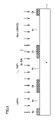
- FIG. 32 is a cross section of the semiconductor device according to the first embodiment.
- n + -buried diffusion layers (heavily doped impurity diffusion layers) 6 a , 6 b and 6 c are formed in a p ⁇ -type silicon substrate (semiconductor substrate) 1 , and n ⁇ -epitaxial growth layers (semiconductor layers) 7 a , 7 b and 7 c are formed at a main surface of silicon substrate 1 .
- a vertical npn bipolar transistor is formed in n ⁇ -epitaxial growth layer 7 a
- a lateral pnp bipolar transistor L-PNP
- an n-channel lateral DMOS transistor Nch-LDMOS
- a p-type diffusion layer (impurity diffusion layer) 17 a is formed at the surface of n ⁇ -epitaxial growth layer 7 a .
- This p-type diffusion layer 17 a forms a base (base-leading layer) of the vertical npn bipolar transistor.
- An n + -diffusion layer (heavily doped impurity diffusion layer) 21 a is formed at the surface of p-type diffusion layer 17 a .
- This n + -diffusion layer 21 a forms an emitter (emitter-leading layer) of the vertical npn bipolar transistor.
- p-type diffusion layers 17 b , 17 c and 17 d spaced from each other are formed at the surface of n ⁇ -epitaxial growth layer 7 b .
- p-type diffusion layers 17 b and 17 d form a collector of the lateral pnp transistor, and p-type diffusion layer 17 c forms an emitter of the lateral pnp bipolar transistor.
- n + -diffusion layer 21 c spaced from p-type diffusion layer 17 d is formed at the surface of epitaxial growth layer 7 b .
- n + -diffusion layer 21 c forms a base of the lateral pnp bipolar transistor.
- p-type diffusion layer (p-well) 62 At the surface of n ⁇ -epitaxial growth layer 7 c , p-type diffusion layer (p-well) 62 , n-type diffusion layer 67 and n + -diffusion layer 21 e neighboring. to each other are formed.
- p-type diffusion layer 17 e and n + -diffusion layer 21 d are formed.
- p-type diffusion layer 17 e functions as a back grate region of the lateral DMOS transistor, and n + -diffusion layer 21 d provides a source of the lateral DMOS transistor.
- n-type diffusion layer 67 forms an n ⁇ -drain of the lateral DMOS transistor.
- n-type diffusion layer 67 contains n-type impurities at a concentration from 1 ⁇ 10 16 cm ⁇ 3 to 1 ⁇ 10 18 cm ⁇ 3 , which is lower than those of n-type impurities in n + -diffusion layers 21 d and 21 e .
- n-type diffusion layer 67 is in contact with p-type diffusion layer 62 , and n + -diffusion layer 21 e is formed at the surface of n-type diffusion layer 67 .
- the concentration of n-type impurities contained in n-type diffusion layer 67 can be determined independently of various elements of the bipolar transistor. Therefore, by setting the n-type impurity concentration of the n-type diffusion layer 67 within the foregoing range, it is possible to lower the saturation voltage of the lateral DMOS transistor without lowering the breakdown voltage between the collector and base of the vertical npn bipolar transistor. Thus, the saturation resistance of the lateral DMOS transistor can be reduced.
- Field oxide films (insulating films) 54 a – 54 h are selectively formed on epitaxial growth layers 7 a – 7 c .
- Field oxide films 54 a , 54 c , 54 d , 54 f , 54 g and 54 h neighbor to the element isolating regions, i.e., p + -isolation diffusion layers 10 a – 10 d .
- Field oxide films 54 b and 54 e are formed between the bases and collectors of the vertical npn bipolar transistor and the lateral pnp bipolar transistor.
- field oxide films 54 a – 54 h By forming field oxide films 54 a – 54 h as described above, diffusion windows for forming the respective diffusion layers of the bipolar transistors can be determined by a mask for forming field oxide films 54 a – 54 h . Therefore, such a processing manner is not required that margins between the diffusion layers are ensured in every processing of forming the diffusion layer of the bipolar transistors. Accordingly, spaces between the diffusion layers can be small, and the density of the elements can be improved. A mask aligner apparatus having a high precision is not required in the process of forming the diffusion layers of the bipolar transistor so that a manufacturing cost can be reduced.
- Thermal oxide films (insulating films) 13 a , 13 b , 13 b 1 , 13 b 2 , 13 c , 13 c 1 , 13 d , 13 e , 13 e 1 , 13 e 2 , 13 f , 13 f 1 , 13 g , 13 h , 13 h 1 , 13 h 2 , 13 h 3 and 13 i are formed on epitaxial growth layers 7 a – 7 c located between field oxide films 54 a – 54 h.
- a gate electrode 57 is formed on a portion of oxide film 13 h 1 .
- An oxide film (insulating film) 63 partially covering gate electrode 57 is formed.
- First interlayer insulating films 22 a – 22 i are formed over field oxide films 54 a – 54 h , oxide films 13 a – 13 i , gate electrode 57 and oxide film 63 .
- First interlayer insulating films 22 a – 22 i may be formed of a CVD (Chemical Vapor Deposition) oxide film not doped with impurities.
- Second interlayer insulating films 23 a – 23 i are formed on first interlayer insulating films 22 a – 22 i , respectively.
- Second interlayer insulating films 23 a – 23 i may be formed of a CVD oxide film doped with impurities such as boron or phosphorus.
- First and second interlayer insulating films 22 a – 22 i and 23 a – 23 i are provided with a plurality of contact holes, which extend therethrough and reach n ⁇ -epitaxial growth layers 7 a – 7 c . More specifically, each of these contact holes reaches p-type diffusion layer 17 a , n + -diffusion layer 21 a , n + -diffusion layer 21 b , p-type diffusion layer 17 c , p-type diffusion layer 17 d , n + -diffusion layer 21 c , both of p-type diffusion layer 17 e and n + -diffusion layer 21 d , or n + -diffusion layer 21 e.
- First interconnections 25 a – 25 h are formed in the foregoing contact holes, respectively.
- First interconnections 25 a – 25 h may be made of a metal material such as Al, AlSi or AlCu.
- First interconnection 25 a serves as a base electrode of the vertical npn bipolar transistor.
- First interconnection 25 b serves as an emitter electrode of the vertical npn bipolar transistor.
- First interconnection 25 c serves as a collector electrode of the vertical npn bipolar transistor.
- First interconnection 25 d functions as an emitter electrode of the lateral pnp bipolar transistor.
- First interconnection 25 e functions as a collector electrode of the lateral pnp bipolar transistor.
- First interconnection 25 f functions as a base electrode of the lateral pnp bipolar transistor.
- First interconnection 25 g functions as a source electrode of the lateral DMOS transistor.
- First interconnection 25 h functions as a drain electrode of the lateral DMOS transistor.
- Third interlayer insulating films 26 a and 26 b are formed over second interlayer insulating films 23 a – 23 i and first interconnections 25 a – 25 h .
- Third interlayer insulating films 26 a and 26 b may be formed of a CVD oxide film.
- Third interlayer insulating films 26 a and 26 b are provided with through holes reaching first interconnections 25 , and a second interconnection 28 is formed in each through hole.
- Second interconnection 28 is covered with a protection film 29 , which may be made of a nitride film.
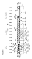
- FIG. 33 shows an example of a resistance portion of the semiconductor device according to the first embodiment.
- an n + -buried diffusion layer 6 d is formed in p ⁇ -type silicon substrate 1
- n ⁇ -epitaxial growth layer 7 d is formed at the main surface of silicon substrate 1 .
- p + -isolation diffusion layers 10 e and 10 f are formed on the opposite sides of n ⁇ -epitaxial growth layer 7 d , respectively
- p-type diffusion layer 17 i is formed at the surface of n ⁇ -epitaxial growth layer 7 d.
- the concentration of p-type impurities in p-type diffusion layer 17 i is in a range, e.g., from about 1 ⁇ 10 18 cm ⁇ 3 to about 1 ⁇ 10 19 cm ⁇ 3 .
- p-type diffusion layer 17 i is formed in a region surrounded by field oxide films 54 i and 54 j .
- p-type diffusion layer 17 i can be formed in the same steps as p-type diffusion layers 17 a – 17 e , in which case the concentration of p-type impurities in p-type diffusion layer 17 i is substantially in the same range as the concentration of p-type impurities in p-type diffusion layers 17 a – 17 e.
- Thermal oxide films 13 j – 13 l are formed on p + -isolation diffusion layers 10 e and 10 f , and thermal oxide films 13 k – 13 k 2 are formed on the surface of p-type diffusion layer 17 i .
- First interlayer insulating films 22 j – 22 l are formed over thermal oxide films 13 j – 13 l
- second interlayer insulating films 23 j – 23 l are formed over first interlayer insulating films 22 j – 22 l .
- a thermal oxidation process is performed to form a thermal oxide film (insulating film) 2 of about 1 ⁇ m in thickness on the main surface of p ⁇ -type silicon substrate 1 .
- Photoresist is applied to thermal oxide film 2 , and is patterned to have a predetermined configuration by photolithography. Thereby, photoresist patterns (masks) 3 a – 3 d having openings 4 a – 4 c are formed.
- thermal oxide film 2 masked with photoresist patterns 3 a – 3 d is etched.
- the etching can be performed by immersing it in an aqueous solution of hydrogen fluoride (HF).
- HF hydrogen fluoride
- n-type impurity ions 5 of antimony (Sb), arsenic (As) or the like are introduced into silicon substrate 1 masked with thermal oxide films 2 a – 2 d by an ion implanting method or the like.
- Thermal processing is performed to diffuse the introduced n-type impurities such as antimony so that n + -buried diffusion layers 6 a – 6 c are formed as shown in FIG. 4 .
- n + -buried diffusion layer 6 d is formed in the resistance portion shown in FIG. 33 .
- thermal oxide films 2 a – 2 d are removed.
- n ⁇ -epitaxial growth layer 7 of about 4 to about 6 ⁇ m in thickness.
- thermal oxide film 8 of about 0.05 ⁇ m in thickness is formed on n ⁇ -epitaxial growth layer 7 , and a low pressure CVD method is performed to deposit a nitride film (insulating film) 51 of about 0.1 ⁇ m in thickness on thermal oxide film 8 .
- photoresist patterns 52 a – 52 i having opening at predetermined positions are formed on nitride film 51 by a method similar to the foregoing method. Etching is effected on nitride film 51 masked with photoresist patterns 52 a – 52 i to form nitride films 51 a – 51 i having openings 53 a – 53 h.
- a thermal oxidation method using nitride films 51 a – 51 i as a mask is performed to form field oxide films 54 a – 54 h having a thickness, e.g., of about 0.6 ⁇ m.
- regions covered with nitride films 51 a – 51 i are not oxidized.
- 8 a – 8 i indicate thermal oxide films located around field oxide films 54 a – 54 h.
- nitride films 51 a – 51 i are removed with thermal phosphoric acid or the like.
- a low pressure CVD method or the like is performed to deposit, e.g., a nitride film 55 of about 0.1 ⁇ m in thickness covering field oxide films 54 a – 54 h and thermal oxide films 8 a – 8 i.
- nitride film 55 On nitride film 55 , a photoresist pattern (not shown) having openings at positions, where isolation diffusion layers are to be formed, is formed. Etching is effected on nitride film 55 and thermal oxide films 8 a , 8 d , 8 g and 8 i masked with the photoresist pattern. Thereby, as shown in FIG. 10 , openings 9 a – 9 d for forming the isolation diffusion layers are formed, and nitride films 55 a – 55 c are left. Thereafter, the photoresist pattern is removed.
- n ⁇ -epitaxial growth layer 7 is substantially divided into n ⁇ -epitaxial growth layers 7 a – 7 c.
- boron glass is first deposited.
- thermal processing is effected on a wafer for a predetermined time, e.g., from 10 to 30 minutes while flowing a B 2 H 6 gas at a low rate not exceeding 1 liter/minute, an O 2 gas at a low rate not exceeding 1 liter/minute and an N 2 gas at a high rate not exceeding 50 liter/minute into a diffusion furnace at a temperature of about 1000° C.
- the wafer is immersed in a dilute solution of HF to remove boron glass deposited on the wafer.
- thermal processing is performed to diffuse the boron.
- thermal oxide films 8 a , 8 d , 8 g and 8 i of about 0.1 ⁇ m in thickness are formed on p + -isolation diffusion layers 10 a – 10 d.
- p + -diffusion layers 10 e and 10 f are formed simultaneously with the formation of p + -isolation diffusion layers 10 a – 10 d . These layers define n ⁇ -epitaxial growth layer 7 d.
- a nitride film 56 e.g., of about 0.1 ⁇ m in thickness is formed as shown in FIG. 12 .
- a photoresist pattern (not shown) having openings on regions, in which n + -diffusion layer 12 is to be formed, is formed on nitride film 56 .
- Etching is effected on nitride film 56 and thermal oxide film 8 c masked with this photoresist pattern so that an opening 11 is formed as shown in FIG. 13 .
- nitride films 56 a and 56 b are left around opening 11 . Thereafter, the photoresist pattern is removed.
- n + -diffusion layer 12 reaching n + -buried diffusion layer 6 a is formed by a gas diffusion method using phosphorus.
- this gas diffusion method using phosphorus phosphorus glass is first deposited.
- thermal processing is effected on the wafer for a predetermined time, e.g., from 10 to 30 minutes while flowing a PH 3 gas at a low rate not exceeding 1 liter/minute, an O 2 gas at a low rate not exceeding 1 liter/minute and an N 2 gas at a high rate not exceeding 50 liter/minute into a diffusion furnace at a temperature of about 1000° C.
- thermal oxide film 8 c of about 0.1 ⁇ m in thickness is formed on n + -diffusion layer 12 .
- thermal oxide films 13 a – 13 i of about 0.01–0.02 ⁇ m in thickness are formed as shown in FIG. 15 .
- a portion of these thermal oxide films will form a gate oxide film of the lateral DMOS transistor.
- thermal oxide films 13 j – 13 l are formed in the resistance portion shown in FIG. 33 .
- a low pressure CVD method is performed to deposit a silicon film (semiconductor film) 57 , which has a thickness, e.g., of about 0.2 ⁇ m and is made of undoped polycrystalline silicon or amorphous silicon.
- a photoresist pattern 58 is formed on silicon film 57 .
- etching is effected on silicon film 57 masked with photoresist pattern 58 to form gate electrode 57 .
- processing is performed to form photoresist patterns 59 a and 59 b having an opening 60 located on a region, in which p-type diffusion layer 62 is to be formed.
- Boron ions are introduced into n ⁇ -epitaxial growth layer 7 c masked with photoresist patterns 59 a and 59 b by an ion implanting method.
- photoresist pattern 59 b may not completely cover gate electrode 57 due to misalignment of the mask. Therefore, photoresist patterns 59 a and 59 b are formed without removing photoresist pattern 58 on gate electrode 57 . By leaving photoresist pattern 58 on gate electrode 57 , such a situation can be prevented that boron ions 61 are implanted into n ⁇ -epitaxial growth layer 7 c through a portion of gate electrode 57 , which is not covered with photoresist pattern 59 b.
- thermal processing is performed to form p-type diffusion layer 62 .
- the surface of gate electrode 57 is oxidized to form oxide film 63 as shown in FIG. 18 .
- photoresist patterns 14 a – 14 f having an opening 15 a located on a region, in which p-type diffusion layer 17 a forming a base of the vertical npn bipolar transistor is to be formed, openings 15 b – 15 d located on regions, in which p-type diffusion layers 17 b – 17 d forming a collector and an emitter of the lateral pnp bipolar transistor are to be formed, and an opening 15 e located on a region, in which p-type diffusion layer 17 e forming a back gate of the lateral DMOS transistor is to be formed.
- an ion implanting method is performed to introduce boron ions 16 into n ⁇ -epitaxial growth layers 7 a – 7 c.
- p-type diffusion layers 17 a – 17 e are formed as shown in FIG. 20 .
- the base of the vertical npn bipolar transistor, the collector and emitter of the lateral pnp bipolar transistor and the back gate of the lateral DMOS transistor are simultaneously formed.
- p-type diffusion layer 17 i is formed simultaneously with formation of p-type diffusion layers 17 a – 17 e.
- processing is performed to form photoresist patterns 64 a and 64 b having an opening 65 on a region, in which the drain of the lateral DMOS transistor is to be formed.
- photoresist patterns 64 a and 64 b as a mask, phosphorus ions 66 are introduced into n ⁇ -epitaxial growth layer 7 c by an ion implanting method.
- thermal processing is performed. Thereby, n-type diffusion layer 67 is formed as shown in FIG. 22 .
- photoresist patterns 18 a – 18 f having openings respectively located on p-type diffusion layer 17 a and n + -diffusion layer 12 of the vertical npn bipolar transistor, on regions, in which the base of the lateral pnp bipolar transistor are to be formed, on regions, in which the source and drain of the lateral DMOS transistor are to be formed.
- photoresist patterns 18 a – 18 f as a mask, thermal oxide films 13 b , 13 c , 13 f , 13 h and 13 h 1 are etched to form openings 19 a – 19 e . This etching leaves thermal oxide films 13 b 1 , 13 c 1 , 13 f 1 and 13 h 2 at the positions neighboring to openings 19 a – 19 e.
- n-type impurity ions 20 of arsenic, phosphorus or the like are introduced into n ⁇ -epitaxial growth layers 7 a – 7 c by an ion implanting method.
- thermal processing is performed. This forms n + -diffusion layers 21 a – 21 e as shown in FIG. 24 .
- the emitter and the collector of the vertical npn bipolar transistor, the base of the lateral pnp bipolar transistor, and the source and drain of the lateral DMOS transistor are simultaneously formed.
- This thermal processing also forms oxide films on implantation openings 19 a – 19 e.
- FIGS. 25 and 26 are a perspective view and a plan of the semiconductor device in the state shown in FIG. 24 .
- p-type diffusion layers 17 b and 17 d are connected together to form the collector of the lateral pnp bipolar transistor.
- p-type diffusion layer 17 e forming the back gate of the lateral DMOS transistor is in contact with n + -diffusion layer 21 d , which will form the source of the lateral DMOS transistor.
- p-type diffusion layer 17 e and n + -diffusion layer 21 d have ends, of which corners are rounded, e.g., into an arc for ensuring an intended breakdown voltage.
- the source of the lateral DMOS transistor is formed of only a heavily doped impurity diffusion layer
- the drain of the lateral DMOS transistor is formed of a heavily doped impurity diffusion layer and a lightly doped impurity diffusion layer.
- a CVD method is then performed to deposit first interlayer insulating film 22 formed of a CVD oxide film, which has a thickness of about 0.2 ⁇ m and is, for example, not doped with impurities. Further, a CVD method is performed to deposit second interlayer insulating film 23 formed of a CVD oxide film, which has a thickness of about 0.6 ⁇ m and is doped with, e.g., boron or phosphorus. Then, appropriate thermal processing is performed to fluidize second interlayer insulating film 23 for flattening the wafer surface.
- a photoresist pattern (not shown) of a predetermined configuration is formed on second interlayer insulating film 23 .
- RIE Reactive Ion Etching
- This etching forms contact holes 24 a – 24 h as shown in FIG. 28 .
- First and second interlayer insulating films 22 a – 22 i and 23 a – 23 i are left around contact holes 24 a – 24 h . Also, thermal oxide films 13 b 1 , 13 b 2 , 13 c 1 , 13 e 1 , 13 e 2 , 13 f 1 , 13 h 1 , 13 h 2 and 13 h 3 are left.
- a contact hole for gate electrode 57 is formed at the same time.
- first and second interlayer insulating films 22 j and 23 are successively formed.
- a contact hole reaching p-type diffusion layer 17 i is also formed.
- first interconnections 25 a – 25 h are formed as shown in FIG. 29 .
- first interconnections 25 i and 25 j are formed in the resistance portion shown in FIG. 33 .
- a plasma CVD method or the like is performed to deposit a third interlayer insulating film, e.g., of about 0.8 ⁇ m made of a CVD oxide film.
- Photolithography and etching are performed to form a through hole 27 reaching first interconnection 25 c in the third interlayer insulating film, as shown in FIG. 30 . Consequently, third interlayer insulating films 26 a and 26 b remain around through hole 27 .
- a sputtering method or the like is performed to form a metal film (conductive film), which is made of AlSi, AlCu or the like and has a thickness, e.g., of about 1 ⁇ m, over the whole surface.
- a plasma CVD method or the like is performed to deposit a protection film (insulating film) 29 , e.g., of about 0.8 ⁇ m in thickness made of a CVD nitride film.
- FIGS. 34 to 37 A second embodiment of the invention will now be described with reference to FIGS. 34 to 37 .
- contact resistances may rise due to miniaturization of the elements. Accordingly, a device, which can suppress rising of the contact resistance, will now be described as a second embodiment.
- FIG. 37 shows an example of a distinctive structure of the semiconductor device according to the second embodiment.
- p + -diffusion layers (heavily doped impurity diffusion layers) 71 a , 71 b , 71 c and 71 d are formed at the surface of p-type diffusion layers 17 a , 17 c , 17 d and 17 e , respectively.
- p + -diffusion layers 71 a – 71 d contain p-type impurities at higher concentrations than p-type diffusion layers 17 a , 17 c , 17 d and 17 e , respectively.
- the concentrations of p-type impurities contained in p + -diffusion layers 71 a – 71 d are substantially in a range from about 1 ⁇ 10 19 cm ⁇ 3 to about 1 ⁇ 10 21 cm ⁇ 3 .
- Silicide layers 74 a – 74 h are formed at the surfaces of p + -diffusion layers 71 a – 71 d and n + -diffusion layers 21 a – 21 e .
- Silicide layers 74 a – 74 h may be titanium silicide (TiSi 2 ) layers. Titanium nitride (TiN) layers 73 a – 73 h extend continuously from silicide layers 74 a – 74 h over the sidewalls of the contact holes, respectively.
- First interconnections 25 a – 25 h are formed on titanium nitride layers 73 a – 73 h and silicide layers 74 a – 74 h , respectively. Structures other than the above are substantially the same as those of the first embodiment.
- silicide layers 74 a – 74 h are formed at the bottoms of the contact holes as described above, it is possible to reduce contact resistances between first interconnections 25 a – 25 h and the impurity diffusion layers.
- the heavily doped impurity diffusion layers such as p + -diffusion layers 71 a – 71 d at the surface of P-type impurity diffusion layers, it is possible to suppress rising of the contact resistance between the silicide layer and the silicon layer.
- the structure having contact holes 24 a – 24 h shown in FIG. 28 is formed through the steps similar to those in the first embodiment. Then, processing is performed to form photoresist patterns 68 a – 68 e having openings 69 a – 69 d , which continue to the contact holes on p-type diffusion layers 17 a , 17 c , 17 d and 17 e , respectively, on second interlayer insulating films 23 a – 23 i .
- p-type impurities 70 such as boron are introduced into p-type diffusion layers 17 a , 17 c , 17 d and 17 e .
- the p-type impurities are also introduced into the source of the lateral DMOS transistor. However, the source is already doped heavily with the n-type impurities. Therefore, no problem occurs in the characteristics of the lateral DMOS transistor.
- the p-type diffusion layers 17 a , 17 c , 17 d and 17 e are doped with p-type impurities.
- a titanium silicide layer is formed at the surfaces of p-type diffusion layers 17 a , 17 c , 17 d and 17 e formed by introducing boron (p-type impurities)
- boron p-type impurities
- p-type diffusion layer 17 a will form an intrinsic base of the vertical npn bipolar transistor, but the concentration of p-type impurities at the surface of p-type diffusion layer 17 a is in a range from about 1 ⁇ 10 18 to about 1 ⁇ 10 19 cm ⁇ 3 . Accordingly, the movement of impurities described above may disadvantageously increase the contact resistance.
- boron p-type impurities
- p-type impurities is added in advance into the surfaces of p-type diffusion layers 17 a , 17 c , 17 d and 17 e .
- n + -diffusion layers 21 a – 21 e are doped with n-type impurities at a concentration, which is ten or more times as large as those of p-type diffusion layers 17 a , 17 c , 17 d and 17 e . Therefore, even when the silicide layers are formed directly on the surfaces of n + -diffusion layers 21 a – 21 e , this increases the contact resistance only to an ignorable extent. Therefore, it is not necessary to add n-type impurities to n + -diffusion layers 21 a – 21 e.
- photoresist patterns 68 a – 68 e are removed, and thermal processing is performed at a relatively low temperature, e.g., of about 850° C. in an N 2 atmosphere.
- p + -diffusion layers 71 a – 71 d are formed at the surface of p-type diffusion layers 17 a , 17 c , 17 d and 17 e , respectively, as shown in FIG. 35 .
- a titanium film 72 of about 0.06 ⁇ m in thickness is deposited by a sputtering method or the like. Thermal processing is effected on titanium film 72 for tens of seconds at a relatively low temperature, e.g., of about 800° C. in the N 2 atmosphere.
- silicide layers (titanium silicide layers) 74 a – 74 h are formed at the surfaces of p + -diffusion layers 71 a – 71 d and n + -diffusion layers 21 a – 21 e , and titanium nitride layers 73 a – 73 h are formed on the sidewalls of the contact holes.
- a metal film e.g., of AlSi or AlCu having a thickness of 0.6 ⁇ m is then formed on the whole surface. Then, patterning is effected on this metal film and titanium nitride films 73 a – 73 h . Thereafter, the semiconductor device of the second embodiment is completed through the steps similar to those in the first embodiment.
- FIGS. 38–51 A third embodiment of the invention will now be described with reference to FIGS. 38–51 .
- a Hetero-junction Bipolar Transistor (HBT) of an SiGe base is a high-frequency bipolar transistor for use in the next generation of the ultra-high speed communication system (optical communication system of 10 Gb/s or higher, wireless LAN, mobile communication system and others).
- the base For producing a high-frequency npn transistor, it is necessary to reduce a thickness of the base. However, if the thickness of the base is reduced, it is difficult to ensure a collector-emitter breakdown voltage. Conversely, the collector-emitter breakdown voltage can be ensured by increasing the concentration of impurities in the base. However, this impedes ensuring of an intended base-emitter breakdown voltage.
- the base of the npn transistor may be made of an epitaxial growth layer (e.g., containing 10%–30% of Ge) of SiGe providing a narrower band gap than silicon.
- an epitaxial growth layer e.g., containing 10%–30% of Ge
- the base-emitter breakdown voltage can be ensured even if the base has a high impurity concentration. Accordingly, it is possible to use the base having a small thickness and a high impurity concentration.
- SiGe:C technique in which carbon (C) is added to SiGe (base).
- carbon (C) is added to SiGe (base) at a rate not exceeding, e.g., 1%, it is possible to suppress external diffusion of boron during thermal processing. In other words, the performance and reliability can be further improved.
- the foregoing problem relating to the base in the npn transistor is similar to the problem relating to the channel region in an nMOS transistor. More specifically, for reducing the gate length, it is necessary to increase the channel concentration for ensuring a punch through breakdown voltage between the drain and the source. However, this makes it difficult to ensure the breakdown voltage between the drain and the channel region.
- an epitaxial growth layer of SiGe or SiGe:C is utilized in the channel region of the lateral DMOS transistor, and thereby the lateral DMOS transistor having a further reduced gate length is produced.
- an epitaxial growth layer (compound semiconductor layer) 105 of SiGe or SiGe:C is formed at a surface of a p-type diffusion layer 104 .
- This epitaxial growth layer 105 forms a channel region of the lateral DMOS transistor.
- Epitaxial growth layer 105 has a thickness, e.g., from about 0.1 ⁇ m to about 0.3 ⁇ m, and contains p-type impurities at a concentration, e.g., from about 1 ⁇ 10 17 cm ⁇ 3 to 1 ⁇ 10 19 cm ⁇ 3 .
- the channel region can be heavily doped with impurities so that the channel length and the gate length can be reduced. Thereby, the lateral DMOS transistor having a further reduced gate length can be produced. Structures other than the above are substantially the same as those of the first embodiment.
- structures having thermal oxide film 8 c are formed through steps similar to those in the first embodiment, and thereafter, nitride films 56 a and 56 b shown in FIG. 14 are removed. Then, photoresist patterns 101 a and 101 b having opening 102 are formed on a region, in which p-type diffusion layer (p-well) 104 is to be formed. Using photoresist patterns 101 a and 101 b as a mask, p-type impurity ions 103 are implanted into n ⁇ -epitaxial growth layer 7 c by an ion implanting method as shown in FIG. 39 .
- Etching is effected on thermal oxide film 8 h masked with photoresist patterns 101 a and 101 b . Thereafter, photoresist patterns 101 a and 101 b are removed, and thermal processing is effected. This forms p-type diffusion layer 104 as shown in FIG. 40 .
- epitaxial growth layer 105 of SiGe or SiGe:C containing p-type impurities such as boron is formed on the exposed surface of p-type diffusion layer 104 by a selective epitaxial growth method.
- Epitaxial growth layer 105 has a thickness from about 0.1 ⁇ m to about 0.3 ⁇ m, and contains p-type impurities at a concentration from about 1 ⁇ 10 17 cm ⁇ 3 to 1 ⁇ 10 19 cm ⁇ 3 .
- thermal oxide films 8 a – 8 i are removed, and thermal oxide films 13 a – 13 i from about 0.01 to about 0.02 ⁇ m in thickness are formed. A portion of thermal oxide films 13 a – 13 i will form a gate oxide film of the lateral DMOS transistor.
- silicon film 57 which is about 0.2 ⁇ m in thickness and is made of polycrystalline silicon or amorphous silicon doped with phosphorus.
- Photoresist pattern 58 is formed on a portion of silicon film 57 , in which the gate electrode of the lateral DMOS transistor is to be formed.
- Etching is effected on silicon film 57 masked with photoresist pattern 58 . Thereby, gate electrode 57 is formed as shown in FIG. 42 . Gate electrode 57 is thermally oxidized to form oxide film 63 .
- photoresist patterns 14 a – 14 f having opening 15 a located on a region, in which p-type diffusion layer 17 a forming the base of the vertical npn bipolar transistor is to be formed, openings 15 b – 15 d located on regions, in which p-type diffusion layers 17 b – 17 d forming the collector and emitter of the lateral pnp bipolar transistor are to be formed, and opening 15 e located on a region, in which p-type diffusion layer 17 e forming the back gate of the lateral DMOS transistor is to be formed.
- photoresist patterns 14 a – 14 f as a mask, an ion implanting method is performed to introduce boron ions 16 into n ⁇ -epitaxial growth layers 7 a – 7 c.
- p-type diffusion layers 17 a – 17 e are formed as shown in FIG. 44 .
- the base of the vertical npn bipolar transistor, the collector and emitter of the lateral pnp bipolar transistor and the back gate of the lateral DMOS transistor are simultaneously formed.
- photoresist patterns 64 a and 64 b having opening 65 on a region, in which the drain of the lateral DMOS transistor is to be formed.
- photoresist patterns 64 a and 64 b as a mask, phosphorus ions 66 are introduced into n ⁇ -epitaxial growth layer 7 c by an ion implanting method.
- thermal processing is performed. Thereby, n-type diffusion layer (n ⁇ -drain) 67 is formed as shown in FIG. 46 .
- photoresist patterns 18 a – 18 f having openings located on p-type diffusion layer 17 a and n + -diffusion layer 12 of the vertical npn bipolar transistor, on a region, in which the base of the lateral pnp bipolar transistor is to be formed, and on regions, in which the source and drain of the lateral DMOS transistor are to be formed.
- photoresist patterns 18 a – 18 f as a mask, thermal oxide films 13 b , 13 c , 13 f , 13 h and 13 h 1 are etched to form openings 19 a – 19 e . This etching leaves thermal oxide films 13 b 1 , 13 c 1 , 13 f 1 and 13 h 2 at the positions neighboring to openings 19 a – 19 e.
- n-type impurity ions of arsenic, phosphorus or the like are introduced into n ⁇ -epitaxial growth layers 7 a – 7 c by an ion implanting method.
- thermal processing is performed. This forms n + -diffusion layers 21 a – 21 e as shown in FIG. 48 .
- the emitter and the collector of the vertical npn bipolar transistor, the base of the lateral pnp bipolar transistor, and the source and drain of the lateral DMOS transistor are simultaneously formed.
- This thermal processing also forms oxide films on implantation openings 19 a – 19 e.
- a CVD method is then performed to deposit first interlayer insulating film 22 formed of a CVD oxide film, which has a thickness of about 0.2 ⁇ m and is, for example, not doped with impurities. Further, a CVD method is performed to deposit second interlayer insulating film 23 formed of a CVD oxide film, which has a thickness of about 0.6 ⁇ m and is doped with, e.g., boron or phosphorus. Then, appropriate thermal processing is performed to fluidize second interlayer insulating film 23 for flattening the wafer surface.
- a photoresist pattern (not shown) of a predetermined configuration is formed on second interlayer insulating film 23 .
- dry etching with reactive ions is performed. This forms contact holes 24 a – 24 h as shown in FIG. 50 .
- First and second interlayer insulating films 22 a – 22 i and 23 a – 23 i remain around contact holes 24 a – 24 h , and also thermal oxide films 13 b 2 , 13 e 1 and 13 e 2 remain. Although not shown, a contact hole for gate electrode 57 is formed at the same time.
- a sputtering method or the like is performed to form a metal film, which is made of AlSi, AlCu or the like, and has a thickness, e.g., of about 0.6 ⁇ m, over the whole surface.
- a sputtering method or the like is performed to form a metal film, which is made of AlSi, AlCu or the like, and has a thickness, e.g., of about 0.6 ⁇ m, over the whole surface.
- first interconnections 25 a – 25 h are formed as shown in FIG. 51 .
- the semiconductor device of the third embodiment is completed through the steps similar to those in the first embodiment.
- An SOI (Silicon On Insulator) structure or a trench isolation structure may be employed for reducing a capacitance between the collector and p ⁇ -type silicon substrate 1 , and thereby improving high-frequency characteristics.
- the SOI structure and the trench isolation structure are employed in the semiconductor device equipped with bipolar transistors and lateral DMOS transistors prepared by using an epitaxial growth layer of SiGe or SiGe:C.
- FIG. 79 shows an example of a distinctive structure of the semiconductor device of the fourth embodiment.
- n ⁇ -silicon substrates (semiconductor layers) 111 a , 111 a 1 , 111 a 2 and 111 b as well as an epitaxial growth layer (p + -epitaxial growth layer: semiconductor layer) 105 are formed on p ⁇ -silicon substrate 1 with a thermal oxide film (insulating film) 112 therebetween.
- n ⁇ -silicon substrates 111 a , 111 a 1 , 111 a 2 and 111 b as well as epitaxial growth layer 105 correspond to the semiconductor layer in the SOI structure, and thermal oxide film 112 serves as the buried insulating film in the SOI structure.
- Epitaxial growth layer 105 is formed at the n ⁇ -silicon substrate, and reaches thermal oxide film 112 .
- Epitaxial growth layer 105 is made of SiGe or SiGe:C containing p-type impurities such as boron. By forming the epitaxial growth layer extending through the silicon substrate (semiconductor layer) to the buried insulating film as described above, the p-well can be formed in a self-aligning manner.
- Epitaxial growth layer 105 forms a channel region of the lateral DMOS transistor.
- Epitaxial growth layer 105 contains p-type impurities at a concentration from about 1 ⁇ 10 17 cm ⁇ 3 to 1 ⁇ 10 19 cm ⁇ 3 .
- a trench reaching thermal oxide film 112 is formed in the n ⁇ -silicon substrate, and is filled with oxide films 126 a – 126 d serving as isolating and insulating films. Further, n + -buried diffusion layers 119 a and 119 b reaching thermal oxide film 112 are formed at the bottoms of n ⁇ -silicon substrates 111 a and 111 a 1 . Structures other than the above are basically the same as those in the first embodiment.
- a thermal oxide film e.g., of about 0.1 ⁇ m in thickness is formed on n ⁇ -silicon substrate 111 , and a nitride film, e.g., of about 0.1 ⁇ m in thickness is formed on this thermal oxide film by a low pressure CVD method.
- oxide films 114 a and 114 b e.g., of about 1 ⁇ m in thickness are formed on this nitride film, and photoresist patterns 115 a and 115 b are formed on oxide films 114 a and 114 b.
- etching is performed to form an opening 116 .
- thermal oxide films 112 a and 112 b , nitride films 113 a and 113 b , and oxide films 114 a and 114 b are formed around opening 116 .
- Photoresist patterns 115 a and 115 b are removed, and etching is effected on n ⁇ -silicon substrate 111 masked with oxide films 114 a and 114 b by an RIE method. This etching forms a trench 117 as shown in FIG. 53 .
- Trench 117 provides a region for forming a well of the lateral DMOS transistor, and therefore must have a depth corresponding to a required performance of the lateral DMOS transistor. For example, it requires a depth from about 0.5 ⁇ m to about 2 ⁇ m.
- the region must have a sufficiently larger width as compared with the depth thereof so that the direction of the surface of the grown layer may coincide with that of n ⁇ -silicon substrate 111 .
- trench 117 must have a width one or more times as large as the depth.
- thermal oxidation is performed. This oxidation forms a thermal oxide film 172 of about 0.1 ⁇ m in thickness over the surface of trench 117 as shown in FIG. 54 . This thermal oxidation is so-called sacrificial oxidation, and is performed for removing etching damages at the surface of trench 117 . Using nitride films 113 a and 113 b as a mask, thermal oxide film 172 is removed from trench 117 .
- epitaxial growth layer (p + -epitaxial growth layer: semiconductor layer) 105 of SiGe or SiGe:C containing p-type impurities such as boron as shown in FIG. 55 .
- nitride films 113 a and 113 b as well as thermal oxide film 112 a and 112 b are removed.
- n ⁇ -silicon substrate 1 which is provided at its surface with thermal oxide film 112 of about 0.1 ⁇ m in thickness, is joined to n ⁇ -silicon substrate 111 .
- the surface of n ⁇ -silicon substrate 111 is polished by a CMP (Chemical Mechanical Polishing) method to expose epitaxial growth layer 105 .
- CMP Chemical Mechanical Polishing
- an oxide film 170 of about 1 ⁇ m in thickness is formed by a CVD method on epitaxial growth layer 105 and n ⁇ -silicon substrates 111 a and 111 b .
- Photoresist patterns 3 a – 3 c having openings at predetermined positions are formed on oxide film 170 .
- n-type impurity ions such as phosphorus or arsenic are implanted into n ⁇ -silicon substrate 111 a including its bottom with a high acceleration voltage from about 1 to about 2 MeV.
- n + -buried diffusion layers 119 a and 119 b are formed at the bottom of n ⁇ -silicon substrate 111 a as shown in FIG. 60 .
- processing is performed to form thermal oxide films 120 a – 120 c of about 0.1 ⁇ m in thickness, to form nitride films 121 a – 121 c of about 0.1 ⁇ m in thickness by a low pressure CVD method, and to form oxide films 122 a – 122 c of about 1 ⁇ m in thickness by a low pressure CVD method.
- Photoresist patterns 123 a – 123 c having openings are formed on oxide films 122 a – 122 c , respectively.
- Etching is effected on these oxide films and nitride films masked with photoresist patterns 123 a – 123 c . This etching forms openings 124 a – 124 d for trench isolation. Each of openings 124 a – 124 d has a width of about 0.5 ⁇ m.
- thermal oxide films 120 a – 120 c By forming openings 124 a – 124 d as described above, thermal oxide films 120 a – 120 c , nitride films 121 a – 121 c and oxide films 122 a – 122 c are left around openings 124 a – 124 d.
- Photoresist patterns 123 a – 123 c are removed, and etching is effected on n ⁇ -silicon substrates 111 a and 111 b masked with oxide films 122 a – 122 c by an RIE method. This forms trenches 125 a – 125 d reaching thermal oxide film 112 as shown in FIG. 62 . By forming trenches 125 a – 125 d , n ⁇ -silicon substrates 111 a 1 and 111 a 2 are left around trenches 125 a – 125 d.
- thermal oxidation is performed at a depth of about 0.1 ⁇ m. This forms oxide films 171 a – 171 f at the surfaces of trenches 125 a – 125 d.
- a CVD method is performed to form an oxide film 126 of about 1 ⁇ m in thickness covering n ⁇ -silicon substrates 111 a , 111 a 1 , 111 a 2 and 111 b .
- oxide film 126 a semiconductor film of polycrystalline silicon or amorphous silicon may be used.
- oxide film 126 is polished by a CPM method, and this polishing is stopped when nitride films 121 a – 121 c are exposed. Thereby, the trenches are filled with oxide films 126 a – 126 d as shown in FIG. 65 . Thereafter, nitride films 121 a – 121 c and thermal oxide films 120 a – 120 c are removed.
- Thermal oxidation is performed to form thermal oxide film 8 , e.g., of about 0.05 ⁇ m in thickness.
- Thermal oxide film 8 extends over n ⁇ -silicon substrates 111 a , 111 a 1 , 111 a 2 and 111 b , and also extends over oxide films 126 a – 126 d .
- a CVD method is performed to deposit a nitride film, e.g., of about 0.1 ⁇ m in thickness on thermal oxide film 8 .
- photoresist patterns 52 a – 52 i having openings at predetermined positions are formed.
- photoresist patterns 52 a – 52 i as a mask, etching is effected on the nitride film located on a region, in which field oxide films are to be formed. This etching forms openings 53 a – 53 h in the nitride film.
- nitride films 51 a – 51 i are left around openings 53 a – 53 h .
- photoresist patterns 52 a – 52 i are removed.
- thermal oxidation is performed. This forms field oxide films 54 a – 54 h , e.g., of about 0.2 ⁇ m in thickness as shown in FIG. 66 . Thereby, thermal oxide films 8 a – 8 i are left around field oxide films 54 a – 54 h.
- a CVD method is performed to deposit nitride film 56 of about 0.1 ⁇ m in thickness on thermal oxide films 8 a – 8 i as shown in FIG. 67 .
- a photoresist pattern (not shown) is formed on nitride film 56 , and etching is effected on nitride film 56 and thermal oxide film 8 c masked with this photoresist pattern. This forms a diffusion window used when forming a diffusion layer for leading out the collector of the vertical npn bipolar transistor. Nitride films 56 a and 56 b remain around the diffusion window thus formed as shown in FIG. 68 . Thereafter, the photoresist pattern is removed.
- a gas diffusion method using a phosphorus gas is performed to introduce phosphorus into n ⁇ -silicon substrate 111 a to form collector-leading n + -diffusion layer 12 , and phosphorus glass deposited on the wafer during the processing by the diffusion method is removed.
- thin thermal oxide film 8 c e.g., of about 0.1 ⁇ m in thickness is formed on the surface of n + -diffusion layer 12 .
- thermal oxide films 13 a – 13 i e.g., from about 0.01 to about 0.02 ⁇ m in thickness are formed as shown in FIG. 69 . Portions of thermal oxide films 13 a – 13 i form a gate oxide film of the lateral DMOS transistor.
- a low pressure CVD method is performed to deposit a silicon film (semiconductor film), which has a thickness, e.g., of about 0.2 ⁇ m and is made of polycrystalline silicon or amorphous silicon containing phosphorus.
- a photoresist pattern is formed on this silicon film and particularly at a position, where the gate electrode of the lateral DMOS transistor is to be formed.
- Etching is effected on the silicon film masked with the photoresist pattern thus formed. This forms gate electrode 57 as shown in FIG. 70 .
- Thermal oxidation is effected on the surface of gate electrode 57 to form oxide film 63 .
- photoresist patterns 14 a – 14 f having opening 15 a located on a region, in which p-type diffusion layer 17 a forming a base of the vertical npn bipolar transistor is to be formed, openings 15 b – 15 d located on regions, in which p-type diffusion layers 17 b – 17 d forming the collector and emitter of the lateral pnp bipolar transistor are to be formed, and opening 15 e located on a region, in which p-type diffusion layer 17 e forming the back gate of the lateral DMOS transistor is to be formed.
- photoresist patterns 14 a – 14 f as a mask, an ion implanting method is performed to introduce boron ions into n ⁇ -silicon substrates 111 a and 111 a 1 as well as epitaxial growth layer 105 .
- thermal processing is performed. This forms p-type diffusion layers 17 a – 17 e as shown in FIG. 72 .
- the base of the vertical npn bipolar transistor, the collector and emitter of the lateral pnp bipolar transistor and the back gate of the lateral DMOS transistor are formed at the same time.
- processing is performed to form photoresist patterns 64 a and 64 b having opening 65 on a region, in which the drain of the lateral DMOS transistor is to be formed.
- photoresist patterns 64 a and 64 b as a mask, phosphorus ions 66 introduced is introduced into n ⁇ -silicon substrate 111 b by an ion implanting method.
- thermal processing is performed. This forms n-type diffusion layer (n ⁇ -drain) 67 as shown in FIG. 74 .
- photoresist patterns 18 a – 18 f having openings on p-type diffusion layer 17 a and n + -diffusion layer 12 of the vertical npn bipolar transistor, on a region, in which the base of the lateral pnp bipolar transistor is to be formed, and regions, in which the source and drain of the lateral DMOS transistor are to be formed.
- photoresist patterns 18 a – 18 f as a mask, etching is effected on thermal oxide films 13 b , 13 c , 13 f , 13 h and 13 h 1 to form openings 19 a – 19 e . This etching leaves thermal oxide films 13 b 1 , 13 c 1 , 13 f 1 and 13 h 2 at positions neighboring to openings 19 a – 19 e.
- n-type impurity ions 20 such as arsenic or phosphorus ions are then introduced into n ⁇ -silicon substrates 111 a , 111 a 1 and 111 b as well as epitaxial growth layer 105 by an ion implanting method.
- thermal processing is performed. This forms n + -diffusion layers 21 a – 21 e as shown in FIG. 76 .
- the thermal processing simultaneously forms the emitter and the collector of the vertical npn bipolar transistor, the base of the lateral pnp bipolar transistor, and the source and drain of the lateral DMOS transistor. Also, the thermal processing forms oxide films on openings 19 a – 19 e for implantation.
- first interlayer insulating film 22 made of a CVD oxide film, which is, e.g., not doped with impurities and has a thickness of about 0.2 ⁇ m.
- second interlayer insulating film 23 made of a CVD oxide film, which is doped with, e.g., boron or phosphorus and has a thickness of about 0.6 ⁇ m.
- appropriate thermal processing is performed to fluidize second interlayer insulating film 23 for flattening the wafer surface.
- a photoresist pattern (not shown) of a predetermined configuration is formed on second interlayer insulating film 23 .
- dry etching is performed by an RIE method. This forms contact holes 24 a – 24 h as shown in FIG. 78 .
- First and second interlayer insulating films 22 a – 22 i and 23 a – 23 i remain around contact holes 24 a – 24 h , and also thermal oxide films 13 b 1 , 13 b 2 , 13 c 1 , 13 e 1 , 13 e 2 , 13 f 1 , 13 h 0 and 13 h 2 remain.
- a contact hole for gate electrode 57 is formed at the same time.
- a sputtering method or the like is performed to form a metal film, which is made of AlSi, AlCu or the like, and has a thickness, e.g., of about 0.6 ⁇ m, over the whole surface.
- a sputtering method or the like is performed to form a metal film, which is made of AlSi, AlCu or the like, and has a thickness, e.g., of about 0.6 ⁇ m, over the whole surface.
- first interconnections 25 a – 25 h are formed as shown in FIG. 79 .
- the semiconductor device of the fourth embodiment is completed through the steps similar to those in the first embodiment.
- the lateral npn bipolar transistor is employed, and a selective epitaxial growth technique of SiGe or SiGe:C is applied to the lateral npn bipolar transistor and the lateral pnp bipolar transistor.
- An epitaxial growth layer of SiGe or SiGe:C is used in the base of the lateral npn bipolar transistor, whereby a capacitance between the collector and the base can be significantly reduced, and the lateral npn bipolar transistor capable of operation with a higher frequency than the vertical type can be achieved.
- the epitaxial growth layer of SiGe or SiGe:C is used in the emitter and the collector of the lateral npn bipolar transistor, whereby a layer doped with p-type impurities more heavily than a silicon layer can be employed, and a higher current drive performance can be achieved.
- FIG. 105 shows an example of a distinctive structure of the semiconductor device of the fifth embodiment.
- n ⁇ -silicon substrates (semiconductor layers) 111 a , 111 b , 111 b 1 , 111 c , 111 d , 111 e , 111 e 1 and 111 f as well as epitaxial growth layers 105 a – 105 e correspond to the semiconductor layer in the SOI structure, and thermal oxide film 112 serves as the buried insulating film in the SOI structure.
- Epitaxial growth layers 105 a – 105 e are formed at the n ⁇ -silicon substrate, and reach thermal oxide film 112 .
- Epitaxial growth layers 105 a – 105 e are made of SiGe or SiGe:C containing p-type impurities such as boron.
- the base of the lateral npn bipolar transistor is formed at the surface of epitaxial growth layer 105 a
- the collector of the lateral pnp bipolar transistor is formed at the surfaces of epitaxial growth layers 105 b and 105 d
- the emitter of lateral pnp bipolar transistor is formed at the surface of the epitaxial growth layer 105 c .
- epitaxial growth layer 105 e forms the channel region of the lateral DMOS transistor.
- the concentration of p-type impurities contained in epitaxial growth layers 105 a – 105 e is substantially in a range, e.g., from about 1 ⁇ 10 17 cm ⁇ 3 to about 1 ⁇ 10 19 cm ⁇ 3 .
- Trenches reaching thermal oxide film 112 are formed in the n ⁇ -silicon substrate, and are filled with oxide films 126 a – 126 d serving as the isolating and insulating films. Further, n + -diffusion layers 12 a – 12 c reaching thermal oxide film 112 are formed in n ⁇ -silicon substrates 111 a and 111 b . n + -diffusion layers 21 a – 21 c are formed at the surfaces of n + -diffusion layers 12 a – 12 c , respectively.
- n + -diffusion layers 21 a and 21 c form the collectors of the lateral npn bipolar transistor
- n + -diffusion layer 21 b forms the emitter of the lateral npn bipolar transistor.
- n + -diffusion layer 21 d is formed at the surface of n ⁇ -silicon substrate 111 e
- n + -diffusion layer 21 e is formed at the surface of epitaxial growth layer 105 e
- an n + -diffusion layer 21 f is formed at the surface of n ⁇ -silicon substrate 111 f .
- n + -diffusion layers 21 e and 21 f form the source and drain of the lateral DMOS transistor, respectively. Structures other than the above are basically the same as those of the fourth embodiment.
- a thermal oxide film e.g., of about 0.1 ⁇ m in thickness is formed on n ⁇ -silicon substrate 111 , and a nitride film, e.g., of about 0.1 ⁇ m in thickness is formed on this thermal oxide film by a low pressure CVD method.
- a low pressure CVD method an oxide film, e.g., of about 1 ⁇ m in thickness is formed on this nitride film, and photoresist patterns 115 a – 115 f are formed on this oxide film.
- etching is performed to form openings 116 a – 116 e .
- thermal oxide films 112 a – 112 f , nitride films 113 a – 113 f and oxide films 114 a – 114 f are formed around openings 116 a – 116 e.
- Photoresist patterns 115 a – 115 f are removed, and etching is effected on n ⁇ -silicon substrate 111 masked with oxide films 114 a – 114 f by an RIE method. This forms trenches 117 a – 117 e as shown in FIG. 81 .
- Trenches 117 a – 117 e are regions for forming the well of the lateral DMOS transistor as well as the base, emitter and collector of the bipolar transistors, and therefore must have a depth corresponding to required performances of these transistors. For example, a depth from 0.5 ⁇ m to 2 ⁇ m is required.
- thermal oxidation is performed. As shown in FIG. 82 , this thermal oxidation forms thermal oxide films 172 a – 172 e of about 0.1 ⁇ m in thickness at the surfaces of trenches 117 a to 117 e , respectively. Thereby, etching damages at the surfaces of trenches 117 a – 117 e can be removed. Thereafter, etching is performed to remove thermal oxide films 172 a – 172 e on trenches 117 a – 117 e using nitride films 113 a – 113 f as a mask.
- a selective epitaxial growth method is performed to form epitaxial growth layers (p + -epitaxial growth layers) 105 a – 105 e of SiGe or SiGe:C containing p-type impurities such as boron.
- the concentration of p-type impurities contained in epitaxial growth layers 105 a – 105 e is substantially in a range from about 1 ⁇ 10 17 cm ⁇ 3 to about 1 ⁇ 10 19 cm ⁇ 3 .
- Epitaxial growth layer 105 a provides a region for forming the base of the lateral npn bipolar transistor, and epitaxial growth layers 105 b and 105 d provide a region for forming the collector of the lateral pnp bipolar transistor. Also, epitaxial growth layer 105 c provides a region for forming the emitter of the lateral pnp bipolar transistor, and epitaxial growth layer 105 e provides a region for forming the p-well of the lateral DMOS transistor.
- nitride films 113 a – 113 f and thermal oxide films 112 a – 112 f are removed. Thereafter, as shown in FIG. 84 , p ⁇ -silicon substrate 1 provided at its surface with thermal oxide film 112 of about 0.1 ⁇ m in thickness is bonded to n ⁇ -silicon substrate 111 .
- processing is them performed to form thermal oxide films 120 a – 120 c of about 0.1 ⁇ m in thickness, to form nitride films 121 a – 121 c of about 0.1 ⁇ m in thickness by a low pressure CVD method, and to form oxide films 122 a – 122 c of about 1 ⁇ m in thickness by a low pressure CVD method.
- Photoresist patterns 123 a – 123 c having openings on oxide films 122 a – 122 c are formed.
- photoresist patterns 123 a – 123 c as a mask, etching is effected on the oxide films and the nitride films. Thereby, openings 124 a – 124 d for trench isolation are formed. Each of openings 124 a – 124 d has a width of about 0.5 ⁇ m.
- thermal oxide films 120 a – 120 c By forming openings 124 a – 124 d as described above, thermal oxide films 120 a – 120 c , nitride films 121 a – 121 c and oxide films 122 a – 122 c are left around openings 124 a – 124 d.
- Photoresist patterns 123 a – 123 c are removed, and etching is effected on n ⁇ -silicon substrates 111 a , 111 b , 111 e and 111 f masked with oxide films 122 a – 122 c by an RIE method. This forms trenches 125 a – 125 d reaching thermal oxide film 112 as shown in FIG. 87 .
- n ⁇ -silicon substrates 111 b 1 and 111 e 1 are left around trenches 125 a – 125 d.
- thermal oxidation is performed at a depth of about 0.1 ⁇ m. This forms oxide films 171 a – 171 f at the surfaces of trenches 125 a – 125 d as shown in FIG. 88 .
- oxide film 126 of about 1 ⁇ m in thickness covering n ⁇ -silicon substrates 111 a – 111 f .
- a semiconductor film e.g., of polycrystalline silicon or amorphous silicon may be used.
- oxide film 126 is polished by a CPM method, and this polishing is stopped when nitride films 121 a – 121 c are exposed. Thereby, the trenches are filled with oxide films 126 a – 126 d as shown in FIG. 90 . Thereafter, nitride films 121 a – 121 c and thermal oxide films 120 a – 120 c are removed.
- thermal oxide film 8 of about 0.5 ⁇ m in thickness.
- Thermal oxide film 8 is formed not only on n ⁇ -silicon substrates 111 a – 111 f but also on oxide films 126 a – 126 d .
- a nitride film of about 0.1 ⁇ m in thickness is formed by a CVD method.
- photoresist patterns 52 a – 52 j having openings at predetermined positions are formed.
- photoresist patterns 52 a – 52 j as a mask, etching is effected on the nitride film located on the region, in which the field oxide film is to be formed. This forms openings 53 a – 53 i in the nitride film.
- nitride films 51 a – 51 j are left around openings 53 a – 53 i .
- photoresist patterns 52 a – 52 j are removed.
- thermal oxidation is performed. This forms field oxide films 54 a – 54 i of about 0.2 ⁇ m in thickness as shown in FIG. 91 . Thereby, thermal oxide films 8 a – 8 j are left around field oxide films 54 a – 54 i.
- nitride film 56 After removing nitride films 51 a – 51 j , e.g., with hot phosphoric acid, a CVD method is performed to form nitride film 56 of about 0.1 ⁇ m in thickness on thermal oxide films 8 a – 8 j as shown in FIG. 92 .
- a photoresist pattern (not shown) is formed on nitride film 56 , and etching is effected on nitride film 56 and thermal oxide films 8 b – 8 d masked with the photoresist pattern thus formed.
- This forms diffusion windows 127 a – 127 c for forming diffusion layers used for leading out the emitter and the collector of the lateral npn bipolar transistor. Around these diffusion windows, nitride films 56 a – 56 d remain as shown in FIG. 93 . Thereafter, the photoresist patterns are removed.
- a gas diffusion method using phosphorus is performed to introduce the phosphorus through diffusion windows 127 a – 127 c into n ⁇ -silicon substrates 111 a and 111 b as well as epitaxial growth layer 105 a .
- n + -diffusion layer 12 b for leading out the emitter and n + -diffusion layers 12 a – 12 c for leading out the collector are formed as shown in FIG. 94 .
- processing is performed to remove phosphorus glass, which was deposited on the wafer during execution of the gas diffusion method.
- a thermal oxide film of about 0.1 ⁇ m in thickness is formed at the surface of n + -diffusion layers 12 a – 12 c.
- thermal oxide films 13 a – 13 j e.g., from about 0.01 to about 0.02 ⁇ m in thickness are formed as shown in FIG. 94 . Portions of thermal oxide films 13 a – 13 j will form the gate oxide film of the lateral DMOS transistor.
- a low pressure CVD method is performed to deposit a silicon film (semiconductor film), which is, e.g., 0.2 ⁇ m in thickness and is made of polycrystalline silicon or amorphous silicon doped with phosphorus.
- a photoresist pattern is formed on a portion of this silicon film, in which the gate electrode of the lateral DMOS transistor is to be formed. Etching is effected on the silicon film masked with this photoresist pattern. This forms gate electrode 57 as shown in FIG. 95 .
- the surface of gate electrode 57 is thermally oxidized to form oxide film 63 .
- photoresist patterns 14 a – 14 g having openings 15 a and 15 b located on a region, in which the base-leading layer ( 17 a and 17 b ) of the lateral npn bipolar transistor is to be formed, openings 15 c – 15 e located on a region, in which p-type diffusion layers 17 c – 17 e forming the collector and emitter of the lateral pnp bipolar transistor are to be formed, and opening 15 f located on a region, in which p-type diffusion layer 17 f forming the back gate of the lateral DMOS transistor is to be formed.
- photoresist patterns 14 a – 14 g as a mask, an ion implanting method is performed to introduce boron ions into n ⁇ -silicon substrates 111 a and 111 b as well as epitaxial growth layers 105 a , 105 c , 105 d and 105 e.
- thermal processing is performed. This forms p-type diffusion layers 17 a – 17 f as shown in FIG. 97 .
- the base of the lateral npn bipolar transistor, the collector and emitter of the lateral pnp bipolar transistor and the back gate of the lateral DMOS transistor are simultaneously formed.
- processing is performed to form photoresist patterns 64 a and 64 b having opening 65 located on a region, in which the drain of the lateral DMOS transistor is to be formed.
- photoresist patterns 64 a and 64 b as a mask, an ion implanting method is performed to introduce phosphorus ions into n ⁇ -silicon substrate 111 f .
- thermal processing is performed. This forms n-type diffusion layer (n ⁇ -drain) 67 as shown in FIG. 99 .
- processing is performed to form photoresist patterns 18 a – 18 g having openings located on n + -diffusion layers 12 a – 12 c of the lateral npn bipolar transistor, on a region, in which the base of the lateral pnp bipolar transistor is to be formed, and on regions, in which the source and drain of the lateral DMOS transistor are to be formed.
- photoresist patterns 18 a – 18 g as a mask, etching is effected on thermal oxide films 13 b , 13 c , 13 d , 13 g , 13 i and 13 i 1 to form openings 19 a – 19 f.
- photoresist patterns 18 a – 18 g as a mask, an ion implanting method is performed to introduce n-type impurity ions such as arsenic ions or phosphorus ions into n ⁇ -silicon substrates 111 a , 111 b , 111 e and 111 f as well as epitaxial growth layers 105 a and 105 e .
- thermal processing is performed. This forms n + -diffusion layers 21 a – 21 f as shown in FIG. 101 .
- the emitter and collector of the lateral npn bipolar transistor, the base of the lateral pnp bipolar transistor, and the source and drain of the lateral DMOS transistor are simultaneously formed.
- This thermal processing also forms oxide films on implantation openings 19 a – 19 f.
- FIG. 102 is a plan of the semiconductor device in the state shown in FIG. 101 .
- n + -diffusion layers 12 a and 12 c are the collector of the lateral npn bipolar transistor
- p-type diffusion layers 17 a and 17 b are the base of the lateral npn bipolar transistor.
- Epitaxial growth layers 105 b and 105 d are isolated, and both form the collector of the lateral pnp bipolar transistor. A leading electrode must be provided for each of epitaxial growth layers 105 b and 105 d .
- the collector may have a form shown in FIG. 142 .
- first interlayer insulating film 22 made of a CVD oxide film, which is, e.g., not doped with impurities and has a thickness of about 0.2 ⁇ m.
- second interlayer insulating film 23 made of a CVD oxide film, which is doped with, e.g., boron or phosphorus and has a thickness of about 0.6 ⁇ m.
- appropriate thermal processing is performed to fluidize second interlayer insulating film 23 for flattening the wafer surface.
- a photoresist pattern (not shown) of a predetermined configuration is formed on second interlayer insulating film 23 .
- dry etching is performed by an RIE method. This etching forms contact holes 24 a – 24 i as shown in FIG. 104 .
- First and second interlayer insulating films 22 a – 22 j and 23 a – 23 j remain around contact holes 24 a – 24 i , and also thermal oxide films 13 c 2 , 13 f 1 , 13 f 2 and 13 f 3 remain.
- a contact hole for gate electrode 57 is formed at the same time.
- a sputtering method or the like is performed to form a metal film, which is, e.g., about 0.6 ⁇ m in thickness and is made of AlSi, AlCu or the like, over the whole surface.
- a metal film which is, e.g., about 0.6 ⁇ m in thickness and is made of AlSi, AlCu or the like, over the whole surface.
- first interconnections 25 a – 25 i are formed as shown in FIG. 105 .
- the semiconductor device of the fifth embodiment is completed through the steps similar to those in the first embodiment.
- DPSA Double Polysilicon Self-Align
- an emitter electrode and a base electrode are partially formed of polycrystalline silicon or amorphous silicon, and a position of an emitter opening is determined in a self-aligning manner.
- the emitter electrode and the base electrode of the lateral npn bipolar transistor are partially made of silicon films (semiconductor films) of polycrystalline silicon or amorphous silicon.
- silicon films semiconductor films
- polycrystalline silicon or amorphous silicon is advantageous because it exhibits a small particle diameter and allows easy working, as compared with metal materials.
- FIG. 125 shows an example of a distinctive structure of a semiconductor device according to a sixth embodiment.
- an emitter electrode of the lateral npn bipolar transistor is formed of first interconnection 25 b and an emitter-leading pad layer 163
- a base electrode is formed of first interconnection 25 a and a base-leading pad layer ( 152 a and 152 b ).
- An n + -diffusion layer (heavily doped impurity diffusion layer) 162 is formed under emitter-leading pad layer 163 .
- Emitter-leading pad layer 163 extends over the base-leading pad layer ( 152 a and 152 b ) with oxide films 156 a , 156 b and 160 therebetween, and these oxide films electrically insulate and isolate emitter-leading pad layer 163 from the base-leading pad layer.
- the gate electrode of the lateral DMOS transistor is formed of a multilayer structure of the silicon films. By patterning these silicon films, the silicon film forming an upper layer of the gate electrode and the base-leading pad layer are formed. Structures other than the above are basically the same as those in the fifth embodiment.
- structures including thermal oxide films 13 a – 13 j are formed through steps similar to those in the fifth embodiment. Thereafter, a low pressure CVD method is performed to deposit a silicon film (semiconductor film) 151 , which has a thickness, e.g., of about 0.1 ⁇ m and is made of polycrystalline silicon or amorphous silicon doped with phosphorus.
- a photoresist pattern (not shown) of a predetermined configuration is formed on silicon film 151 . Using the photoresist pattern as a mask, silicon film 151 is etched.
- silicon films 151 a – 151 i are left on the trench isolating region, the collector of the lateral npn bipolar transistor, the lateral pnp bipolar transistor and the lateral DMOS transistor as shown in FIG. 107 .
- a silicon film (semiconductor layer) 152 e.g., of about 0.1 ⁇ m in thickness, which is made of polycrystalline silicon or amorphous silicon not doped with impurities.
- p-type impurities 55 such as BF 2 ions are introduced into silicon film 152 by an ion implanting method. In this processing, an acceleration voltage is controlled to prevent the implanted ions from penetrating silicon film 152 .
- the p-type impurity ions may be introduced into silicon film 152 without using a mask. In this case, steps for mask alignment or the like can be eliminated so that the steps can be simplified.
- silicon film 152 will form a part of the gate electrode of the lateral DMOS transistor.
- phosphorus (n-type impurities) introduced into silicon film 151 h forming a lower layer is diffused into silicon film 152 for operating it as an n-type gate electrode, it is therefore necessary to determine the concentrations of p-type impurities and phosphorus (n-type impurities) so that the concentration of p-type impurities may be much lower than that of phosphorus (n-type impurities).
- oxide film 156 e.g., of about 0.1 ⁇ m in thickness.
- oxide film 156 and silicon film 152 are left as shown in FIG. 112 .
- a thermal oxide film 159 e.g., of about 0.01 ⁇ m in thickness is formed at the surface of epitaxial growth layer 105 a as shown in FIG. 112 .
- a low pressure CVD method is performed to deposit an oxide film 160 , e.g., of about 0.1 ⁇ m in thickness.
- etching is effected on oxide film 160 and thermal oxide film 159 by an RIE method to form an opening exposing the surface of epitaxial growth layer 105 a .
- a sidewall insulating film made of oxide film 160 is formed on sidewalls of oxide films 156 a and 156 b defining the opening.
- oxide films 156 a and 156 b as a mask, arsenic ions are introduced into the surface of epitaxial growth layer 105 a . Thereafter, thermal processing is performed to form n + -diffusion layer 162 forming the emitter of the lateral npn bipolar transistor at the surface of epitaxial growth layer 105 a (i.e., the surface of n + -diffusion layer 12 b )as shown in FIG. 115 .
- a low pressure CVD method is performed to deposit a silicon film (semiconductor film) 163 , e.g., of about 0.1 ⁇ m in thickness made of polycrystalline silicon or amorphous silicon.
- arsenic ions are implanted into silicon film 163 .
- a photoresist pattern of a predetermined configuration is formed on silicon film 163 , and etching is effected on silicon film 163 and oxide films 156 a and 156 b masked with this photoresist pattern by an RIE method.
- silicon film 163 and oxide films 156 a and 156 b are patterned to form a pad layer 163 for leading out the emitter.
- Oxide films 156 a and 156 b remain under emitter-leading pad layer 163 .
- a photoresist pattern of a predetermined configuration is formed on silicon films 152 a and 152 b , and etching is effected on silicon films 152 a and 152 b masked with this photoresist pattern by an RIE method.
- silicon films 152 a and 152 b are patterned to form pad layer ( 152 a and 152 b ) for leading out the base as shown in FIG. 117 .
- a multilayer structure of silicon films 151 h and 152 b 1 is left on epitaxial growth layer 105 e . This multilayer structure forms the gate electrode of the lateral DMOS transistor. Thereafter, photoresist pattern is removed.
- photoresist patterns 14 a – 14 g having openings 15 a and 15 b located on a region, in which the base-leading layer ( 17 a and 17 b ) of the lateral npn bipolar transistor is to be formed, openings 15 c – 15 e located on a region, in which p-type diffusion layers 17 c – 17 e forming the collector and emitter of the lateral pnp bipolar transistor are to be formed, and opening 15 f located on a region, in which p-type diffusion layer 17 f forming the back gate of the lateral DMOS transistor is to be formed.
- photoresist patterns 14 a – 14 g as a mask, boron ions are introduced by an ion implanting method into n ⁇ -silicon substrates 111 a and 111 b as well as epitaxial growth layers 105 b , 105 c , 105 d and 105 e.
- thermal processing is performed. This forms p-type diffusion layers 17 a – 17 f as shown in FIG. 119 .
- the thermal processing simultaneously forms the base of the lateral npn bipolar transistor, the collector and emitter of the lateral pnp bipolar transistor, and the back gate of the lateral DMOS transistor.
- This thermal processing also forms thermal oxide film 63 a covering emitter-leading pad layer 163 and the base-leading pad layer ( 152 a and 152 b ), and forms thermal oxide film 63 b covering the gate electrode ( 151 h and 152 b 1 ) of the lateral DMOS transistor.
- photoresist patterns 64 a and 64 b having opening 65 are formed on a region, in which the drain of the lateral DMOS transistor is to be formed.
- photoresist patterns 64 a and 64 b as a mask, phosphorus ions 66 are introduced into n ⁇ -silicon substrate 111 f by an ion implanting method.
- thermal processing is performed. This forms n-type diffusion layer (n ⁇ -drain) 67 as shown in FIG. 121 .
- processing is performed to form photoresist patterns 18 a – 18 g having openings located on n + -diffusion layers 12 a – 12 c of the lateral npn bipolar transistor, on a region, in which the base of the lateral npn bipolar transistor is to be formed, and on regions, in which the source and drain of the lateral DMOS transistor are to be formed.
- Etching is effected on thermal oxide films 13 b , 63 a , 13 d , 13 g , 13 i and 13 i 1 masked with photoresist patterns 18 a – 18 g to form openings 19 a – 19 f.
- n-type impurity ions 20 such as arsenic or phosphorus ions are then introduced by an ion implanting method into n ⁇ -silicon substrates 111 a , 111 b , 111 e and 111 f , epitaxial growth layer 105 e and emitter-leading pad layer 163 .
- thermal processing is performed. This forms n + -diffusion layers 21 a and 21 c – 21 f as shown in FIG. 123 .
- the thermal processing simultaneously forms the collector of the lateral npn bipolar transistor, the base of the lateral pnp bipolar transistor, and the source and drain of the lateral DMOS transistor.
- This thermal processing also forms a thermal oxide film on implantation openings 19 a – 19 f.
- first interlayer insulating film 22 made of a CVD oxide film, which is, e.g., not doped with impurities and has a thickness of about 0.2 ⁇ m.
- second interlayer insulating film 23 made of a CVD oxide film, which is doped with, e.g., boron and phosphorus, and has a thickness of about 0.6 ⁇ m.
- appropriate thermal processing is performed to fluidize second interlayer insulating film 23 for flattening the wafer surface.
- a photoresist pattern (not shown) of a predetermined configuration is formed on second interlayer insulating film 23 .
- dry etching is performed by an RIE method. This forms contact holes 24 a – 24 i as shown in FIG. 124 .
- First and second interlayer insulating films 22 a – 22 j and 23 a – 23 j remain around contact holes 24 a – 24 i , and also thermal oxide films 63 a , 63 a 1 , 63 a 2 , 13 d 1 , 13 f 1 , 13 f 2 , 13 f 3 , 13 g 1 , 13 i 0 and 13 i 2 remain.
- a contact hole for the gate electrode ( 152 b 1 and 151 h ) is formed at the same time.
- a sputtering method or the like is performed to form a metal film, which is, e.g., about 0.6 ⁇ m in thickness and is made of AlSi, AlCu or the like, over the whole surface.
- a metal film which is, e.g., about 0.6 ⁇ m in thickness and is made of AlSi, AlCu or the like, over the whole surface.
- first interconnections 25 a – 25 i are formed as shown in FIG. 125 .
- the semiconductor device of the sixth embodiment is completed through the steps similar to those in the first embodiment.
- a seventh embodiment will now be described with reference to FIGS. 126 to 146 .
- the lateral npn bipolar transistor is likewise employed, and a selective epitaxial growth technique of SiGe or SiGe:C is applied to the lateral npn bipolar transistor and the lateral pnp bipolar transistor.
- the epitaxial growth layer of SiGe or SiGe:C has a reduced thickness, and the impurity diffusion layers and the electrodes forming the bipolar transistors have devised planar configurations.
- epitaxial growth layers 105 a – 105 e of SiGe or SiGe:C and n ⁇ -silicon substrates 111 a – 111 f have reduced thicknesses in a range from about 0.2 ⁇ m to about 0.4 ⁇ m. This facilitates working and processing (opening, filling and others) of the trenches. Also, provision of n + -diffusion layers 12 a – 12 c is eliminated. This can reduce steps. Further, n + -diffusion layers 21 a – 21 f and p-type diffusion layers 17 a – 17 f reach thermal oxide film 112 , which is the buried insulating film. Thereby, the lateral transistor can be formed.
- n + -diffusion layers 21 a and 21 c form the collector of the lateral npn bipolar transistor
- p-type diffusion layers 17 a , 17 b , 17 g and 17 h form the base of the lateral npn bipolar transistor.
- p-type diffusion layers 17 a , 17 b , 17 g and 17 h are arranged on the four corners of epitaxial growth layer 105 a .
- the plurality of p-type diffusion layers 17 a , 17 b , 17 g and 17 h spaced from each other are arranged along the outer periphery of epitaxial growth layer 105 a so that true base 105 a can be opposed to collectors 21 a and 21 c . Since external base ( 17 a , 17 b , 17 g and 17 h ) are electrode-leading layers of true base 105 a , these portions do not substantially affect the transistor operation.
- n + -diffusion layers 21 a and 21 c partially protrude inward (i.e., toward p + -diffusion layer 105 a ).
- collectors 21 and 21 c , true base 105 a and external base 17 a , 17 b , 17 g and 17 h ) are spaced by different distances.
- Epitaxial growth layers 105 b and 105 d are isolated from each other. Each of epitaxial growth layers 105 b and 105 d is the collector of the lateral pnp bipolar transistor, and requires the leading electrode. The collector may have a configuration shown in FIG. 102 .
- FIGS. 143A and 143B show a modification of a layout of the lateral npn bipolar transistor.
- n + -diffusion layer 21 b forming the emitter of the lateral npn bipolar transistor has a circular planar form
- each of epitaxial growth layer 105 a , n ⁇ -silicon substrate 111 a and n + -diffusion layers 21 a and 21 c has an annular planar form.
- p-type diffusion layers 17 a , 17 b , 17 g and 17 h are arranged with spaces therebetween, and n + -diffusion layers 21 a and 21 c located between p-type diffusion layers 17 a , 17 b , 17 g and 17 h protrude inward.
- the respective regions have substantially concentric outer peripheries so that it is possible to suppress variations in characteristics due to misalignment of masks. Structures other than the above are substantially the same as those of the fifth embodiment.
- a thermal oxide film e.g., of about 0.1 ⁇ m in thickness is formed on n ⁇ -silicon substrate 111 , and a nitride film, e.g., of about 0.1 ⁇ m in thickness is formed on the thermal oxide film thus formed by a low pressure CVD method.
- a nitride film e.g., of about 0.1 ⁇ m in thickness is formed on this nitride film, and photoresist patterns 115 a – 115 f are formed on this oxide film.
- etching is performed to form openings 116 a – 116 e .
- thermal oxide films 112 a – 112 f , nitride films 113 a – 113 f and oxide films 114 a – 114 f are left around openings 116 a – 116 e.
- etching is effected on n ⁇ -silicon substrate 111 masked with oxide films 114 a – 114 f by an RIE method. This forms trenches 117 a – 117 e as shown in FIG. 127 .
- Trenches 117 a – 117 e have a depth, which is required for the epitaxial growth layer to be formed in a later step, and is, e.g., in a range from about 0.5 ⁇ m to about 2 ⁇ m.
- thermal oxidation is performed. This oxidation forms thermal oxide films 172 a – 172 e of about 0.1 ⁇ m in thickness at the surfaces of trenches 117 a – 117 e as shown in FIG. 128 . Thereby, etching damages at the surfaces of trenches 117 a – 117 e can be removed. Using nitride films 113 a – 113 f as a mask, etching is then performed to remove thermal oxide films 172 a – 172 e on trenches 117 a – 117 e.
- epitaxial growth layers p + -epitaxial growth layers
- a selective epitaxial growth method is performed to form epitaxial growth layers (p + -epitaxial growth layers) 105 a – 105 e of SiGe or SiGe:C containing p-type impurities such as boron as shown in FIG. 129 .
- the concentration of p-type impurities contained in epitaxial growth layers 105 a – 105 e is substantially in a range from about 1 ⁇ 0 17 cm ⁇ 3 to about 1 ⁇ 10 19 cm ⁇ 3 .
- Epitaxial growth layer 105 a provides a region for forming the base of the lateral npn bipolar transistor
- epitaxial growth layers 105 b and 105 d provide a region for forming the collector of the lateral pnp bipolar transistor
- epitaxial growth layer 105 c provides a region for forming the emitter of the lateral pnp bipolar transistor
- epitaxial growth layer 105 e provides a region for forming the p-well of the lateral DMOS transistor.
- nitride films 113 a – 113 f and thermal oxide films 112 a – 112 f are removed. Thereafter, as shown in FIG. 130 , p ⁇ -silicon substrate 1 provided at its surface with thermal oxide film 112 of about 0.1 ⁇ m in thickness is bonded to n ⁇ -silicon substrate 111 .
- n ⁇ -silicon substrate 111 is polished by a CMP method, and this polishing stops when epitaxial growth layers 105 a – 105 e achieve an intended thickness.
- epitaxial growth layers 105 a – 105 e have a reduced thickness, e.g., from about 0.2 ⁇ m to about 4 ⁇ m. Consequently, n ⁇ -silicon substrates (semiconductor layers) 111 a – 111 f are left around epitaxial growth layers 105 a – 105 e.
- processing is them performed to form thermal oxide films of about 0.1 ⁇ m in thickness, to form nitride films of about 0.1 ⁇ m in thickness by a low pressure CVD method, and to form oxide films of about 1 ⁇ m in thickness by a low pressure CVD method.
- Photoresist patterns 123 a – 123 c having openings on these oxide films are formed. Using photoresist patterns 123 a – 123 c as a mask, etching is effected on the oxide films and the nitride films. Thereby, openings 124 a – 124 d for trench isolation are formed. Each of openings 124 a – 124 d has a width of about 0.5 ⁇ m.
- thermal oxide films 120 a – 120 c By forming openings 124 a – 124 d as described above, thermal oxide films 120 a – 120 c , nitride films 121 a – 121 c and oxide films 122 a – 122 c are left around openings 124 a – 124 d.
- Photoresist patterns 123 a – 123 c are removed, and etching is effected on n ⁇ -silicon substrates 111 a , 111 b , 111 e and 111 f masked with oxide films 122 a – 122 c by an RIE method. This forms trenches 125 a – 125 d reaching thermal oxide film 112 as shown in FIG. 133 .
- n ⁇ -silicon substrates 111 b 1 and 111 e 1 are left around trenches 125 a – 125 d.
- thermal oxidation is performed at a depth of about 0.1 ⁇ m. This forms oxide films 171 a – 171 f at the surfaces of trenches 125 a – 125 d as shown in FIG. 134 .
- oxide film 126 of about 1 ⁇ m in thickness covering n ⁇ -silicon substrates 111 a – 111 f .
- a semiconductor film e.g., of polycrystalline silicon or amorphous silicon may be used.
- oxide film 126 is polished by a CPM method, and this polishing is stopped when nitride films 121 a – 121 c are exposed. Thereby, the trenches are filled with oxide films 126 a – 126 d as shown in FIG. 136 . Thereafter, nitride films 121 a – 121 c and thermal oxide films 120 a – 120 c are removed.
- thermal oxide film 13 is formed not only on n ⁇ -silicon substrates 111 a – 111 f but also on oxide films 126 a – 126 d . Thermal oxide film 13 will partially form the gate oxide film of the lateral DMOS transistor.
- a low pressure CVD method is performed to deposit a silicon film (semiconductor film), which is about 0.2 ⁇ m in thickness and is made of polycrystalline silicon or amorphous silicon doped with phosphorus.
- a photoresist pattern (not shown) is formed on a portion of this silicon film, in which the gate electrode of the lateral DMOS transistor is to be formed. Etching is effected on the silicon film masked with this photoresist pattern. This forms gate electrode 57 as shown in FIG. 136 .
- the surface of gate electrode 57 is thermally oxidized to form oxide film 63 .
- photoresist patterns 14 a – 14 g having openings 15 a and 15 b located on a region, in which the base-leading layer ( 17 a and 17 b ) of the lateral npn bipolar transistor is to be formed, openings 15 c – 15 e located on a region, in which p-type diffusion layers 17 c – 17 e forming the collector and emitter of the lateral pnp bipolar transistor are to be formed, and an opening 15 f located on a region, in which p-type diffusion layer 17 f forming the back gate of the lateral DMOS transistor is to be formed.
- photoresist patterns 14 a – 14 g as a mask, an ion implanting method is performed to introduce boron ions into n ⁇ -silicon substrates 111 a and 111 b as well as epitaxial growth layers 105 a , 105 c , 105 d and 105 e.
- thermal processing is performed. This forms p-type diffusion layers 17 a – 17 h as shown in FIG. 137 .
- the base of the lateral npn bipolar transistor, the collector and emitter of the lateral pnp bipolar transistor and the back gate of the lateral DMOS transistor are simultaneously formed.
- processing is performed to form photoresist patterns 64 a and 64 b having opening 65 located on a region, in which the drain of the lateral DMOS transistor is to be formed.
- photoresist patterns 64 a and 64 b as a mask, an ion implanting method is performed to introduce phosphorus ions into n ⁇ -silicon substrate 111 f .
- thermal processing is performed. This forms n-type diffusion layer (n ⁇ drain) 67 as shown in FIG. 139 .
- processing is performed to form photoresist patterns 18 a – 18 g having openings located on regions, in which n + -diffusion layers 12 a – 12 c of the lateral npn bipolar transistor are to be formed, on a region, in which the base of the lateral pnp bipolar transistor is to be formed, and on regions, in which the source and drain of the lateral DMOS transistor are to be formed.
- thermal oxide film 13 is etched using photoresist patterns 18 a – 18 g as a mask, etching is effected on thermal oxide film 13 to form openings 19 a – 19 f This leaves thermal oxide films 13 a , 13 b , 13 b 1 , 13 c , 13 d , 13 e and 13 f around openings 19 a – 19 f.
- photoresist patterns 18 a – 18 g as a mask, an ion implanting method is performed to introduce n-type impurity ions such as arsenic ions or phosphorus ions into n ⁇ -silicon substrates 111 a , 111 b , 111 e and 111 f as well as epitaxial growth layers 105 a and 105 e .
- thermal processing is performed. This forms n + -diffusion layers 21 a – 21 f as shown in FIG. 141 .
- FIG. 142 is a plan of the semiconductor device shown in FIG. 141 .
- first interlayer insulating film 22 made of a CVD oxide film, which is, e.g., not doped with impurities and has a thickness of about 0.2 ⁇ m.
- second interlayer insulating film 23 made of a CVD oxide film, which is doped with, e.g., boron and phosphorus, and has a thickness of about 0.6 ⁇ m.
- appropriate thermal processing is performed to fluidize second interlayer insulating film 23 for flattening the wafer surface.
- a photoresist pattern (not shown) of a predetermined configuration is formed on second interlayer insulating film 23 .
- dry etching is performed by an RIE method. This forms contact holes 24 a – 24 i as shown in FIG. 145 .
- First and second interlayer insulating films 22 a – 22 j and 23 a – 23 j remain around contact holes 24 a – 24 i , and also thermal oxide films 13 a , 13 b , 13 c , 13 d , 13 d 1 , 13 d 2 , 13 d 3 , 13 e , 13 f , 13 f 1 and 13 g remain.
- a contact hole for gate electrode 57 is formed at the same time.
- a sputtering method or the like is performed to form a metal film, which is, e.g., about 0.6 ⁇ m in thickness and is made of AlSi, AlCu or the like, over the whole surface.
- a metal film which is, e.g., about 0.6 ⁇ m in thickness and is made of AlSi, AlCu or the like, over the whole surface.
- first interconnections 25 a – 25 i are formed as shown in FIG. 146 .
- the semiconductor device of the seventh embodiment is completed through the steps similar to those in the first embodiment.
- the DPSA technique is applied to the lateral npn bipolar transistor of the seventh embodiment already described. More specifically, the emitter electrode and the base electrode of the lateral npn bipolar transistor are partially formed of a silicon film (semiconductor film) of polycrystalline silicon, amorphous silicon or the like.
- the emitter electrode of the lateral npn bipolar transistor is formed of first interconnection 25 b and emitter-leading pad layer 163
- the base electrode is formed of first interconnection 25 a and the base-leading pad layer ( 152 a and 152 b ).
- n + -diffusion layer 162 is formed under emitter-leading pad layer 163 .
- Emitter-leading pad layer 163 extends over the base-leading pad layer ( 152 a and 152 ) with oxide films 156 a , 156 b and 160 therebetween, and these oxide films electrically isolate emitter-leading pad layer 163 from the base-leading pad layer. Structures other than the above are basically the same as those of the seventh embodiment.
- the trenches are filled with oxide films 126 a – 126 d . Thereafter, nitride films 121 a – 121 c and thermal oxide films 120 a – 120 c are removed.
- Thermal oxidation is further performed to form thermal oxide film 8 , e.g., of about 0.5 ⁇ m in thickness as shown in FIG. 147 .
- Thermal oxide film 8 is formed not only on n ⁇ -silicon substrate 111 a – 111 f but also on oxide films 126 a – 126 d .
- a CVD method or the like is performed to deposit a nitride film, e.g., of about 0.1 ⁇ m in thickness on thermal oxide film 8 , and photoresist patterns 52 a – 52 d of a predetermined configuration are formed on the nitride film.
- photoresist patterns 52 a – 52 d as a mask, etching is effected on the nitride film to form openings 53 a – 53 c located on a region, in which the field oxide film is to be formed. Nitride films 51 a – 51 d remain around openings 53 a – 53 c . Thereafter, photoresist patterns 52 a – 52 d are removed.
- nitride films 51 a – 51 d as a mask, thermal oxidation is performed to form field oxide films 54 a – 54 c , e.g., of about 0.2 ⁇ m in thickness as shown in FIG. 148 . Thereafter, nitride films 51 a – 51 d and thermal oxide films 8 a – 8 d are removed.
- thermal oxidation is performed to form thermal oxide films 13 a – 13 d , e.g., from about 0.01 to about 0.02 ⁇ m in thickness as shown in FIG. 149 .
- a portion of thermal oxide film 13 d forms the gate oxide film of the lateral DMOS transistor.
- a low pressure CVD method is performed to deposit silicon film (semiconductor film) 151 , e.g., of about 0.2 ⁇ m in thickness, which is made of polycrystalline silicon or amorphous silicon doped with phosphorus.
- silicon film 151 On silicon film 151 , a photoresist pattern (not shown) of a predetermined configuration is formed. Using this photoresist pattern as a mask, silicon film 151 is etched. Thereby, as shown in FIG. 150 , silicon films 151 a – 151 a are left on the trench isolating region, the collector of the lateral npn bipolar transistor, the lateral pnp bipolar transistor and the lateral DMOS transistor.
- silicon film (semiconductor film) 152 which is made of polycrystalline silicon or amorphous silicon not doped with impurities, and has a thickness, e.g., of about 0.1 ⁇ m in thickness.
- photoresist patterns 153 a and 153 b as a mask p-type impurity ions such as BF 2 ions are introduced into silicon film 152 by an ion implanting method. In this processing, an acceleration voltage is controlled to prevent the implanted ions from penetrating silicon film 152 .
- the p-type impurity ions may be introduced into silicon film 152 without using a mask. In this case, steps for mask alignment or the like can be eliminated, and the steps can be simplified.
- silicon film 152 will form a part of the gate electrode of the lateral DMOS transistor.
- phosphorus (n-type impurities) introduced into silicon film 151 c forming a lower layer is diffused into silicon film 152 for operating it as an n-type gate electrode, it is therefore necessary to determine the concentrations of p-type impurities and phosphorus (n-type impurities) so that the concentration of p-type impurities may be much lower than that of phosphorus (n-type impurities).
- oxide film 156 e.g., of about 0.1 ⁇ m in thickness.
- oxide film 156 and silicon film 152 are etched using photoresist patterns 157 a and 157 b as a mask. etching is effected on oxide film 156 and silicon film 152 . This forms an opening exposing the surface of epitaxial growth layer 105 a . Around this opening, oxide films 156 a and 156 b as well as silicon films 152 a and 152 b are left as shown in FIG. 154 .
- thermal oxide film 159 e.g., of about 0.01 ⁇ m in thickness is formed as shown in FIG. 154 .
- a low pressure CVD method is performed to deposit oxide film 160 , e.g., of about 0.1 ⁇ m in thickness.
- Etching is effected on oxide film 160 and thermal oxide film 159 by an RIE method to form an opening exposing the surface of epitaxial growth layer 105 a .
- a sidewall insulating film made of oxide film 160 is formed on sidewalls of oxide films 156 a and 156 b defining the opening.
- oxide films 156 a and 156 b as a mask, arsenic ions are introduced into the surface of epitaxial growth layer 105 a . Thereafter, thermal processing is performed to form n + -diffusion layer 162 forming the emitter of the lateral npn bipolar transistor at the surface of epitaxial growth layer 105 a as shown in FIG. 156 .
- a low pressure CVD method is performed to deposit silicon film (semiconductor film) 163 , e.g., of about 0.1 ⁇ m in thickness made of polycrystalline silicon or amorphous silicon. Then, arsenic ions are implanted into silicon film 163 .
- a photoresist pattern of a predetermined configuration is formed on silicon film 163 , and etching is effected on silicon film 163 and oxide films 156 a and 156 b masked with this photoresist pattern by an RIE method.
- silicon film 163 and oxide films 156 a and 156 b are patterned to form emitter-leading pad layer 163 as shown in FIG. 157 .
- Oxide films 156 a and 156 b remain under emitter-leading pad layer 163 .
- a photoresist pattern of a predetermined configuration is formed on silicon films 152 a and 152 b , and etching is effected on silicon films 152 a and 152 b masked with this photoresist pattern by an RIE method.
- silicon films 152 a and 152 b are patterned to form the base-leading pad layer ( 152 a and 152 b ) as shown in FIG. 158 .
- a multilayer structure of silicon films 151 c and 152 b 1 is left on epitaxial growth layer 105 e . This multilayer structure forms the gate electrode of the lateral DMOS transistor. Thereafter, photoresist pattern is removed.
- processing is then performed to form photoresist patterns 14 a – 14 g having openings 15 a and 15 b located on a region, in which the base-leading layer ( 17 a and 17 b ) of the lateral npn bipolar transistor is to be formed, openings 15 c – 15 e located on a region, in which p-type diffusion layers 17 c – 17 e forming the collector and emitter of the lateral pnp bipolar transistor are to be formed, and opening 15 f located on a region, in which p-type diffusion layer 17 f forming the back gate of the lateral DMOS transistor is to be formed.
- photoresist patterns 14 a – 14 g as a mask, p-type impurities such as boron ions are introduced by an ion implanting method into n ⁇ -silicon substrates 111 a and 111 b as well as epitaxial growth layers 105 b , 105 c , 105 d and 105 e.
- thermal processing is performed. This forms p-type diffusion layers 17 a – 17 f as shown in FIG. 160 .
- the thermal processing simultaneously forms the base of the lateral npn bipolar transistor, the collector and emitter of the lateral pnp bipolar transistor, and the back gate of the lateral DMOS transistor.
- This thermal processing also forms thermal oxide film 63 a covering emitter-leading pad layer 163 and the base-leading pad layer ( 152 a and 152 b ), and forms thermal oxide film 63 b covering the gate electrode ( 151 h and 152 b 1 ) of the lateral DMOS transistor.
- photoresist patterns 64 a and 64 b having opening 65 are formed on a region, in which the drain of the lateral DMOS transistor is to be formed.
- photoresist patterns 64 a and 64 b as a mask, n-type impurities such as phosphorus ions are introduced into n ⁇ -silicon substrate 111 f by an ion implanting method.
- thermal processing is performed. This forms n-type diffusion layer (n ⁇ -drain) 67 as shown in FIG. 162 .
- processing is performed to form photoresist patterns 18 a – 18 g having openings located on a region, in which the emitter and collector of the lateral npn bipolar transistor is to be formed, on a region, in which the base of the lateral pnp bipolar transistor is to be formed, and on regions, in which the source and drain of the lateral DMOS transistor are to be formed.
- Etching is effected on thermal oxide films 13 b , 63 a , 13 d , 63 a , 13 d and 13 d 1 masked with photoresist patterns 18 a – 18 g to form openings 19 a – 19 f.
- n-type impurity ions 20 such as arsenic or phosphorus ions are then introduced by an ion implanting method into n ⁇ -silicon substrates 111 a , 111 b ; 111 e and 111 f , epitaxial growth layer 105 e and emitter-leading pad layer 163 .
- thermal processing is performed. This forms n + -diffusion layers 21 a and 21 c – 21 f as shown in FIG. 164 .
- the thermal processing simultaneously forms the collector of the lateral npn bipolar transistor, the base of the lateral pnp bipolar transistor, and the source and drain of the lateral DMOS transistor.
- This thermal processing also forms a thermal oxide film on implantation openings 19 a – 19 f.
- first interlayer insulating film 22 made of a CVD oxide film, which is, e.g., not doped with impurities and has a thickness of about 0.2 ⁇ m.
- second interlayer insulating film 23 made of a CVD oxide film, which is doped with, e.g., boron and phosphorus, and has a thickness of about 0.6 ⁇ m.
- appropriate thermal processing is performed to fluidize second interlayer insulating film 23 for flattening the wafer surface.
- a photoresist pattern (not shown) of a predetermined configuration is formed on second interlayer insulating film 23 .
- dry etching is performed by an RIE method. This etching forms contact holes 24 a – 24 i as shown in FIG. 165 .
- First and second interlayer insulating films 22 a – 22 j and 23 a – 23 j remain around contact holes 24 a – 24 i , and also thermal oxide films 63 a , 63 a 1 , 63 a 2 , 13 c , 13 c 1 , 13 c 2 , 13 c 3 , 13 c 4 , 13 d , 13 d 1 , 13 d 2 , 63 b , 13 d 3 and 13 d 4 remain.
- a contact hole for gate electrode ( 152 b 1 and 151 c ) is formed at the same time.
- a sputtering method or the like is performed to form a metal film, which is, e.g., about 0.6 ⁇ m in thickness and is made of AlSi, AlCu or the like, over the whole surface.
- a metal film which is, e.g., about 0.6 ⁇ m in thickness and is made of AlSi, AlCu or the like, over the whole surface.
- first interconnections 25 a – 25 i are formed as shown in FIG. 166 .
- the semiconductor device of the eighth embodiment is completed through the steps similar to those in the first embodiment.
- a semiconductor device includes a semiconductor substrate of a first conductivity type; a semiconductor layer of a second conductivity type formed on the semiconductor substrate; a field insulating film formed selectively on a surface of the semiconductor layer; an element isolating region of the first conductivity type extending from the surface of the semiconductor layer to the semiconductor substrate, and isolating each of elements; a gate electrode of a DMOS transistor formed on the semiconductor layer with a gate insulating film therebetween; a well region of the first conductivity type formed at the surface of the semiconductor layer, and extending from a source side of the DMOS transistor to a position under the gate electrode; a first impurity diffusion layer of the first conductivity type formed at the surface of the semiconductor layer, and functioning as a base of a first bipolar transistor; a second impurity diffusion layer of the first conductivity type formed at the surface of the semiconductor layer, and functioning as a resistance; third and fourth impurity diffusion layers of the first conductivity
- the first bipolar transistor is an npn bipolar transistor
- the second bipolar transistor is a pnp bipolar transistor
- the emitter of the second bipolar transistor is connected to a power supply terminal
- a base of the second bipolar transistor is connected to an input terminal
- the collector of the second bipolar transistor is connected to the base of the first bipolar transistor
- a collector of the first bipolar transistor is connected to the power supply terminal via a resistance
- an emitter of the first bipolar transistor is connected to an output terminal and a drain of the DMOS transistor
- a gate of the DMOS transistor is connected to an inverted input terminal
- a source and the back gate region of the DMOS transistor are grounded.
- the semiconductor device described above includes an interlayer insulating film covering the first bipolar transistor, the second bipolar transistor and the DMOS transistor, and having contact holes reaching the first to tenth impurity diffusion layers and the gate electrode of the DMOS transistor; a heavily doped impurity diffusion layer of the first conductivity type formed at surfaces of the first, second, third, fourth and fifth impurity diffusion layers located immediately under the contact holes; a silicide layer formed at a surface of the heavily doped impurity diffusion layer; a nitride metal layer extending from an end of the silicide layer to a position on a sidewall of the contact hole; and an interconnection formed on the silicide layer and the nitride metal layer.
- a channel region of the DMOS transistor is formed of a compound semiconductor layer of the first conductivity type containing silicon and germanium (Ge) or containing silicon, germanium and carbon.
- a semiconductor device includes a semiconductor substrate of a first conductivity type; a semiconductor layer of a second conductivity type formed on the semiconductor substrate with an insulating film therebetween; a field insulating film formed selectively on a surface of the semiconductor layer; an element isolating region extending from a surface of the semiconductor layer to the semiconductor substrate, and isolating each of elements; a compound semiconductor layer of the first conductivity type extending through the semiconductor layer to the insulating film, and containing a combination of silicon and germanium (Ge) or a combination of silicon, germanium and carbon; a gate electrode of a DMOS transistor formed on the compound semiconductor layer with a gate insulating film therebetween; a first impurity diffusion layer of the first conductivity type formed at the surface of the semiconductor layer, and functioning as a base of a first bipolar transistor; a second impurity diffusion layer of the first conductivity type formed at the surface of the semiconductor layer, and functioning as a resistance; third and fourth impurity diffusion layers of
- a semiconductor device includes a semiconductor substrate of a first conductivity type; a semiconductor layer of a second conductivity type formed on the semiconductor substrate with an insulating film therebetween; a field insulating film formed selectively on a surface of the semiconductor layer; an element isolating region extending from a surface of the semiconductor layer to the semiconductor substrate, and isolating each of elements; a first compound semiconductor layer of the first conductivity type extending through the semiconductor layer to the insulating film, containing a combination of silicon and germanium (Ge) or a combination of silicon, germanium and carbon, and having a region to be used as a base of a first bipolar transistor; second and third compound semiconductor layers extending through the semiconductor layer to the insulating film, containing a combination of silicon and germanium (Ge) or a combination of silicon, germanium and carbon, and having regions to be used as an emitter and a collector of a second bipolar transistor; a fourth compound semiconductor layer extending through the semiconductor layer to the insulating film
- the first impurity diffusion layer preferably has a plurality of first protruding regions protruding outward
- the eighth impurity diffusion layer preferably has a second protruding region protruding inward toward a position between the first protruding regions.
- the first, seventh and eighth impurity diffusion layers preferably have concentric forms.
- a gate electrode of the DMOS transistor is preferably formed of a layered structure of a first semiconductor layer forming a lower layer portion and a second semiconductor layer forming an upper layer portion, and the semiconductor device preferably includes a base-leading electrode of the first bipolar transistor located on the first impurity diffusion layer and formed of the second semiconductor layer, and an emitter-leading electrode of the first bipolar transistor located on the seventh impurity diffusion layer, and formed of a third semiconductor layer isolated from the base-leading electrode by an insulating film.
- impurities of the second conductivity type are diffused from the first semiconductor layer into the second semiconductor layer of the gate electrode such that the second semiconductor layer of the gate electrode attains the second conductivity type, and the base-leading electrode of the first bipolar transistor made of the second semiconductor layer attains the first conductivity type.
- the invention also provides a method of manufacturing a semiconductor device including a first bipolar transistor having a base of a first conductivity type, a second bipolar transistor having a base of a second conductivity type, and a DMOS transistor, and the method includes the following steps.
- a semiconductor layer of a second conductivity type is formed on a semiconductor substrate of the first conductivity type.
- a field insulating film is selectively formed on a surface of the semiconductor layer. Impurities of the first conductivity type are selectively introduced into the surface of the semiconductor layer to form an element isolating region extending from the surface of the semiconductor layer to the semiconductor substrate, and isolating each of elements.
- a gate electrode of the DMOS transistor is formed on the semiconductor layer with a gate insulating film therebetween.
- Impurities of the first conductivity type are selectively introduced into the surface of the semiconductor layer to form a well region extending from the source side of the DMOS transistor to a position under the gate electrode. Impurities of the first conductivity type are selectively introduced into the surface of the semiconductor layer to form a first impurity diffusion layer functioning as a base of a first bipolar transistor, a second impurity diffusion layer functioning as a resistance, third and fourth impurity diffusion layers functioning as an emitter and a collector of the second bipolar transistor, and a fifth impurity diffusion layer functioning as a back gate region of the DMOS transistor and located at the surface of the well region.
- Impurities of the second conductivity type are selectively introduced into the semiconductor layer to form a lightly doped region of a drain of the DMOS transistor. Impurities of the second conductivity type are selectively introduced into the semiconductor layer to form a sixth impurity diffusion layer functioning as the drain of the DMOS transistor, seventh and eighth impurity diffusion layers functioning as emitter- and collector-leading layers of the first bipolar transistor, a ninth impurity diffusion layer functioning as a base-leading layer of the second bipolar transistor, and a tenth impurity diffusion layer functioning as a source of the DMOS transistor.
- the method of manufacturing the semiconductor device further includes the following steps.
- An interlayer insulating film covering the first and second bipolar transistors and the DMOS transistor is formed.
- Contact holes reaching the first to tenth impurity diffusion layers and the gate electrode of the DRAM transistor are formed in the interlayer insulating film.
- a mask is formed to expose contact holes reaching the first to fifth impurity diffusion layers, and to cover the contact holes reaching the sixth to tenth impurity diffusion layers and the gate electrode of the DMOS transistor.
- impurities of the first conductivity type are introduced into the surfaces of the first and third to fifth impurity diffusion layers to form a heavily doped impurity diffusion layer. The mask is removed.
- a metal film extending into the contact holes is formed on the interlayer insulating film.
- Thermal processing is effected on the metal film in a nitrogen atmosphere to form a silicide layer at the surface of the heavily doped impurity diffusion layer, and to change the metal film on a sidewall of the contact hole into a metal nitride film.
- An interconnection is formed on the silicide layer and the metal nitride film.
- the method includes the steps of forming an insulating film on a whole surface of the semiconductor layer before forming the well region, forming an opening exposing the surface of the well region in the insulating film, and forming a compound semiconductor layer of the first conductivity type containing a combination of silicon and germanium (Ge) or a combination of silicon, germanium and carbon on the exposed surface of the well region.
- the step of forming the gate electrode preferably includes the step of forming the gate electrode on the compound semiconductor layer with the gate insulating film therebetween.
- the invention provides a method of manufacturing a semiconductor device including a first bipolar transistor having a base of a first conductivity type, a second bipolar transistor having a base of a second conductivity type, and a DMOS transistor, and the method includes the following steps.
- a first trench is formed at a first semiconductor substrate of the second conductivity type.
- the first trench is filled with a compound semiconductor layer of the first conductivity type containing a combination of silicon and germanium (Ge) or a combination of silicon, germanium and carbon.
- a second semiconductor substrate of the first conductivity type is joined onto the first semiconductor substrate with a first interlayer insulating film therebetween. A thickness of the first semiconductor substrate is reduced to expose the compound semiconductor layer.
- a second trench extending through the first semiconductor substrate to the first insulating film is formed.
- the second trench is filled with a third insulating film or a semiconductor film with a second insulating film therebetween.
- a field insulating film is selectively formed at the surface of the first semiconductor substrate.
- a gate electrode of the DMOS transistor is formed on the compound semiconductor layer with a gate insulating film therebetween.
- Impurities of the first conductivity type are selectively introduced into the first semiconductor substrate and the compound semiconductor layer to form a first impurity diffusion layer functioning as a base of the first bipolar transistor, a second impurity diffusion layer functioning as a resistance, third and fourth impurity diffusion layers functioning as an emitter and a collector of the second bipolar transistor, and a fifth impurity diffusion layer functioning as a back gate region of the DMOS transistor and located at the surface of the compound semiconductor layer.
- Impurities of the second conductivity type are selectively introduced into the first semiconductor substrate to form a lightly doped region of a drain of the DMOS transistor.
- Impurities of the second conductivity type are selectively introduced into the first semiconductor substrate and the compound semiconductor layer to form a sixth impurity diffusion layer functioning as the drain of the DMOS transistor, seventh and eighth impurity diffusion layers functioning as emitter- and collector-leading layers of the first bipolar transistor, a ninth impurity diffusion layer functioning as a base-leading layer of the second bipolar transistor, and a tenth impurity diffusion layer functioning as a source of the DMOS transistor.
- the steps of forming the gate electrode of the DMOS transistor preferably includes the steps of successively forming the gate insulating film and a first semiconductor layer of the second conductivity type on the first semiconductor substrate and the compound semiconductor layer; patterning the first semiconductor layer to remove the gate insulating film and the first semiconductor layer located on a region to be used for forming the first impurity diffusion layer; forming a second semiconductor layer not doped with impurities and covering the first semiconductor layer; introducing impurities of the first conductivity type into a portion of the second semiconductor layer forming a base-leading electrode of the first bipolar transistor; depositing a first interlayer insulating film on the second semiconductor layer, and patterning the first interlayer insulating film and the second semiconductor layer to form an opening on a region to be used for forming the seventh impurity diffusion layer; depositing a second interlayer insulating film on the first interlayer insulating film, and effecting anisotropic etching on the second interlayer insulating film to form a sidewall spacer on a side
- a concentration of the impurities of the second conductivity type introduced into the first semiconductor layer is higher than a concentration of the impurities of the first conductivity type introduced into the second semiconductor layer such that the conductivity type of the second semiconductor layer is changed into the second conductivity type by diffusing the impurities of the second conductivity type from the first semiconductor layer into the second semiconductor layer.
- the invention provides a method of manufacturing a semiconductor device including a first bipolar transistor having a base of a first conductivity type, a second bipolar transistor having a base of a second conductivity type, and a DMOS transistor, and the method includes the following steps. First to fourth trenches are formed at a first semiconductor substrate of the second conductivity type with a space between each other. The first to fourth trenches are filled with first to fourth compound semiconductor layers of the first conductivity type containing a combination of silicon and germanium (Ge) or a combination of silicon, germanium and carbon, respectively. A second semiconductor substrate of the first conductivity type is joined onto the first semiconductor substrate with a first interlayer insulating film therebetween.
- a thickness of the first semiconductor substrate is reduced to expose the first to fourth compound semiconductor layers.
- a fifth trench extending through the first semiconductor substrate to the first insulating film is formed.
- the fifth trench is filled with a third insulating film or a semiconductor film with a second insulating film therebetween.
- a field insulating film is selectively formed at the surface of the first semiconductor substrate.
- a gate electrode of the DMOS transistor is formed on the fourth compound semiconductor layer with a gate insulating film therebetween.
- Impurities of the first conductivity type are selectively introduced into the first semiconductor substrate and the second to fourth compound semiconductor layers to form a portion of a first impurity diffusion layer functioning as a base-leading layer of the first bipolar transistor, a second impurity diffusion layer functioning as a resistance, third and fourth impurity diffusion layers functioning as emitter- and collector-leading layers of the second bipolar transistor and located at the surfaces of the second and third compound semiconductor layers, and a fifth impurity diffusion layer functioning as a back gate region of the DMOS transistor and located at the surface of the fourth compound semiconductor layer.
- Impurities of the second conductivity type are selectively introduced into the first semiconductor substrate to form a lightly doped region of a drain of the DMOS transistor.
- Impurities of the second conductivity type are selectively introduced into the first semiconductor substrate and the first and fourth compound semiconductor layers to form a sixth impurity diffusion layer functioning as a drain of the DMOS transistor, seventh and eighth impurity diffusion layers functioning as emitter- and collector-leading layers of the first bipolar transistor, a ninth impurity diffusion layer functioning as a base-leading layer of the second bipolar transistor, and a tenth impurity diffusion layer functioning as a source of the DMOS transistor and located at the surface of the fourth compound semiconductor layer.
- the steps of forming the first to tenth impurity diffusion layers preferably includes a step of forming the first to tenth impurity diffusion layers reaching the first insulating film.
Landscapes
- Engineering & Computer Science (AREA)
- Power Engineering (AREA)
- Microelectronics & Electronic Packaging (AREA)
- Condensed Matter Physics & Semiconductors (AREA)
- General Physics & Mathematics (AREA)
- Computer Hardware Design (AREA)
- Physics & Mathematics (AREA)
- Ceramic Engineering (AREA)
- Manufacturing & Machinery (AREA)
- Health & Medical Sciences (AREA)
- Rehabilitation Therapy (AREA)
- Epidemiology (AREA)
- Physical Education & Sports Medicine (AREA)
- Pain & Pain Management (AREA)
- Life Sciences & Earth Sciences (AREA)
- Animal Behavior & Ethology (AREA)
- General Health & Medical Sciences (AREA)
- Public Health (AREA)
- Veterinary Medicine (AREA)
- Metal-Oxide And Bipolar Metal-Oxide Semiconductor Integrated Circuits (AREA)
- Electrodes Of Semiconductors (AREA)
- Thin Film Transistor (AREA)
- Bipolar Integrated Circuits (AREA)
Applications Claiming Priority (2)
| Application Number | Priority Date | Filing Date | Title |
|---|---|---|---|
| JP2003-166487(P) | 2003-06-11 | ||
| JP2003166487A JP2005005446A (ja) | 2003-06-11 | 2003-06-11 | 半導体装置およびその製造方法 |
Publications (2)
| Publication Number | Publication Date |
|---|---|
| US20040251517A1 US20040251517A1 (en) | 2004-12-16 |
| US7009261B2 true US7009261B2 (en) | 2006-03-07 |
Family
ID=33508910
Family Applications (1)
| Application Number | Title | Priority Date | Filing Date |
|---|---|---|---|
| US10/732,517 Expired - Fee Related US7009261B2 (en) | 2003-06-11 | 2003-12-11 | Semiconductor device and method of manufacturing the same |
Country Status (6)
| Country | Link |
|---|---|
| US (1) | US7009261B2 (ja) |
| JP (1) | JP2005005446A (ja) |
| KR (1) | KR20040106205A (ja) |
| CN (1) | CN1574353A (ja) |
| DE (1) | DE102004006524A1 (ja) |
| TW (1) | TW200428641A (ja) |
Cited By (3)
| Publication number | Priority date | Publication date | Assignee | Title |
|---|---|---|---|---|
| US20080108211A1 (en) * | 2006-10-17 | 2008-05-08 | Nissan Motor Co., Ltd. | Method for producing semiconductor device |
| US20110248375A1 (en) * | 2008-10-24 | 2011-10-13 | Epcos Ag | Bipolar Transistor with an N-Type Base and Method of Production |
| US11552190B2 (en) | 2019-12-12 | 2023-01-10 | Analog Devices International Unlimited Company | High voltage double-diffused metal oxide semiconductor transistor with isolated parasitic bipolar junction transistor region |
Families Citing this family (20)
| Publication number | Priority date | Publication date | Assignee | Title |
|---|---|---|---|---|
| CN1591800A (zh) * | 2003-09-01 | 2005-03-09 | 上海宏力半导体制造有限公司 | 改善高压元件结构的制造方法 |
| US7288028B2 (en) * | 2003-09-26 | 2007-10-30 | Microsoft Corporation | Method and apparatus for quickly joining an online game being played by a friend |
| US20070102789A1 (en) * | 2005-11-09 | 2007-05-10 | International Business Machines Corporation | Bipolar transistor and back-gated transistor structure and method |
| US7344947B2 (en) * | 2006-03-10 | 2008-03-18 | Texas Instruments Incorporated | Methods of performance improvement of HVMOS devices |
| JP4788749B2 (ja) * | 2007-11-09 | 2011-10-05 | 株式会社デンソー | 半導体装置 |
| KR101174764B1 (ko) * | 2010-08-05 | 2012-08-17 | 주식회사 동부하이텍 | 씨모스 제조기술에 기반한 바이폴라 접합 트랜지스터 |
| CN102403225B (zh) * | 2010-09-07 | 2013-08-14 | 无锡华润上华半导体有限公司 | 沟渠双扩散金属氧化半导体制作方法及装置 |
| CN103035689B (zh) * | 2012-05-23 | 2015-06-03 | 上海华虹宏力半导体制造有限公司 | 锗硅hbt的集电区引出结构及其制造方法 |
| US9461035B2 (en) * | 2012-12-28 | 2016-10-04 | Texas Instruments Incorporated | High performance isolated vertical bipolar junction transistor and method for forming in a CMOS integrated circuit |
| US9117845B2 (en) * | 2013-01-25 | 2015-08-25 | Fairchild Semiconductor Corporation | Production of laterally diffused oxide semiconductor (LDMOS) device and a bipolar junction transistor (BJT) device using a semiconductor process |
| US8987107B2 (en) | 2013-02-19 | 2015-03-24 | Fairchild Semiconductor Corporation | Production of high-performance passive devices using existing operations of a semiconductor process |
| CN104078495B (zh) * | 2013-03-25 | 2017-11-24 | 旺宏电子股份有限公司 | 双极性结晶体管及其操作方法与制造方法 |
| CN104934321A (zh) * | 2014-03-17 | 2015-09-23 | 旺宏电子股份有限公司 | 具有局部绝缘结构的半导体元件及其制造方法 |
| JP6679908B2 (ja) | 2015-12-11 | 2020-04-15 | セイコーエプソン株式会社 | 半導体装置及びその製造方法 |
| FR3048288B1 (fr) * | 2016-02-25 | 2018-03-23 | Stmicroelectronics (Crolles 2) Sas | Detecteur electronique integre de variations de potentiel a haute sensibilite |
| TWI677073B (zh) * | 2016-04-27 | 2019-11-11 | 聯華電子股份有限公司 | 雙載子接面電晶體佈局結構 |
| US9786656B1 (en) | 2016-08-19 | 2017-10-10 | International Business Machines Corporation | Integration of bipolar transistor into complimentary metal-oxide-semiconductor process |
| JP7163175B2 (ja) * | 2018-12-26 | 2022-10-31 | ルネサスエレクトロニクス株式会社 | 半導体装置の製造方法 |
| CN110828549B (zh) * | 2019-11-14 | 2022-08-16 | 西安微电子技术研究所 | 一种保护环掺杂抗辐射晶体管结构及其制备方法 |
| US20230123050A1 (en) * | 2021-10-18 | 2023-04-20 | International Business Machines Corporation | Darlington pair bipolar junction transistor sensor |
Citations (5)
| Publication number | Priority date | Publication date | Assignee | Title |
|---|---|---|---|---|
| JPH03104270A (ja) | 1989-09-19 | 1991-05-01 | Nippondenso Co Ltd | 半導体装置 |
| JPH053293A (ja) | 1991-06-26 | 1993-01-08 | Sanyo Electric Co Ltd | 半導体集積回路 |
| JPH08227945A (ja) | 1994-10-17 | 1996-09-03 | Siliconix Inc | BiCDMOSプロセスに基づく集積回路形成方法 |
| US6359318B1 (en) * | 1998-09-03 | 2002-03-19 | Mitsubishi Denki Kabushiki Kaisha | Semiconductor device with DMOS and bi-polar transistors |
| JP2002198448A (ja) | 2000-12-26 | 2002-07-12 | Sony Corp | 半導体装置の製造方法 |
-
2003
- 2003-06-11 JP JP2003166487A patent/JP2005005446A/ja not_active Withdrawn
- 2003-11-12 TW TW092131630A patent/TW200428641A/zh unknown
- 2003-12-11 US US10/732,517 patent/US7009261B2/en not_active Expired - Fee Related
-
2004
- 2004-02-10 DE DE102004006524A patent/DE102004006524A1/de not_active Withdrawn
- 2004-02-10 KR KR1020040008733A patent/KR20040106205A/ko not_active Application Discontinuation
- 2004-02-11 CN CNA2004100053429A patent/CN1574353A/zh active Pending
Patent Citations (5)
| Publication number | Priority date | Publication date | Assignee | Title |
|---|---|---|---|---|
| JPH03104270A (ja) | 1989-09-19 | 1991-05-01 | Nippondenso Co Ltd | 半導体装置 |
| JPH053293A (ja) | 1991-06-26 | 1993-01-08 | Sanyo Electric Co Ltd | 半導体集積回路 |
| JPH08227945A (ja) | 1994-10-17 | 1996-09-03 | Siliconix Inc | BiCDMOSプロセスに基づく集積回路形成方法 |
| US6359318B1 (en) * | 1998-09-03 | 2002-03-19 | Mitsubishi Denki Kabushiki Kaisha | Semiconductor device with DMOS and bi-polar transistors |
| JP2002198448A (ja) | 2000-12-26 | 2002-07-12 | Sony Corp | 半導体装置の製造方法 |
Cited By (5)
| Publication number | Priority date | Publication date | Assignee | Title |
|---|---|---|---|---|
| US20080108211A1 (en) * | 2006-10-17 | 2008-05-08 | Nissan Motor Co., Ltd. | Method for producing semiconductor device |
| US7642149B2 (en) * | 2006-10-17 | 2010-01-05 | Nissan Motor Co., Ltd. | Method for producing semiconductor device |
| US20110248375A1 (en) * | 2008-10-24 | 2011-10-13 | Epcos Ag | Bipolar Transistor with an N-Type Base and Method of Production |
| US8410572B2 (en) * | 2008-10-24 | 2013-04-02 | Epcos Ag | Bipolar transistor with emitter and/or collector contact structure forming a Schottky contact and method of production |
| US11552190B2 (en) | 2019-12-12 | 2023-01-10 | Analog Devices International Unlimited Company | High voltage double-diffused metal oxide semiconductor transistor with isolated parasitic bipolar junction transistor region |
Also Published As
| Publication number | Publication date |
|---|---|
| US20040251517A1 (en) | 2004-12-16 |
| DE102004006524A1 (de) | 2005-01-05 |
| CN1574353A (zh) | 2005-02-02 |
| JP2005005446A (ja) | 2005-01-06 |
| KR20040106205A (ko) | 2004-12-17 |
| TW200428641A (en) | 2004-12-16 |
Similar Documents
| Publication | Publication Date | Title |
|---|---|---|
| US7009261B2 (en) | Semiconductor device and method of manufacturing the same | |
| US5618688A (en) | Method of forming a monolithic semiconductor integrated circuit having an N-channel JFET | |
| US7465969B2 (en) | Bipolar transistor and method for fabricating the same | |
| US6207484B1 (en) | Method for fabricating BiCDMOS device and BiCDMOS device fabricated by the same | |
| KR100344220B1 (ko) | 에스·오·아이(soi) 구조를 갖는 반도체 소자 및 그 제조방법 | |
| US5428243A (en) | Bipolar transistor with a self-aligned heavily doped collector region and base link regions. | |
| JP5378635B2 (ja) | シリコン・オン・インシュレータ内に形成された金属酸化膜半導体デバイス | |
| JPH03145759A (ja) | 半導体装置の製造方法 | |
| JPH11274478A (ja) | 隆起したソ―ス及びドレインを有する高性能mosfet素子 | |
| US4962053A (en) | Bipolar transistor fabrication utilizing CMOS techniques | |
| US7569448B2 (en) | Semiconductor device including bipolar junction transistor with protected emitter-base junction | |
| JPH0366133A (ja) | ベース接点が垂直な浅いトレンチ型バイポーラ・トランジスタを有するBiCMOS集積回路 | |
| JP2970637B2 (ja) | 誘電体分離バイポーラ・トランジスタ | |
| US20030193077A1 (en) | Bipolar transistor and method of fabricating the same | |
| KR19980042057A (ko) | 반도체 장치 및 반도체 장치 제조 방법 | |
| JP2587444B2 (ja) | Cmos技術を用いたバイポーラ・トランジスタとその製造方法 | |
| US6563147B1 (en) | HBT with a SiGe base region having a predetermined Ge content profile | |
| US5065209A (en) | Bipolar transistor fabrication utilizing CMOS techniques | |
| JP2004079726A (ja) | 半導体装置および半導体装置の製造方法 | |
| KR100761561B1 (ko) | 반도체 디바이스 제조 방법 | |
| JP4364411B2 (ja) | 半導体装置の製造方法 | |
| KR100259586B1 (ko) | 반도체장치 제조방법 | |
| KR100306797B1 (ko) | 반도체전력소자및그의제조방법 | |
| JPH0712064B2 (ja) | 半導体集積回路の製造方法 | |
| JPH11238817A (ja) | 半導体装置およびその製造方法 |
Legal Events
| Date | Code | Title | Description |
|---|---|---|---|
| AS | Assignment |
Owner name: RENESAS TECHNOLOGY CORP., JAPAN Free format text: ASSIGNMENT OF ASSIGNORS INTEREST;ASSIGNOR:NAKASHIMA, TAKASHI;REEL/FRAME:014800/0113 Effective date: 20031029 |
|
| FEPP | Fee payment procedure |
Free format text: PAYOR NUMBER ASSIGNED (ORIGINAL EVENT CODE: ASPN); ENTITY STATUS OF PATENT OWNER: LARGE ENTITY |
|
| REMI | Maintenance fee reminder mailed | ||
| LAPS | Lapse for failure to pay maintenance fees | ||
| STCH | Information on status: patent discontinuation |
Free format text: PATENT EXPIRED DUE TO NONPAYMENT OF MAINTENANCE FEES UNDER 37 CFR 1.362 |
|
| FP | Lapsed due to failure to pay maintenance fee |
Effective date: 20100307 |