US6345036B1 - OFDM transmitting/receiving device and method - Google Patents
OFDM transmitting/receiving device and method Download PDFInfo
- Publication number
- US6345036B1 US6345036B1 US09/582,613 US58261300A US6345036B1 US 6345036 B1 US6345036 B1 US 6345036B1 US 58261300 A US58261300 A US 58261300A US 6345036 B1 US6345036 B1 US 6345036B1
- Authority
- US
- United States
- Prior art keywords
- coefficient
- receiving apparatus
- subcarrier
- ofdm transmitting
- transmitting
- Prior art date
- Legal status (The legal status is an assumption and is not a legal conclusion. Google has not performed a legal analysis and makes no representation as to the accuracy of the status listed.)
- Expired - Lifetime
Links
Images


Classifications
-
- H—ELECTRICITY
- H04—ELECTRIC COMMUNICATION TECHNIQUE
- H04L—TRANSMISSION OF DIGITAL INFORMATION, e.g. TELEGRAPHIC COMMUNICATION
- H04L27/00—Modulated-carrier systems
- H04L27/26—Systems using multi-frequency codes
-
- H—ELECTRICITY
- H04—ELECTRIC COMMUNICATION TECHNIQUE
- H04W—WIRELESS COMMUNICATION NETWORKS
- H04W52/00—Power management, e.g. TPC [Transmission Power Control], power saving or power classes
- H04W52/04—TPC
- H04W52/38—TPC being performed in particular situations
- H04W52/42—TPC being performed in particular situations in systems with time, space, frequency or polarisation diversity
-
- H—ELECTRICITY
- H04—ELECTRIC COMMUNICATION TECHNIQUE
- H04L—TRANSMISSION OF DIGITAL INFORMATION, e.g. TELEGRAPHIC COMMUNICATION
- H04L27/00—Modulated-carrier systems
- H04L27/26—Systems using multi-frequency codes
- H04L27/2601—Multicarrier modulation systems
- H04L27/2614—Peak power aspects
-
- H—ELECTRICITY
- H04—ELECTRIC COMMUNICATION TECHNIQUE
- H04L—TRANSMISSION OF DIGITAL INFORMATION, e.g. TELEGRAPHIC COMMUNICATION
- H04L27/00—Modulated-carrier systems
- H04L27/26—Systems using multi-frequency codes
- H04L27/2601—Multicarrier modulation systems
- H04L27/2626—Arrangements specific to the transmitter only
- H04L27/2627—Modulators
- H04L27/2637—Modulators with direct modulation of individual subcarriers
-
- H—ELECTRICITY
- H04—ELECTRIC COMMUNICATION TECHNIQUE
- H04L—TRANSMISSION OF DIGITAL INFORMATION, e.g. TELEGRAPHIC COMMUNICATION
- H04L27/00—Modulated-carrier systems
- H04L27/26—Systems using multi-frequency codes
- H04L27/2601—Multicarrier modulation systems
- H04L27/2626—Arrangements specific to the transmitter only
- H04L27/2646—Arrangements specific to the transmitter only using feedback from receiver for adjusting OFDM transmission parameters, e.g. transmission timing or guard interval length
-
- H—ELECTRICITY
- H04—ELECTRIC COMMUNICATION TECHNIQUE
- H04L—TRANSMISSION OF DIGITAL INFORMATION, e.g. TELEGRAPHIC COMMUNICATION
- H04L27/00—Modulated-carrier systems
- H04L27/26—Systems using multi-frequency codes
- H04L27/2601—Multicarrier modulation systems
- H04L27/2647—Arrangements specific to the receiver only
- H04L27/2649—Demodulators
- H04L27/2653—Demodulators with direct demodulation of individual subcarriers
-
- H—ELECTRICITY
- H04—ELECTRIC COMMUNICATION TECHNIQUE
- H04L—TRANSMISSION OF DIGITAL INFORMATION, e.g. TELEGRAPHIC COMMUNICATION
- H04L5/00—Arrangements affording multiple use of the transmission path
- H04L5/003—Arrangements for allocating sub-channels of the transmission path
- H04L5/0044—Arrangements for allocating sub-channels of the transmission path allocation of payload
- H04L5/0046—Determination of how many bits are transmitted on different sub-channels
-
- H—ELECTRICITY
- H04—ELECTRIC COMMUNICATION TECHNIQUE
- H04W—WIRELESS COMMUNICATION NETWORKS
- H04W52/00—Power management, e.g. TPC [Transmission Power Control], power saving or power classes
- H04W52/04—TPC
- H04W52/30—TPC using constraints in the total amount of available transmission power
- H04W52/34—TPC management, i.e. sharing limited amount of power among users or channels or data types, e.g. cell loading
- H04W52/346—TPC management, i.e. sharing limited amount of power among users or channels or data types, e.g. cell loading distributing total power among users or channels
-
- H—ELECTRICITY
- H04—ELECTRIC COMMUNICATION TECHNIQUE
- H04L—TRANSMISSION OF DIGITAL INFORMATION, e.g. TELEGRAPHIC COMMUNICATION
- H04L5/00—Arrangements affording multiple use of the transmission path
- H04L5/0001—Arrangements for dividing the transmission path
- H04L5/0003—Two-dimensional division
- H04L5/0005—Time-frequency
- H04L5/0007—Time-frequency the frequencies being orthogonal, e.g. OFDM(A), DMT
Definitions
- the present invention relates to an OFDM transmitting and receiving apparatus and its method for use in communication equipment of a digital radio communication system using OFDM.
- OFDM Orthogonal Frequency Division Multiplexing
- FIG. 1 is a block diagram showing the configuration of the conventional OFDM transmitting and receiving apparatus. It is assumed that the number of subcarriers is four in FIG. 1 .
- transmitting signals that have been primary modulated are parallel-converted to the number of subcarriers, that is, four subcarriers A to D by an S/P (Serial-Parallel) converter 11 .
- Transmitting signals of the respective subcarries A to D are mapped by mapping circuits 12 to 15 , the mapped signals are subjected to inverse fast Fourier transform by an IFFT circuit 16 , and they are converted to analog signals by a D/A (Digital/Analog) converter 17 . Then, the resultant signals (TR-S) are amplified; thereafter they are radio transmitted from a transmission antenna (not shown).
- mapping circuits 12 to 15 the mapped signals are subjected to inverse fast Fourier transform by an IFFT circuit 16 , and they are converted to analog signals by a D/A (Digital/Analog) converter 17 .
- the resultant signals (TR-S) are amplified; thereafter they are radio transmitted from a transmission antenna (not shown).
- signals (RE-S) received by a reception antenna are converted to digital signals by an A/D (Analog/Digital) converter 51 , and the converted digital signals are subjected to inverse fast Fourier transform by an FFT (Fast Fourier Transform) circuit 52 .
- A/D Analog/Digital
- FFT Fast Fourier Transform
- the received signals of subcarriers A to D output from FFT circuits 52 are subjected to detection processing by detectors 53 to 56 , respectively, and the resultant signals are demodulated by binary determination of determining units 57 to 60 , and the modulated signals are converted to signals (DEM-S) of one channel by a P/S (Parallel-Serial) converter 61 .
- FIGS. 2A and 2B are views showing a spectrum of the conventional OFDM transmitting and receiving apparatus.
- FIG. 2A shows a signal spectrum at a signal transmitting time of a base station
- FIG. 2B shows a signal spectrum at a signal receiving time of a partner station.
- an error in reception power occurs by subcarriers under a multipath environment even if transmission power remains constant.
- It is an object of the present invention is to provide an OFDM transmitting and receiving apparatus and OFDM transmitting and receiving method wherein power between subcarriers can be maintained substantially constant at a receiving time so as to improve an error rate characteristic.
- the above object can be achieved by performing such a signal transmission wherein a weight is assigned to power every subcarrier so that power between subcarriers becomes constant at a receiving time and transmission power is differentiated in OFDM transmission.
- FIG. 1 is a block diagram showing a configuration of a conventional OFDM transmitting and receiving apparatus
- FIG. 2A is a view showing one example of a signal spectrum at a signal transmitting time relating to transmitting signals of the conventional OFDM transmitting and receiving apparatus;
- FIG. 2B is a view showing one example of a signal spectrum at a signal receiving time relating to transmitting signals of the conventional OFDM transmitting and receiving apparatus;
- FIG. 3 is a block diagram showing a configuration of an OFDM transmitting and receiving apparatus according to a first embodiment of the present invention
- FIG. 4 is a block diagram showing a configuration of the periphery of a control circuit of the OFDM transmitting and receiving apparatus according to the first embodiment of the present invention
- FIG. 5A is a view showing one example of a signal spectrum at a signal transmitting time in transmitting signals of the OFDM transmitting and receiving apparatus according to the first embodiment
- FIG. 5B is a view showing one example of a signal spectrum at a signal receiving time in transmitting signals of the OFDM transmitting and receiving apparatus according to the first embodiment
- FIG. 6 is a block diagram showing a configuration of the periphery of a control circuit of the OFDM transmitting and receiving apparatus according to a second embodiment of the present invention.
- FIG. 7 is a block diagram showing a configuration of the periphery of a control circuit of the OFDM transmitting and receiving apparatus according to a third embodiment of the present invention.
- FIG. 8 is a block diagram showing a configuration of the periphery of a control circuit of the OFDM transmitting and receiving apparatus according to a fourth embodiment of the present invention.
- FIG. 9 is a block diagram showing a configuration of the periphery of a control circuit of the OFDM transmitting and receiving apparatus according to a fifth embodiment of the present invention:
- FIG. 10 is a block diagram showing a configuration of the periphery of a control circuit of the OFDM transmitting and receiving apparatus according to a sixth embodiment of the present invention.
- FIG. 11 is a block diagram showing a configuration of the periphery of a control circuit of the OFDM transmitting and receiving apparatus according to a seventh embodiment of the present invention.
- FIG. 12 is a block diagram showing a configuration of the periphery of a control circuit of the OFDM transmitting and receiving apparatus according to an eighth embodiment of the present invention.
- FIG. 13 is a block diagram showing a configuration of the periphery of a control circuit of the OFDM transmitting and receiving apparatus according to a ninth first embodiment of the present invention.
- FIG. 14 is a block diagram showing a configuration of the OFDM transmitting and receiving apparatus according to a tenth embodiment
- FIG. 15 is a block diagram showing a configuration of the periphery of a control circuit of the OFDM transmitting and receiving apparatus according to the tenth embodiment of the present invention.
- FIG. 16 is a block diagram showing a configuration of the OFDM transmitting and receiving apparatus according to an eleventh embodiment
- FIG. 17 is a block diagram showing a configuration of the OFDM transmitting and receiving apparatus according to a twelfth embodiment
- FIG. 18 is a block diagram showing a configuration of the OFDM transmitting and receiving apparatus according to a thirteenth embodiment
- FIG. 19 is a block diagram showing a configuration of the OFDM transmitting and receiving apparatus according to a fourteenth embodiment
- FIG. 20 is a block diagram showing a configuration of the OFDM transmitting and receiving apparatus according to a fifteenth embodiment
- FIG. 21 is a block diagram showing a configuration of the OFDM transmitting and receiving apparatus according to a sixteenth embodiment
- FIG. 22 is a block diagram showing a configuration of the OFDM transmitting and receiving apparatus according to a seventeenth embodiment
- FIG. 23 is a block diagram showing a configuration of the OFDM transmitting and receiving apparatus according to an eighteenth embodiment
- FIG. 24 is a block diagram showing a configuration of the periphery of a control circuit of the OFDM transmitting and receiving apparatus according to the eighteenth embodiment of the present invention.
- FIG. 25 is a block diagram showing a configuration of the OFDM transmitting and receiving apparatus according to a nineteenth embodiment
- FIG. 26 is a block diagram showing a configuration of the periphery of a control circuit of the OFDM transmitting and receiving apparatus according to a twentieth embodiment of the present invention.
- FIG. 27 is a block diagram showing a configuration of the OFDM transmitting and receiving apparatus according to a twenty-first embodiment.
- FIG. 28 is a block diagram showing a configuration of the OFDM transmitting and receiving apparatus according to a twenty-second embodiment.
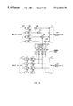
- FIG. 3 is a block diagram showing a configuration of an OFDM transmitting and receiving apparatus according to a first embodiment of the present invention.
- an S/P (Serial-Parallel) converter 101 converts a primary modulated transmitting signal (MOD-S) of one channel to signals of a plurality of channels.
- MOD-S primary modulated transmitting signal
- signals of one channel are converted to signals of four channels.
- Mapping circuits 102 to 105 map the signals of subcarriers A to D subjected to S/P conversion, respectively.
- Multipliers 106 to 109 multiply the mapped signals of subcarriers A to D by signals of predetermined coefficients (hereinafter referred to as coefficient signals).
- An IFFT (Inverse Fast Fourier Transform) circuit 110 provides inverse fast Fourier transform to transmitting signals output from the multipliers 106 to 109 .
- a D/A (Digital/Analog) converter 111 D/A converts an output signal of the IFFT circuit 110 to output a transmitting signal (TR-S).
- An A/D (analog/Digital) converter 151 provides A/D conversion to received signals (RE-S).
- An FFT (Fast Fourier Transform) circuit 152 provides inverse fast Fourier transform to the signals digitally converted.
- Detectors 153 to 156 provide detection processing to the signals of subcarriers A to D output from the FFT circuit 152 , respectively.
- Determination units 157 to 160 provide determination to the signals of subcarriers A to D subjected to detection processing to demodulate these signals.
- a P/S (Paralle-Serial) converter 161 converts the demodulated signals (DEM-S) of the plurality of channels to the signals of one channel.
- the signals of four channels are converted to the signals of one channel.
- a control circuit 162 calculates a coefficient by which the transmitting signals of the respective subcarriers are multiplied, and the calculated coefficient signal is output to multipliers 106 to 109 based on the output signal of the FFT circuit 152 .
- control circuit 162 will explain a detailed configuration of the control circuit 162 with reference to the block diagram of FIG. 4 .
- envelope generators 201 to 204 generate envelopes of the received signals of subcarriers (SUB-C) A to D output from the FFT circuit 152 .
- An averaging circuit 205 calculates an average of output signals of the envelope generators 201 to 204 .
- Dividers 206 to 209 divides the average value output from the averaging circuit 205 by the output signal of each of the envelope generators 201 to 204 so as to calculate each of the coefficient signals of the subcarriers.
- Memories 210 to 213 temporarily store the coefficient signals (COE-S) output from the dividers 206 to 209 , and output them to the multipliers 106 to 109 , respectively.
- the S/P converter 101 parallel converts the transmitting signals, which have been primary modulated, to the number of subcarriers, that is, four subcarriers A to D.
- the transmitting signals of subcarriers A to D are mapped by the mapping circuits 102 to 105 , respectively, and the mapped signals are multiplied by the coefficient signals by the multipliers 106 to 109 , and the resultant signals are output to the IFFT converter 110 .
- the respective signals input to the IFFT converter 110 are subjected to inverse fast Fourier transform, and the resultant signals are converted to analog signals by the D/A converter 111 . Then, the converted signals are amplified; thereafter they are radio transmitted from the antenna.
- the received signals are converted to digital signals by the A/D converter 151 , and the digital signals are subjected to inverse fast Fourier transform by the FFT converter 152 .
- the received signals of subcarriers A to D output from the FFT converter 152 are subjected to detection processing by the detectors 153 to 156 , and the resultant signals are demodulated by binary determination of determining units 157 to 160 , and the demodulated signals are converted to signals of one channel by the P/S converter 161 .
- the envelope generators 201 to 204 generate envelopes of the received signals of subcarriers A to D output from the FFT circuit 152 .
- the averaging circuit 205 calculates an average of the output signals of the envelope generators 201 to 204 .
- the dividers 206 to 209 divide the output signal of each of the envelope generators 201 to 204 by the average value to calculate each of the coefficient signals by which the transmitting signals are multiplied.
- the calculated coefficient signals of subcarriers A to D are temporarily stored in the memories 210 to 213 , thereafter they are output to the multipliers 106 to 109 .
- FIGS. 5A and 5B are views showing one example of a spectrum of the signal transmitted from the OFDM transmitting and receiving apparatus according to the first embodiment.
- FIG. 5A shows a signal spectrum at a signal transmitting time of the base station
- FIG. 5B shows a signal spectrum at a signal receiving time of a partner station.
- the weight is assigned to transmission power every subcarrier such that power can be maintained substantially constant at the time when the signals are received by the partner station based on power of the received signals from the partner station. This makes it possible to improve an error rate characteristic.
- the present apparatus is used in the base station apparatus, and transmission power control is performed. This makes it possible to improve an error rate characteristic of a forward link without increasing a hardware scale of a communication terminal apparatus.
- FIG. 6 is a block diagram showing a configuration of the periphery of the control circuit 162 of the OFDM transmitting and receiving apparatus according to the second embodiment of the present invention.
- the same reference numerals as those of FIG. 4 are added to the portions common to the OFDM transmitting and receiving apparatus of FIG. 4, and the explanation is omitted.
- the OFDM transmitting and receiving apparatus of FIG. 6 adopts a configuration in which connection switches 221 to 224 are added to the control circuit 162 as compared with the OFDM transmitting and receiving apparatus of FIG. 4 .
- the envelope generators 201 to 204 output the generated envelopes to the connection switches 221 to 224 .
- the connection switches 221 to 224 output only final symbols of the signals of subcarriers A to D, which have been output from the envelope generators 201 to 204 , to the averaging circuit 205 and the dividers 206 to 209 based on a timing signal.
- the averaging circuit 205 calculates average value of power in the final symbols of the received signals.
- the dividers 206 to 209 divide the average value of power in the final symbols of the received signals output from the averaging circuit 205 by power of the signals in the final symbols of the received signals, whereby calculating the coefficient signals of the respective subcarriers.
- the calculation of the coefficient signals of subcarriers using power of the final symbols of the received signals makes it possible to reduce an error caused by variations in the link, and to further improve the error rate as compared with the first embodiment.
- FIG. 7 is a block diagram showing a configuration of the periphery of the control circuit 162 of the OFDM transmitting and receiving apparatus according to the third embodiment of the present invention.
- the same reference numerals as those of FIG. 4 are added to the portions common to the OFDM transmitting and receiving apparatus of FIG. 4, and the explanation is omitted.
- the OFDM transmitting and receiving apparatus of FIG. 7 adopts a configuration in which averaging circuits 231 to 234 are added to the control circuit 162 as compared with the OFDM transmitting and receiving apparatus of FIG. 4 .
- the envelope generator 201 to 204 output the generated envelopes to the averaging circuit 231 to 234 .
- the averaging circuits 231 to 234 calculate the average value of the signals of subcarriers A to D output from the envelope generators 201 to 204 based on a timing signal, and output them to the averaging circuit 205 and dividers 206 to 209 .
- the averaging circuit 205 averages the values of the averaging circuits 231 to 234 .
- the dividers 206 to 209 divide the average value of power in the final symbols of the received signals, which have been output from the averaging circuit 205 , by power of the signals output from the averaging circuits 231 to 234 , whereby calculating the coefficient signals of the respective subcarriers.
- the calculation of the coefficient signals of subcarriers using the average value of power of the received signals makes it possible to reduce deterioration in accuracy caused by influence of noise, and to further improve the error rate as compared with the first and second embodiments.
- FIG. 8 is a block diagram showing a configuration of the periphery of the control circuit 162 of the OFDM transmitting and receiving apparatus according to the fourth embodiment of the present invention.
- the same reference numerals as those of FIG. 4 are added to the portions common to the OFDM transmitting and receiving apparatus of FIG. 4, and the explanation is omitted.
- the OFDM transmitting and receiving apparatus of FIG. 8 adopts a configuration in which digital subtracters 241 to 244 , determination units 245 to 248 , and selector switches 249 to 252 are added to the control circuit 162 as compared with the OFDM transmitting and receiving apparatus of FIG. 4 .
- the averaging circuit 205 outputs the calculated average value to the dividers 206 to 208 and the digital subtractors 241 to 244 .
- the digital subtractors 241 to 244 subtract the output signal of the averaging circuit 205 from the output signals of the envelope generators 201 to 204 , and output the subtraction result to the determination units 245 to 248 , respectively.
- the determination units 245 to 248 output coefficient signals stored in the memories 210 to 213 to the multipliers 106 to 109 , respectively. In other cases, the determination units 245 to 248 control the selector switches 249 to 252 to output a coefficient “1.0” to the multipliers 106 to 109 .
- the fourth embodiment can be combined with the second or third embodiment.
- FIG. 9 is a block diagram showing a configuration of the periphery of the control circuit 162 of the OFDM transmitting and receiving apparatus according to the fifth embodiment of the present invention.
- the same reference numerals as those of FIG. 8 are added to the portions common to the OFDM transmitting and receiving apparatus of FIG. 8, and the explanation is omitted.
- the OFDM transmitting and receiving apparatus of FIG. 9 adopts a configuration in which a threshold value (TH) is set in the control circuit 162 and a digital subtracter 261 is added as compared with the OFDM transmitting and receiving apparatus of FIG. 8 .
- TH threshold value
- the averaging circuit 205 outputs the calculated average value to the dividers 206 to 209 and the subtracter 261 .
- the subtracter 261 subtracts a preset threshold value from the output signal of the averaging circuit 205 , and outputs the subtraction result to the digital subtracters 241 to 244 .
- the digital subtracters 241 to 244 subtract the output signal of the subtracter 261 from the envelope generators 201 to 204 , and output the subtraction result to the determination units 245 to 248 , respectively.
- the threshold value is preset, and the transmitting signal of subcarrier wherein reception power is way below the value obtained by subtracting the threshold value from the average value is multiplied by the coefficient.
- the fifth embodiment can be combined with the second or third embodiment.
- FIG.10 is a block diagram showing a configuration of the periphery of the control circuit 162 of the OFDM transmitting and receiving apparatus according to the sixth embodiment of the present invention.
- the same reference numerals as those of FIG. 9 are added to the portions common to the OFDM transmitting and receiving apparatus of FIG. 9, and the explanation is omitted.
- the OFDM transmitting and receiving apparatus of FIG. 10 adopts a configuration in which a threshold value 1, which is used when a link quality is good, is set and a threshold value 2, which is used when the link quality is poor, is set in the control circuit 162 , and a selector switch 271 is added as compared with the OFDM transmitting and receiving apparatus of FIG. 9 .
- the selector switch 271 outputs threshold value 1 to the subtracter 261 when the link quality is good and threshold value 2 thereto when the link quality is poor based on a link quality signal (QUA-S).
- the subtracter 261 subtracts threshold 1 or 2 from the output signal of the averaging circuit 205 , and outputs the subtraction result to the digital subtracters 241 to 244 .
- the threshold value for use in determining whether or not the coefficient signal is multiplied is appropriately changed based on the link quality, and this makes it possible to more improve the error rate characteristic than the fifth embodiment.
- the sixth embodiment can be combined with the second or third embodiment.
- FIG. 11 is a block diagram showing a configuration of the periphery of the control circuit 162 of the OFDM transmitting and receiving apparatus according to the seventh embodiment of the present invention.
- the same reference numerals as those of FIG. 4 are added to the portions common to the OFDM transmitting and receiving apparatus of FIG. 4, and the explanation is omitted.
- the OFDM transmitting and receiving apparatus of FIG. 11 adopts a configuration in which determination units 281 to 284 and selector switches 285 to 288 are added to the control circuit 162 as compared with the OFDM transmitting and receiving apparatus of FIG. 4 .
- the dividers 206 to 209 output the calculated coefficient signals of subcarriers to the memories 210 to 213 and determination units 281 to 284 .
- the determination units 281 to 284 When the coefficient signals of subcarriers are below a predetermined upper limit value (ULV: for example, “2.0”), the determination units 281 to 284 output the coefficient signals stored in the memories 210 to 213 to the multipliers 106 to 109 . When the coefficient signals of subcarriers exceed the predetermined upper limit value, they control the selector switches 285 to 288 such that the upper limit value is output to the multipliers 106 to 109 .
- a predetermined upper limit value for example, “2.0
- the upper limit is provided to the coefficient by which the transmitting signals of subcarriers are multiplied. Whereby, peak power can be suppressed and the capacity of transmission amplifier can be controlled.
- FIG. 12 is a block diagram showing a configuration of the periphery of the control circuit 162 of the OFDM transmitting and receiving apparatus according to the eighth embodiment of the present invention.
- the same reference numerals as those of FIG. 4 are added to the portions common to the OFDM transmitting and receiving apparatus of FIG. 4, and the explanation is omitted.
- the OFDM transmitting and receiving apparatus of FIG. 12 adopts a configuration in which determination units 281 to 284 and selector switches 285 to 288 are added to the control circuit 162 as compared with the OFDM transmitting and receiving apparatus of FIG. 4 .
- the dividers 206 to 209 output the calculated coefficient signals of subcarriers to the memories 210 to 213 and determination units 281 to 284 .
- the determination units 281 to 284 When the coefficient signals of subcarriers are below a predetermined lower limit value (LLV: for example, “0.2”), the determination units 281 to 284 output the coefficient signals stored in the memories 210 to 213 to the multipliers 106 to 109 . When the coefficient signals of subcarriers are below the predetermined lower limit value, they controls the selector switches 285 to 288 such that the lower limit value is output to the multipliers 106 to 109 .
- LUV predetermined lower limit value
- the lower limit is provided to the coefficient by which the transmitting signals of subcarriers are multiplied. This makes it possible to prevent the level difference between the subcarriers to be increased by performing gain control when a time interval between the reverse link and the forward link is large.
- the eighth embodiment can be combined with any one of the second to seventh embodiments.
- FIG. 13 is a block diagram showing a configuration of the periphery of the control circuit 162 of the OFDM transmitting and receiving apparatus according to the ninth embodiment of the present invention.
- the same reference numerals as those of FIG. 4 are added to the portions common to the OFDM transmitting and receiving apparatus of FIG. 4, and the explanation is omitted.
- the OFDM transmitting and receiving apparatus of FIG. 13 adopts a configuration in which connection switches 291 to 294 and selector switches 295 to 298 are added to the control circuit 162 as compared with the OFDM transmitting and receiving apparatus of FIG. 4 .
- the envelope generators 201 to 204 output the generated envelopes to the connection switches 291 to 294 .
- the connection switches 291 to 294 output the signals of subcarriers A to D, which have been output from the envelope generators 201 to 204 , to the averaging circuit 205 and dividers 206 to 209 based on the timing signal only in a case where packets each having important information is mounted thereon are transmitted.
- the selector switches 295 to 298 output the coefficient signals stored in the memories 210 to 213 to the multipliers 106 to 109 based on the timing signal. In other cases, they output the coefficient “1.0” to the multipliers 106 to 109 .
- gain control to multiply the transmitting signals of subcarriers by the efficient is performed only when packets each having important information is mounted thereon are transmitted.
- the forward link is placed in the first half of the frame and the reverse link is placed in the second half, there is no need to reserve the coefficients corresponding to the number of users, and the memory capacity can be suppressed.
- the memories can be shared with the demodulation circuit if the number of coefficients to be reserved is equivalent to one user at the maximum.
- the ninth embodiment may be appropriately combined with any one of the second to eighth embodiments.
- FIG. 14 is a block diagram showing a configuration of the OFDM transmitting and receiving apparatus according to the tenth embodiment of the present invention.
- the same reference numerals as those of FIG. 3 are added to the portions common to the OFDM transmitting and receiving apparatus of FIG. 3, and the explanation is omitted.
- the OFDM transmitting and receiving apparatus of FIG. 14 adopts a configuration in which selector switches 121 to 124 in place of the multipliers 106 to 109 and one bit shift circuits 125 to 128 for doubling amplitude are used.
- the OFDM transmitting and receiving apparatus of FIG. 14 adopts a configuration in which a control circuit 171 for outputting a control signal is used in place of the control circuit 162 for outputting the coefficient signal.
- FIG. 15 is a block diagram showing a configuration of the periphery of the control circuit 171 of the OFDM transmitting and receiving apparatus according to the tenth embodiment of the present invention.
- the same reference numerals as those of FIG. 8 are added to the portions common to the control circuit 162 of the OFDM transmitting and receiving apparatus of FIG. 8, and the explanation is omitted.
- the control circuit 171 of the OFDM transmitting and receiving apparatus shown in FIG. 15 adopts a configuration in which the dividers 206 to 209 , memories 210 to 213 , and selector switches 249 to 252 are deleted, and the control signals of the determination units 245 to 248 are output.
- the control circuit 171 outputs the output signals of the mapping circuits 102 to 105 to the one bit shift circuits 125 to 128 .
- the control circuit 171 controls selector switches 121 to 124 such that the output signals of the mapping circuits 102 to 105 are directly output to the IFFT circuit 110 .
- amplitude is changed by the bit shift circuits and adder-subtracters without using the multipliers, so that the circuit scale can be reduced.
- a plurality of magnification of amplitude such as “2.0”, “1.5”, “1.25”, and the like, which can be implemented by combining the bit shift circuits and the adder-subtracters, is prepared.
- the magnification of amplitude is switched and controlled based on reception power of each subcarrier in order to select magnification appropriately, whereby making it possible to perform precise transmission power control.
- the tenth embodiment can be combined with the second or third embodiment.
- the subtracter 261 is added to subtract a predetermined threshold value from the output signal of the averaging circuit 205 . Then, by use of the obtained value, the determination may be performed.
- the selector switch 271 is added so that the threshold value for use in the determination may be appropriately changed.
- FIG. 16 is a block diagram showing a configuration of the OFDM transmitting and receiving apparatus according to the eleventh embodiment of the present invention.
- the same reference numerals as those of FIG. 3 are added to the portions common to the OFDM transmitting and receiving apparatus of FIG. 3, and the explanation is omitted.
- the OFDM transmitting and receiving apparatus of FIG. 16 adopts a configuration in which connection switches 181 to 184 are added as compared with the OFDM transmitting and receiving apparatus of FIG. 3 .
- connection switches 181 to 184 perform connection and disconnection based on a channel type signal. Then, the connection switches 181 to 184 output only the signal, which relates to a specific channel such as a control channel among the received signals of subcarriers A to D output form the FFT converter 152 , to the control circuit 162 .
- processing for calculating the coefficient of the specific channel is performed in a case where the characteristic is little deteriorated even if the coefficient to be used in performing weighting of amplitude is set to the same value in a plurality of bursts such as a case wherein the variation in the link is slow. Whereby making it possible to reduce average power consumption.
- the eleventh embodiment can be combined with any one of the second to tenth embodiments.
- FIG. 17 is a block diagram showing a configuration of the OFDM transmitting and receiving apparatus according to the twelfth embodiment of the present invention.
- the same reference numerals as those of FIG. 3 are added to the portions common to the OFDM transmitting and receiving apparatus of FIG. 3, and the explanation is omitted.
- the OFDM transmitting and receiving apparatus of FIG. 17 adopts a configuration in which connection switches 191 to 194 are added as compared with the OFDM transmitting and receiving apparatus of FIG. 3 .
- connection switches 191 to 194 perform connection and disconnection based on a timing signal. Then, the connection switches 191 to 194 output only a pilot symbol among the received signals of subcarriers A to D, which have been output form the FFT converter 152 , to the control circuit 162 .
- coefficient can be determined by use of only the pilot symbol. Therefore, even in such a modulation system that information is superimposed on amplitude in addition to phase as in 16QAM, the pilot symbol has generally a low modulation multivalued number, the coefficient is not changed by the modulation signal and deterioration of characteristic can be prevented.
- the twelfth embodiment can be combined with any one of the second to tenth embodiments.
- FIG. 18 is a block diagram showing a configuration of the OFDM transmitting and receiving apparatus according to the thirteenth embodiment of the present invention.
- the same reference numerals as those of FIG. 3 are added to the portions common to the OFDM transmitting and receiving apparatus of FIG. 3, and the explanation is omitted.
- the OFDM transmitting and receiving apparatus of FIG. 18 adopts a configuration in which determination unit 401 and connection switches 411 to 414 are added as compared with the OFDM transmitting and receiving apparatus of FIG. 3 .
- the determination unit 401 compares a link quality signal wherein a quality of link is expressed by a numeral form with a preset threshold value A. Then, the determination unit 401 controls the selector switches 411 to 414 to connect only the switch, which deals with the user wherein the link quality signal exceeds the threshold value A, among these switches. For reference sake, the quality of link can be converted into number by a difference in level between the signals before and after a hard determination in the modulation is performed.
- connection switches 411 to 414 perform connection and disconnection based on control of the determination unit 401 . Then, the connection switches 411 to 414 output only the signal whose link quality is poor among the received signals of subcarriers A to D, which have been output form the FFT converter 152 , to the control circuit 162 .
- the thirteenth embodiment can be combined with any one of the second to twelfth embodiments.
- FIG. 19 is a block diagram showing a configuration of the OFDM transmitting and receiving apparatus according to the fourteenth embodiment of the present invention.
- the same reference numerals as those of FIG. 18 are added to the portions common to the OFDM transmitting and receiving apparatus of FIG. 18, and the explanation is omitted.
- the OFDM transmitting and receiving apparatus of FIG. 19 adopts a configuration in which an averaging circuit 402 is added as compared with the OFDM transmitting and receiving apparatus of FIG. 18 .
- the averaging circuit 402 averages the line quality signals through the plurality of frames, and calculates an average value of the link quality signals.
- the determination unit 401 compares the average value of the link quality signals with the preset threshold value A. Then, the determination unit 401 controls the selector switches 411 to 414 to connect only the switch, which deals with the user wherein the average value of the link quality signals exceeds the threshold value A, among these switches.
- the fourteenth embodiment can be combined with any one of the second to twelfth embodiments.
- FIG. 20 is a block diagram showing a configuration of the OFDM transmitting and receiving apparatus according to the fifteenth embodiment of the present invention.
- the same reference numerals as those of FIG. 18 are added to the portions common to the OFDM transmitting and receiving apparatus of FIG. 18, and the explanation is omitted.
- the OFDM transmitting and receiving apparatus of FIG. 20 adopts a configuration in which a determination unit 403 and an AND circuit 404 are added as compared with the OFDM transmitting and receiving apparatus of FIG. 18 .
- the termination unit 401 compares the link quality signal with the preset threshold value A, and outputs a signal showing a comparison result to the AND circuit 404 .
- the termination unit 403 compares the link quality signal with the preset threshold value B, and outputs a signal showing a comparison result to the AND circuit 404 .
- the threshold value B is higher than the threshold value A.
- the AND circuit 404 controls the selector switches 411 to 414 to connect only the switch, which deals with the user wherein the average value of the link quality signals exceeds the threshold value A and is below the threshold value B, among these switches.
- connection switches 411 to 414 perform connection and disconnection based on control of the AND circuit 404 . Then, the connection switches 411 to 414 output only the signal whose link quality is poor among the received signals of subcarriers A to D excepting one whose link quality is extremely poor, which have been output form the FFT converter 152 , to the control circuit 162 .
- the fifteenth embodiment can be combined with any one of the second to twelfth and fourteenth embodiments.
- FIG. 21 is a block diagram showing a configuration of the OFDM transmitting and receiving apparatus according to the sixteenth embodiment of the present invention.
- the same reference numerals as those of FIG. 18 are added to the portions common to the OFDM transmitting and receiving apparatus of FIG. 18, and the explanation is omitted.
- the OFDM transmitting and receiving apparatus of FIG. 21 adopts a configuration in which a CRC (Cyclic Redundancy Check) circuit 405 , a counter 406 , a determination unit 407 and an AND circuit 408 are added as compared with the OFDM transmitting and receiving apparatus of FIG. 18 .
- CRC Cyclic Redundancy Check
- the termination unit 401 compares the link quality signal with the preset threshold value A, and outputs a signal showing a comparison result to the AND circuit 408 .
- the CRC circuit 405 checks correctness and error of a check bit of the signal output from the P/S converter 161 . Then, the CRC circuit 405 outputs a pulse signal to the counter 406 when the check bit is error.
- the counter 406 counts the number of pulse signals output from the CRC circuit 405 over a predetermined period, for example, 10 frames, and outputs a counted value to the determination unit 407 .
- the determination unit 407 compares the counted value output from the counter 406 with a preset value C, and outputs a signal showing a comparison result to the AND circuit 408 .
- the AND circuit 408 controls the selector switches 411 to 414 to connect only the switch, which deals with the user wherein the link quality signal is below the threshold value A, among these switches when the counted value is below the threshold value C.
- connection switches 411 to 414 perform connection and disconnection based on control of the AND circuit 408 . Then, the connection switches 411 to 414 output only the signal whose link quality is poor among the received signals of subcarriers A to D, which have been output form the FFT converter 152 , to the control circuit 162 .
- sixteenth embodiment can be combined with any one of the second to twelfth, fourteenth and fifteenth embodiments.
- FIG. 22 is a block diagram showing a configuration of the OFDM transmitting and receiving apparatus according to the seventeenth embodiment of the present invention.
- the same reference numerals as those of FIG. 3 are added to the portions common to the OFDM transmitting and receiving apparatus of FIG. 3, and the explanation is omitted.
- the OFDM transmitting and receiving apparatus of FIG. 22 adopts a configuration in which a memory 421 , a determination unit 422 , and selector switches 431 to 434 are added as compared with the OFDM transmitting and receiving apparatus of FIG. 3 .
- the memory 421 temporarily stores the coefficients output from the control circuit 162 . Then, when a coefficient is newly input, the coefficients stored are output, thereby updating the coefficient.
- the determination unit 422 calculates a coefficient difference that is a difference between the coefficient output from the control circuit 162 this time and the coefficient previously output from the memory 421 . Then, the determination unit 422 compares the coefficient difference and a preset threshold value D. After that, the determination unit 422 controls the selector switches 431 to 434 in order to output the coefficient output from the control circuit 162 in a case where the coefficient difference is below the threshold value D, and to output a coefficient of “1.0” to the multipliers 106 to 109 in other cases.
- the selector switches 431 to 434 output the coefficient output from the control circuit 162 or “1.0” to the multipliers 106 to 109 .
- the seventeenth embodiment can be combined with any one of the second to sixteenth embodiments.
- An eighteenth embodiment is one wherein processing for assigning a weight to transmission power every subcarrier and processing for performing selection diversity by a plurality of antenna branches are combined to each other.
- the explanation is given on the assumption that the number of transmission and reception branches is two (BR 1 and BR 2 ).
- FIG. 23 is a block diagram showing a configuration of the OFDM transmitting and receiving apparatus according to the eighteenth embodiment of the present invention.
- the same reference numerals as those of FIG. 3 are added to the portions common to the OFDM transmitting and receiving apparatus of FIG. 3, and the explanation is omitted.
- the OFDM transmitting and receiving apparatus of FIG. 23 adopts a configuration in which selector switches 521 to 524 , IFFT circuit 510 , and D/A converter 511 are added to the transmitting side and A/D converter 551 , FFT circuit 552 , and selector switches 571 to 574 are added to the receiving side.
- the OFDM transmitting and receiving apparatus of FIG. 23 adopts a configuration in which a control circuit 562 for outputting a control signal and a coefficient signal is used in place of the control circuit 162 for outputting the coefficient signal.
- the selector switches 521 to 524 switch the transmission branch for mapped signals of subcarriers based on the control signal, respectively.
- the IFFT circuit 510 provides inverse fast Fourier transform to the input transmitting signal, similar to the IFFT circuit 110 .
- the D/A converter 511 D/A Digital/Analog converts the output signal of IFFT circuit 510 so as to output transmitting signal of branch 2 , similar to the D/A converter 111 .
- the A/D converter 551 D/A (Digital/Analog) converts the received signal of branch 2 , similar to the A/D converter 151 .
- the FFT circuit 552 provides inverse fast Fourier transform to the signal of branch 2 converted to the digital signal, similar to the FFT circuit 152 .
- the selector switches 571 to 574 output the output signal of any one of the FFT circuit 152 and FFT circuit 552 to detectors 153 to 156 every subcarrier based on the control signal.
- the control circuit 562 calculates the coefficient by which the transmitting signal of each subcarrier is multiplied, and selects a transmission branch based on the output signals of FFT circuit 152 and FFT circuit 552 . Then, the coefficient signal is output to the multipliers 106 to 109 , and the control signal is output to the selector switches 521 to 524 and the selector switches 571 to 574 .
- control circuit 562 will be explained with reference to the block diagram of FIG. 24 .
- the same reference numerals as those of FIG. 4 are added to the portions common to the control circuit 162 of the OFDM transmitting and receiving apparatus of FIG. 4, and the explanation is omitted.
- the control circuit 562 of the OFDM transmitting and receiving apparatus of FIG. 24 adopts a configuration in which digital subtracters 611 to 614 , determination units 615 to 618 , and selector switches 619 to 622 are added as compared with the control circuit 162 of the OFDM transmitting and receiving apparatus of FIG. 4 .
- the digital subtracters 611 to 614 subtract the output signals of the envelope generators 601 to 604 from the output signals of the envelope generators 201 to 204 , respectively, and output the subtraction results to the determination units 615 to 619 , respectively.
- the determination units 615 to 619 determine that a branch suitable for the transmitting signal of subcarrier A is branch 1 . In other cases, they determine that a branch suitable for the transmitting signal of subcarrier A is branch 2 . Then, a control signal (CON-S) on which the determination result is mounted is output to the selector switches 619 to 622 , selector switches 521 to 524 , and selector switches 571 to 574 .
- CON-S control signal
- the selector switches 619 to 622 output the output signals of any one of the envelope generators 201 to 204 and the envelope generator 601 to 604 to the averaging circuit 205 and the dividers 206 to 209 , respectively, based on the control signals output from the determination units 615 to 619 .
- processing for assigning a weight to transmission power every subcarrier and processing for performing transmission diversity are combined to each other. This makes it possible to dramatically improve the error rate characteristic.
- the use of the present apparatus in the base station apparatus makes it possible to improve the error rate characteristic of the forward link without increasing the hardware scale of the communication terminal apparatus.
- Gain control is provided to the transmission diversity. so that a drop in reception level due to phasing can be largely reduced as compared with the case of the single branch. This makes it possible to considerably lessen the gain control value and to largely decrease peak power.
- provision of gain control to the transmission diversity makes it possible to reduce transmission power corresponding to the amount of subcarriers, which have not been transmitted, as compared with the case of the single branch.
- the explanation was given on the assumption that the number of transmission and reception branches was two.
- the present invention does not limit the number of subcarriers, and the number of transmission and reception branches. Furthermore, it is possible to use the selection diversity in only the receiving side.
- FIG. 25 is a block diagram showing a configuration of the OFDM transmitting and receiving apparatus according to the nineteenth embodiment of the present invention.
- the same reference numerals as those of FIG. 23 are added to the portions common to the OFDM transmitting and receiving apparatus of FIG. 23, and the explanation is omitted.
- the OFDM transmitting and receiving apparatus of FIG. 25 adopts a configuration in which a P/S converter 701 , a counter 702 , a determination unit 703 , and selector switches 711 to 714 are added.
- the P/S converter 701 converts a control signal for selecting a transmission branch output from the control circuit 562 in series, and outputs it to the counter 702 .
- the counter 702 counts the number of selected subcarriers every transmission branch based on the control signal output from the P/S converter 701 , and outputs the counted value to the determination unit 703 .
- the determination unit 703 compares a maximum value of the counted value output from the counter 702 with a preset threshold value E. In a case where the maximum value of the counted value exceeds the threshold value E, the determination unit 703 controls the selectors switches 711 to 714 such that the subcarrier transmitted from the corresponding branch is multiplied by coefficient “1.0”, and the other subcarriers are multiplied by the coefficient output from the control circuit 562 .
- the selector switches 711 to 714 output the coefficient output from the control circuit 562 or coefficient “1.0” to the multipliers 106 to 109 based on control of the determination unit 703 .
- the possibility that the number of subcarriers to be transmitted from a specific branch will be greatly increased is considerably low.
- the error rate is little deteriorated even if no gain control is performed.
- no gain control is performed as in this embodiment. This makes it possible to improve both the error rate characteristic and the reduction in peak power.
- FIG. 26 is a block diagram showing a configuration of the OFDM transmitting and receiving apparatus according to the twentieth embodiment of the present invention.
- the same reference numerals as those of FIG. 24 are added to the portions common to the OFDM transmitting and receiving apparatus of FIG. 24, and the explanation is omitted.
- the OFDM transmitting and receiving apparatus of FIG. 26 adopts a configuration in which a P/S converter 631 , a counter 632 , a determination unit 633 , a determination unit 635 , and selector switches 636 to 639 are added to the control circuit 562 .
- the P/S converter 631 series-converts a control signal on which a determination result output from the determination units 615 to 618 is mounted, and outputs it to the counter 632 .
- the counter 632 counts the number of subcarriers to be transmitted every transmission branch based on the control signal output from the P/S converter 631 , and outputs the counted value to the determination unit 633 .
- the determination unit 633 compares a maximum value of the counted value output from the counter 632 with a preset threshold value F.
- the determination unit 633 controls the selector switch 634 to select an upper limit value A (for example, “2.0”) in a case where the maximum value of the counted value is below the threshold value F, and to select an upper limit B (for example, “1.5”) in other cases. In this case, suppose that the upper limit value A is higher than the upper limit value B.
- the selector switch 634 outputs the upper limit value A or the upper limit value B to the determination unit 635 and the selector switches 636 to 639 based on control of the determination unit 633 .
- the determination unit 635 controls the selector switches 635 to 639 such that the coefficient signals stored in the memories 210 to 213 are output to the multipliers 106 to 109 if the coefficient signals of the respective subcarriers are less than the upper limit value output from the selector switch 634 , and the upper limit value is output to the multipliers 106 to 109 if they exceed the upper limit value.
- the upper limit value of the coefficient by which the transmitting signal is multiplied is changed by the number of subcarriers to be transmitted from the specific branch. This makes it possible to reduce peak power as maintaining the error rate characteristic as compared with the case in which the upper limit value is fixed.
- FIG. 27 is a block diagram showing a configuration of the OFDM transmitting and receiving apparatus according to the twenty-first embodiment of the present invention.
- the same reference numerals as those of FIG. 23 are added to the portions common to the OFDM transmitting and receiving apparatus of FIG. 23, and the explanation is omitted.
- the OFDM transmitting and receiving apparatus of FIG. 27 adopts a configuration in which the selector switches 571 to 574 are deleted from the receiving side and detectors 553 to 556 , and combining circuits 581 to 584 are added thereto.
- the FFT circuit 152 provides fast Fourier transform to the signal of the branch 1 , which has been converted to the digital signal, and outputs the received signals of subcarriers A to D to the detectors 153 to 156 .
- the FFT circuit 552 provides fast Fourier transform to the signal of the branch 2 , which has been converted to the digital signal, and outputs the received signals of subcarriers A to D to the detectors 553 to 556 .
- the detectors 153 to 156 provide detection processing to the signals of subcarriers A to D output from the FFT circuit 152 , respectively.
- the detectors 553 to 556 provide detection processing to the signals of subcarriers A to D output from the FFT circuit 552 , respectively.
- the combining circuits 581 to 584 combine the signals of subcarriers A to D, which have bee detected by the detectors 153 to 156 and the detectors 553 to 556 , respectively.
- the determination units 157 to 160 provide determination to the combined signals of subcarriers A to D, respectively, and demodulate them.
- the error rate characteristic can be improved by performing combination diversity every subcarrier at the receiving side.
- the error rate of the reverse link can be improved without performing gain control at the mobile station side. This eliminates the need for increasing the hardware scale of the mobile station.
- FIG. 28 is a block diagram showing a configuration of a main part of the OFDM transmitting and receiving apparatus according to the twenty-second embodiment.
- FIG. 28 shows only the part relating to the signal of the subcarrier A at the receiving side.
- the same reference numerals as those of FIGS. 23 and 24 are added to the portions common to the OFDM transmitting and receiving apparatus of FIGS. 23 and 24, and the explanation is omitted.
- the OFDM transmitting and receiving apparatus of FIG. 28 adopts a configuration in which multipliers 591 , 592 , and an adder 593 are used in place of the combining circuit 581 , and an averaging circuit 301 and dividers 302 and 303 are added to the control circuit 562 .
- the averaging circuit 301 calculates an average value of the output signal of the envelope generator 201 and that of the envelope generator 601 .
- the divider 302 divides the output signal of the envelope generator 201 by the average value output from the averaging circuit 301 , so that a weighting factor of the subcarrier A branch 1 is calculated.
- the divider 303 divides the output signal of the envelope generator 601 by the average value output from the averaging circuit 301 , so that a weighting factor of the subcarrier A branch 2 is calculated.
- the multiplier 591 multiplies the signal of the subcarrier A branch 1 detected by the detector 153 by the weighting factor of the subcarrier A branch 1 .
- the multiplier 592 multiplies the signal of the subcarrier A branch 2 detected by the detector 553 by the weighting factor of the subcarrier A branch 2 .
- the adder 593 adds the weighted signals output from the multipliers 591 and 592 , and outputs the signal of branch A to the determination unit 157 .
- the error rate characteristic can be further improved as compared with the eighteenth embodiment.
- the error rate characteristic can be improved.
Priority Applications (1)
| Application Number | Priority Date | Filing Date | Title |
|---|---|---|---|
| US09/984,944 US6747945B2 (en) | 1998-11-06 | 2001-10-31 | OFDM transmitting and receiving apparatus and OFDM transmitting and receiving method |
Applications Claiming Priority (7)
| Application Number | Priority Date | Filing Date | Title |
|---|---|---|---|
| JP31641498 | 1998-11-06 | ||
| JP10-316414 | 1998-11-06 | ||
| JP11-070814 | 1999-03-16 | ||
| JP7081499 | 1999-03-16 | ||
| JP11-101733 | 1999-04-08 | ||
| JP10173399A JP4287536B2 (ja) | 1998-11-06 | 1999-04-08 | Ofdm送受信装置及びofdm送受信方法 |
| PCT/JP1999/006126 WO2000028687A1 (fr) | 1998-11-06 | 1999-11-04 | Dispositif emetteur/recepteur a multiplexage frequentiel optique et procede correspondant |
Related Parent Applications (1)
| Application Number | Title | Priority Date | Filing Date |
|---|---|---|---|
| PCT/JP1999/006126 A-371-Of-International WO2000028687A1 (fr) | 1998-11-06 | 1999-11-04 | Dispositif emetteur/recepteur a multiplexage frequentiel optique et procede correspondant |
Related Child Applications (1)
| Application Number | Title | Priority Date | Filing Date |
|---|---|---|---|
| US09/984,944 Continuation US6747945B2 (en) | 1998-11-06 | 2001-10-31 | OFDM transmitting and receiving apparatus and OFDM transmitting and receiving method |
Publications (1)
| Publication Number | Publication Date |
|---|---|
| US6345036B1 true US6345036B1 (en) | 2002-02-05 |
Family
ID=27300449
Family Applications (2)
| Application Number | Title | Priority Date | Filing Date |
|---|---|---|---|
| US09/582,613 Expired - Lifetime US6345036B1 (en) | 1998-11-06 | 1999-11-04 | OFDM transmitting/receiving device and method |
| US09/984,944 Expired - Fee Related US6747945B2 (en) | 1998-11-06 | 2001-10-31 | OFDM transmitting and receiving apparatus and OFDM transmitting and receiving method |
Family Applications After (1)
| Application Number | Title | Priority Date | Filing Date |
|---|---|---|---|
| US09/984,944 Expired - Fee Related US6747945B2 (en) | 1998-11-06 | 2001-10-31 | OFDM transmitting and receiving apparatus and OFDM transmitting and receiving method |
Country Status (10)
| Country | Link |
|---|---|
| US (2) | US6345036B1 (no) |
| EP (1) | EP1043857A4 (no) |
| JP (1) | JP4287536B2 (no) |
| KR (1) | KR100396098B1 (no) |
| CN (1) | CN1243422C (no) |
| AU (1) | AU1076300A (no) |
| CA (1) | CA2316904C (no) |
| IL (1) | IL137057A (no) |
| NO (1) | NO331646B1 (no) |
| WO (1) | WO2000028687A1 (no) |
Cited By (28)
| Publication number | Priority date | Publication date | Assignee | Title |
|---|---|---|---|---|
| US20020027875A1 (en) * | 1998-11-06 | 2002-03-07 | Hiroaki Sudo | OFDM transmitting and receiving apparatus and OFDM transmitting and receiving method |
| WO2002071637A1 (en) * | 2001-03-06 | 2002-09-12 | Magis Networks, Inc. | Methods and apparatus for diversity antenna branch selection |
| US20020136190A1 (en) * | 2001-03-26 | 2002-09-26 | Yoshiyuki Hata | Band-division demodulation method and OFDM receiver |
| US20030020651A1 (en) * | 2001-04-27 | 2003-01-30 | Crilly William J. | Wireless packet switched communication systems and networks using adaptively steered antenna arrays |
| US20030235255A1 (en) * | 2002-06-24 | 2003-12-25 | Ketchum John W. | Signal processing with channel eigenmode decomposition and channel inversion for MIMO systems |
| US20040082356A1 (en) * | 2002-10-25 | 2004-04-29 | Walton J. Rodney | MIMO WLAN system |
| US20040085939A1 (en) * | 2002-10-25 | 2004-05-06 | Wallace Mark S. | Channel calibration for a time division duplexed communication system |
| US20040120411A1 (en) * | 2002-10-25 | 2004-06-24 | Walton Jay Rodney | Closed-loop rate control for a multi-channel communication system |
| US20040127245A1 (en) * | 2002-12-30 | 2004-07-01 | Sadri Ali S. | System and method for intelligent transmitted power control scheme |
| US20040137863A1 (en) * | 2002-10-25 | 2004-07-15 | Walton J. Rodney | Data detection and demodulation for wireless communication systems |
| US20040136349A1 (en) * | 2002-10-25 | 2004-07-15 | Walton J. Rodney | MIMO system with multiple spatial multiplexing modes |
| US20040156328A1 (en) * | 2002-10-25 | 2004-08-12 | Walton J. Rodney | Random access for wireless multiple-access communication systems |
| US20040179627A1 (en) * | 2002-10-25 | 2004-09-16 | Ketchum John W. | Pilots for MIMO communication systems |
| US20040208232A1 (en) * | 2001-11-26 | 2004-10-21 | Hiroaki Sudo | Radio transmission apparatus and radio transmission method |
| US20050120097A1 (en) * | 2003-12-01 | 2005-06-02 | Walton J. R. | Method and apparatus for providing an efficient control channel structure in a wireless communication system |
| US20050128953A1 (en) * | 2002-10-25 | 2005-06-16 | Wallace Mark S. | Channel calibration for a time division duplexed communication system |
| WO2005064820A1 (en) * | 2003-12-27 | 2005-07-14 | Electronics And Telecommunications Research Institute | An apparatus for adaptive resource allocation for multi-channel communication system, and a method thereof |
| US20060039275A1 (en) * | 2002-10-25 | 2006-02-23 | Walton J R | Transmit diversity processing for a multi-antenna communication system |
| US20060285605A1 (en) * | 2005-06-16 | 2006-12-21 | Qualcomm Incorporated | Coding and modulation for multiple data streams in a communication system |
| US20070217528A1 (en) * | 2004-08-05 | 2007-09-20 | Matsushita Electric Industrial Co.,Ltd | Data transmission device, radio reception device, radio transmission method, and radio reception method |
| US20070258509A1 (en) * | 2005-01-18 | 2007-11-08 | Akira Ito | Transmission method and transmission apparatus in an OFDM-CDMA communication system |
| US20080311863A1 (en) * | 2004-07-30 | 2008-12-18 | Matsushita Electric Industrial Co., Ltd. | Radio Communication Device and Radio Communication Method |
| US20100139149A1 (en) * | 2008-12-06 | 2010-06-10 | Lawrence William Carignan | Fish Strike Indicator |
| US8194770B2 (en) | 2002-08-27 | 2012-06-05 | Qualcomm Incorporated | Coded MIMO systems with selective channel inversion applied per eigenmode |
| US8203978B2 (en) | 2002-10-25 | 2012-06-19 | Qualcomm Incorporated | Multi-mode terminal in a wireless MIMO system |
| US8855226B2 (en) | 2005-05-12 | 2014-10-07 | Qualcomm Incorporated | Rate selection with margin sharing |
| US9154274B2 (en) | 2002-10-25 | 2015-10-06 | Qualcomm Incorporated | OFDM communication system with multiple OFDM symbol sizes |
| US9551785B1 (en) | 1999-04-07 | 2017-01-24 | James L. Geer | Method and apparatus for the detection of objects using electromagnetic wave attenuation patterns |
Families Citing this family (42)
| Publication number | Priority date | Publication date | Assignee | Title |
|---|---|---|---|---|
| AU774602B2 (en) * | 1998-12-23 | 2004-07-01 | Nokia Inc. | A unified routing scheme for ad-hoc internetworking |
| EP1176750A1 (en) * | 2000-07-25 | 2002-01-30 | Telefonaktiebolaget L M Ericsson (Publ) | Link quality determination of a transmission link in an OFDM transmission system |
| JP2002064461A (ja) * | 2000-08-18 | 2002-02-28 | Mitsubishi Electric Corp | 通信装置および通信方法 |
| JP2002217858A (ja) * | 2001-01-19 | 2002-08-02 | Kddi Research & Development Laboratories Inc | 振幅補正装置 |
| WO2002063341A1 (en) * | 2001-02-02 | 2002-08-15 | Dbi Corporation | Downhole telemetry and control system |
| JP2002280935A (ja) * | 2001-03-19 | 2002-09-27 | Sumitomo Electric Ind Ltd | 電力線搬送におけるマルチキャリア通信装置及び通信方法 |
| KR100510434B1 (ko) | 2001-04-09 | 2005-08-26 | 니폰덴신뎅와 가부시키가이샤 | Ofdm신호전달 시스템, ofdm신호 송신장치 및ofdm신호 수신장치 |
| ES2187274B1 (es) * | 2001-05-17 | 2004-08-16 | Diseño De Sistemas En Silicio, S.A. | Sistema de control automatico de ganancia para sistema de transmision digital ofdm multiusuario sobre red electrica. |
| JP4496673B2 (ja) * | 2001-06-07 | 2010-07-07 | 株式会社デンソー | Ofdm方式の送受信機 |
| JP2002374190A (ja) * | 2001-06-15 | 2002-12-26 | Matsushita Electric Ind Co Ltd | 電力線通信装置および電力線通信システム |
| CA2458268C (en) | 2001-08-28 | 2007-10-02 | Ntt Docomo, Inc. | Multi-carrier cdma transmission system, transmitting apparatus and receiving apparatus used in this system, and multi-carrier cdma transmission method |
| KR100754621B1 (ko) * | 2001-11-09 | 2007-09-05 | 삼성전자주식회사 | 직교주파수분할다중화 방식의 이동통신시스템에서피크전력 대 평균전력의 감소장치 및 방법 |
| JP2003174370A (ja) | 2001-12-05 | 2003-06-20 | Nec Corp | 非線形補償回路と基地局装置および送信電力クリップ方法 |
| CA2415170C (en) * | 2001-12-28 | 2008-07-15 | Ntt Docomo, Inc. | Receiver, transmitter, communication system, and method of communication |
| EP1467508B1 (en) * | 2002-01-10 | 2011-05-11 | Fujitsu Limited | Pilot multiplex method in ofdm system and ofdm receiving method |
| KR100824375B1 (ko) * | 2002-05-24 | 2008-04-23 | 삼성전자주식회사 | Ofdm 수신기 및 그의 신호처리방법 |
| KR100824367B1 (ko) * | 2002-05-24 | 2008-04-22 | 삼성전자주식회사 | Ofdm 송신기 및 그의 신호처리방법 |
| KR100824369B1 (ko) * | 2002-05-28 | 2008-04-22 | 삼성전자주식회사 | 오에프디엠 송신기 및 그의 ofdm 심볼에 보호구간삽입방법 |
| KR100827159B1 (ko) * | 2002-05-31 | 2008-05-02 | 삼성전자주식회사 | 오에프디엠 통신 시스템에서 오에프디엠 심볼을 위한보호구간 삽입/추출 장치 및 방법 |
| TWI271070B (en) | 2002-07-08 | 2007-01-11 | Texas Instruments Inc | Shaped PSD design for DSL systems |
| US6940917B2 (en) * | 2002-08-27 | 2005-09-06 | Qualcomm, Incorporated | Beam-steering and beam-forming for wideband MIMO/MISO systems |
| KR100532422B1 (ko) * | 2003-02-28 | 2005-11-30 | 삼성전자주식회사 | 동일 심볼을 다수의 채널에 중복적으로 전송하여 통신거리를 확장시킨 무선 랜 시스템의 직교 주파수 분할다중화 송수신 장치 및 그 송수신 방법 |
| EP1499059B1 (en) * | 2003-07-18 | 2011-07-06 | Motorola Mobility, Inc. | Method and device for determining the link quality in an OFDM network |
| WO2005029803A2 (en) | 2003-09-19 | 2005-03-31 | Matsushita Electric Industrial Co., Ltd. | Multicarrier communication method, system and apparatus |
| US7505522B1 (en) * | 2003-10-06 | 2009-03-17 | Staccato Communications, Inc. | Spectral shaping in multiband OFDM transmitter with clipping |
| US7519123B1 (en) | 2004-04-08 | 2009-04-14 | Staccato Communications, Inc. | Spectral shaping for multiband OFDM transmitters with time spreading |
| JP4429795B2 (ja) * | 2004-05-06 | 2010-03-10 | 株式会社エヌ・ティ・ティ・ドコモ | 無線通信システム、無線送信機及び無線受信機 |
| CN101048960B (zh) | 2004-10-29 | 2013-01-09 | 夏普株式会社 | 通信方法和无线发射机 |
| CN102307379B (zh) * | 2005-01-18 | 2015-06-17 | 夏普株式会社 | 无线通信装置、便携式终端以及无线通信方法 |
| US7954032B2 (en) | 2005-06-17 | 2011-05-31 | Samsung Electronics Co., Ltd. | Apparatus and method for transmitting/receiving broadcast data in a mobile communication system |
| KR101003087B1 (ko) * | 2005-06-17 | 2010-12-21 | 삼성전자주식회사 | 이동통신 시스템에서 방송 데이터의 송수신 장치 및 방법 |
| JP4229936B2 (ja) | 2005-09-26 | 2009-02-25 | 京セラ株式会社 | 無線通信方法及び無線通信装置 |
| JP4766310B2 (ja) * | 2005-09-27 | 2011-09-07 | 住友電気工業株式会社 | 送信装置及び送信方法 |
| KR100746998B1 (ko) * | 2005-12-09 | 2007-08-07 | 한국전자통신연구원 | 직교 주파수 분할 다중 시스템에서 송신 전력 제어 장치 및방법 |
| JP4752523B2 (ja) * | 2006-01-26 | 2011-08-17 | ソニー株式会社 | 無線通信装置及び方法 |
| KR100934656B1 (ko) | 2006-02-06 | 2009-12-31 | 엘지전자 주식회사 | 다중 반송파 시스템에서의 무선 자원 할당 방법 |
| JP4714635B2 (ja) * | 2006-04-27 | 2011-06-29 | 京セラ株式会社 | マルチキャリア受信装置及びマルチキャリア受信装置の制御方法 |
| JP2008289046A (ja) * | 2007-05-21 | 2008-11-27 | Kyocera Corp | Ofdma受信装置およびofdma受信方法 |
| WO2008157724A1 (en) * | 2007-06-19 | 2008-12-24 | The Trustees Of Columbia University In The City Of New York | Methods and systems for providing feedback for beamforming and power control |
| RU2460216C2 (ru) * | 2007-07-06 | 2012-08-27 | Телефонактиеболагет Лм Эрикссон (Пабл) | Установка максимальной мощности в базовой станции системы мобильной связи, имеющей множество антенн |
| JP2009118388A (ja) * | 2007-11-09 | 2009-05-28 | Nec Electronics Corp | 受信装置 |
| JP5407562B2 (ja) | 2009-06-03 | 2014-02-05 | 富士通セミコンダクター株式会社 | 送信装置 |
Citations (12)
| Publication number | Priority date | Publication date | Assignee | Title |
|---|---|---|---|---|
| JPH03254236A (ja) | 1990-03-02 | 1991-11-13 | Fujitsu Ltd | マイクロ波多重無線送信装置 |
| JPH05268178A (ja) | 1992-03-19 | 1993-10-15 | Fujitsu Ltd | 送信電力制御方式 |
| US5307376A (en) * | 1991-01-17 | 1994-04-26 | France Telecom | Device for the coherent demodulation of time-frequency interlaced digital data, with estimation of the frequency response of the transmission channel and threshold, and corresponsing transmitter |
| EP0600547A1 (en) | 1992-12-01 | 1994-06-08 | Koninklijke Philips Electronics N.V. | Sub-band diversity transmission system |
| US5357502A (en) * | 1990-02-06 | 1994-10-18 | France Telecom And Telediffusion De France Sa | Device for the reception of digital data time frequency interlacing, notably for radio broadcasting at high bit rate towards mobile receivers with nyquist temporal window |
| JPH09215051A (ja) | 1995-11-28 | 1997-08-15 | Sanyo Electric Co Ltd | 移動体通信システムの基地局 |
| JPH10107714A (ja) | 1996-08-06 | 1998-04-24 | Toshiba Corp | 受信装置 |
| US5867532A (en) * | 1995-03-31 | 1999-02-02 | Sony Corporation | Data reception apparatus, data transmission apparatus and method thereof |
| JPH11205205A (ja) | 1998-01-09 | 1999-07-30 | Nippon Telegr & Teleph Corp <Ntt> | マルチキャリア信号伝送装置 |
| JPH11289312A (ja) | 1998-04-01 | 1999-10-19 | Toshiba Tec Corp | マルチキャリア無線通信装置 |
| US6009073A (en) * | 1995-09-25 | 1999-12-28 | Victor Company Of Japan, Ltd. | Method for transmitting an orthogonal frequency division multiplex signal, apparatus for transmitting the signal and apparatus for receiving the signal |
| US6125103A (en) * | 1996-09-04 | 2000-09-26 | Telefonaktiebolaget Lm Ericsson | Method and device for reducing the crest factor in digital transmission procedures |
Family Cites Families (16)
| Publication number | Priority date | Publication date | Assignee | Title |
|---|---|---|---|---|
| JP2700746B2 (ja) * | 1992-11-20 | 1998-01-21 | エヌ・ティ・ティ移動通信網株式会社 | 周波数ホッピング通信方式 |
| JP2734953B2 (ja) * | 1993-12-16 | 1998-04-02 | 日本電気株式会社 | Cdma受信装置 |
| JP3124717B2 (ja) * | 1995-01-10 | 2001-01-15 | 松下電器産業株式会社 | 直交周波数分割多重信号の伝送方法およびその受信装置 |
| JPH08331095A (ja) * | 1995-05-31 | 1996-12-13 | Sony Corp | 通信システム |
| US5960039A (en) * | 1996-04-10 | 1999-09-28 | Lucent Technologies Inc. | Methods and apparatus for high data rate transmission in narrowband mobile radio channels |
| JP2785804B2 (ja) * | 1996-05-30 | 1998-08-13 | 日本電気株式会社 | 移動通信システム |
| CA2183140C (en) * | 1996-08-12 | 2001-11-20 | Grant Mcgibney | Ofdm timing and frequency recovery system |
| JPH1065609A (ja) * | 1996-08-23 | 1998-03-06 | Sony Corp | 通信方法、基地局及び端末装置 |
| JP2820143B2 (ja) * | 1997-01-17 | 1998-11-05 | 日本電気株式会社 | 自動周波数制御方式 |
| JP3537988B2 (ja) * | 1997-03-25 | 2004-06-14 | 松下電器産業株式会社 | 無線送信装置 |
| JP3274388B2 (ja) * | 1997-07-25 | 2002-04-15 | 株式会社東芝 | Rake受信機とこのrake受信機を備えたスぺクトラム拡散通信装置 |
| JP3913879B2 (ja) * | 1998-02-03 | 2007-05-09 | 富士通株式会社 | 移動速度に基づく通信制御装置および方法 |
| KR100379492B1 (ko) * | 1998-06-08 | 2003-05-17 | 엘지전자 주식회사 | 이동 통신 시스템의 전력 제어 장치 |
| ATE248465T1 (de) * | 1998-06-29 | 2003-09-15 | Nokia Corp | Leistungsregelung in einer mehrfachträger- funksendeeinrichtung |
| US6317470B1 (en) * | 1998-09-15 | 2001-11-13 | Ibiquity Digital Corporation | Adaptive weighting method for orthogonal frequency division multiplexed soft symbols using channel state information estimates |
| JP4287536B2 (ja) * | 1998-11-06 | 2009-07-01 | パナソニック株式会社 | Ofdm送受信装置及びofdm送受信方法 |
-
1999
- 1999-04-08 JP JP10173399A patent/JP4287536B2/ja not_active Expired - Fee Related
- 1999-11-04 AU AU10763/00A patent/AU1076300A/en not_active Abandoned
- 1999-11-04 CN CNB998019909A patent/CN1243422C/zh not_active Expired - Fee Related
- 1999-11-04 EP EP99954362A patent/EP1043857A4/en not_active Withdrawn
- 1999-11-04 WO PCT/JP1999/006126 patent/WO2000028687A1/ja not_active Application Discontinuation
- 1999-11-04 US US09/582,613 patent/US6345036B1/en not_active Expired - Lifetime
- 1999-11-04 KR KR10-2000-7007504A patent/KR100396098B1/ko not_active IP Right Cessation
- 1999-11-04 CA CA002316904A patent/CA2316904C/en not_active Expired - Fee Related
- 1999-11-04 IL IL13705799A patent/IL137057A/en not_active IP Right Cessation
-
2000
- 2000-07-05 NO NO20003475A patent/NO331646B1/no not_active IP Right Cessation
-
2001
- 2001-10-31 US US09/984,944 patent/US6747945B2/en not_active Expired - Fee Related
Patent Citations (12)
| Publication number | Priority date | Publication date | Assignee | Title |
|---|---|---|---|---|
| US5357502A (en) * | 1990-02-06 | 1994-10-18 | France Telecom And Telediffusion De France Sa | Device for the reception of digital data time frequency interlacing, notably for radio broadcasting at high bit rate towards mobile receivers with nyquist temporal window |
| JPH03254236A (ja) | 1990-03-02 | 1991-11-13 | Fujitsu Ltd | マイクロ波多重無線送信装置 |
| US5307376A (en) * | 1991-01-17 | 1994-04-26 | France Telecom | Device for the coherent demodulation of time-frequency interlaced digital data, with estimation of the frequency response of the transmission channel and threshold, and corresponsing transmitter |
| JPH05268178A (ja) | 1992-03-19 | 1993-10-15 | Fujitsu Ltd | 送信電力制御方式 |
| EP0600547A1 (en) | 1992-12-01 | 1994-06-08 | Koninklijke Philips Electronics N.V. | Sub-band diversity transmission system |
| US5867532A (en) * | 1995-03-31 | 1999-02-02 | Sony Corporation | Data reception apparatus, data transmission apparatus and method thereof |
| US6009073A (en) * | 1995-09-25 | 1999-12-28 | Victor Company Of Japan, Ltd. | Method for transmitting an orthogonal frequency division multiplex signal, apparatus for transmitting the signal and apparatus for receiving the signal |
| JPH09215051A (ja) | 1995-11-28 | 1997-08-15 | Sanyo Electric Co Ltd | 移動体通信システムの基地局 |
| JPH10107714A (ja) | 1996-08-06 | 1998-04-24 | Toshiba Corp | 受信装置 |
| US6125103A (en) * | 1996-09-04 | 2000-09-26 | Telefonaktiebolaget Lm Ericsson | Method and device for reducing the crest factor in digital transmission procedures |
| JPH11205205A (ja) | 1998-01-09 | 1999-07-30 | Nippon Telegr & Teleph Corp <Ntt> | マルチキャリア信号伝送装置 |
| JPH11289312A (ja) | 1998-04-01 | 1999-10-19 | Toshiba Tec Corp | マルチキャリア無線通信装置 |
Cited By (84)
| Publication number | Priority date | Publication date | Assignee | Title |
|---|---|---|---|---|
| US6747945B2 (en) * | 1998-11-06 | 2004-06-08 | Matsushita Electric Industrial Co., Ltd. | OFDM transmitting and receiving apparatus and OFDM transmitting and receiving method |
| US20020027875A1 (en) * | 1998-11-06 | 2002-03-07 | Hiroaki Sudo | OFDM transmitting and receiving apparatus and OFDM transmitting and receiving method |
| US9551785B1 (en) | 1999-04-07 | 2017-01-24 | James L. Geer | Method and apparatus for the detection of objects using electromagnetic wave attenuation patterns |
| WO2002071637A1 (en) * | 2001-03-06 | 2002-09-12 | Magis Networks, Inc. | Methods and apparatus for diversity antenna branch selection |
| US20030002471A1 (en) * | 2001-03-06 | 2003-01-02 | Crawford James A. | Method for estimating carrier-to-noise-plus-interference ratio (CNIR) for OFDM waveforms and the use thereof for diversity antenna branch selection |
| US20020136190A1 (en) * | 2001-03-26 | 2002-09-26 | Yoshiyuki Hata | Band-division demodulation method and OFDM receiver |
| US20030020651A1 (en) * | 2001-04-27 | 2003-01-30 | Crilly William J. | Wireless packet switched communication systems and networks using adaptively steered antenna arrays |
| US6970682B2 (en) * | 2001-04-27 | 2005-11-29 | Vivato, Inc. | Wireless packet switched communication systems and networks using adaptively steered antenna arrays |
| US7298722B2 (en) | 2001-11-26 | 2007-11-20 | Matsushita Electric Industrial Co., Ltd. | Radio transmission apparatus and radio transmission method |
| US20040208232A1 (en) * | 2001-11-26 | 2004-10-21 | Hiroaki Sudo | Radio transmission apparatus and radio transmission method |
| US7613248B2 (en) | 2002-06-24 | 2009-11-03 | Qualcomm Incorporated | Signal processing with channel eigenmode decomposition and channel inversion for MIMO systems |
| US20030235255A1 (en) * | 2002-06-24 | 2003-12-25 | Ketchum John W. | Signal processing with channel eigenmode decomposition and channel inversion for MIMO systems |
| US8194770B2 (en) | 2002-08-27 | 2012-06-05 | Qualcomm Incorporated | Coded MIMO systems with selective channel inversion applied per eigenmode |
| US20080285669A1 (en) * | 2002-10-25 | 2008-11-20 | Qualcomm Incorporated | Mimo wlan system |
| US9240871B2 (en) | 2002-10-25 | 2016-01-19 | Qualcomm Incorporated | MIMO WLAN system |
| US20040156328A1 (en) * | 2002-10-25 | 2004-08-12 | Walton J. Rodney | Random access for wireless multiple-access communication systems |
| US8462643B2 (en) | 2002-10-25 | 2013-06-11 | Qualcomm Incorporated | MIMO WLAN system |
| US20050128953A1 (en) * | 2002-10-25 | 2005-06-16 | Wallace Mark S. | Channel calibration for a time division duplexed communication system |
| US8570988B2 (en) | 2002-10-25 | 2013-10-29 | Qualcomm Incorporated | Channel calibration for a time division duplexed communication system |
| US20040136349A1 (en) * | 2002-10-25 | 2004-07-15 | Walton J. Rodney | MIMO system with multiple spatial multiplexing modes |
| US20060039275A1 (en) * | 2002-10-25 | 2006-02-23 | Walton J R | Transmit diversity processing for a multi-antenna communication system |
| US20040137863A1 (en) * | 2002-10-25 | 2004-07-15 | Walton J. Rodney | Data detection and demodulation for wireless communication systems |
| US10382106B2 (en) | 2002-10-25 | 2019-08-13 | Qualcomm Incorporated | Pilots for MIMO communication systems |
| US9967005B2 (en) | 2002-10-25 | 2018-05-08 | Qualcomm Incorporated | Pilots for MIMO communication systems |
| US8355313B2 (en) | 2002-10-25 | 2013-01-15 | Qualcomm Incorporated | MIMO system with multiple spatial multiplexing modes |
| US8711763B2 (en) | 2002-10-25 | 2014-04-29 | Qualcomm Incorporated | Random access for wireless multiple-access communication systems |
| US20040120411A1 (en) * | 2002-10-25 | 2004-06-24 | Walton Jay Rodney | Closed-loop rate control for a multi-channel communication system |
| US20080049857A1 (en) * | 2002-10-25 | 2008-02-28 | Qualcomm Incorporated | Data detection and demodulation for wireless communication systems |
| US20080267138A1 (en) * | 2002-10-25 | 2008-10-30 | Qualcomm Incorporated | Mimo system with multiple spatial multiplexing modes |
| US20080267098A1 (en) * | 2002-10-25 | 2008-10-30 | Qualcomm Incorporated | Mimo system with multiple spatial multiplexing modes |
| US8483188B2 (en) | 2002-10-25 | 2013-07-09 | Qualcomm Incorporated | MIMO system with multiple spatial multiplexing modes |
| US20080285488A1 (en) * | 2002-10-25 | 2008-11-20 | Qualcomm Incorporated | Mimo wlan system |
| US20080285670A1 (en) * | 2002-10-25 | 2008-11-20 | Qualcomm Incorporated | Mimo wlan system |
| US8320301B2 (en) | 2002-10-25 | 2012-11-27 | Qualcomm Incorporated | MIMO WLAN system |
| US8750151B2 (en) | 2002-10-25 | 2014-06-10 | Qualcomm Incorporated | Channel calibration for a time division duplexed communication system |
| US9312935B2 (en) | 2002-10-25 | 2016-04-12 | Qualcomm Incorporated | Pilots for MIMO communication systems |
| US20040085939A1 (en) * | 2002-10-25 | 2004-05-06 | Wallace Mark S. | Channel calibration for a time division duplexed communication system |
| US20100119001A1 (en) * | 2002-10-25 | 2010-05-13 | Qualcomm Incorporated | Mimo system with multiple spatial multiplexing modes |
| US20040179627A1 (en) * | 2002-10-25 | 2004-09-16 | Ketchum John W. | Pilots for MIMO communication systems |
| US9154274B2 (en) | 2002-10-25 | 2015-10-06 | Qualcomm Incorporated | OFDM communication system with multiple OFDM symbol sizes |
| US20100208841A1 (en) * | 2002-10-25 | 2010-08-19 | Qualcomm Incorporated | Transmit diversity processing for a multi-antenna communication system |
| US9048892B2 (en) | 2002-10-25 | 2015-06-02 | Qualcomm Incorporated | MIMO system with multiple spatial multiplexing modes |
| US9031097B2 (en) | 2002-10-25 | 2015-05-12 | Qualcomm Incorporated | MIMO system with multiple spatial multiplexing modes |
| US9013974B2 (en) | 2002-10-25 | 2015-04-21 | Qualcomm Incorporated | MIMO WLAN system |
| US7986742B2 (en) | 2002-10-25 | 2011-07-26 | Qualcomm Incorporated | Pilots for MIMO communication system |
| US20110235744A1 (en) * | 2002-10-25 | 2011-09-29 | Qualcomm Incorporated | Pilots for mimo communication systems |
| US8934329B2 (en) | 2002-10-25 | 2015-01-13 | Qualcomm Incorporated | Transmit diversity processing for a multi-antenna communication system |
| US8134976B2 (en) | 2002-10-25 | 2012-03-13 | Qualcomm Incorporated | Channel calibration for a time division duplexed communication system |
| US8913529B2 (en) | 2002-10-25 | 2014-12-16 | Qualcomm Incorporated | MIMO WLAN system |
| US8145179B2 (en) | 2002-10-25 | 2012-03-27 | Qualcomm Incorporated | Data detection and demodulation for wireless communication systems |
| US8169944B2 (en) | 2002-10-25 | 2012-05-01 | Qualcomm Incorporated | Random access for wireless multiple-access communication systems |
| US8170513B2 (en) | 2002-10-25 | 2012-05-01 | Qualcomm Incorporated | Data detection and demodulation for wireless communication systems |
| US8873365B2 (en) | 2002-10-25 | 2014-10-28 | Qualcomm Incorporated | Transmit diversity processing for a multi-antenna communication system |
| US20040082356A1 (en) * | 2002-10-25 | 2004-04-29 | Walton J. Rodney | MIMO WLAN system |
| US8203978B2 (en) | 2002-10-25 | 2012-06-19 | Qualcomm Incorporated | Multi-mode terminal in a wireless MIMO system |
| US8208364B2 (en) | 2002-10-25 | 2012-06-26 | Qualcomm Incorporated | MIMO system with multiple spatial multiplexing modes |
| US8218609B2 (en) | 2002-10-25 | 2012-07-10 | Qualcomm Incorporated | Closed-loop rate control for a multi-channel communication system |
| US7460876B2 (en) * | 2002-12-30 | 2008-12-02 | Intel Corporation | System and method for intelligent transmitted power control scheme |
| US20040127245A1 (en) * | 2002-12-30 | 2004-07-01 | Sadri Ali S. | System and method for intelligent transmitted power control scheme |
| US9473269B2 (en) | 2003-12-01 | 2016-10-18 | Qualcomm Incorporated | Method and apparatus for providing an efficient control channel structure in a wireless communication system |
| US9876609B2 (en) | 2003-12-01 | 2018-01-23 | Qualcomm Incorporated | Method and apparatus for providing an efficient control channel structure in a wireless communication system |
| US10742358B2 (en) | 2003-12-01 | 2020-08-11 | Qualcomm Incorporated | Method and apparatus for providing an efficient control channel structure in a wireless communication system |
| US20050120097A1 (en) * | 2003-12-01 | 2005-06-02 | Walton J. R. | Method and apparatus for providing an efficient control channel structure in a wireless communication system |
| EP1698077A1 (en) * | 2003-12-27 | 2006-09-06 | Electronics and Telecommunications Research Institute | An apparatus for adaptive resource allocation for multi-channel communication system, and a method thereof |
| WO2005064820A1 (en) * | 2003-12-27 | 2005-07-14 | Electronics And Telecommunications Research Institute | An apparatus for adaptive resource allocation for multi-channel communication system, and a method thereof |
| US7564813B2 (en) * | 2003-12-27 | 2009-07-21 | Electronics And Telecommunications Research Institute | Apparatus for adaptive resource allocation for multi-channel communication system, and a method thereof |
| US20070165564A1 (en) * | 2003-12-27 | 2007-07-19 | Woo-Yong Lee | Apparatus for adaptive resource allocation for multi-channel communication system, and a method thereof |
| EP1698077A4 (en) * | 2003-12-27 | 2012-07-25 | Korea Electronics Telecomm | APPARATUS FOR ADAPTIVE DEVICE ALLOCATION FOR A MULTICHANNEL COMMUNICATION SYSTEM AND METHOD THEREFOR |
| US8140022B2 (en) | 2004-07-30 | 2012-03-20 | Panasonic Corporation | Radio communication device and radio communication method |
| US8340589B2 (en) | 2004-07-30 | 2012-12-25 | Panasonic Corporation | Radio communication apparatus and radio communication method |
| US20080311863A1 (en) * | 2004-07-30 | 2008-12-18 | Matsushita Electric Industrial Co., Ltd. | Radio Communication Device and Radio Communication Method |
| US20110075757A1 (en) * | 2004-07-30 | 2011-03-31 | Panasonic Corporation | Radio communication device and radio communication method |
| US7869760B2 (en) | 2004-07-30 | 2011-01-11 | Panasonic Corporation | Radio communication apparatus and radio communication method |
| US8626077B2 (en) | 2004-07-30 | 2014-01-07 | Panasonic Corporation | Receiving apparatus and radio communication method |
| US8126073B2 (en) | 2004-08-05 | 2012-02-28 | Panasonic Corporation | Radio transmission device, radio reception device, radio transmission method, and radio reception method |
| US20100297969A1 (en) * | 2004-08-05 | 2010-11-25 | Panasonic Corporation | Radio transmission device, radio reception device, radio transmission method, and radio reception method |
| US7760811B2 (en) | 2004-08-05 | 2010-07-20 | Panasonic Corporation | Radio transmission device, radio reception device, radio transmission method, and radio reception method |
| US20070217528A1 (en) * | 2004-08-05 | 2007-09-20 | Matsushita Electric Industrial Co.,Ltd | Data transmission device, radio reception device, radio transmission method, and radio reception method |
| US8189695B2 (en) * | 2005-01-18 | 2012-05-29 | Fujitsu Limited | Transmission method and transmission apparatus in an OFDM-CDMA communication system |
| US20070258509A1 (en) * | 2005-01-18 | 2007-11-08 | Akira Ito | Transmission method and transmission apparatus in an OFDM-CDMA communication system |
| US8855226B2 (en) | 2005-05-12 | 2014-10-07 | Qualcomm Incorporated | Rate selection with margin sharing |
| US8358714B2 (en) | 2005-06-16 | 2013-01-22 | Qualcomm Incorporated | Coding and modulation for multiple data streams in a communication system |
| US20060285605A1 (en) * | 2005-06-16 | 2006-12-21 | Qualcomm Incorporated | Coding and modulation for multiple data streams in a communication system |
| US20100139149A1 (en) * | 2008-12-06 | 2010-06-10 | Lawrence William Carignan | Fish Strike Indicator |
Also Published As
| Publication number | Publication date |
|---|---|
| CA2316904C (en) | 2006-10-17 |
| IL137057A (en) | 2004-12-15 |
| US6747945B2 (en) | 2004-06-08 |
| EP1043857A1 (en) | 2000-10-11 |
| IL137057A0 (en) | 2001-06-14 |
| JP2000332723A (ja) | 2000-11-30 |
| JP4287536B2 (ja) | 2009-07-01 |
| NO20003475D0 (no) | 2000-07-05 |
| NO20003475L (no) | 2000-09-05 |
| WO2000028687A1 (fr) | 2000-05-18 |
| EP1043857A4 (en) | 2006-01-04 |
| CA2316904A1 (en) | 2000-05-18 |
| CN1287730A (zh) | 2001-03-14 |
| NO331646B1 (no) | 2012-02-13 |
| US20020027875A1 (en) | 2002-03-07 |
| KR20010033925A (ko) | 2001-04-25 |
| AU1076300A (en) | 2000-05-29 |
| CN1243422C (zh) | 2006-02-22 |
| KR100396098B1 (ko) | 2003-08-27 |
Similar Documents
| Publication | Publication Date | Title |
|---|---|---|
| US6345036B1 (en) | OFDM transmitting/receiving device and method | |
| US9780982B2 (en) | OFDM-CDMA equipment and method | |
| US7212793B2 (en) | Radio reception apparatus and radio reception method | |
| US7403471B2 (en) | Method and apparatus for setting a guard interval in an OFDM communication | |
| US6625111B1 (en) | OFDM communication apparatus | |
| US6590860B1 (en) | Receiving device and signal receiving method | |
| US6643339B1 (en) | Receiver and receiving method | |
| JP2001345780A (ja) | 最大比合成ダイバーシティを用いたofdm受信装置 | |
| US6671524B1 (en) | Base station apparatus and transmission branch selection method | |
| JP3735098B2 (ja) | Ofdm送信装置 | |
| JP3576405B2 (ja) | Ofdm送受信装置及びofdm送受信方法 | |
| JP2002271294A (ja) | Ofdm通信装置及びofdm通信方法 |
Legal Events
| Date | Code | Title | Description |
|---|---|---|---|
| AS | Assignment |
Owner name: MATSUSHITA ELECTRIC INDUSTRIAL CO., LTD., JAPAN Free format text: ASSIGNMENT OF ASSIGNORS INTEREST;ASSIGNORS:SUDO, HIROAKI;ISHIKAWA, KIMIHIKO;REEL/FRAME:010972/0361 Effective date: 20000621 |
|
| STCF | Information on status: patent grant |
Free format text: PATENTED CASE |
|
| FPAY | Fee payment |
Year of fee payment: 4 |
|
| FPAY | Fee payment |
Year of fee payment: 8 |
|
| FPAY | Fee payment |
Year of fee payment: 12 |
|
| AS | Assignment |
Owner name: PANASONIC CORPORATION, JAPAN Free format text: CHANGE OF NAME;ASSIGNOR:MATSUSHITA ELECTRIC INDUSTRIAL CO., LTD.;REEL/FRAME:032892/0304 Effective date: 20081001 |
|
| AS | Assignment |
Owner name: PANASONIC INTELLECTUAL PROPERTY CORPORATION OF AME Free format text: ASSIGNMENT OF ASSIGNORS INTEREST;ASSIGNOR:PANASONIC CORPORATION;REEL/FRAME:033134/0597 Effective date: 20140612 |