US6002139A - Image input device having a refractive index light guide and lenses - Google Patents
Image input device having a refractive index light guide and lenses Download PDFInfo
- Publication number
- US6002139A US6002139A US08/977,833 US97783397A US6002139A US 6002139 A US6002139 A US 6002139A US 97783397 A US97783397 A US 97783397A US 6002139 A US6002139 A US 6002139A
- Authority
- US
- United States
- Prior art keywords
- light
- refractive index
- input device
- image input
- light guide
- Prior art date
- Legal status (The legal status is an assumption and is not a legal conclusion. Google has not performed a legal analysis and makes no representation as to the accuracy of the status listed.)
- Expired - Fee Related
Links
Images


Classifications
-
- G—PHYSICS
- G06—COMPUTING OR CALCULATING; COUNTING
- G06K—GRAPHICAL DATA READING; PRESENTATION OF DATA; RECORD CARRIERS; HANDLING RECORD CARRIERS
- G06K7/00—Methods or arrangements for sensing record carriers, e.g. for reading patterns
- G06K7/10—Methods or arrangements for sensing record carriers, e.g. for reading patterns by electromagnetic radiation, e.g. optical sensing; by corpuscular radiation
- G06K7/10544—Methods or arrangements for sensing record carriers, e.g. for reading patterns by electromagnetic radiation, e.g. optical sensing; by corpuscular radiation by scanning of the records by radiation in the optical part of the electromagnetic spectrum
- G06K7/10554—Moving beam scanning
- G06K7/10594—Beam path
- G06K7/10683—Arrangement of fixed elements
- G06K7/10702—Particularities of propagating elements, e.g. lenses, mirrors
Definitions
- the present invention relates to an image input device connected to a personal computer or a portable terminal, or an image input device used with a facsimile machine or digital copier.
- Image sensors used for image input devices to read images of source documents are generally classified into a reduction projection type, a contact type and an absolute contact type. Since a device of the reduction projection type projects an image of a source document onto a CCD through a lens, the device tends to be large and therefore is not suitable for portable use. On the other hand, devices of the contact type and of the absolute contact type are thinner than that of the reduction projection type and also superior in operability.
- FIG. 6 is a sectional view illustrating the structure of a conventional image sensor of the absolute contact type.
- a glass substrate 101 is coated with a silicon oxide film 102 and a metal electrode 103 is formed thereon. Then a semiconductor film 104 having photoelectric effect is formed, an electrically conductive transparent film 106 is formed on a portion which serves as a photoelectric converter. An insulation transparent film 105 and a metal electrode 107 are deposited thereon in this order. Further a transparent layer 110 which also serves as an adhesion layer is applied thereon, and a thin glass plate 111 is adhered thereto.
- the metal electrode 103 is provided with a light let-in window 108 for letting light through in correspondence to the photoelectric converter.
- a first problem is that a sufficient S/N ratio cannot be obtained.
- the area of the light let-in window 108 is increased with the view of increasing the amount of light illuminating the document 112 with retaining the resolution, the area of the photoelectric conversion means decreases.
- the area of the photoelectric conversion means is increased, the amount of illuminating light decreases. Therefore, it is impossible to raise the resolution.
- the photoelectric converter since the above-described image sensor does not have a lens, the photoelectric converter also receives reflected light from an adjacent pixel. As a result, the resolution declines. The larger the resolution is intended to be, the more remarkable the adverse effect thereof becomes. This is a third problem.
- the first and third problems especially turn out to be more serious in the case of the two-dimensional image sensor.
- the reason is that, in the case of a one-dimensional image sensor, there is room in the direction perpendicular to a sensor array, i.e., in the direction perpendicular to a paper face in FIG. 6. Therefore, even if the width of the light let-in window 108 is reduced, thedepthdimensioncanbeenlarged.
- the two-dimensional image sensor it is impossible to enlarge the depth dimension and it is extremely difficult to keep a passageway for the illumination light.
- the influence of light from adjacent pixels in the case of the one-dimensional image sensor, light from adjacent pixels on both sides, at most, has influence. In the case of the two-dimensional image sensor, however, light from all surrounding pixels has influence.
- the source document With such a structure that, with respect to the surface on which the photoelectric conversion means is disposed, the source document is placed thereabove and reflects illumination light incident from below the surface to make the reflected light incident onto the photoelectric converter, it is difficult to integrate the image sensor with a display device. This is another problem.
- Japanese Unexamined Patent Publication (Kokai) No. Sho 63(1988)-214058 discloses an image sensor of the contact type wherein light from a light source is introduced by a transparent substrate, the optical path of the light is bent by a reflection plan to illuminate a document surface, light reflected on the document surface is collected by microlenses and an image of the document is formed on photoreceiver elements.
- Japanese Unexamined Patent Publication (Kokai) No. Hei 5(1993)-347396 discloses an image reading device wherein a photoelectric converting layer is provided with a light let-in window to pass illumination light through.
- Japanese Unexamined Patent Publication (Kokai) No. Hei 8(1996)-191371 discloses an image sensor wherein light from a light source is introduced by a light guiding layer, the light is transmitted by repeating the scattering and reflection by a light scattering layer and a light reflecting layer to illuminate a document surface, and light reflected from the document surface is directed to a photoreceiver element by a light passing section.
- U.S. Pat. No. 5,430,462 discloses a technique of passing light through a device composed of a liquid crystal layer and a photo-conductive layer which are laminated, from the photo-conductive layer side to illuminate a document surface.
- An object of the present invention is to provide an image input device suitable for the two-dimensional image sensor, which has an improved S/N and contrast ratio, is free of generation of stray light from illumination light and has an improved resolution, and further to provide an image input device which can be integrated into a display device.
- the present invention provides an image input device comprising a light source to emit light, light guide means for guiding the light having opposed surfaces, a first low refractive index layer formed on one of the opposed surfaces of the light guide means, the first low refractive index layer having a lower refractive index than the refractive index of the light guide means, a second low refractive index layer formed on the other of the opposed surfaces of the light guide means, the second low refractive index layer having a lower refractive index than the refractive index of the light guide means, light input means to make the light emitted by the light source incident onto the light guide means so that the incident light is totally reflected at a boundary between the light guide means and the first low refractive index layer and at a boundary between the light guide means and the second low refractive index layer, photoelectric conversion means for photoelectric conversion, the photoelectric conversion means being disposed on the second low refractive index layer, and optical means having a plurality of lenses optically contacted with the surface of the light guide means via the first low refractive
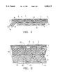
- FIG. 1 is a sectional view of the structure of an image input device in accordance with Embodiment 1 of the present invention
- FIG. 2 illustrates the principle of operation of an image input device in accordance with the present invention
- FIG. 3 is a sectional view of the structure of an image input device in accordance with Embodiment 2 of the present invention.
- FIG. 4 is a sectional view of the structure of an image input device in accordance with Embodiment 3 of the present invention.
- FIG. 5 is a sectional view of the structure of an image input device in accordance with Embodiment 4 of the present invention.
- FIG. 6 is a sectional view of the structure of a conventional image input device.
- the photoelectric conversion means may be two-dimensionally arranged.
- a reflection film may be disposed at an end of the light guide means.
- Both the light source and the light input means may be mounted to each end of the light guide means.
- a display means may be mounted on the photoelectric conversion means and the image input device may be integrated with the display means.
- the light emitted by the light source is made incident onto the light guide means at a predetermined angle by the light input means.
- the first and the second low refractive index layers are formed on vertically opposed surfaces of the light guide means.
- the light incident on the light guide means travels within the light guide means with repeating total reflection.
- the optical means are disposed so as to be partially in optical contact with the light guide means on the side of the first low refractive index layer, part of the traveling light is taken out toward the optical means.
- the taken-out light illuminates a document placed at the opposite side of the optical means.
- the reflected light from the document is collected onto the photoelectric conversion means by the lenses of the optical means. Since the reflected light from the document does not meet conditions for total reflection, the reflected light travels through the light guide means and then the second low refractive index layer to the photoelectric conversion means. Since a light path for illuminating the document is thus spacially separated from the photoelectric conversion means, arrangement and area of the photoelectric conversion means are not restricted by the light path of the illumination light.
- the light traveling in the light guide means is not allowed to leak out from the boundary with the second low refractive index layer by the nature of total reflection. Therefore, the photoelectric conversion means does not receive any other light than the reflected light from the document. Furthermore, since the reflected light from the document is collected by the lenses of the optical means and then incident onto the photoelectric conversion means, it is possible to prevent light mixing in adjacent pixels. Thus, high resolution can be realized.
- a two-dimensional image input device can be realized, which is thin, lightweight, and capable of reading at high speed with high resolution.
- the quantity of the illumination light can be increased and uneven distribution of the illumination light can be prevented.
- the quantity of the illumination light can be more increased and the uneven distribution of the illumination light can be more prevented.
- the document and an optical system for the illumination light such as the light guide means and the optical means are placed on the same side with respect to the photoelectric conversion means, and the opposite side is not used for mounting elements.
- the image input device and the image display device can be integrated without any optical influence to display.
- FIG. 1 is a sectional view of the structure of an image input device in accordance with Embodiment 1.
- This device is composed of a parallel transparent member 1 (the light guide means) for guiding illumination light, a low refractive index layer 2 (the second low refractive index layer) formed on the upper surface of the parallel transparent member 1, a low refractive index layer 3 (the first low refractive index layer) formed on the lower surface of the parallel transparent member 1, a photodiode 5 (the photoelectric conversion means) placed on the low refractive index layer 2, an electrode 6, a protection layer 7 to protect the photodiode 5 and the electrode 6, a lens array 4 (the optical means) mounted in contact with the parallel transparent member 1, a light source 10 to emit the illumination light, a lens 9 to collimate the illumination light emitted by the light source 10, and a prism 8 (the light input means) to direct the illumination light to the parallel transparent member 1.
- a parallel transparent member 1 the light guide means
- a low refractive index layer 2 the second
- the parallel transparent member 1 may be made of a glass plate, transparent plastic plate or transparent ceramic plate.
- the parallel transparent plate 1 functions as a light guide to guide the illumination light as well as functions as a substrate supporting the photodiode 5 and the like.
- the low refractive index layers 2 and 3 are composed of a medium having a lower refractive index than that of the parallel transparent member 1.
- the low refractive index layer 2 covers all over the upper surface of the parallel transparent member 1.
- the low refractive index layer 3 has extremely thin portions or completely removed portions.
- the lens array 4 is composed of a plastic material which has a refractive index close to that of the parallel transparent member 1.
- the lens array 4 is provided with a plurality of hemispherical convexes arranged on one surface. The other surface of the lens array 4 is flat. At the tops of the convexes, the lens array 4 is optically contacted with the parallel transparent member 1 via the extremely thin or completely removed portions of the low refractive index layer 3.
- a plurality of the photodiodes 5 are formed on the upper surface of the low refractive index layer 2, each photodiode defining one pixel. Light is incident on the photodiodes 5 from the side of the low refractive layer 2.
- the electrodes 6 are electrically connected with the photodiodes 5 and output signals from the photodiodes to outside. Where the photodiodes 5 are two-dimensionally arranged, another set of electrodes orthogonal to the electrodes 6 is provided.
- the photodiodes 5, the electrodes 6 and the protection layer 7 together define a sensor section.
- the light source 10 is composed of a halogen lamp, a white light source such as a fluorescent lamp or a light emitting diode.
- the prism 8 is used for making the light from the light source 10 incident on the parallel transparent member 1 at a predetermined angle.
- the prism may be substituted with a hologram.
- the low refractive index layers 2 and 3 may be formed by depositing a resin of low refractive index on the surfaces of the parallel transparent member 1 by a dip coating or a spin coating method.
- a resin of low refractive index on the surfaces of the parallel transparent member 1 by a dip coating or a spin coating method.
- an ion beam may be irradiated on a surface of the parallel transparent member to change the refractive index at the surface.
- the glass or plastic material may be dipped in a molten salt, and the nature of the material may be modified at the surface by ion exchange by applying an electric field in order to control the refractive index of the material.
- FIG. 2 like reference numbers denote like elements in FIG. 1.
- the light emitted by the light source 10 is converted to generally parallel light by the lens 9 and incident on an end surface of the prism 8.
- the light is not limited to parallel light, but it is preferable that the light is incident onto the parallel transparent member 1 at a constant incidence angle because the light is transmitted within the parallel transparent member 1 more effectively.
- the individual materials are selected so as to satisfy the following formula I:
- the incidence angle of a light beam onto the prism 8 must be set SQ as to allow for a considerable refraction at the boundary between the prism 8 and the parallel transparent member 1.
- FIG. 2 shows an enlarged view of FIG. 1.
- the parallel transparent member 1 and lens array 4 are optically contacted at the top portion 4a of each lens.
- the low refractive index layer 3 is extremely thin or completely removed at portions where the low refractive index layer 3 is in contact with the top portion 4a.
- a document 11 is placed on the flat lower surface of the lens array 4.
- the light beams 15 are transmitted in the parallel transparent member 1 with repeating total reflection.
- the lens array 4 has a refraction index near that of the parallel transparent member 1 and therefore does not satisfy the condition for the total reflection.
- the lens array 4 is optically contacted with the parallel transparent member 1. Accordingly the light beams are not totally reflected at the boundary and partially leak into the lens array 4. Light beams 12 leaking into the lens array 4 illuminate the document 11.
- Reflected light 13 from the document 11 is collected onto the photodiode 5 by the lens array 4.
- Light beams 14 passing through the lens array 4 never satisfy the total-reflection conditions. Therefore the light beams 14 pass through the parallel transparent member 1 and the low refraction index layer 2 and reach the photodiode 5.
- an photoelectric conversion output is generated according to contrast of the document 11, and an image of the document 11 is inputted.
- lens effect of the lens array 4 takes place at the boundary between the lens array 4 and the low refraction index layer 3
- the shape of the individual lenses of the lens array 4 must be designed in consideration of the refraction indexes of the lens array 4 and the low refraction index layer 3.
- a pitch of the photodiodes 5 do not necessarily agree with that of the lenses of the lens array 4, but the photodiodes and the lenses are preferably arranged so that light is collected in correspondence with the photodiodes 5.
- the area of the photodiodes may be changed according to where they are placed. More particularly, the area of the photodiodes is set smallest near the prism 8 and is gradually increased toward the opposite end. Alternatively, electric signals can be weighted for correction. However, to vary the area of the photodiodes is advantageous because the dynamic range of the photodiodes can effectively be used.
- the area of the photodiodes does not need reduction for the route of the illumination light. Since the area of the photodiodes is not restricted for the route of the illumination light and therefore can be set large, high-power signal output can be obtained. This contributes to improvement of resolution.
- the reflected light from the document is collected by the individual lenses of the lens array 4, it is possible to prevent light from entering from adjacent pixels. Thus a sharp signal output can be obtained.
- the route of the illumination light can be ensured regardless of the area and arrangement of the photodiodes. Therefore, in the case where the invention is adapted for a two-dimensional image sensor, there is spatial room obtained. Further, since a pixel can be protected against light from adjacent pixels, this embodiment can be developed into a two-dimensional image sensor without any problem.
- FIG. 3 shows a sectional view of the structure of an image input device in accordance with Embodiment 2.
- like reference numbers denote like elements in FIG. 1.
- This embodiment is structurally characterized in that a reflection film 20 is formed on an end surface 1a of a parallel transparent member 1 opposite to an end surface to which a prism 8 is mounted.
- the reflection film 20 is made of a metal film or an electrically conductive film and covers all over the end surface 1a of the parallel transparent member 1.
- FIG. 1 illustrating Embodiment 1 the light beams 15 traveling in the parallel transparent member 1 from the end to which the prism 8 is mounted escape out of the parallel transparent member 1 when the light beams reach the end surface 1a.
- the light beams 15 having reached the end surface 1a are reflected to be light beams 21 which reversely travels in the parallel transparent member 1.
- this embodiment can use light effectively and has the effect of increasing the amount of illumination light. Since the amount of illumination light can be increased especially in the neighborhood of the end surface 1a, this embodiment has the effect of improving a shading characteristic.
- this embodiment has the effect of improving a shading characteristic.
- FIG. 4 is a sectional view of the structure of an image input device in accordance with Embodiment 3.
- like reference numbers denote like elements in FIG. 1.
- This embodiment is characterized in that, to an end opposite to an end to which a prism 8 is mounted, another prism 30, lens 31 and light source 32 are mounted so that light is introduced from both ends of the parallel transparent member 1.
- the prism 30, lens 31 and light source 32 are equivalent to and have the same functions as the prism 8, lens 9 and light source 10, respectively.
- Embodiment 1 shown in FIG. 1 As discussed above, the shading problem is involved with Embodiment 1 shown in FIG. 1.
- the uniformity in distribution of the illumination light can greatly be improved.
- the quantity of light received by all the photodiodes 5 can be made substantially uniform without changing the area of the photodiodes 5.
- the quantity of illumination light is increased as a natural result.
- reflective films are additionally used at both the end surfaces of the parallel transparent member 1 as in the embodiment shown in FIG. 3, the above-described effects become more outstanding.
- FIG. 5 is a sectional view of the structure of an image input device in accordance with Embodiment 4.
- This device is composed of a parallel transparent member 1 to guide illumination light, a low refractive index layer 2 formed on an upper surface of the parallel transparent member 1, a low refractive index layer 3 formed on a lower surface of the parallel transparent member 1, photodiodes 5 placed above the low refractive index layer 3, TFTs 40 for driving liquid crystal arranged in alignment with the photodiodes 5, pixel electrodes 42 electrically connected with the TFTs 40, an insulating layer 43 covering the photodiodes 5 and the TFTs 40 to flatten the surface of the pixel electrodes 42, a liquid crystal layer 41 placed above the pixel electrodes 42, a glass substrate 44 to seal the liquid crystal layer 41 with opposed electrodes 44A formed on its surface, a lens array 4 disposed in contact with the parallel transparent member 1, a light source 10 to emit illumination light, a lens 9 to collimate the light
- the parallel transparent member 1, the TFTs 40 for driving liquid crystal, the pixel electrodes 42, the insulating layer 43, the liquid crystal layer 41 and the glass substrate 44 compose a reflection type liquid crystal panel as the display means.
- the display means is so designed that a displayed image is observed from the side of the glass substrate 44. Since the reflection type liquid crystal panel is usually a two-dimensional display device, the photodiodes are also two-dimensionally arranged for individual pixels.
- the TFT 40 for driving liquid crystal usable are an amorphous silicon TFT are a polysilicon TFT which are usually used as a switching element.
- the pixel electrode 42 is made of a metal film and also functions as a reflection plate for display light.
- the insulating layer 43 is formed of resin to keep insulation of the photodiodes 5 and the TFTs 40 and generally flatten the surface of the pixel electrodes 42.
- the liquid crystal layer 41 is formed of a guest-host liquid crystal so that it can be used as the reflection type panel.
- the glass substrate 44 usable are a transparent plastic plate and a transparent ceramic plate.
- the panel also includes a source electrode for display to control the TFTs 40, a gate electrode, and an external input electrode for externally outputting an inputted image signal, which are not shown.
- the electrode for display and the image input electrode can be shared.
- FIG. 2 The principle of operation of this embodiment as the image input device is shown in FIG. 2.
- Light traveling in the parallel transparent member 1 is taken out for illumination a document to the lens array 4 at contact points of the parallel transparent member 1 with the lens array 4.
- Light reflected from the document 11 is collected onto the photodiodes 5 by lens effect of the lens array 4.
- Amplifying circuits corresponding to the individual photodiodes 5 may be disposed near the photodiodes to allow the reflective type liquid crystal panel to display an image directly by image input signals read by the photodiodes 5.
- display can be made without amplifying circuits.
- This embodiment is characterized in that the image input device can be added to the reflection type liquid crystal panel without giving any influence to the reflection type liquid crystalpanel as a display device.
- the TFT 40 for driving liquid crystal is smaller than the pixel electrode 42, and accordingly there is sufficient room for forming a photodiode 5 beside the TFT 40.
- the TFTs 40 for driving the liquid crystal also receive light from the parallel transparent member 1 and this light might change characteristics of the TFTs for driving the liquid crystal.
- this problem can be avoided by forming a light-tight film on a bottom surface of the TFTs 40.
- Light-emission type display means other than the above-described reflection type liquid crystal panel which output and input display light only from one side include an LED array, electroluminescence (EL) panel, plasma display panel (PDP) and field emission display (FED).
- LED array electroluminescence
- PDP plasma display panel
- FED field emission display
- the optical path for illuminating the document can be made independent of the optical path of light reflected from the document, the area of the photoelectric conversion means is not reduced for the optical path of the illumination light. Therefore it is possible to obtain a large signal output and a high S/N ratio.
- the light traveling in the light guide means does not leak outside except where the light guide means is optically contacted with the lens. Accordingly, the illumination light is not incident onto the photoelectric conversion means directly, and a signal output of high contrast ratio can be obtained.
- the light reflected from the document is collected by each of the lenses and made incident onto the photoelectric conversion means. It is possible to prevent light from entering from adjacent pixels and therefore to improve the resolution of the input image.
- the present invention is applied for a so-called two-dimensional image sensor, it is possible to obtain more of the above-discussed effects. These effects are more outstanding with high-density, high-definition pixels.
- the quantity of the illumination light can be increased and uniformity in distribution of the illumination light can be improved.
- the quantity of the illumination light can further be increased and uniformity in distribution of the illumination light can further be improved.
- the constituents of the image input device including the optical system for the illumination light and the document setting can be all placed on the same side, viewed from the surface on which the photoelectric conversion means is placed.
- the image input device of the present invention can be integrated with a display in which light is outputted and inputted from only one side without any optical interference to each other.
Landscapes
- Physics & Mathematics (AREA)
- Engineering & Computer Science (AREA)
- Electromagnetism (AREA)
- General Physics & Mathematics (AREA)
- General Health & Medical Sciences (AREA)
- Artificial Intelligence (AREA)
- Computer Vision & Pattern Recognition (AREA)
- Health & Medical Sciences (AREA)
- Theoretical Computer Science (AREA)
- Toxicology (AREA)
- Facsimile Heads (AREA)
- Image Input (AREA)
- Transforming Light Signals Into Electric Signals (AREA)
- Light Receiving Elements (AREA)
- Liquid Crystal (AREA)
- Solid State Image Pick-Up Elements (AREA)
- Facsimile Scanning Arrangements (AREA)
Applications Claiming Priority (2)
| Application Number | Priority Date | Filing Date | Title |
|---|---|---|---|
| JP8-347042 | 1996-12-26 | ||
| JP34704296A JP3180043B2 (ja) | 1996-12-26 | 1996-12-26 | 画像入力装置 |
Publications (1)
| Publication Number | Publication Date |
|---|---|
| US6002139A true US6002139A (en) | 1999-12-14 |
Family
ID=18387535
Family Applications (1)
| Application Number | Title | Priority Date | Filing Date |
|---|---|---|---|
| US08/977,833 Expired - Fee Related US6002139A (en) | 1996-12-26 | 1997-11-26 | Image input device having a refractive index light guide and lenses |
Country Status (2)
| Country | Link |
|---|---|
| US (1) | US6002139A (ja) |
| JP (1) | JP3180043B2 (ja) |
Cited By (12)
| Publication number | Priority date | Publication date | Assignee | Title |
|---|---|---|---|---|
| US6104021A (en) * | 1997-04-09 | 2000-08-15 | Nec Corporation | Solid state image sensing element improved in sensitivity and production cost, process of fabrication thereof and solid state image sensing device using the same |
| US6266032B1 (en) * | 1997-10-31 | 2001-07-24 | Alps Electric Co., Ltd. | Coordinate-inputting device and method for making same |
| FR2822269A1 (fr) * | 2001-03-15 | 2002-09-20 | Teb | Systeme de marquage et d'identification optique |
| US20030102875A1 (en) * | 2001-11-22 | 2003-06-05 | Toshimitsu Fujiwara | Input device |
| US20030160247A1 (en) * | 2001-12-27 | 2003-08-28 | Seiko Epson Corporation | Apparatus and method for manufacturing electro-optical devices |
| US20050141837A1 (en) * | 2003-12-30 | 2005-06-30 | Au Optronics Corporation | Bendable light guide |
| EP1578617A1 (fr) * | 2003-01-03 | 2005-09-28 | Banque De France | Dispositif de securite en guide d'onde |
| US20080088731A1 (en) * | 2005-01-20 | 2008-04-17 | Yasuhiro Tanaka | Lens Array and Image Sensor Including Lens Array |
| US20090091910A1 (en) * | 2007-10-05 | 2009-04-09 | Hsin-Chin Lee | Keypad with increased refractive index |
| CN101752441B (zh) * | 2008-12-15 | 2012-05-23 | 富士迈半导体精密工业(上海)有限公司 | 便携式供电装置 |
| US20160097890A1 (en) * | 2009-04-21 | 2016-04-07 | Sergiy Vasylyev | Collimating illumination systems employing planar waveguide |
| US11175530B2 (en) * | 2017-10-20 | 2021-11-16 | Samsung Display Co., Ltd. | Liquid crystal display panel and liquid crystal display device including the same |
Families Citing this family (2)
| Publication number | Priority date | Publication date | Assignee | Title |
|---|---|---|---|---|
| JP4759511B2 (ja) * | 2004-04-19 | 2011-08-31 | 株式会社日立製作所 | 撮像機能一体型表示装置 |
| US7426259B2 (en) * | 2004-08-31 | 2008-09-16 | Xerox Corporation | Imaging system and method that removes an electrical charge from a sensor |
Citations (5)
| Publication number | Priority date | Publication date | Assignee | Title |
|---|---|---|---|---|
| JPS63214058A (ja) * | 1987-03-02 | 1988-09-06 | Hitachi Ltd | 密着イメ−ジセンサ |
| JPH05347396A (ja) * | 1991-03-25 | 1993-12-27 | Semiconductor Energy Lab Co Ltd | 画像読み取り装置 |
| US5416608A (en) * | 1991-07-04 | 1995-05-16 | Minolta Camera Kabushiki Kaisha | Image reading apparatus |
| US5430462A (en) * | 1992-12-07 | 1995-07-04 | Sharp Kabushiki Kaisha | Image input device-integrated type display device |
| JPH08191371A (ja) * | 1994-11-09 | 1996-07-23 | Fuji Xerox Co Ltd | イメージセンサ |
-
1996
- 1996-12-26 JP JP34704296A patent/JP3180043B2/ja not_active Expired - Fee Related
-
1997
- 1997-11-26 US US08/977,833 patent/US6002139A/en not_active Expired - Fee Related
Patent Citations (5)
| Publication number | Priority date | Publication date | Assignee | Title |
|---|---|---|---|---|
| JPS63214058A (ja) * | 1987-03-02 | 1988-09-06 | Hitachi Ltd | 密着イメ−ジセンサ |
| JPH05347396A (ja) * | 1991-03-25 | 1993-12-27 | Semiconductor Energy Lab Co Ltd | 画像読み取り装置 |
| US5416608A (en) * | 1991-07-04 | 1995-05-16 | Minolta Camera Kabushiki Kaisha | Image reading apparatus |
| US5430462A (en) * | 1992-12-07 | 1995-07-04 | Sharp Kabushiki Kaisha | Image input device-integrated type display device |
| JPH08191371A (ja) * | 1994-11-09 | 1996-07-23 | Fuji Xerox Co Ltd | イメージセンサ |
Cited By (22)
| Publication number | Priority date | Publication date | Assignee | Title |
|---|---|---|---|---|
| US6291811B1 (en) | 1997-04-09 | 2001-09-18 | Nec Corporation | Solid state image sensing element improved in sensitivity and production cost, process of fabrication thereof and solid state image sensing device using the same |
| US6104021A (en) * | 1997-04-09 | 2000-08-15 | Nec Corporation | Solid state image sensing element improved in sensitivity and production cost, process of fabrication thereof and solid state image sensing device using the same |
| US6266032B1 (en) * | 1997-10-31 | 2001-07-24 | Alps Electric Co., Ltd. | Coordinate-inputting device and method for making same |
| US20040144845A1 (en) * | 2001-03-15 | 2004-07-29 | Louis Bidault | Optical identification and marking system |
| FR2822269A1 (fr) * | 2001-03-15 | 2002-09-20 | Teb | Systeme de marquage et d'identification optique |
| WO2002075638A1 (fr) * | 2001-03-15 | 2002-09-26 | Teb | Systeme de marquage et d'identification optique |
| US7191946B2 (en) | 2001-03-15 | 2007-03-20 | Teb | Optical identification and marking system |
| US7019765B2 (en) * | 2001-11-22 | 2006-03-28 | Omron Corporation | Input device |
| US20030102875A1 (en) * | 2001-11-22 | 2003-06-05 | Toshimitsu Fujiwara | Input device |
| US7714328B2 (en) * | 2001-12-27 | 2010-05-11 | Seiko Epson Corporation | Apparatus and method for manufacturing electro-optical devices |
| US20030160247A1 (en) * | 2001-12-27 | 2003-08-28 | Seiko Epson Corporation | Apparatus and method for manufacturing electro-optical devices |
| US7211838B2 (en) * | 2001-12-27 | 2007-05-01 | Seiko Epson Corporation | Apparatus and method for manufacturing electro-optical devices |
| US20070170429A1 (en) * | 2001-12-27 | 2007-07-26 | Seiko Epson Corporation | Apparatus and method for manufacturing electro-optical devices |
| EP1578617A1 (fr) * | 2003-01-03 | 2005-09-28 | Banque De France | Dispositif de securite en guide d'onde |
| US20050141837A1 (en) * | 2003-12-30 | 2005-06-30 | Au Optronics Corporation | Bendable light guide |
| US20080088731A1 (en) * | 2005-01-20 | 2008-04-17 | Yasuhiro Tanaka | Lens Array and Image Sensor Including Lens Array |
| CN100520822C (zh) * | 2005-01-20 | 2009-07-29 | 松下电器产业株式会社 | 透镜阵列和包括透镜阵列的图像传感器 |
| US20090091910A1 (en) * | 2007-10-05 | 2009-04-09 | Hsin-Chin Lee | Keypad with increased refractive index |
| CN101752441B (zh) * | 2008-12-15 | 2012-05-23 | 富士迈半导体精密工业(上海)有限公司 | 便携式供电装置 |
| US20160097890A1 (en) * | 2009-04-21 | 2016-04-07 | Sergiy Vasylyev | Collimating illumination systems employing planar waveguide |
| US9880342B2 (en) * | 2009-04-21 | 2018-01-30 | Svv Technology Innovations, Inc. | Collimating illumination systems employing planar waveguide |
| US11175530B2 (en) * | 2017-10-20 | 2021-11-16 | Samsung Display Co., Ltd. | Liquid crystal display panel and liquid crystal display device including the same |
Also Published As
| Publication number | Publication date |
|---|---|
| JP3180043B2 (ja) | 2001-06-25 |
| JPH10190944A (ja) | 1998-07-21 |
Similar Documents
| Publication | Publication Date | Title |
|---|---|---|
| US6002139A (en) | Image input device having a refractive index light guide and lenses | |
| US5086218A (en) | Photo sensor and its manufacturing method and an image reading apparatus having this photo sensor | |
| US4908718A (en) | Image reading apparatus having a light shielding layer arranged on the sides of the substrate and protective layers of a photo sensor | |
| US6858983B2 (en) | Display device having conical transparent members covering electroluminescent elements | |
| US4446364A (en) | Photoelectric converter on a transmissive substrate having light shielding | |
| JP3008859B2 (ja) | 薄型光源を用いたイメージセンサ装置 | |
| US7497609B2 (en) | Illuminating device and liquid crystal display apparatus | |
| KR970006788B1 (ko) | 밀착형 이미지 센서 | |
| CN113504647B (zh) | 一种可穿戴显示装置及其驱动方法 | |
| US5164580A (en) | Electroluminescent light-source-incorporated image sensor | |
| WO2019077917A1 (ja) | 光ラインセンサユニット | |
| EP0707407B1 (en) | An image display/input apparatus | |
| JPH0415630B2 (ja) | ||
| CN113433734B (zh) | 显示装置 | |
| JP3067460B2 (ja) | 画像入出力装置 | |
| JPH11234474A (ja) | 密着型イメージセンサ | |
| JPS5962267A (ja) | 密着型読み取り装置 | |
| JP3307978B2 (ja) | イメージセンサ | |
| JP2769812B2 (ja) | 原稿読み取り装置 | |
| JP3687104B2 (ja) | 光学装置 | |
| JPH02220557A (ja) | 画像読み取り装置 | |
| JPS6355221B2 (ja) | ||
| JPS5941629B2 (ja) | 文字図形読取装置 | |
| KR950009643B1 (ko) | 화상판독장치 | |
| JPH02257758A (ja) | 画像読み取り装置 |
Legal Events
| Date | Code | Title | Description |
|---|---|---|---|
| AS | Assignment |
Owner name: SHARP KABUSHIKI KAISHA, JAPAN Free format text: ASSIGNMENT OF ASSIGNORS INTEREST;ASSIGNOR:KATAGIRI, MASAYUKI;REEL/FRAME:008895/0512 Effective date: 19971107 |
|
| FPAY | Fee payment |
Year of fee payment: 4 |
|
| FPAY | Fee payment |
Year of fee payment: 8 |
|
| REMI | Maintenance fee reminder mailed | ||
| LAPS | Lapse for failure to pay maintenance fees | ||
| STCH | Information on status: patent discontinuation |
Free format text: PATENT EXPIRED DUE TO NONPAYMENT OF MAINTENANCE FEES UNDER 37 CFR 1.362 |
|
| FP | Lapsed due to failure to pay maintenance fee |
Effective date: 20111214 |