US5726489A - Film carrier semiconductor device - Google Patents
Film carrier semiconductor device Download PDFInfo
- Publication number
- US5726489A US5726489A US08/531,271 US53127195A US5726489A US 5726489 A US5726489 A US 5726489A US 53127195 A US53127195 A US 53127195A US 5726489 A US5726489 A US 5726489A
- Authority
- US
- United States
- Prior art keywords
- chip
- film
- semiconductor device
- carrier
- electrodes
- Prior art date
- Legal status (The legal status is an assumption and is not a legal conclusion. Google has not performed a legal analysis and makes no representation as to the accuracy of the status listed.)
- Expired - Fee Related
Links
Images



Classifications
-
- H—ELECTRICITY
- H10—SEMICONDUCTOR DEVICES; ELECTRIC SOLID-STATE DEVICES NOT OTHERWISE PROVIDED FOR
- H10W—GENERIC PACKAGES, INTERCONNECTIONS, CONNECTORS OR OTHER CONSTRUCTIONAL DETAILS OF DEVICES COVERED BY CLASS H10
- H10W72/00—Interconnections or connectors in packages
- H10W72/071—Connecting or disconnecting
-
- H—ELECTRICITY
- H10—SEMICONDUCTOR DEVICES; ELECTRIC SOLID-STATE DEVICES NOT OTHERWISE PROVIDED FOR
- H10W—GENERIC PACKAGES, INTERCONNECTIONS, CONNECTORS OR OTHER CONSTRUCTIONAL DETAILS OF DEVICES COVERED BY CLASS H10
- H10W74/00—Encapsulations, e.g. protective coatings
- H10W74/10—Encapsulations, e.g. protective coatings characterised by their shape or disposition
- H10W74/111—Encapsulations, e.g. protective coatings characterised by their shape or disposition the semiconductor body being completely enclosed
- H10W74/129—Encapsulations, e.g. protective coatings characterised by their shape or disposition the semiconductor body being completely enclosed forming a chip-scale package [CSP]
-
- H—ELECTRICITY
- H10—SEMICONDUCTOR DEVICES; ELECTRIC SOLID-STATE DEVICES NOT OTHERWISE PROVIDED FOR
- H10W—GENERIC PACKAGES, INTERCONNECTIONS, CONNECTORS OR OTHER CONSTRUCTIONAL DETAILS OF DEVICES COVERED BY CLASS H10
- H10W42/00—Arrangements for protection of devices
- H10W42/20—Arrangements for protection of devices protecting against electromagnetic or particle radiation, e.g. light, X-rays, gamma-rays or electrons
-
- H—ELECTRICITY
- H10—SEMICONDUCTOR DEVICES; ELECTRIC SOLID-STATE DEVICES NOT OTHERWISE PROVIDED FOR
- H10W—GENERIC PACKAGES, INTERCONNECTIONS, CONNECTORS OR OTHER CONSTRUCTIONAL DETAILS OF DEVICES COVERED BY CLASS H10
- H10W70/00—Package substrates; Interposers; Redistribution layers [RDL]
- H10W70/40—Leadframes
- H10W70/453—Leadframes comprising flexible metallic tapes
-
- H—ELECTRICITY
- H10—SEMICONDUCTOR DEVICES; ELECTRIC SOLID-STATE DEVICES NOT OTHERWISE PROVIDED FOR
- H10W—GENERIC PACKAGES, INTERCONNECTIONS, CONNECTORS OR OTHER CONSTRUCTIONAL DETAILS OF DEVICES COVERED BY CLASS H10
- H10W70/00—Package substrates; Interposers; Redistribution layers [RDL]
- H10W70/60—Insulating or insulated package substrates; Interposers; Redistribution layers
- H10W70/62—Insulating or insulated package substrates; Interposers; Redistribution layers characterised by their interconnections
- H10W70/65—Shapes or dispositions of interconnections
-
- H—ELECTRICITY
- H10—SEMICONDUCTOR DEVICES; ELECTRIC SOLID-STATE DEVICES NOT OTHERWISE PROVIDED FOR
- H10W—GENERIC PACKAGES, INTERCONNECTIONS, CONNECTORS OR OTHER CONSTRUCTIONAL DETAILS OF DEVICES COVERED BY CLASS H10
- H10W70/00—Package substrates; Interposers; Redistribution layers [RDL]
- H10W70/60—Insulating or insulated package substrates; Interposers; Redistribution layers
- H10W70/67—Insulating or insulated package substrates; Interposers; Redistribution layers characterised by their insulating layers or insulating parts
- H10W70/68—Shapes or dispositions thereof
- H10W70/685—Shapes or dispositions thereof comprising multiple insulating layers
-
- H—ELECTRICITY
- H10—SEMICONDUCTOR DEVICES; ELECTRIC SOLID-STATE DEVICES NOT OTHERWISE PROVIDED FOR
- H10W—GENERIC PACKAGES, INTERCONNECTIONS, CONNECTORS OR OTHER CONSTRUCTIONAL DETAILS OF DEVICES COVERED BY CLASS H10
- H10W90/00—Package configurations
- H10W90/701—Package configurations characterised by the relative positions of pads or connectors relative to package parts
-
- H—ELECTRICITY
- H10—SEMICONDUCTOR DEVICES; ELECTRIC SOLID-STATE DEVICES NOT OTHERWISE PROVIDED FOR
- H10W—GENERIC PACKAGES, INTERCONNECTIONS, CONNECTORS OR OTHER CONSTRUCTIONAL DETAILS OF DEVICES COVERED BY CLASS H10
- H10W72/00—Interconnections or connectors in packages
- H10W72/071—Connecting or disconnecting
- H10W72/072—Connecting or disconnecting of bump connectors
- H10W72/07251—Connecting or disconnecting of bump connectors characterised by changes in properties of the bump connectors during connecting
-
- H—ELECTRICITY
- H10—SEMICONDUCTOR DEVICES; ELECTRIC SOLID-STATE DEVICES NOT OTHERWISE PROVIDED FOR
- H10W—GENERIC PACKAGES, INTERCONNECTIONS, CONNECTORS OR OTHER CONSTRUCTIONAL DETAILS OF DEVICES COVERED BY CLASS H10
- H10W72/00—Interconnections or connectors in packages
- H10W72/20—Bump connectors, e.g. solder bumps or copper pillars; Dummy bumps; Thermal bumps
Definitions
- the present invention relates to a film carrier semiconductor device and, more particularly, to a film carrier semiconductor device which can advantageously be mounted on, for example, a circuit board at a high density.
- the semiconductor device comprises a package and a semiconductor chip (hereinafter, also referred to as a chip) contained in the package.
- a semiconductor device having a high pin count can be obtained by inner lead bonding or by area array bonding.
- the inner lead bonding and the area array bonding are expected to be inevitable for the field of the semiconductors.
- the inner lead bonding is used to make electrical contact between the chip and the leads within the package.
- Various bonding technologies are available to achieve this inner lead bonding.
- Wire bonding is the most extensively used electrical interconnection process. In this process, fine wires are used to make electrical contact between the bonding pads on the chip and the corresponding leads on the package.
- the wire diameter is typically from 20 to 30 micrometers.
- Wire bonding techniques include thermocompression bonding, ultrasonic bonding, and thermosonic bonding.
- the use of the fine wires limits the number of interconnections available in one package.
- the recent demands for the semiconductor devices with a high pin count thus causes a problem of poor connections between the wire and the bonding pads.
- the wire bonding has been replaced with wireless bonding.
- the wireless bonding is also called gang bonding, with which all bumps on the electrode pads (hereinafter, also referred to as pads) are bonded simultaneously to the leads.
- Wireless bonding techniques include tape automated bonding (TAB) and flip-chip bonding.
- TAB bonding is also referred to as tape carrier bonding.
- the TAB technique a laminated tape of gold-plated copper foil etched in the form of leads is bonded to the bumps on the chip pads.
- the elimination of the wire bonding is advantageous from viewpoints of size reduction and highly integrated packaging of the device.
- the flip-chip bonding requires to make a raised metallic bump of solder on the chip. The chip is then inverted and bonded face down to the substrate interconnection pattern. This process lends itself to production of semiconductor devices with a high pin count and a smaller pitch.
- this technique is also advantageous to provide a fast, low-noise semiconductor device with the short length of the interconnections.
- the TAB and flip-chip bonding techniques use the bumps provided between the chip and the film (package) to make electrical interconnection between them. These techniques are disclosed in, for example, Japanese Patent Laid-open Nos. 5-129366 and 6-77293.
- the film carrier semiconductor device disclosed in these laid-open publications uses the bumps for the electrical interconnection between the chip and the carrier film.
- the semiconductor chip and the carrier film are electrically connected during the assembly process.
- the bumps are used only for the purpose of connecting the film carrier semiconductor device with, for example, a circuit board.
- the film carrier semiconductor device of the type described comprises a semiconductor chip and a carrier film. Contact pads are provided on the semiconductor chip at one side thereof. The contact pads are arranged along the periphery of the semiconductor chip. Interconnecting layers are provided on the carrier film.
- the carrier film is also provided with through-holes and openings formed therein. The openings are formed at the position corresponding to the contact pads.
- the bumps are formed on corresponding outer contact pads arranged as an array on the carrier film on the side facing to the substrate.
- the bumps are formed both within and outside the area corresponding to a chip mounting region. In this event, the bumps may be formed along the periphery of the chip and are connected to the chip electrodes through the interconnection layers.
- This structure causes a noise problem of the film carrier semiconductor device. More specifically, the bumps are arranged into an array and thus the bump located at or around the center of the array is connected to the corresponding chip electrode through a long interconnection layer. With a higher pin count, a longer interconnection layer may be required for the interconnection between the bump and the chip electrode. This raises the necessity to reduce the width of the wiring for a smaller semiconductor package. Such a long and thin wiring tends to be affected by noise from outside.
- a semiconductor IC comprises a conductive region for power supply provided on a package on which a semiconductor chip is mounted.
- the conductive region surrounds the semiconductor chip and is connected with power supply pads on the semiconductor chip.
- the technique disclosed in this laid-open publication is provided only for the purpose of reducing the number of outer pins for the power supply.
- the power supply pads on the semiconductor chip are connected with the conductive region through bonding wires.
- the semiconductor IC disclosed there is associated with the wire bonding process, which is outside the scope of the field to which the present invention relates.
- an object of the present invention is to provide a film carrier semiconductor device which is less affected by noise, has good electrical properties, and can be meet a requirement, if any, for having a higher pin count.
- a film carrier semiconductor device comprising a semiconductor bare chip having chip electrodes on one surface thereof; a resin sealing the semiconductor bare chip; and a carrier film including a mounting region on a top surface, the semiconductor bare chip being adhered to said carrier film in said mounting region, the carrier film being provided with interconnections on said top surface connected to said chip electrodes, the film carrier semiconductor device further comprising a noise blocking layer provided on said top surface along the periphery thereof outside the chip mounting region so as to surround the interconnections, said resin sealing said noise blocking layer.
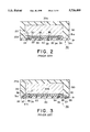
- FIG. 1 is a plan view of a conventional film carrier semiconductor device
- FIG. 2 is a cross-sectional view taken on line A-A' of FIG. 1;
- FIG. 3 is a cross-sectional view taken on line B-B' of FIG. 1;
- FIG. 4 is a plan view of a film carrier semiconductor device according to an embodiment of the present invention.
- FIG. 5 is a cross-sectional view taken on line A-A' of FIG. 4;
- FIG. 6 is a cross-sectional view taken on line B-B' of FIG. 4.
- a film carrier semiconductor device 10' comprises a semiconductor bare chip 20 and a carrier film 30.
- An adhesion film 40 is interposed between the bare chip 20 and the carrier film 30.
- the adhesion film 40 is smaller than the semiconductor bare chip 20 and has a thickness of about several ten micrometers.
- the semiconductor bare chip 20 is prepared by using, for example, a well-known wafer manufacturing technique and has a first surface 20a and a second surface 20b.
- a plurality of contact pads (chip electrodes) 21 are provided on the bare chip 20 on the side of the second surface 20b.
- the contact pads 21 are arranged along the periphery of the bare chip 20 and each serves as an electrode for signals, for the power supply, or for the ground.
- the contact pads 21 may be, however, provided on the bare chip 20 within an active region.
- the contact pads 21 are typically made of an aluminum-based alloy.
- the bare chip 20 is also provided with a passivation film 22 formed on the second surface 20b thereof.
- the passivation film 22 may be made of, for example, polyimide, silicon nitride, or silicon oxide.
- the carrier film 30 comprises an organic insulation film 31.
- the organic insulation film 31 may be, for example, a polyimide-based insulation film.
- the organic insulation film 31 has a first surface 31a and a second surface 31b.
- Interconnection layers 32 are provided on the organic insulation film 31 on the side of the first surface 31a.
- Through-holes 33 are formed in the insulation film 31. One end of each through-hole 33 faces the interconnection layer 32.
- Each through-hole 33 passes through the insulation film 31 to the second surface 31b thereof.
- the insulation film 31 is also provided with openings 34 penetrating through the film.
- the openings 34 are formed at the position corresponding to the contact pads 21.
- Each through-hole 33 is filled with a conductive electrode 35.
- each opening 34 is filled with a filler material 36.
- the conductive electrode 35 contacts with one end of the interconnection layer 32.
- the other end of the interconnection layer 32 reaches between the contact pad 21 and the opening 34.
- solder bumps (bump electrodes) 37 are formed on corresponding outer contact pads arranged as an array on the carrier film 30 at the second surface 31b thereof.
- the solder bumps 37 may be formed by using a method disclosed in, for example, Japanese Patent Laid-open No. 49-52973.
- the solder bumps 37 are formed by soldering a solder wire by using the wire bonding process on the surfaces of the semiconductor device corresponding to the pads on the chip. The balls are then bonded to the pads, following which the wires are cut. Some of the solder bumps 37 are formed within the area corresponding to a bare chip mounting region where the bare chip 20 is mounted. These solder bumps 37 are defined herein as a first group of the solder bumps.
- the remaining solder bumps 37 are formed outside the area corresponding to the bare chip mounting region. These bumps are defined herein as a second group of the solder bumps. If the bare chip mounting region is not enough for the bump electrodes, the bump electrodes 37 may be formed along the periphery of the chip as shown in FIG. 3. Considering the easy mounting of the semiconductor device on the circuit board or the like, the bump electrodes 37 may be arranged into an array at a pitch of 0.5 mm. As an example, the semiconductor chip mounting region has an area of 7 mm square available for forming the bump electrodes. Only two hundred and twenty-five pins, at maximum, can be formed within this region. To provide a region larger than the chip size for the bump formation, molding may advantageously be used. FIG.
- the bump electrodes are arranged even along the periphery of the chip and are connected to the chip electrodes through the interconnection layer.
- This structure causes a noise problem of the film carrier semiconductor device 10'.
- the bump electrodes for mounting are arranged into an array. Accordingly, the bump electrode at or around the center of the array is connected to the corresponding chip electrode through a long interconnection layer. A longer interconnection layer may be required for the interconnection between the bump electrode and the chip electrode of the semiconductor device having a higher pin count. It is thus necessary to reduce the width of the wiring for a smaller semiconductor package. Such a long and thin wiring tends to be affected by noise from outside.
- FIG. 4 is a plan view of a film carrier semiconductor device according to an embodiment of the present invention.
- FIG. 5 is a cross-sectional view taken on line A-A' of FIG. 4 while FIG. 6 is a cross-sectional view taken on line B-B' of FIG. 4.
- a noise blocking layer is a difference between a film carrier semiconductor device 10 and the film carrier semiconductor device 10'.
- the film carrier semiconductor device 10 according to an embodiment of the present invention comprises the noise blocking layer 60 provided on the carrier film 30 along the periphery thereof on the side of the first surface 31a.
- the noise blocking layer 60 is outside the bare chip mounting region to form a closed loop.
- the noise blocking layer surrounds the interconnection layers 32 as shown in FIGS. 4 through 6.
- the chip electrodes 21 are located inside the closed loop of the noise blocking layer 60.
- the noise blocking layer 60 is electrically connected to at least one chip electrode 21a. In this embodiment, twenty chip electrodes 21a are connected to the noise blocking layer 60. The remaining chip electrodes, which are depicted by 21b, are connected to the bump electrodes 37. It is noted that there is no limitation on the number of the chip electrodes 21 and 21b.
- the noise blocking layer 60 is either a power supply layer or a ground layer. More specifically, the noise blocking layer 60 serves as the power supply layer when it is electrically connected to the chip electrode(s) 21a used as the electrode(s) for the power supply. Likewise, the noise blocking layer 60 acts as the ground layer when it is connected to the chip electrode(s) 21a used as the electrode(s) for the ground.
- the bump electrodes 37 located within the noise blocking loop are all for transmitting signals (bump electrodes 37a).
- the bump electrode 37b which is located outside the chip mounting region and is connected to the chip electrode 21b is used for the transmission of signals. In this event, the bump electrode 37b is not in contact with the noise blocking layer 60 as clearly shown in FIG. 6. It should be noted that the bump electrode 37b is not necessarily formed outside the chip mounting region. These bump electrodes 37b may be provided within the chip mounting region if this region has enough area for the bump electrodes 37a and 37b. The remaining bump electrodes 37c are either for grounding or for the power supply.
- the bump electrodes 37c are used for grounding when the noise blocking layer 60 is the ground layer.
- the bump electrodes 37c serve as the electrodes for the power supply when the noise blocking layer 60 is the power supply layer.
- the noise blocking layer 60 is made of a conductive material and is formed to have as large a width as possible in order to reduce the inductance thereof. In this event, the "width" of the noise blocking layer 60 means the distance in the direction depicted by W in FIG. 4.
- the demand for a larger number of bump electrodes 37 makes it necessary to use a longer interconnection layer 32. It is thus required to reduce the width of the interconnection layer in order to reduce the size of the semiconductor device.
- Such film carrier semiconductor device as illustrated in FIG. 1 is more likely to be affected by signal noise.
- the noise blocking layer 60 serves to reduce or even eliminate noise on the interconnection layers 32 after being connected with the chip electrodes.
- the noise blocking layer may be formed of two layers, i.e., the ground layer and the power supply layer rather than being formed as a single layer. In such a case, an insulation film or layer is interposed between the power supply layer and the ground layer.
Landscapes
- Wire Bonding (AREA)
- Structures Or Materials For Encapsulating Or Coating Semiconductor Devices Or Solid State Devices (AREA)
Applications Claiming Priority (2)
| Application Number | Priority Date | Filing Date | Title |
|---|---|---|---|
| JP6-237854 | 1994-09-30 | ||
| JP6237854A JP2546192B2 (ja) | 1994-09-30 | 1994-09-30 | フィルムキャリア半導体装置 |
Publications (1)
| Publication Number | Publication Date |
|---|---|
| US5726489A true US5726489A (en) | 1998-03-10 |
Family
ID=17021403
Family Applications (1)
| Application Number | Title | Priority Date | Filing Date |
|---|---|---|---|
| US08/531,271 Expired - Fee Related US5726489A (en) | 1994-09-30 | 1995-09-20 | Film carrier semiconductor device |
Country Status (4)
| Country | Link |
|---|---|
| US (1) | US5726489A (de) |
| EP (1) | EP0704900A3 (de) |
| JP (1) | JP2546192B2 (de) |
| KR (1) | KR100209993B1 (de) |
Cited By (44)
| Publication number | Priority date | Publication date | Assignee | Title |
|---|---|---|---|---|
| US5866949A (en) * | 1996-12-02 | 1999-02-02 | Minnesota Mining And Manufacturing Company | Chip scale ball grid array for integrated circuit packaging |
| US5892288A (en) * | 1997-05-30 | 1999-04-06 | Mitsubishi Denki Kabushiki Kaisha | Semiconductor integrated circuit device |
| US5990563A (en) * | 1995-12-29 | 1999-11-23 | Lg Semicon Co., Ltd. | Semiconductor package having a connection member |
| WO2000008684A1 (en) * | 1998-08-05 | 2000-02-17 | Fairchild Semiconductor Corporation | High performance flip chip package |
| US6048753A (en) * | 1996-04-02 | 2000-04-11 | Micron Technology, Inc. | Standardized bonding location process and apparatus |
| US6097082A (en) * | 1997-11-21 | 2000-08-01 | Nec Corporation | Semiconductor device |
| US6194778B1 (en) * | 1996-08-16 | 2001-02-27 | Sony Corporation | Semiconductor package with improved cross talk and grounding, and method of manufacturing same |
| US6265770B1 (en) * | 1998-03-24 | 2001-07-24 | Seiko Epson Corporation | Mounting structure of semiconductor chip, liquid crystal device, and electronic equipment |
| US6265759B1 (en) * | 1995-09-08 | 2001-07-24 | Tessera, Inc. | Laterally situated stress/strain relieving lead for a semiconductor chip package |
| US6281450B1 (en) * | 1997-06-26 | 2001-08-28 | Hitachi Chemical Company, Ltd. | Substrate for mounting semiconductor chips |
| US6331737B1 (en) * | 1998-08-25 | 2001-12-18 | Texas Instruments Incorporated | Method of encapsulating thin semiconductor chip-scale packages |
| WO2001086718A3 (en) * | 2000-05-11 | 2002-04-04 | Koninkl Philips Electronics Nv | Semiconductor device with fuses and method of manufacturing same |
| US6396159B1 (en) * | 1997-06-27 | 2002-05-28 | Nec Corporation | Semiconductor device |
| US6486052B1 (en) * | 1999-08-16 | 2002-11-26 | Nec Corporation | Package having terminated plating layer and its manufacturing method |
| US20030001247A1 (en) * | 2001-06-18 | 2003-01-02 | International Rectifier Corporation | High voltage semiconductor device housing with increased clearance between housing can and die for improved flux flushing |
| US6544816B1 (en) * | 1999-08-20 | 2003-04-08 | Texas Instruments Incorporated | Method of encapsulating thin semiconductor chip-scale packages |
| US20030132531A1 (en) * | 2001-03-28 | 2003-07-17 | Martin Standing | Surface mounted package with die bottom spaced from support board |
| US6611063B1 (en) * | 1999-09-16 | 2003-08-26 | Nec Electronics Corporation | Resin-encapsulated semiconductor device |
| US6657562B2 (en) * | 2001-02-14 | 2003-12-02 | Siemens Aktiengesellschaft | Data compression/decompression method and apparatus |
| US6674174B2 (en) * | 2001-11-13 | 2004-01-06 | Skyworks Solutions, Inc. | Controlled impedance transmission lines in a redistribution layer |
| US20040032013A1 (en) * | 2002-08-15 | 2004-02-19 | Cobbley Chad A. | Semiconductor dice packages employing at least one redistribution layer and methods of fabrication |
| US20040099950A1 (en) * | 2002-11-18 | 2004-05-27 | Takashi Ohsumi | Semiconductor device |
| US20040099940A1 (en) * | 2002-11-22 | 2004-05-27 | International Rectifier Corporation | Semiconductor device having clips for connecting to external elements |
| US20040104489A1 (en) * | 2001-03-28 | 2004-06-03 | International Rectifier Corporation | Direct fet device for high frequency application |
| US20040224438A1 (en) * | 2000-04-04 | 2004-11-11 | International Rectifier Corporation | Chip scale surface mounted device and process of manufacture |
| US20050098902A1 (en) * | 2003-11-11 | 2005-05-12 | Sheng-Hsiung Ho | Anisotropic conductive film bonding pad |
| US20050133937A1 (en) * | 2003-12-17 | 2005-06-23 | Haruki Ito | Semiconductor device, method of manufacturing thereof, circuit board and electronic apparatus |
| US6967412B2 (en) | 2001-08-24 | 2005-11-22 | International Rectifier Corporation | Wafer level underfill and interconnect process |
| US20050269677A1 (en) * | 2004-05-28 | 2005-12-08 | Martin Standing | Preparation of front contact for surface mounting |
| US20060043569A1 (en) * | 2004-08-27 | 2006-03-02 | Benson Peter A | Low temperature methods of forming back side redistribution layers in association with through wafer interconnects, semiconductor devices including same, and assemblies |
| US20060240598A1 (en) * | 2005-04-20 | 2006-10-26 | International Rectifier Corporation | Chip scale package |
| US20060249836A1 (en) * | 2005-04-22 | 2006-11-09 | Andy Farlow | Chip-scale package |
| US20070012947A1 (en) * | 2002-07-15 | 2007-01-18 | International Rectifier Corporation | Direct FET device for high frequency application |
| CN1317715C (zh) * | 2004-02-26 | 2007-05-23 | 友达光电股份有限公司 | 可挠性配线的引线及其连接用的凸块 |
| US20070224729A1 (en) * | 2006-03-21 | 2007-09-27 | Martin Reiss | Method for manufacturing a flip-chip package, substrate for manufacturing and flip-chip assembly |
| US20080017797A1 (en) * | 2006-07-21 | 2008-01-24 | Zhaohui Cheng | Pattern inspection and measurement apparatus |
| US7368325B2 (en) | 2005-04-21 | 2008-05-06 | International Rectifier Corporation | Semiconductor package |
| US20080246163A1 (en) * | 2004-09-28 | 2008-10-09 | Kazumasa Tanida | Semiconductor Device |
| US20080246127A1 (en) * | 2002-07-15 | 2008-10-09 | International Rectifier Corporation | Arrangement for high frequency application |
| US20080283284A1 (en) * | 2007-05-16 | 2008-11-20 | Matsushita Electric Industrial Co., Ltd. | Wiring board connection method and wiring board |
| US20090146287A1 (en) * | 1996-12-03 | 2009-06-11 | Oki Electric Industry Co., Ltd. | Semiconductor device having a chip-size package |
| US20090302463A1 (en) * | 2008-06-10 | 2009-12-10 | Texas Instruments Incorporated | Semiconductor device having substrate with differentially plated copper and selective solder |
| USRE41559E1 (en) | 2001-10-10 | 2010-08-24 | International Rectifier Corporation | Semiconductor device package with improved cooling |
| US11842972B2 (en) | 2004-09-28 | 2023-12-12 | Rohm Co., Ltd. | Semiconductor device with a semiconductor chip connected in a flip chip manner |
Families Citing this family (10)
| Publication number | Priority date | Publication date | Assignee | Title |
|---|---|---|---|---|
| WO1998040912A1 (de) * | 1997-03-10 | 1998-09-17 | Fraunhofer-Gesellschaft zur Förderung der angewandten Forschung e.V. | Chipanordnung und verfahren zur herstellung einer chipanordnung |
| JPH11345905A (ja) | 1998-06-02 | 1999-12-14 | Mitsubishi Electric Corp | 半導体装置 |
| KR100311090B1 (ko) * | 1999-09-09 | 2001-10-12 | 김영우 | 유기질 쓰레기 발효제 및 이를 사용한 유기질 쓰레기의 발효방법 |
| KR100418016B1 (ko) * | 2000-07-31 | 2004-02-11 | (주)엠에스토피아 | 성장촉진제로 유용한 미생물 조성물 |
| KR100425591B1 (ko) * | 2000-08-17 | 2004-04-03 | 최형석 | 콜레스테롤 함량을 감소시키고 증체량을 증가시킬 수 있는 소의 사료용 약제 |
| KR20030023412A (ko) * | 2001-09-13 | 2003-03-19 | 윤선기 | 한약 추출 후 잔여분을 재처리, 미생물을 이용한 발효제조방법 |
| JP3808030B2 (ja) * | 2002-11-28 | 2006-08-09 | 沖電気工業株式会社 | 半導体装置及びその製造方法 |
| KR101104326B1 (ko) * | 2011-03-03 | 2012-01-16 | 이창해 | 사료 첨가제 |
| KR102243669B1 (ko) * | 2015-01-26 | 2021-04-23 | 삼성전자주식회사 | 칩 온 필름 패키지 및 이를 포함하는 디스플레이 장치 |
| KR102698443B1 (ko) * | 2023-06-19 | 2024-08-26 | 주식회사 우돈엠피피 | 대마를 이용한 가축용 사료첨가제 및 이의 제조방법 |
Citations (12)
| Publication number | Priority date | Publication date | Assignee | Title |
|---|---|---|---|---|
| JPS4952973A (de) * | 1972-09-22 | 1974-05-23 | ||
| EP0343400A2 (de) * | 1988-05-26 | 1989-11-29 | International Business Machines Corporation | Elektronische Packungsanordnung mit biegsamem Träger und Verfahren zu ihrer Herstellung |
| JPH02186670A (ja) * | 1989-01-13 | 1990-07-20 | Nec Eng Ltd | 半導体集積回路 |
| EP0380906A2 (de) * | 1989-01-30 | 1990-08-08 | International Business Machines Corporation | Halbleiteranordnung vom Bandmontage-Typ |
| EP0431205A1 (de) * | 1988-11-14 | 1991-06-12 | Motorola, Inc. | Multifunktionelle Grundplatte |
| EP0528684A2 (de) * | 1991-08-20 | 1993-02-24 | Kabushiki Kaisha Toshiba | Halbleiteranordnung vom Dünntyp |
| JPH05129366A (ja) * | 1991-11-08 | 1993-05-25 | Fujitsu Ltd | 集積回路用tab実装構造 |
| US5214845A (en) * | 1992-05-11 | 1993-06-01 | Micron Technology, Inc. | Method for producing high speed integrated circuits |
| JPH05152375A (ja) * | 1991-11-26 | 1993-06-18 | Nec Corp | フイルムキヤリア半導体装置及びその製造方法 |
| JPH0669275A (ja) * | 1992-01-31 | 1994-03-11 | Toshiba Corp | 半導体装置 |
| JPH0677293A (ja) * | 1992-06-25 | 1994-03-18 | Nitto Denko Corp | フィルムキャリアおよびこれを用いた半導体装置 |
| US5450283A (en) * | 1992-11-03 | 1995-09-12 | Motorola, Inc. | Thermally enhanced semiconductor device having exposed backside and method for making the same |
-
1994
- 1994-09-30 JP JP6237854A patent/JP2546192B2/ja not_active Expired - Fee Related
-
1995
- 1995-09-20 US US08/531,271 patent/US5726489A/en not_active Expired - Fee Related
- 1995-09-28 EP EP95306872A patent/EP0704900A3/de not_active Withdrawn
- 1995-09-29 KR KR1019950033148A patent/KR100209993B1/ko not_active Expired - Fee Related
Patent Citations (14)
| Publication number | Priority date | Publication date | Assignee | Title |
|---|---|---|---|---|
| JPS4952973A (de) * | 1972-09-22 | 1974-05-23 | ||
| EP0343400A2 (de) * | 1988-05-26 | 1989-11-29 | International Business Machines Corporation | Elektronische Packungsanordnung mit biegsamem Träger und Verfahren zu ihrer Herstellung |
| EP0431205A1 (de) * | 1988-11-14 | 1991-06-12 | Motorola, Inc. | Multifunktionelle Grundplatte |
| JPH02186670A (ja) * | 1989-01-13 | 1990-07-20 | Nec Eng Ltd | 半導体集積回路 |
| EP0380906A2 (de) * | 1989-01-30 | 1990-08-08 | International Business Machines Corporation | Halbleiteranordnung vom Bandmontage-Typ |
| EP0528684A2 (de) * | 1991-08-20 | 1993-02-24 | Kabushiki Kaisha Toshiba | Halbleiteranordnung vom Dünntyp |
| JPH05129366A (ja) * | 1991-11-08 | 1993-05-25 | Fujitsu Ltd | 集積回路用tab実装構造 |
| JPH05152375A (ja) * | 1991-11-26 | 1993-06-18 | Nec Corp | フイルムキヤリア半導体装置及びその製造方法 |
| US5357400A (en) * | 1991-11-26 | 1994-10-18 | Nec Corporation | Tape automated bonding semiconductor device and production process thereof |
| JPH0669275A (ja) * | 1992-01-31 | 1994-03-11 | Toshiba Corp | 半導体装置 |
| US5359222A (en) * | 1992-01-31 | 1994-10-25 | Kabushiki Kaisha Toshiba | TCP type semiconductor device capable of preventing crosstalk |
| US5214845A (en) * | 1992-05-11 | 1993-06-01 | Micron Technology, Inc. | Method for producing high speed integrated circuits |
| JPH0677293A (ja) * | 1992-06-25 | 1994-03-18 | Nitto Denko Corp | フィルムキャリアおよびこれを用いた半導体装置 |
| US5450283A (en) * | 1992-11-03 | 1995-09-12 | Motorola, Inc. | Thermally enhanced semiconductor device having exposed backside and method for making the same |
Non-Patent Citations (1)
| Title |
|---|
| European Search Report. * |
Cited By (95)
| Publication number | Priority date | Publication date | Assignee | Title |
|---|---|---|---|---|
| US6468836B1 (en) | 1995-09-08 | 2002-10-22 | Tessera, Inc. | Laterally situated stress/strain relieving lead for a semiconductor chip package |
| US6265759B1 (en) * | 1995-09-08 | 2001-07-24 | Tessera, Inc. | Laterally situated stress/strain relieving lead for a semiconductor chip package |
| US5990563A (en) * | 1995-12-29 | 1999-11-23 | Lg Semicon Co., Ltd. | Semiconductor package having a connection member |
| US6169329B1 (en) * | 1996-04-02 | 2001-01-02 | Micron Technology, Inc. | Semiconductor devices having interconnections using standardized bonding locations and methods of designing |
| US6048753A (en) * | 1996-04-02 | 2000-04-11 | Micron Technology, Inc. | Standardized bonding location process and apparatus |
| US6194778B1 (en) * | 1996-08-16 | 2001-02-27 | Sony Corporation | Semiconductor package with improved cross talk and grounding, and method of manufacturing same |
| US5866949A (en) * | 1996-12-02 | 1999-02-02 | Minnesota Mining And Manufacturing Company | Chip scale ball grid array for integrated circuit packaging |
| US8154124B2 (en) * | 1996-12-03 | 2012-04-10 | Oki Electric Industry Co., Ltd. | Semiconductor device having a chip-size package |
| US20090146287A1 (en) * | 1996-12-03 | 2009-06-11 | Oki Electric Industry Co., Ltd. | Semiconductor device having a chip-size package |
| US5892288A (en) * | 1997-05-30 | 1999-04-06 | Mitsubishi Denki Kabushiki Kaisha | Semiconductor integrated circuit device |
| US6281450B1 (en) * | 1997-06-26 | 2001-08-28 | Hitachi Chemical Company, Ltd. | Substrate for mounting semiconductor chips |
| US6396159B1 (en) * | 1997-06-27 | 2002-05-28 | Nec Corporation | Semiconductor device |
| US6097082A (en) * | 1997-11-21 | 2000-08-01 | Nec Corporation | Semiconductor device |
| US6265770B1 (en) * | 1998-03-24 | 2001-07-24 | Seiko Epson Corporation | Mounting structure of semiconductor chip, liquid crystal device, and electronic equipment |
| US6133634A (en) * | 1998-08-05 | 2000-10-17 | Fairchild Semiconductor Corporation | High performance flip chip package |
| US20040159939A1 (en) * | 1998-08-05 | 2004-08-19 | Fairchild Semiconductor Corporation | High performance multi-chip flip chip package |
| US6294403B1 (en) | 1998-08-05 | 2001-09-25 | Rajeev Joshi | High performance flip chip package |
| US7892884B2 (en) | 1998-08-05 | 2011-02-22 | Fairchild Semiconductor Corporation | High performance multi-chip flip chip package |
| US6992384B2 (en) | 1998-08-05 | 2006-01-31 | Fairchild Semiconductor Corporation | High performance multi-chip flip chip package |
| US7537958B1 (en) | 1998-08-05 | 2009-05-26 | Fairchild Semiconductor Corporation | High performance multi-chip flip chip package |
| WO2000008684A1 (en) * | 1998-08-05 | 2000-02-17 | Fairchild Semiconductor Corporation | High performance flip chip package |
| US20090230540A1 (en) * | 1998-08-05 | 2009-09-17 | Rajeev Joshi | High performance multi-chip flip chip package |
| US6331737B1 (en) * | 1998-08-25 | 2001-12-18 | Texas Instruments Incorporated | Method of encapsulating thin semiconductor chip-scale packages |
| US6486052B1 (en) * | 1999-08-16 | 2002-11-26 | Nec Corporation | Package having terminated plating layer and its manufacturing method |
| US6544816B1 (en) * | 1999-08-20 | 2003-04-08 | Texas Instruments Incorporated | Method of encapsulating thin semiconductor chip-scale packages |
| US20020190376A1 (en) * | 1999-08-26 | 2002-12-19 | Nec Corporation | Package having terminated plating layer and its manufacturing method |
| US6611063B1 (en) * | 1999-09-16 | 2003-08-26 | Nec Electronics Corporation | Resin-encapsulated semiconductor device |
| US7476979B2 (en) | 2000-04-04 | 2009-01-13 | International Rectifier Corporation | Chip scale surface mounted device and process of manufacture |
| US6890845B2 (en) | 2000-04-04 | 2005-05-10 | International Rectifier Corporation | Chip scale surface mounted device and process of manufacture |
| US20060220123A1 (en) * | 2000-04-04 | 2006-10-05 | International Rectifier Corporation | Chip scale surface mounted device and process of manufacture |
| US20050186707A1 (en) * | 2000-04-04 | 2005-08-25 | International Rectifier Corp. | Chip scale surface mounted device and process of manufacture |
| US7122887B2 (en) | 2000-04-04 | 2006-10-17 | International Rectifier Corporation | Chip scale surface mounted device and process of manufacture |
| US20040224438A1 (en) * | 2000-04-04 | 2004-11-11 | International Rectifier Corporation | Chip scale surface mounted device and process of manufacture |
| US7253090B2 (en) | 2000-04-04 | 2007-08-07 | International Rectifier Corporation | Chip scale surface mounted device and process of manufacture |
| WO2001086718A3 (en) * | 2000-05-11 | 2002-04-04 | Koninkl Philips Electronics Nv | Semiconductor device with fuses and method of manufacturing same |
| US6590284B2 (en) * | 2000-05-11 | 2003-07-08 | Koninkl Philips Electronics Nv | Semiconductor device and method of manufacturing same |
| US6657562B2 (en) * | 2001-02-14 | 2003-12-02 | Siemens Aktiengesellschaft | Data compression/decompression method and apparatus |
| US7285866B2 (en) | 2001-03-28 | 2007-10-23 | International Rectifier Corporation | Surface mounted package with die bottom spaced from support board |
| US7119447B2 (en) | 2001-03-28 | 2006-10-10 | International Rectifier Corporation | Direct fet device for high frequency application |
| US6930397B2 (en) | 2001-03-28 | 2005-08-16 | International Rectifier Corporation | Surface mounted package with die bottom spaced from support board |
| US20040104489A1 (en) * | 2001-03-28 | 2004-06-03 | International Rectifier Corporation | Direct fet device for high frequency application |
| US20030132531A1 (en) * | 2001-03-28 | 2003-07-17 | Martin Standing | Surface mounted package with die bottom spaced from support board |
| US7476964B2 (en) | 2001-06-18 | 2009-01-13 | International Rectifier Corporation | High voltage semiconductor device housing with increased clearance between housing can and die for improved flux flushing |
| US20030001247A1 (en) * | 2001-06-18 | 2003-01-02 | International Rectifier Corporation | High voltage semiconductor device housing with increased clearance between housing can and die for improved flux flushing |
| US6967412B2 (en) | 2001-08-24 | 2005-11-22 | International Rectifier Corporation | Wafer level underfill and interconnect process |
| USRE41559E1 (en) | 2001-10-10 | 2010-08-24 | International Rectifier Corporation | Semiconductor device package with improved cooling |
| US6674174B2 (en) * | 2001-11-13 | 2004-01-06 | Skyworks Solutions, Inc. | Controlled impedance transmission lines in a redistribution layer |
| US7579697B2 (en) | 2002-07-15 | 2009-08-25 | International Rectifier Corporation | Arrangement for high frequency application |
| US7397137B2 (en) | 2002-07-15 | 2008-07-08 | International Rectifier Corporation | Direct FET device for high frequency application |
| US20080246127A1 (en) * | 2002-07-15 | 2008-10-09 | International Rectifier Corporation | Arrangement for high frequency application |
| US20070012947A1 (en) * | 2002-07-15 | 2007-01-18 | International Rectifier Corporation | Direct FET device for high frequency application |
| US6965160B2 (en) | 2002-08-15 | 2005-11-15 | Micron Technology, Inc. | Semiconductor dice packages employing at least one redistribution layer |
| US20040033673A1 (en) * | 2002-08-15 | 2004-02-19 | Cobbley Chad A. | Method of packaging semiconductor dice employing at least one redistribution layer |
| US20040032013A1 (en) * | 2002-08-15 | 2004-02-19 | Cobbley Chad A. | Semiconductor dice packages employing at least one redistribution layer and methods of fabrication |
| US6897096B2 (en) | 2002-08-15 | 2005-05-24 | Micron Technology, Inc. | Method of packaging semiconductor dice employing at least one redistribution layer |
| US20040099950A1 (en) * | 2002-11-18 | 2004-05-27 | Takashi Ohsumi | Semiconductor device |
| US6841875B2 (en) * | 2002-11-18 | 2005-01-11 | Oki Electric Industry Co., Ltd. | Semiconductor device |
| US20040099940A1 (en) * | 2002-11-22 | 2004-05-27 | International Rectifier Corporation | Semiconductor device having clips for connecting to external elements |
| US6841865B2 (en) | 2002-11-22 | 2005-01-11 | International Rectifier Corporation | Semiconductor device having clips for connecting to external elements |
| US20050098902A1 (en) * | 2003-11-11 | 2005-05-12 | Sheng-Hsiung Ho | Anisotropic conductive film bonding pad |
| US7038327B2 (en) * | 2003-11-11 | 2006-05-02 | Au Optronics Corp. | Anisotropic conductive film bonding pad |
| US20050133937A1 (en) * | 2003-12-17 | 2005-06-23 | Haruki Ito | Semiconductor device, method of manufacturing thereof, circuit board and electronic apparatus |
| US7129581B2 (en) * | 2003-12-17 | 2006-10-31 | Seiko Epson Corporation | Semiconductor device, method of manufacturing thereof, circuit board and electronic apparatus |
| CN1317715C (zh) * | 2004-02-26 | 2007-05-23 | 友达光电股份有限公司 | 可挠性配线的引线及其连接用的凸块 |
| US20050269677A1 (en) * | 2004-05-28 | 2005-12-08 | Martin Standing | Preparation of front contact for surface mounting |
| US20070259517A1 (en) * | 2004-08-27 | 2007-11-08 | Micron Technology, Inc. | Low temperature methods of forming back side redistribution layers in association with through wafer interconnects |
| US7435620B2 (en) | 2004-08-27 | 2008-10-14 | Micron Technology, Inc. | Low temperature methods of forming back side redistribution layers in association with through wafer interconnects |
| US20060043569A1 (en) * | 2004-08-27 | 2006-03-02 | Benson Peter A | Low temperature methods of forming back side redistribution layers in association with through wafer interconnects, semiconductor devices including same, and assemblies |
| US7994547B2 (en) | 2004-08-27 | 2011-08-09 | Micron Technology, Inc. | Semiconductor devices and assemblies including back side redistribution layers in association with through wafer interconnects |
| US7419852B2 (en) | 2004-08-27 | 2008-09-02 | Micron Technology, Inc. | Low temperature methods of forming back side redistribution layers in association with through wafer interconnects, semiconductor devices including same, and assemblies |
| US8754535B2 (en) | 2004-09-28 | 2014-06-17 | Rohm Co., Ltd. | Semiconductor device with a semiconductor chip connected in a flip chip manner |
| US8405227B2 (en) * | 2004-09-28 | 2013-03-26 | Rohm Co., Ltd. | Semiconductor device with a semiconductor chip connected in a flip chip manner |
| US9831204B2 (en) | 2004-09-28 | 2017-11-28 | Rohm Co., Ltd. | Semiconductor device with a semiconductor chip connected in a flip chip manner |
| US20080246163A1 (en) * | 2004-09-28 | 2008-10-09 | Kazumasa Tanida | Semiconductor Device |
| US9721865B2 (en) | 2004-09-28 | 2017-08-01 | Rohm Co., Ltd. | Semiconductor device with a semiconductor chip connected in a flip chip manner |
| US11842972B2 (en) | 2004-09-28 | 2023-12-12 | Rohm Co., Ltd. | Semiconductor device with a semiconductor chip connected in a flip chip manner |
| US10522494B2 (en) | 2004-09-28 | 2019-12-31 | Rohm Co., Ltd. | Semiconductor device with a semiconductor chip connected in a flip chip manner |
| US11355462B2 (en) | 2004-09-28 | 2022-06-07 | Rohm Co., Ltd. | Semiconductor device with a semiconductor chip connected in a flip chip manner |
| US9117774B2 (en) | 2004-09-28 | 2015-08-25 | Rohm Co., Ltd. | Semiconductor device with a semiconductor chip connected in a flip chip manner |
| US10818628B2 (en) | 2004-09-28 | 2020-10-27 | Rohm Co., Ltd. | Semiconductor device with a semiconductor chip connected in a flip chip manner |
| US7524701B2 (en) | 2005-04-20 | 2009-04-28 | International Rectifier Corporation | Chip-scale package |
| US8097938B2 (en) | 2005-04-20 | 2012-01-17 | International Rectifier Corporation | Conductive chip-scale package |
| US20060240598A1 (en) * | 2005-04-20 | 2006-10-26 | International Rectifier Corporation | Chip scale package |
| US20090174058A1 (en) * | 2005-04-20 | 2009-07-09 | International Rectifier Corporation | Chip scale package |
| US8061023B2 (en) | 2005-04-21 | 2011-11-22 | International Rectifier Corporation | Process of fabricating a semiconductor package |
| US7368325B2 (en) | 2005-04-21 | 2008-05-06 | International Rectifier Corporation | Semiconductor package |
| US9799623B2 (en) | 2005-04-21 | 2017-10-24 | Infineon Technologies Americas Corp. | Semiconductor package with conductive clip |
| US20060249836A1 (en) * | 2005-04-22 | 2006-11-09 | Andy Farlow | Chip-scale package |
| US8466546B2 (en) | 2005-04-22 | 2013-06-18 | International Rectifier Corporation | Chip-scale package |
| US20070224729A1 (en) * | 2006-03-21 | 2007-09-27 | Martin Reiss | Method for manufacturing a flip-chip package, substrate for manufacturing and flip-chip assembly |
| US20080017797A1 (en) * | 2006-07-21 | 2008-01-24 | Zhaohui Cheng | Pattern inspection and measurement apparatus |
| US8353102B2 (en) * | 2007-05-16 | 2013-01-15 | Panasonic Corporation | Wiring board connection method |
| US20080283284A1 (en) * | 2007-05-16 | 2008-11-20 | Matsushita Electric Industrial Co., Ltd. | Wiring board connection method and wiring board |
| US7851928B2 (en) * | 2008-06-10 | 2010-12-14 | Texas Instruments Incorporated | Semiconductor device having substrate with differentially plated copper and selective solder |
| US20090302463A1 (en) * | 2008-06-10 | 2009-12-10 | Texas Instruments Incorporated | Semiconductor device having substrate with differentially plated copper and selective solder |
Also Published As
| Publication number | Publication date |
|---|---|
| KR100209993B1 (ko) | 1999-07-15 |
| EP0704900A2 (de) | 1996-04-03 |
| JPH08102473A (ja) | 1996-04-16 |
| KR960012396A (ko) | 1996-04-20 |
| JP2546192B2 (ja) | 1996-10-23 |
| EP0704900A3 (de) | 1996-10-30 |
Similar Documents
| Publication | Publication Date | Title |
|---|---|---|
| EP0704900A2 (de) | Filmträger-Halbleiterbauteil | |
| US5376588A (en) | Method for making high pin count package for semiconductor device | |
| US6608376B1 (en) | Integrated circuit package substrate with high density routing mechanism | |
| KR100339044B1 (ko) | 볼그리드어레이 반도체패키지 및 그 제조방법 | |
| US7312108B2 (en) | Method for assembling a ball grid array package with two substrates | |
| US7511376B2 (en) | Circuitry component with metal layer over die and extending to place not over die | |
| US9030029B2 (en) | Chip package with die and substrate | |
| US6201302B1 (en) | Semiconductor package having multi-dies | |
| US7218005B2 (en) | Compact semiconductor device capable of mounting a plurality of semiconductor chips with high density and method of manufacturing the same | |
| US6621160B2 (en) | Semiconductor device and mounting board | |
| US7595222B2 (en) | Semiconductor device and manufacturing method thereof | |
| US6080264A (en) | Combination of semiconductor interconnect | |
| US6812066B2 (en) | Semiconductor device having an interconnecting post formed on an interposer within a sealing resin | |
| US7115441B2 (en) | Semiconductor package with semiconductor chips stacked therein and method of making the package | |
| US5801448A (en) | Conductive lines on the back side of wafers and dice for semiconductor interconnects | |
| US5381039A (en) | Hermetic semiconductor device having jumper leads | |
| US20050266610A1 (en) | Manufacturing methods for semiconductor structures having stacked semiconductor devices | |
| US9240372B1 (en) | Semiconductor die having lead wires formed over a circuit in a shielded area | |
| EP3547364B1 (de) | Halbleiterchip und halbleitergehäuse damit | |
| US20090146314A1 (en) | Semiconductor Device | |
| JPH0595015A (ja) | 半導体装置 | |
| US11830798B2 (en) | Semiconductor device package | |
| US6277670B1 (en) | Semiconductor chip package and fabrication method thereof | |
| US5426319A (en) | High-frequency semiconductor device including microstrip transmission line | |
| US5757068A (en) | Carrier film with peripheral slits |
Legal Events
| Date | Code | Title | Description |
|---|---|---|---|
| AS | Assignment |
Owner name: NEC CORPORATION, JAPAN Free format text: ASSIGNMENT OF ASSIGNORS INTEREST;ASSIGNORS:MATSUDA, SHUICHI;KATA, KEIICHIRO;REEL/FRAME:007672/0013 Effective date: 19950914 |
|
| FEPP | Fee payment procedure |
Free format text: PAYOR NUMBER ASSIGNED (ORIGINAL EVENT CODE: ASPN); ENTITY STATUS OF PATENT OWNER: LARGE ENTITY |
|
| FPAY | Fee payment |
Year of fee payment: 4 |
|
| AS | Assignment |
Owner name: NEC ELECTRONICS CORPORATION, JAPAN Free format text: ASSIGNMENT OF ASSIGNORS INTEREST;ASSIGNOR:NEC CORPORATION;REEL/FRAME:013798/0626 Effective date: 20021101 |
|
| FPAY | Fee payment |
Year of fee payment: 8 |
|
| REMI | Maintenance fee reminder mailed | ||
| LAPS | Lapse for failure to pay maintenance fees | ||
| STCH | Information on status: patent discontinuation |
Free format text: PATENT EXPIRED DUE TO NONPAYMENT OF MAINTENANCE FEES UNDER 37 CFR 1.362 |
|
| FP | Lapsed due to failure to pay maintenance fee |
Effective date: 20100310 |