US5602418A - Nitride based semiconductor device and manufacture thereof - Google Patents
Nitride based semiconductor device and manufacture thereof Download PDFInfo
- Publication number
- US5602418A US5602418A US08/211,322 US21132294A US5602418A US 5602418 A US5602418 A US 5602418A US 21132294 A US21132294 A US 21132294A US 5602418 A US5602418 A US 5602418A
- Authority
- US
- United States
- Prior art keywords
- nitride semiconductor
- layer
- substrate
- single crystal
- type
- Prior art date
- Legal status (The legal status is an assumption and is not a legal conclusion. Google has not performed a legal analysis and makes no representation as to the accuracy of the status listed.)
- Expired - Lifetime
Links
- 239000004065 semiconductor Substances 0.000 title claims abstract description 266
- 150000004767 nitrides Chemical class 0.000 title claims abstract description 209
- 238000004519 manufacturing process Methods 0.000 title claims description 43
- 239000000758 substrate Substances 0.000 claims abstract description 253
- 239000013078 crystal Substances 0.000 claims abstract description 185
- IJGRMHOSHXDMSA-UHFFFAOYSA-N Atomic nitrogen Chemical compound N#N IJGRMHOSHXDMSA-UHFFFAOYSA-N 0.000 claims abstract description 85
- 239000007789 gas Substances 0.000 claims abstract description 85
- 229910052757 nitrogen Inorganic materials 0.000 claims abstract description 42
- 150000001875 compounds Chemical class 0.000 claims abstract description 28
- 239000000470 constituent Substances 0.000 claims abstract description 26
- 238000001451 molecular beam epitaxy Methods 0.000 claims abstract description 24
- 239000002019 doping agent Substances 0.000 claims abstract description 12
- 239000007787 solid Substances 0.000 claims abstract description 5
- 239000010410 layer Substances 0.000 claims description 194
- QGZKDVFQNNGYKY-UHFFFAOYSA-N Ammonia Chemical compound N QGZKDVFQNNGYKY-UHFFFAOYSA-N 0.000 claims description 79
- 229910052594 sapphire Inorganic materials 0.000 claims description 54
- 239000010980 sapphire Substances 0.000 claims description 54
- 229910052733 gallium Inorganic materials 0.000 claims description 39
- GYHNNYVSQQEPJS-UHFFFAOYSA-N Gallium Chemical compound [Ga] GYHNNYVSQQEPJS-UHFFFAOYSA-N 0.000 claims description 36
- 239000000203 mixture Substances 0.000 claims description 20
- 229910021529 ammonia Inorganic materials 0.000 claims description 19
- 229910052782 aluminium Inorganic materials 0.000 claims description 10
- 229910052799 carbon Inorganic materials 0.000 claims description 9
- 230000000737 periodic effect Effects 0.000 claims description 9
- 239000002344 surface layer Substances 0.000 claims description 8
- OKTJSMMVPCPJKN-UHFFFAOYSA-N Carbon Chemical compound [C] OKTJSMMVPCPJKN-UHFFFAOYSA-N 0.000 claims description 7
- OAKJQQAXSVQMHS-UHFFFAOYSA-N Hydrazine Chemical compound NN OAKJQQAXSVQMHS-UHFFFAOYSA-N 0.000 claims description 6
- 238000001312 dry etching Methods 0.000 claims description 6
- 229910052738 indium Inorganic materials 0.000 claims description 6
- XAGFODPZIPBFFR-UHFFFAOYSA-N aluminium Chemical compound [Al] XAGFODPZIPBFFR-UHFFFAOYSA-N 0.000 claims description 5
- 239000011261 inert gas Substances 0.000 claims description 4
- APFVFJFRJDLVQX-UHFFFAOYSA-N indium atom Chemical compound [In] APFVFJFRJDLVQX-UHFFFAOYSA-N 0.000 claims description 3
- QJGQUHMNIGDVPM-UHFFFAOYSA-N nitrogen group Chemical group [N] QJGQUHMNIGDVPM-UHFFFAOYSA-N 0.000 claims description 3
- 238000010494 dissociation reaction Methods 0.000 claims 2
- 230000005593 dissociations Effects 0.000 claims 2
- 229910001873 dinitrogen Inorganic materials 0.000 claims 1
- HDZGCSFEDULWCS-UHFFFAOYSA-N monomethylhydrazine Chemical compound CNN HDZGCSFEDULWCS-UHFFFAOYSA-N 0.000 claims 1
- 239000010409 thin film Substances 0.000 description 141
- 238000000034 method Methods 0.000 description 113
- 229910002601 GaN Inorganic materials 0.000 description 109
- 238000001704 evaporation Methods 0.000 description 56
- 230000008020 evaporation Effects 0.000 description 55
- 239000010408 film Substances 0.000 description 52
- 230000008569 process Effects 0.000 description 42
- 239000011701 zinc Substances 0.000 description 42
- 229910052751 metal Inorganic materials 0.000 description 26
- 239000002184 metal Substances 0.000 description 26
- PNEYBMLMFCGWSK-UHFFFAOYSA-N aluminium oxide Inorganic materials [O-2].[O-2].[O-2].[Al+3].[Al+3] PNEYBMLMFCGWSK-UHFFFAOYSA-N 0.000 description 17
- 239000000835 fiber Substances 0.000 description 16
- 239000011777 magnesium Substances 0.000 description 15
- XKRFYHLGVUSROY-UHFFFAOYSA-N Argon Chemical compound [Ar] XKRFYHLGVUSROY-UHFFFAOYSA-N 0.000 description 14
- -1 nitrogen Chemical class 0.000 description 12
- GWEVSGVZZGPLCZ-UHFFFAOYSA-N Titan oxide Chemical compound O=[Ti]=O GWEVSGVZZGPLCZ-UHFFFAOYSA-N 0.000 description 11
- 238000010438 heat treatment Methods 0.000 description 11
- 238000002425 crystallisation Methods 0.000 description 10
- 230000008025 crystallization Effects 0.000 description 10
- 238000005530 etching Methods 0.000 description 8
- 239000012535 impurity Substances 0.000 description 8
- 239000000463 material Substances 0.000 description 8
- 229910052725 zinc Inorganic materials 0.000 description 8
- 229910052786 argon Inorganic materials 0.000 description 7
- WUKWITHWXAAZEY-UHFFFAOYSA-L calcium difluoride Chemical compound [F-].[F-].[Ca+2] WUKWITHWXAAZEY-UHFFFAOYSA-L 0.000 description 6
- 238000000605 extraction Methods 0.000 description 6
- 229910052718 tin Inorganic materials 0.000 description 6
- 239000011135 tin Substances 0.000 description 6
- 229910001218 Gallium arsenide Inorganic materials 0.000 description 5
- VYPSYNLAJGMNEJ-UHFFFAOYSA-N Silicium dioxide Chemical compound O=[Si]=O VYPSYNLAJGMNEJ-UHFFFAOYSA-N 0.000 description 5
- 229910002370 SrTiO3 Inorganic materials 0.000 description 5
- HCHKCACWOHOZIP-UHFFFAOYSA-N Zinc Chemical compound [Zn] HCHKCACWOHOZIP-UHFFFAOYSA-N 0.000 description 5
- 229910001634 calcium fluoride Inorganic materials 0.000 description 5
- 238000006243 chemical reaction Methods 0.000 description 5
- 230000000052 comparative effect Effects 0.000 description 5
- 229910001635 magnesium fluoride Inorganic materials 0.000 description 5
- CURLTUGMZLYLDI-UHFFFAOYSA-N Carbon dioxide Chemical compound O=C=O CURLTUGMZLYLDI-UHFFFAOYSA-N 0.000 description 4
- UFHFLCQGNIYNRP-UHFFFAOYSA-N Hydrogen Chemical compound [H][H] UFHFLCQGNIYNRP-UHFFFAOYSA-N 0.000 description 4
- 239000012159 carrier gas Substances 0.000 description 4
- 238000010276 construction Methods 0.000 description 4
- 229910052732 germanium Inorganic materials 0.000 description 4
- 239000010931 gold Substances 0.000 description 4
- 229910052710 silicon Inorganic materials 0.000 description 4
- JMASRVWKEDWRBT-UHFFFAOYSA-N Gallium nitride Chemical compound [Ga]#N JMASRVWKEDWRBT-UHFFFAOYSA-N 0.000 description 3
- CPLXHLVBOLITMK-UHFFFAOYSA-N Magnesium oxide Chemical compound [Mg]=O CPLXHLVBOLITMK-UHFFFAOYSA-N 0.000 description 3
- 229910052790 beryllium Inorganic materials 0.000 description 3
- 230000005540 biological transmission Effects 0.000 description 3
- 229910052793 cadmium Inorganic materials 0.000 description 3
- 229910052791 calcium Inorganic materials 0.000 description 3
- 239000011575 calcium Substances 0.000 description 3
- 230000008859 change Effects 0.000 description 3
- PCHJSUWPFVWCPO-UHFFFAOYSA-N gold Chemical compound [Au] PCHJSUWPFVWCPO-UHFFFAOYSA-N 0.000 description 3
- 229910052737 gold Inorganic materials 0.000 description 3
- 239000001307 helium Substances 0.000 description 3
- 229910052734 helium Inorganic materials 0.000 description 3
- SWQJXJOGLNCZEY-UHFFFAOYSA-N helium atom Chemical compound [He] SWQJXJOGLNCZEY-UHFFFAOYSA-N 0.000 description 3
- 239000001257 hydrogen Substances 0.000 description 3
- 229910052739 hydrogen Inorganic materials 0.000 description 3
- 229910052749 magnesium Inorganic materials 0.000 description 3
- 229910052753 mercury Inorganic materials 0.000 description 3
- 229910052711 selenium Inorganic materials 0.000 description 3
- 239000011669 selenium Substances 0.000 description 3
- 238000000992 sputter etching Methods 0.000 description 3
- 229910052714 tellurium Inorganic materials 0.000 description 3
- 238000000927 vapour-phase epitaxy Methods 0.000 description 3
- DIIIISSCIXVANO-UHFFFAOYSA-N 1,2-Dimethylhydrazine Chemical compound CNNC DIIIISSCIXVANO-UHFFFAOYSA-N 0.000 description 2
- UGFAIRIUMAVXCW-UHFFFAOYSA-N Carbon monoxide Chemical compound [O+]#[C-] UGFAIRIUMAVXCW-UHFFFAOYSA-N 0.000 description 2
- ATJFFYVFTNAWJD-UHFFFAOYSA-N Tin Chemical compound [Sn] ATJFFYVFTNAWJD-UHFFFAOYSA-N 0.000 description 2
- 238000002441 X-ray diffraction Methods 0.000 description 2
- 229910045601 alloy Inorganic materials 0.000 description 2
- 239000000956 alloy Substances 0.000 description 2
- QVGXLLKOCUKJST-UHFFFAOYSA-N atomic oxygen Chemical compound [O] QVGXLLKOCUKJST-UHFFFAOYSA-N 0.000 description 2
- 229910002092 carbon dioxide Inorganic materials 0.000 description 2
- 239000001569 carbon dioxide Substances 0.000 description 2
- 229910002091 carbon monoxide Inorganic materials 0.000 description 2
- 238000005229 chemical vapour deposition Methods 0.000 description 2
- 239000002131 composite material Substances 0.000 description 2
- 229910052802 copper Inorganic materials 0.000 description 2
- 230000003247 decreasing effect Effects 0.000 description 2
- 230000007547 defect Effects 0.000 description 2
- 230000007812 deficiency Effects 0.000 description 2
- 238000010894 electron beam technology Methods 0.000 description 2
- 229910003437 indium oxide Inorganic materials 0.000 description 2
- 238000010884 ion-beam technique Methods 0.000 description 2
- 230000001678 irradiating effect Effects 0.000 description 2
- 229910052744 lithium Inorganic materials 0.000 description 2
- 150000002739 metals Chemical class 0.000 description 2
- 150000002829 nitrogen Chemical class 0.000 description 2
- 239000001301 oxygen Substances 0.000 description 2
- 229910052760 oxygen Inorganic materials 0.000 description 2
- 229920002120 photoresistant polymer Polymers 0.000 description 2
- 229910052697 platinum Inorganic materials 0.000 description 2
- 229920001296 polysiloxane Polymers 0.000 description 2
- 239000010453 quartz Substances 0.000 description 2
- 238000011160 research Methods 0.000 description 2
- 229920005989 resin Polymers 0.000 description 2
- 239000011347 resin Substances 0.000 description 2
- SBIBMFFZSBJNJF-UHFFFAOYSA-N selenium;zinc Chemical compound [Se]=[Zn] SBIBMFFZSBJNJF-UHFFFAOYSA-N 0.000 description 2
- 229910052709 silver Inorganic materials 0.000 description 2
- 229910052712 strontium Inorganic materials 0.000 description 2
- 238000012360 testing method Methods 0.000 description 2
- XOLBLPGZBRYERU-UHFFFAOYSA-N tin dioxide Chemical compound O=[Sn]=O XOLBLPGZBRYERU-UHFFFAOYSA-N 0.000 description 2
- 229910052719 titanium Inorganic materials 0.000 description 2
- XCZXGTMEAKBVPV-UHFFFAOYSA-N trimethylgallium Chemical compound C[Ga](C)C XCZXGTMEAKBVPV-UHFFFAOYSA-N 0.000 description 2
- 229910052721 tungsten Inorganic materials 0.000 description 2
- 238000001771 vacuum deposition Methods 0.000 description 2
- 229910002704 AlGaN Inorganic materials 0.000 description 1
- PIGFYZPCRLYGLF-UHFFFAOYSA-N Aluminum nitride Chemical compound [Al]#N PIGFYZPCRLYGLF-UHFFFAOYSA-N 0.000 description 1
- 229910052582 BN Inorganic materials 0.000 description 1
- PZNSFCLAULLKQX-UHFFFAOYSA-N Boron nitride Chemical compound N#B PZNSFCLAULLKQX-UHFFFAOYSA-N 0.000 description 1
- OYPRJOBELJOOCE-UHFFFAOYSA-N Calcium Chemical compound [Ca] OYPRJOBELJOOCE-UHFFFAOYSA-N 0.000 description 1
- BVKZGUZCCUSVTD-UHFFFAOYSA-L Carbonate Chemical compound [O-]C([O-])=O BVKZGUZCCUSVTD-UHFFFAOYSA-L 0.000 description 1
- 229910005542 GaSb Inorganic materials 0.000 description 1
- 229910000673 Indium arsenide Inorganic materials 0.000 description 1
- WHXSMMKQMYFTQS-UHFFFAOYSA-N Lithium Chemical compound [Li] WHXSMMKQMYFTQS-UHFFFAOYSA-N 0.000 description 1
- FYYHWMGAXLPEAU-UHFFFAOYSA-N Magnesium Chemical compound [Mg] FYYHWMGAXLPEAU-UHFFFAOYSA-N 0.000 description 1
- BUGBHKTXTAQXES-UHFFFAOYSA-N Selenium Chemical compound [Se] BUGBHKTXTAQXES-UHFFFAOYSA-N 0.000 description 1
- XUIMIQQOPSSXEZ-UHFFFAOYSA-N Silicon Chemical compound [Si] XUIMIQQOPSSXEZ-UHFFFAOYSA-N 0.000 description 1
- NINIDFKCEFEMDL-UHFFFAOYSA-N Sulfur Chemical compound [S] NINIDFKCEFEMDL-UHFFFAOYSA-N 0.000 description 1
- XLOMVQKBTHCTTD-UHFFFAOYSA-N Zinc monoxide Chemical compound [Zn]=O XLOMVQKBTHCTTD-UHFFFAOYSA-N 0.000 description 1
- 238000010521 absorption reaction Methods 0.000 description 1
- 229910002065 alloy metal Inorganic materials 0.000 description 1
- 229910052785 arsenic Inorganic materials 0.000 description 1
- RQNWIZPPADIBDY-UHFFFAOYSA-N arsenic atom Chemical compound [As] RQNWIZPPADIBDY-UHFFFAOYSA-N 0.000 description 1
- 230000004323 axial length Effects 0.000 description 1
- 230000004888 barrier function Effects 0.000 description 1
- 230000009286 beneficial effect Effects 0.000 description 1
- 230000008901 benefit Effects 0.000 description 1
- ATBAMAFKBVZNFJ-UHFFFAOYSA-N beryllium atom Chemical compound [Be] ATBAMAFKBVZNFJ-UHFFFAOYSA-N 0.000 description 1
- 230000015572 biosynthetic process Effects 0.000 description 1
- BDOSMKKIYDKNTQ-UHFFFAOYSA-N cadmium atom Chemical compound [Cd] BDOSMKKIYDKNTQ-UHFFFAOYSA-N 0.000 description 1
- 238000005136 cathodoluminescence Methods 0.000 description 1
- 238000005253 cladding Methods 0.000 description 1
- 239000003086 colorant Substances 0.000 description 1
- PMHQVHHXPFUNSP-UHFFFAOYSA-M copper(1+);methylsulfanylmethane;bromide Chemical compound Br[Cu].CSC PMHQVHHXPFUNSP-UHFFFAOYSA-M 0.000 description 1
- 230000007797 corrosion Effects 0.000 description 1
- 238000005260 corrosion Methods 0.000 description 1
- 238000011161 development Methods 0.000 description 1
- 230000018109 developmental process Effects 0.000 description 1
- HQWPLXHWEZZGKY-UHFFFAOYSA-N diethylzinc Chemical compound CC[Zn]CC HQWPLXHWEZZGKY-UHFFFAOYSA-N 0.000 description 1
- 238000002050 diffraction method Methods 0.000 description 1
- 238000009792 diffusion process Methods 0.000 description 1
- 238000009826 distribution Methods 0.000 description 1
- 230000000694 effects Effects 0.000 description 1
- 230000005684 electric field Effects 0.000 description 1
- 238000005566 electron beam evaporation Methods 0.000 description 1
- 238000000295 emission spectrum Methods 0.000 description 1
- 238000005516 engineering process Methods 0.000 description 1
- 239000003822 epoxy resin Substances 0.000 description 1
- 230000005669 field effect Effects 0.000 description 1
- 239000000945 filler Substances 0.000 description 1
- 238000000171 gas-source molecular beam epitaxy Methods 0.000 description 1
- GNPVGFCGXDBREM-UHFFFAOYSA-N germanium atom Chemical compound [Ge] GNPVGFCGXDBREM-UHFFFAOYSA-N 0.000 description 1
- 239000011521 glass Substances 0.000 description 1
- 238000001534 heteroepitaxy Methods 0.000 description 1
- 238000000097 high energy electron diffraction Methods 0.000 description 1
- 238000005286 illumination Methods 0.000 description 1
- RPQDHPTXJYYUPQ-UHFFFAOYSA-N indium arsenide Chemical compound [In]#[As] RPQDHPTXJYYUPQ-UHFFFAOYSA-N 0.000 description 1
- PJXISJQVUVHSOJ-UHFFFAOYSA-N indium(iii) oxide Chemical compound [O-2].[O-2].[O-2].[In+3].[In+3] PJXISJQVUVHSOJ-UHFFFAOYSA-N 0.000 description 1
- 230000006698 induction Effects 0.000 description 1
- 239000012212 insulator Substances 0.000 description 1
- 238000011835 investigation Methods 0.000 description 1
- 229910052741 iridium Inorganic materials 0.000 description 1
- 229910052745 lead Inorganic materials 0.000 description 1
- 230000031700 light absorption Effects 0.000 description 1
- 239000007788 liquid Substances 0.000 description 1
- QSHDDOUJBYECFT-UHFFFAOYSA-N mercury Chemical compound [Hg] QSHDDOUJBYECFT-UHFFFAOYSA-N 0.000 description 1
- 229910003465 moissanite Inorganic materials 0.000 description 1
- 229910052759 nickel Inorganic materials 0.000 description 1
- 230000003287 optical effect Effects 0.000 description 1
- TWNQGVIAIRXVLR-UHFFFAOYSA-N oxo(oxoalumanyloxy)alumane Chemical compound O=[Al]O[Al]=O TWNQGVIAIRXVLR-UHFFFAOYSA-N 0.000 description 1
- 229910052763 palladium Inorganic materials 0.000 description 1
- 238000001020 plasma etching Methods 0.000 description 1
- 229920000647 polyepoxide Polymers 0.000 description 1
- 229910052703 rhodium Inorganic materials 0.000 description 1
- 150000003839 salts Chemical class 0.000 description 1
- 229910021332 silicide Inorganic materials 0.000 description 1
- 239000010703 silicon Substances 0.000 description 1
- 229910010271 silicon carbide Inorganic materials 0.000 description 1
- 239000000377 silicon dioxide Substances 0.000 description 1
- 238000001228 spectrum Methods 0.000 description 1
- 238000004544 sputter deposition Methods 0.000 description 1
- CIOAGBVUUVVLOB-UHFFFAOYSA-N strontium atom Chemical compound [Sr] CIOAGBVUUVVLOB-UHFFFAOYSA-N 0.000 description 1
- 229910052717 sulfur Inorganic materials 0.000 description 1
- 239000011593 sulfur Substances 0.000 description 1
- PORWMNRCUJJQNO-UHFFFAOYSA-N tellurium atom Chemical compound [Te] PORWMNRCUJJQNO-UHFFFAOYSA-N 0.000 description 1
Images


Classifications
-
- H—ELECTRICITY
- H01—ELECTRIC ELEMENTS
- H01L—SEMICONDUCTOR DEVICES NOT COVERED BY CLASS H10
- H01L21/00—Processes or apparatus adapted for the manufacture or treatment of semiconductor or solid state devices or of parts thereof
- H01L21/02—Manufacture or treatment of semiconductor devices or of parts thereof
- H01L21/02104—Forming layers
- H01L21/02365—Forming inorganic semiconducting materials on a substrate
- H01L21/02367—Substrates
- H01L21/0237—Materials
- H01L21/0242—Crystalline insulating materials
-
- H—ELECTRICITY
- H01—ELECTRIC ELEMENTS
- H01L—SEMICONDUCTOR DEVICES NOT COVERED BY CLASS H10
- H01L21/00—Processes or apparatus adapted for the manufacture or treatment of semiconductor or solid state devices or of parts thereof
- H01L21/02—Manufacture or treatment of semiconductor devices or of parts thereof
- H01L21/02104—Forming layers
- H01L21/02365—Forming inorganic semiconducting materials on a substrate
- H01L21/02367—Substrates
- H01L21/02433—Crystal orientation
-
- H—ELECTRICITY
- H01—ELECTRIC ELEMENTS
- H01L—SEMICONDUCTOR DEVICES NOT COVERED BY CLASS H10
- H01L21/00—Processes or apparatus adapted for the manufacture or treatment of semiconductor or solid state devices or of parts thereof
- H01L21/02—Manufacture or treatment of semiconductor devices or of parts thereof
- H01L21/02104—Forming layers
- H01L21/02365—Forming inorganic semiconducting materials on a substrate
- H01L21/02436—Intermediate layers between substrates and deposited layers
- H01L21/02439—Materials
- H01L21/02455—Group 13/15 materials
- H01L21/02458—Nitrides
-
- H—ELECTRICITY
- H01—ELECTRIC ELEMENTS
- H01L—SEMICONDUCTOR DEVICES NOT COVERED BY CLASS H10
- H01L21/00—Processes or apparatus adapted for the manufacture or treatment of semiconductor or solid state devices or of parts thereof
- H01L21/02—Manufacture or treatment of semiconductor devices or of parts thereof
- H01L21/02104—Forming layers
- H01L21/02365—Forming inorganic semiconducting materials on a substrate
- H01L21/02436—Intermediate layers between substrates and deposited layers
- H01L21/02494—Structure
- H01L21/02496—Layer structure
- H01L21/02505—Layer structure consisting of more than two layers
-
- H—ELECTRICITY
- H01—ELECTRIC ELEMENTS
- H01L—SEMICONDUCTOR DEVICES NOT COVERED BY CLASS H10
- H01L21/00—Processes or apparatus adapted for the manufacture or treatment of semiconductor or solid state devices or of parts thereof
- H01L21/02—Manufacture or treatment of semiconductor devices or of parts thereof
- H01L21/02104—Forming layers
- H01L21/02365—Forming inorganic semiconducting materials on a substrate
- H01L21/02436—Intermediate layers between substrates and deposited layers
- H01L21/02494—Structure
- H01L21/02496—Layer structure
- H01L21/0251—Graded layers
-
- H—ELECTRICITY
- H01—ELECTRIC ELEMENTS
- H01L—SEMICONDUCTOR DEVICES NOT COVERED BY CLASS H10
- H01L21/00—Processes or apparatus adapted for the manufacture or treatment of semiconductor or solid state devices or of parts thereof
- H01L21/02—Manufacture or treatment of semiconductor devices or of parts thereof
- H01L21/02104—Forming layers
- H01L21/02365—Forming inorganic semiconducting materials on a substrate
- H01L21/02518—Deposited layers
- H01L21/02521—Materials
- H01L21/02538—Group 13/15 materials
- H01L21/0254—Nitrides
-
- H—ELECTRICITY
- H01—ELECTRIC ELEMENTS
- H01L—SEMICONDUCTOR DEVICES NOT COVERED BY CLASS H10
- H01L21/00—Processes or apparatus adapted for the manufacture or treatment of semiconductor or solid state devices or of parts thereof
- H01L21/02—Manufacture or treatment of semiconductor devices or of parts thereof
- H01L21/02104—Forming layers
- H01L21/02365—Forming inorganic semiconducting materials on a substrate
- H01L21/02518—Deposited layers
- H01L21/0257—Doping during depositing
- H01L21/02573—Conductivity type
- H01L21/02579—P-type
-
- H—ELECTRICITY
- H01—ELECTRIC ELEMENTS
- H01L—SEMICONDUCTOR DEVICES NOT COVERED BY CLASS H10
- H01L21/00—Processes or apparatus adapted for the manufacture or treatment of semiconductor or solid state devices or of parts thereof
- H01L21/02—Manufacture or treatment of semiconductor devices or of parts thereof
- H01L21/02104—Forming layers
- H01L21/02365—Forming inorganic semiconducting materials on a substrate
- H01L21/02612—Formation types
- H01L21/02617—Deposition types
- H01L21/0262—Reduction or decomposition of gaseous compounds, e.g. CVD
-
- H—ELECTRICITY
- H01—ELECTRIC ELEMENTS
- H01L—SEMICONDUCTOR DEVICES NOT COVERED BY CLASS H10
- H01L21/00—Processes or apparatus adapted for the manufacture or treatment of semiconductor or solid state devices or of parts thereof
- H01L21/02—Manufacture or treatment of semiconductor devices or of parts thereof
- H01L21/02104—Forming layers
- H01L21/02365—Forming inorganic semiconducting materials on a substrate
- H01L21/02612—Formation types
- H01L21/02617—Deposition types
- H01L21/02631—Physical deposition at reduced pressure, e.g. MBE, sputtering, evaporation
-
- H—ELECTRICITY
- H01—ELECTRIC ELEMENTS
- H01L—SEMICONDUCTOR DEVICES NOT COVERED BY CLASS H10
- H01L31/00—Semiconductor devices sensitive to infrared radiation, light, electromagnetic radiation of shorter wavelength or corpuscular radiation and specially adapted either for the conversion of the energy of such radiation into electrical energy or for the control of electrical energy by such radiation; Processes or apparatus specially adapted for the manufacture or treatment thereof or of parts thereof; Details thereof
- H01L31/18—Processes or apparatus specially adapted for the manufacture or treatment of these devices or of parts thereof
- H01L31/184—Processes or apparatus specially adapted for the manufacture or treatment of these devices or of parts thereof the active layers comprising only AIIIBV compounds, e.g. GaAs, InP
- H01L31/1852—Processes or apparatus specially adapted for the manufacture or treatment of these devices or of parts thereof the active layers comprising only AIIIBV compounds, e.g. GaAs, InP comprising a growth substrate not being an AIIIBV compound
-
- H—ELECTRICITY
- H01—ELECTRIC ELEMENTS
- H01L—SEMICONDUCTOR DEVICES NOT COVERED BY CLASS H10
- H01L33/00—Semiconductor devices with at least one potential-jump barrier or surface barrier specially adapted for light emission; Processes or apparatus specially adapted for the manufacture or treatment thereof or of parts thereof; Details thereof
- H01L33/005—Processes
- H01L33/0062—Processes for devices with an active region comprising only III-V compounds
- H01L33/0066—Processes for devices with an active region comprising only III-V compounds with a substrate not being a III-V compound
- H01L33/007—Processes for devices with an active region comprising only III-V compounds with a substrate not being a III-V compound comprising nitride compounds
-
- Y—GENERAL TAGGING OF NEW TECHNOLOGICAL DEVELOPMENTS; GENERAL TAGGING OF CROSS-SECTIONAL TECHNOLOGIES SPANNING OVER SEVERAL SECTIONS OF THE IPC; TECHNICAL SUBJECTS COVERED BY FORMER USPC CROSS-REFERENCE ART COLLECTIONS [XRACs] AND DIGESTS
- Y02—TECHNOLOGIES OR APPLICATIONS FOR MITIGATION OR ADAPTATION AGAINST CLIMATE CHANGE
- Y02E—REDUCTION OF GREENHOUSE GAS [GHG] EMISSIONS, RELATED TO ENERGY GENERATION, TRANSMISSION OR DISTRIBUTION
- Y02E10/00—Energy generation through renewable energy sources
- Y02E10/50—Photovoltaic [PV] energy
- Y02E10/544—Solar cells from Group III-V materials
-
- Y—GENERAL TAGGING OF NEW TECHNOLOGICAL DEVELOPMENTS; GENERAL TAGGING OF CROSS-SECTIONAL TECHNOLOGIES SPANNING OVER SEVERAL SECTIONS OF THE IPC; TECHNICAL SUBJECTS COVERED BY FORMER USPC CROSS-REFERENCE ART COLLECTIONS [XRACs] AND DIGESTS
- Y02—TECHNOLOGIES OR APPLICATIONS FOR MITIGATION OR ADAPTATION AGAINST CLIMATE CHANGE
- Y02P—CLIMATE CHANGE MITIGATION TECHNOLOGIES IN THE PRODUCTION OR PROCESSING OF GOODS
- Y02P70/00—Climate change mitigation technologies in the production process for final industrial or consumer products
- Y02P70/50—Manufacturing or production processes characterised by the final manufactured product
Definitions
- the present invention relates to nitride semiconductor device.
- the present invention relates to nitride semiconductor device which can be used for light emitting diodes and laser diodes which emit light in the region from ultra violet to orange, and are suitable as light sources for display, light transmission and office automation equipment.
- LED light emitting diodes
- LED light emitting diodes
- LED Semiconductor devices, in particular visible light, light emitting diodes
- LED light emitting diodes
- the expected ten fold increase in recording density by using laser diodes as a light source for optical disks and compact disks however has not yet been achieved.
- Light emitting diodes and lazer diodes emitting light in the ultra violet to blue color region use compound semiconductors such as GaN, ZnSe, ZnS, and SiC.
- gallium nitride which shows promise as a blue light emitting device, has up until now been grown as a thin film on the sapphire C (0001) face by means of the Metal Organic Chemical Vapor Deposition (MOCVD) method, or the Vapor Phase Epitaxy (VPE) method (Journal of Applied Physics 56 (1984) 2367-2368).
- MOCVD Metal Organic Chemical Vapor Deposition
- VPE Vapor Phase Epitaxy
- an aluminum nitride buffer layer is formed on the sapphire C (0001) face and a GaN thin film of a comparatively large film thickness is formed on top of this to make up a semiconductor light emitting elements.
- the GaAs semiconductor and Si semiconductor are different. Hence, since the semiconductor does not have a single crystal substrate of its own type, the thin film must be grown by the heteroepitaxy method. The production of thin films having good crystallization suitable for semiconductor devices, especially light emitting devices is thus extremely difficult.
- the present inventor carried out exhaustive research into the above problems.
- a substrate surface having a periodic atomic spacing in at least one direction was used.
- An oriented polycrystalline nitride semiconductor with the atomic spacing of the lattice surface thereof close to an integer multiple of that of the substrate was grown directly on the surface of the substrate. It was found that by this procedure a single crystal nitride semiconductor thin film having excellent crystal characteristics in spite of being extremely thin could be grown on the oriented polycrystalline nitride semiconductor. It thus became evident that by following this procedure semiconductor devices having excellent characteristics could be obtained.
- the nitride semiconductor device of the present invention thus comprises a substrate, first layer of an oriented polycrystalline nitride semiconductor of less than 500 Angstroms thickness disposed directly on the substrate, an operating layer of a single crystal nitride semiconductor disposed directly on the first layer, and has at least two electrical terminals connected at predetermined positions, with at least one of the terminals connected to the first layer.
- the method of manufacture of the nitride semiconductor device of the present invention uses a molecular beam epitaxy method having a gas source for supplying a compound including nitrogen in a gaseous state, a solid body source for supplying Group III constituents, and a source for supplying n-type and p-type dopants.
- a gaseous state compound including nitrogen, and a Group III constituent are supplied to the surface of the substrate, with the substrate at a temperature of 300° to 1000° C., under a pressure of less than 10 -5 Torr to produce a first layer of oriented polycrystalline nitride semiconductor on the substrate at a growth rate of 0.1-20 Angstroms/second.
- a gaseous state compound containing nitrogen, and a Group III constituent is supplied to the surface of the first layer to produce a single crystal nitride semiconductor layer on the first layer at a growth rate of 0.1-10 Angstroms/second.
- the crystals in the vicinity of the interface between the substrate and the nitride semiconductor are oriented in substantially the same direction, and crystallization of the thin film improves with increasing distance from the interface of the substrate and the nitride semiconductor.
- FIG. 1 is a perspective view showing a hexagonal crystal system showing a crystal face inclined at an angle of ⁇ 1 to the (01 1 2) face towards the (2 110) face.
- FIG. 2 is a sectional structural view showing a light emitting device according to a first working example comprising oriented polycrystalline GaN/n-GaN/p-GaN.
- FIG. 3 is a sectional structural view showing a light emitting device comprising oriented polycrystalline Ga 1-n In x N/n-Ga 1-n In x N/p-Ga 1-n In x N.
- FIG. 4 is a sectional structural view showing a light emitting device comprising oriented polycrystalline n + -GaN/n-GaN/P-GaN crystal.
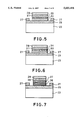
- FIG. 5 is a sectional structural view showing a light emitting device comprising oriented polycrystalline Ga 1-x In x N/n-Ga 1-x In x N/i-Ga 1-x In x N/p-Ga 1-x In x N.
- FIG. 6 is a sectional structural view showing a light emitting device comprising oriented polycrystalline Ga 1-x In x N/n-Ga 1-x In x N/P-Ga 1-y In y N/p-Ga 1-x In x N (x ⁇ y).
- FIG. 7 a sectional structural view showing a light emitting device comprising oriented polycrystalline Ga 1-a Al a N/n-Ga 1-a Al a N/p-Ga 1-b Al b N/p-Ga 1-a Al a N (a ⁇ b).
- FIG. 8 is a sectional structural view showing a light emitting device comprising oriented polycrystalline Ga 1-x-y In x Al y N/n-Ga 1-x-y In x Al y N/i-Ga 1-a-b In a Al b N/p-Ga 1-x-y In x Al y N.
- FIG. 9 is a sectional structural view showing a light emitting device comprising oriented polycrystalline GaN/n-GaN/n-GaN/p-GaN/n-Ga 1-x In x N/p-Ga 1-x In x N.
- FIG. 10 is a sectional structural view showing a light emitting device comprising GaInN composition graded structure/n-Ga 1-x In x N/p-Ga 1-x In x N.
- FIG. 11 is a sectional structural view showing a light emitting device comprising a strained super lattice structure/n-Ga 1-x In x N/p-Ga 1-x In x N.
- FIG. 12 is a sectional structural view showing a light emitting device comprising oriented polycrystalline Ga 1-x In x N/n-Ga 1-x In x N/a quantum well structure/p-Ga 1-x In x N.
- FIG. 13 is a sectional structural view showing a light emitting device comprising oriented polycrystalline Ga 1-x In x N/n-Ga 1-x In x N/p-Ga 1-x In x N/n-Ga 1-y In y N/p-Ga 1-y In y N.
- FIG. 14 is a schematic view showing a crystal growing apparatus used in producing thin films.
- FIG. 15 is a graph illustrating the diode-characteristics of a GaN light emitting device manufactured according to a first working example.
- FIG. 16 is a graph illustrating the emission spectrum of a GaN light emitting device made according to the first working example.
- FIG. 17 is a perspective view showing a cubic crystal system showing a crystal face inclined at an angle of ⁇ 2 to the (001) face towards the (100) face, and an angle of ⁇ 3 towards the (010) face.
- FIG. 18 is a perspective view showing a orthorhombic crystal system showing a face inclined at an angle of ⁇ 4 to the (001) face towards the (100) face.
- FIG. 19 is a sectional structural view showing a light detecting device comprising oriented polycrystalline Ga 1-x In x N/n-Ga 1-x In x N/i-Ga 1-x In x N/p-Ga 1-x In x N.
- the substrate according to the present invention With the substrate according to the present invention, at least one of the orientations of the periodic arrangement of the atoms on the surface of the substrate, and at least one of the orientations of the crystal axes of the lattice face of the first layer nitride semiconductor in direct contact with the substrate coincide, and the mismatch of an integer multiple (from 1 to 10) of the atomic spacing of the latter orientation and the atomic spacing of the former orientation is preferably within 5%.
- the atoms periodically arranged on the surface of the substrate are those atoms which occupy the lattice points of the substrate crystal, and are positioned uppermost on the crystal surface.
- the integer multiple of the atomic spacing in at least one direction of the lattice face of the nitride of the oriented polycrystalline nitride semiconductor of the first layer is from 1 to 10. If this exceeds 10 the stacking of the atoms exposed on the substrate surface, with the atomic orbits of the nitride semiconductor becomes small so that the crystal orienting function is decreased, making it difficult to obtain a well orientated polycrystalline nitride semiconductor layer.
- the difference between the integer multiple of the atomic spacing in at least one direction on the lattice face of the nitride of the oriented polycrystalline nitride semiconductor, and the atomic spacing of the periodic arrangement of the atoms on the surface of the substrate in the same direction is preferably within 5%. If the difference (or mismatch) is greater than this, it becomes difficult to obtain a well oriented nitride semiconductor layer. A mismatch value of less than 3% is more preferable, and less than 1% is even more preferable.
- mismatch between the atomic spacing of the substrate and that of the nitride semiconductor refers to the difference in atomic spacing between an atomic spacing (a) (in one direction) of the lattice face of the nitride semiconductor grown on the substrate surface and in contact with the substrate surface, and an atomic spacing (b) (in one direction) of the periodic arrangement of atoms on a specific cut face of the single crystal substrate.
- the magnitude of the mismatch is represented by
- /b ⁇ 100(%) where (n 1-10).
- the atomic spacing can be determined from the respective nitride semiconductor and the single crystal substrate lattice constants. This can be calculated once the substrate cut face has been decided.
- the atomic spacing mismatch between the integral multiple of the atomic spacing in a second direction of the lattice face of the nitride of the orientated polycrystalline nitride semiconductor of the first layer, and the atomic spacing of the periodic arrangement of atoms on the upper surface of the substrate in the same second direction is also within 5%.
- the form of the lattice face of the nitride of the orientated polycrystalline nitride semiconductor is preferably the same as that of the periodic arrangement of the atoms on the substrate surface.
- the following substrates may be used in the present invention.
- Single crystal semiconductor substrates such as Si, Ge, SiC, Group III-V compound semiconductor substrates such as GaAs, InAs, InP, and GaSb, and single crystal substrates such as AlN, ZnO, sapphire (Al 2 O 3 ), quartz (SiO 2 ), TiO 2 , MgO, MgF 2 , CaF 2 , and SrTiO 3 .
- the substrate crystal is grown so that a surface may be inclined at the desired angle to a predetermined reference face or cut and polished after growing the crystal.
- the lattice face is often about ⁇ 2 degrees out of alignment with the surface so that a complete lattice face generally does not occur on the surface.
- this type of substrate may also be used, it is preferable if a misalignment of not more than ⁇ 1 degrees exists and more preferable if this is less than ⁇ 0.5 degrees.
- a single crystal thin film which satisfies the above conditions is grown on generally used glass, polycrystalline substrate or single crystal substrate as a substrate.
- the required oriented polycrystalline nitride semiconductor can then be grown on top of this.
- a single crystal thin film for GaN, this may be a single crystal silicone substrate on which has been grown ZnO or SiC. There are no particular restrictions on the thickness of the single crystal thin film provided that a uniform surface is obtained.
- a transparent single crystal substrate having a transmissivity of not less than 80% in the wave length range from 360-800 mm. With this substrate, it is possible for emitted light or detected light to pass through the substrate.
- transparent single crystal substrates include sapphire, single crystal quartz, MgO, TiO 2 , MgF 2 , CaF 2 , and SrTiO 3 . Of these however the sapphire substrate is preferable.
- the C face (0001), R face (01 1 2), and A face (2 110) of the sapphire may be used as the lattice face, and the required substrate surface may be obtained by inclining at the required angle to these reference faces.
- the sapphire R face (01 1 2) is used, then with Ga 1-x In x N wherein x is in the range from 0 to 0.45, and Ga 1-y Al y N wherein y is in the range from 0 to 1, the difference in length between 3 times the length of the c-axis of the nitride semiconductor, and the axial length of the R face projection of the sapphire c-axis is within 5%. Consequently this is suitable as a substrate for the present invention.
- the thickness of the substrate of the present invention there are no particular limits to the thickness of the substrate of the present invention.
- the thickness when used as a light emitting device with light passing through the substrate, the thickness should preferably be as thin as possible.
- mechanical strength is the necessary consideration both in the manufacture of the nitride semiconductor thin film and in the manufacture of the subsequent device. Consequently a substrate thickness of from 0.05-2.0 mm is preferable. If this is less than 0.05 mm, mechanical strength is low making handling difficult. If the thickness is above 2.0 mm, then it becomes difficult to cut up the substrate for use as devices, and when used for light emitting devices, the light extraction efficiency is reduced.
- a feature of the present invention is that the nitride semiconductor layer grown directly on the substrate is an orientated polycrystalline nitride semiconductor layer having a thickness of not more than 5000 angstroms.
- the orientated polycrystalline nitride semiconductor layer in direct contact with the substrate at least one of the orientations of the periodic arrangement of atoms on the surface of the substrate, coincide with at least one of the orientations of the crystal axis of the lattice face of the first layer nitride semiconductor layer in direct contact with the substrate.
- mismatch of an integer multiple (from 1 to 10) of the atomic spacing of the latter orientation, and the atomic spacing of the former orientation is within 5%.
- the crystal grows two dimensionally, and aligns itself in a direction for minimum mismatch. Moreover, crystallinity of the thin film improves with increasing distance from the substrate surface.
- the crystal of the nitride semiconductor may be aligned parallel with the substrate surface, so that a smooth surface is possible. Consequently an operating layer having good characteristics may be grown on top of this layer.
- This phenomena wherein orientation is improved may be observed during semiconductor thin film growth by Refractive High Energy Electron Diffraction (RHEED) techniques. It may also be observed after growth of the thin film by transmission electron microscope or X-ray diffraction methods.
- RHEED Refractive High Energy Electron Diffraction
- the thickness of the oriented polycrystalline nitride semiconductor layer is less than 5000 angstroms, this depends on the film growth rate and degree of mismatch. When the film growth rate or mismatch are large, a thick orientated polycrystalline nitride semiconductor film is not obtained and the single crystal nitride semiconductor tends to grow with a rough surface.
- the oriented polycrystalline nitride semiconductor layer is made using the Molecular Beam Epitaxy (MBE) method according to the present invention, a thickness of less than 5000 angstroms gives adequate device characteristics. If the thickness of the thin film is greater than this, the growth time of the thin film becomes excessive so as to be unpractical.
- MBE Molecular Beam Epitaxy
- the film thickness of the oriented polycrystalline nitride semiconductor layer should preferably be within the range of from 10-5000 angstroms.
- the oriented polycrystalline nitride semiconductor layer of the present invention may comprise nitrogen and at least one Group III constituent selected from Al, Ga, or In.
- the resultant structure is such that the direction of the c-axis of the nitride semiconductor on the sapphire R face is aligned with the axial direction of the projection of the sapphire c-axis on the R face.
- the thickness of the layer depends on the film growth rate and is normally from 300-2500 angstroms.
- the nitride semiconductor composition is given a composition graded structure with the structure changing gradually from the substrate side to finally give a required operating layer composition.
- the composition graded structure involves growing a semiconductor thin film comprising Ga 1-x-y In x Al y N (0 ⁇ x ⁇ 1, 0 ⁇ y ⁇ 1) on the substrate so as to give the finally required operating layer structure.
- the Ga 1-x-y In x Al y N (0 ⁇ x ⁇ 1, 0 ⁇ y ⁇ 1) composition the x and/or y value may change gradually from the substrate side.
- This change may be determined by consideration of the required operating layer properties, and may involve changing the composition to increase the lattice constant, or changing the composition to decrease the lattice constant.
- this composition graded structure the stress applied to the operating layer may be minimized even in cases where defects exist in the crystal. Consequently device characteristics and durability may be improved.
- a plurality of oriented polycrystalline nitride semiconductor layers having a composition different from that of the nitride semiconductor and a thickness of less than 100 angstroms are arranged in alternately stacked layers.
- the characteristics and durability of the device may be improved. In this case the effectiveness is reduced if the thickness of the respective layers is too thick. Consequently the thickness should be less than 100 angstroms, preferably less than 70 angstroms and more preferably less than 50 angstroms.
- the thickness of the oriented polycrystalline nitride semiconductor layer should be not less than 10 angstroms. If less than this, the beneficial effect on device characteristics and durability does not appear.
- the flatness of the surface of the oriented polycrystalline nitride semiconductor obtained in this way has an unevenness of less than 100 angstroms. With this surface it thus possible to grow a second layer having good crystallization. This amount of unevenness can be measured by means of an atomic force microscope.
- the oriented polycrystalline nitride semiconductor layer formed in direct contact with the substrate surface has good electrical conductivity. Hence a uniform electric field may be applied over the entire operating layer by appropriate connection to terminals for operation of the device.
- n-type or p-type doping may be performed.
- dopants such as Si, Ge, C, Sn, Se, Te and the like may be used.
- carrier density may be controlled, and electrical resistance reduced.
- the carrier density should be not less than 10 17 cm -3 , and preferably not less than 10 18 cm -3 .
- the single crystal nitride semiconductor according to the present invention may comprise a constituent containing nitrogen and at least one Group III constituent selected from Al, Ga or In.
- the band gap of these constituents lies within the broad range of from 2.4 eV for InN, 3.4 eV for GaN, to 6.2 eV for AlN.
- Band gap control may be achieved by making a mixed crystal semiconductor thin film comprising Al, Ga, or In. For example, this may comprise AlGaN, GaInN, or AlGaInN.
- band gap control may be achieved by doping the semiconductor or mixed crystal semiconductor with a p-type or n-type dopant.
- the operating layer of single crystal nitride semiconductor formed on the substrate may comprise one or two groups of single crystal nitride semiconductor layer having at least one n-type, i-type or p-type single crystal nitride semiconductor layer, depending upon the purpose of the device.
- the n-type dopant may be, Si, Ge, C, Sn, Se, Te and the like
- the p-type dopant or i-type dopant may be Mg, Ca, Sr, Zn, Be, Cd, Hg, or Li and the like.
- the type of dopant and the amount used the required conductivity type and carrier density may be obtained.
- a structure may be made with a variation in doping concentration in the direction of the film thickness, and a structure with a ⁇ doping layer with doping only in a specific layer may also be obtained.
- the oriented polycrystalline nitride semiconductor according to the present invention is able to distinguish from the single crystal nitride semiconductor and the polycrystalline nitride semiconductor by using a multiple axis X-ray diffraction, or a transmission electron microscope method, or an electron beam diffraction method.
- the nitride semiconductor devices may be for example; field effect transistors wherein the majority-carrier flow in the n-type or p-type nitride semiconductor layer is controlled by applying a voltage to the gate, bi-polar transistors having an n-p-n-type or p-n-p-type nitride semiconductor layer structure, light emitting devices having a structure comprising at least one n-type, p-type or i-type nitride semiconductor layer, light detecting devices with a structure comprising an n-type/p-type/i-type nitride semiconductor layer, rectifying devices with a structure comprising a p + -type/n-type/n + -type nitride semiconductor layer, light emitting devices or electronic elements with a structure combining n-type and/or p-type with a quantum well structure.
- the nitride compound semiconductor devices of the present invention are not limited to those of the above.
- FIGS. 2 to 13 show examples of structures of operating layers for use as a light emitting devices.
- a single crystal (n-GaN) 25/single crystal (p-GaN) 26 is formed on an oriented polycrystalline (GAN) 24 which is formed on the substrate 23.
- a terminal 27 is connected to the oriented polycrystalline (GAN) 24, and a terminal 28 is formed on the operating layer 26.
- a single crystal (n-Ga 1-x In x N) 30/single crystal (p-Ga 1-x In x N) 31 is formed on an oriented polycrystalline (Ga 1-x In x N) 29 which is formed on the substrate 23.
- a terminal 27 is formed on the oriented polycrystalline (Ga 1-x In x N) 29, and a terminal 28 is formed on the operating layer 31.
- an n-GaN/i-GaN, n-Ga 1-x Al x N/p-Ga 1-x Al x N/p-Ga 1-x Al x N operating layer is possible as well as the structures of FIGS. 4 to 13.
- n-GaN single crystal
- p-GaN single crystal
- p-GaN single crystal
- p-GaN single crystal
- n + -GaN oriented polycrystalline
- a terminal 27 is formed on the oriented polycrystalline (n + -GaN) 32, and a terminal 28 is formed on the operating layer 26.
- a terminal 27 is formed on the oriented polycrystalline (Ga 1-x In x N) 29, and a terminal 28 is formed on the operating layer 31.
- a terminal 27 is formed on the oriented polycrystalline (Ga 1-x In x N) 29, and a terminal 28 is formed on the operating layer 31.
- a terminal 27 is formed on the oriented polycrystalline (Ga 1-a Al a N) 35, and a terminal 28 is formed on the operating layer 38.
- a terminal 27 is formed on the oriented polycrystalline (Ga 1-x-y In x Al y N) 39, and a terminal 28 is formed on the operating layer 42.
- a single crystal (n-GaN) 25/single crystal (p-GaN) 26/single crystal (n-Ga 1-x In x N) 30/single crystal (p-Ga 1-x In x N) 31, is formed on an oriented polycrystalline GaN 24 which is formed on the substrate 23.
- respective terminals 27, 28 and 43 are formed on the oriented polycrystalline GaN 24, the single crystal (p-GaN) 26, and the single crystal (n-Ga 1-x In x N) 30, and a terminal 44 is formed on the single crystal (p-Ga 1-x In x N) 31 of the operating layer.
- a single crystal (n-Ga 1-x In x N) 30/single crystal (p-Ga 1-x In x N) 31, is formed on a GaInN composition graded structural layer 45 which is formed on the substrate 23.
- a terminal 27 is formed on the composition graded structural layer 45, and a terminal 28 is formed on the operating layer 31.
- a single crystal (n-Ga 1-x In x N) 30/single crystal (p-Ga 1-x-y In x N) 31 is formed on the strained super lattice structural layer 49 which is formed on the substrate 23.
- a terminal 27 is formed on the strained super lattice structural layer 49, and a terminal 28 is formed on the operating layer 31.
- a single crystal (n-Ga 1-x In x N) 30/quantum well layer 46/single crystal (p-Ga 1-x In x N) 31, is formed on an oriented polycrystalline (Ga 1-x In x N) 29 which is formed on the substrate 23.
- a terminal 27 is formed on the oriented polycrystalline (Ga 1-x In x N) 29, and a terminal 28 is formed on the operating layer 31.
- the quantum well structure comprises an active layer of the nitride semiconductor layer of less than several hundred angstroms thick in order to obtain the quantum effect, sandwiched between wider band gap nitride semiconductor cladding layers.
- This type of structure involves a single quantum well structure. If this is stacked with a thin barrier layer in between to make a multiple quantum well structure, the light emission efficiency may be increased, and the emitted light threshold value current may be reduced.
- the light emitting layer has two layers.
- a single crystal (n-Ga 1-x In x N) 30/single crystal (p-Ga 1-x In x N) 31/single crystal (n-Ga 1-y In y N) 47/single crystal (p-Ga 1-y In y N) 34 is formed on an oriented polycrystalline (Ga 1-x In x N) 29 which is formed on the substrate 23.
- respective terminals 27, 28 and 43 are formed on the oriented polycrystalline (Ga 1-x In x N) 29, the single crystal (p-Ga 1-x In x N) 31 and the single crystal (n-Ga 1-y In y N) 47, and a terminal 44 is formed on the single crystal (p-Ga 1-y In y N) 34 of the operating layer.
- a voltage is applied for example between the terminals 27 and 28, a blue light is emitted, if the voltage is applied between the terminals 43 and 44 a green light is emitted, while if the voltage is applied between the terminals 27 and 44 a yellow light is emitted.
- the film thickness of the operating layer of the single crystal nitride semiconductor should be thin in order to facilitate the etching process.
- a thickness of less than 5 microns is preferable and more preferably less than 3 microns.
- the operating layer should be made thin in order to improve the light output emission efficiency.
- the thickness should be less than 3 microns, and in particular with short wavelength light emitting devices, the operating layer should be as thin as possible due to the susceptibility to light absorption.
- the layer should be thick enough to ensure that a tunnel current flow does not occur. Hence the thickness should be at least 100 angstroms thick.
- the thickness should be no more than 5000 angstroms. If the thickness is greater than this, current flow becomes difficult so that use as a light emitting device is not possible.
- MIS metal insulator semiconductor
- the thickness of both the p-type and n-type single crystal nitride semiconductors operating layers is no more than 3 microns thick. With greater film thickness growth time becomes excessive making device production impractical. Also efficiency in extraction of the emitted light is reduced.
- a surface layer of p-type or i-type single crystal nitride semiconductor is necessary with terminals formed on this surface layer.
- efficient extraction of the light emitted in the operating layer is possible from the substrate side, it is also possible to remove this light from the surface layer side.
- the terminal formed in a pattern to ensure a uniform voltage distribution over the surface layer should cover no more than 50% of the surface area.
- the light should be taken from the terminal side rather than having to pass through the thick substrate layer. Hence if the terminal covers more than 50% of the surface layer, light extraction efficiency is reduced.
- the terminal pattern may comprise shapes such as a comb shape, a meandering shape or a net shape.
- the material used for the terminal for applying a voltage to the surface of the nitride semiconductor may be a simple metal such as Al, In, Cu, Ag, Au, Pt, Ir, Pd, Rh, W, Ti, Ni, Co, Sn, or Pb. Alternatively alloys of these metals or silicides of Pt, W, or Mo and the like may be used. Moreover, stannic oxide, indium oxide, stannic oxide-indium oxide, or degenerated ZnSe and the like may be used. Of particular suitability for the terminal formed on the n-type nitride semiconductor are the simple metals such as Al, In, Ti, Cu, Zn, Co, Ag, Sn or Pb, or alloys of these.
- the pattern used for the terminals on the p-type or i-type nitride semiconductor should preferably be a meander type, net type or comb type pattern.
- the width and spacing between the terminals may be varied depending on the magnitude of the electrical resistance and imprinted voltage related to the p-type or i-type semiconductor layer. Reducing the width of the terminal and the terminal spacing may enhance the light extraction efficiency for the situation where the light is extracted through the terminals.
- a crystal growth apparatus having a gas source for the supply of a compound including nitrogen in a gaseous state, and a solid body source for the supply of Group III constituents is used.
- the gaseous state compound including nitrogen, and the Group III constituents are supplied to the substrate surface with the substrate at a temperature of 300° C.-1000° C. under a pressure of less than 10 -5 Torr. Under these conditions, a first layer is grown on the substrate surface at a growth rate of 0.10-20 angstroms per second.
- the gaseous state compound including nitrogen, and the Group III constituent are supplied to the surface of the first layer at a substrate temperature of 300° C.-1000° C. under a pressure of less than 10 -5 Torr, and a single crystal nitride semiconductor layer is grown at a growth rate of 0.10-10 angstroms per second, thereby forming a nitride semiconductor device.
- the compound including nitrogen may be one of ammonia, nitrogen triflouride, hydrazine or dimethylhydrazine.
- a gas mixture with these as the principal constituents may be used.
- the ammonia, nitrogen triflouride, hydrazine, or dimethylhydrazine may be diluted with nitrogen, or an inert gas such as argon or helium.
- a gas cell may be used to supply this gas. This may be provided in the crystal growth apparatus with an opening facing the substrate.
- the shape of the opening may be for example a nozzle shape, a slit shape or consist of perforations.
- the gas supply equipment should preferably comprise a valve and flow control device fitted to piping connected to the gas cell opening, with a pressure regulator connected so that the mixture and supply quantity of the above gases may be controlled, and the supply may be turned on and off. Furthermore, in order to produce high quality nitride semiconductor thin films, it should be possible to heat the nitrogen containing compound for supply to the substrate surface by heating the gas cell to a predetermined temperature. To efficiently heat the gas cell, materials having high corrosion resistance such as alumina, silica, boron nitride, silicone carbide may be used in a fibrous, flaked, crushed or granular form.
- the contact surface area provided for the gaseous state compound in the gas cell may be increased thereby improving heating efficiency. It is necessary to change the heating temperature depending on the type of filler material in the gas cell, and the supply amount of nitrogen containing compounds. Preferably the temperature should be set within the range from 100° C.-700° C. Furthermore, it is possible to use a plasma gas cell to activate the nitrogen or ammonia supplied to the substrate surface. The amount of gaseous compound supplied to the substrate surface should be greater than that of the Group III constituents.
- the supply amount of gaseous state compound should be at least 10 times, preferably 100 times, and more preferably 1000 times the supply amount for the Group III constituents.
- the pressure during growing should be not greater than 10 -5 Torr. This is so that the gaseous state nitrogen containing compound, and the metal vapor, both necessary for growth of the nitride semiconductor thin film reach the substrate surface without colliding with each other. If the pressure is above 10 -5 Torr the impurities within the growing chamber become excessive and reaction may occur before reaching the substrate surface, making it difficult to obtain a nitride semiconductor thin film having good crystallization. It is particularly important to ensure that impurities such as compounds containing carbon or oxygen are kept to a minimum. In this respect, by suppressing the partial pressures of carbon monoxide and carbon dioxide, the amount of oxygen and carbon diffusing into the nitride semiconductor thin film may be kept to a minimum. Accordingly the partial pressure of carbon monoxide and carbon dioxide should be kept to below 10 -8 Torr and more preferably below 10 -10 Torr. The type and concentration of the gas impurities may be measured by means of a quadrupole mass spectrometer.
- the growth temperature for the nitride semiconductor thin film is 300° C.-1000° C. However, within this range, the composition of the nitride semiconductor thin film may be changed by the type of nitrogen containing compound used, the doping material and the growth rate.
- the growth rate of the nitride semiconductor thin film of the present invention should be from 0.1-20 angstroms per second. With a growth rate of less than 0.1 angstroms per second, an excessively long growth time is necessary to obtain the required film thickness. Consequently an excessive amount of impurities from the growth atmosphere enter the film, making it difficult to produce a good quality nitride semiconductor thin film. With a growth rate greater than 20 angstroms per second, island type growth occurs so that a good quality nitride semiconductor thin film is not possible.
- the growth rate For growing an oriented polycrystalline nitride semiconductor thin film, the growth rate should be from 0.1-20 angstroms per second, and for the subsequent growth of a single crystal nitride semiconductor thin film on the oriented polycrystalline nitride semiconductor layer, the growth rate should be from 0.1-10 angstroms per second. Growth rate may be controlled by changing the amount of the principal Group III constituent supplied to the substrate surface. This may be achieved by adjusting the temperature of the crucible used for evaporating the Group III constituent. Growth rate may also be controlled by changing the nitrogen containing compound supply rate, and by changing the substrate temperature.
- the Group III simple or alloy metals or metal salts may be used for providing the Group III constituent.
- At least one of the Group III constituents may be selected aluminum, gallium and indium.
- carrier density control, and p-type, i-type or n-type conduction type control may be achieved by impurity doping.
- a doping impurity such as Mg, Ca, St, Zn, Be, Cd, Hg or Li may be used.
- the carrier type and carrier density may be changed by changing the amount of Si used as the doping impurity. In this case, the doping concentration in the direction of the film thickness may be changed, and the ⁇ doping method for doping only a specific layer may be used.
- Conduction type control may also be promoted by irradiating with an electron beam or ultraviolet rays during doping. Furthermore, on completion of the stacked layer construction, electron beamed irradiation and heat treatment may be used to improve the p-type efficiency.
- the nitrogen containing compound and the Group III constituent may be supplied to the substrate surface simultaneously, or successively.
- the thin film growth may be interrupted and the thin film subjected to a method to promote crystallization. It may be preferable during thin film growth to observe that the streak observable by the RHEED pattern is visible.
- the equipment used comprises a crystal growth apparatus fitted with a vacuum chamber 1 housing evaporation crucibles (Knudsen cells) 2, 3, 4, 5 and 6, a gas cell 7, a substrate heating holder 8 on which is mounted a substrate 9.
- Other equipment includes a quadrupole mass spectrometer 10, a RHEED electron gun 11, a RHEED screen 12, a shroud 13, shutters 14-18, a valve 19, a cold trap 20, a diffusion pump 21 and an oil-sealed rotary vacuum pump 22.
- Gallium metal is placed in the evaporation crucible 2 and heated to a temperature suitable for a growth rate on the substrate surface of 10 13 -10 17 /cm 2 second.
- Ammonia is introduced through the gas cell 7 so as to impinge directly onto the substrate 9.
- a sufficient amount is supplied so as to produce a growth rate of 10 16 -10 20 /cm 2 sec. on the substrate service.
- Indium, aluminum, arsenic, or tin and the like are placed in the evaporation crucibles 3 and 4, and the temperature and supply time controlled so as to grow a mixed crystal compound semiconductor of a predetermined composition.
- Magnesium, calcium, strontium, zinc, beryllium, cadmium, mercury and lithium and the like are placed in the evaporation crucible 5 while silicon, germanium, carbon, tin, sulfur, selenium and tellurium and the like are placed in the evaporation crucible 6. Doping is then performed by adjusting the temperature and supply time to give a predetermined supply amount.
- the R face of sapphire is used as the substrate 9 and this is heated within the range of 300° C. to 900° C.
- the substrate 9 is heated in the vacuum chamber 1 to a temperature of 900° C.
- a predetermined growth temperature is then set and a layer of oriented polycrystalline nitride semiconductor having a thickness ranging from 10-500 angstroms is grown at a growth rate of 0.1-20 angstroms per second.
- Evaporation crucible 6 may be used for n-type doping to improve conductivity in the nitride semiconductor layer.
- an n-type single crystal nitride semiconductor layer of a thickness from 0.05-3 microns may be formed on the nitride semiconductor layer at a growth rate of 0.1-10 angstroms per second.
- nitride semiconductor doped with p-type or i-type dopant may be grown on the n-type single crystal nitride semiconductor layer, thereby fabricating a laminated structure nitride semiconductor.
- the shape of the device together with the terminals for applying current to the element is defined by using a lithographic process on the laminated structure.
- the lithographic process involves the use of standard photoresist materials. Dry etching is preferably used in the etching process. In the dry etching process, standard processes involving ion milling, ECR etching, reactive ion etching, ion beam assisted etching, and focused ion beam etching may be used.
- the present invention has the advantage that since the overall film thickness of the nitride semiconductor laminated thin film is small, the dry etching process may be most effectively applied.
- the nitride semiconductor laminated thin film is damaged by the dry etching process, then by heat treating in an atmosphere of the nitrogen containing compound of the present invention, or nitrogen or an inert gas such as argon or helium an device having even better properties can be obtained.
- the heat treatment temperature and period may be changed to suit the composition and structure of the nitride semiconductor of the device. For example, with a GaN light emitting device, heat treatment at 500° C. for 30 minutes in a flow of ammonia is sufficient to restore damage to the surface due to etching.
- the terminals used for applying a uniform voltage to the surface of the nitride semiconductor may be produced by the MBE method, CVD method, vacuum evaporation method, electron beam evaporation method, or by sputtering.
- the pattern used for the terminals on the p-type or i-type nitride semiconductor should preferably be a meander type, net type or comb type pattern.
- the width and spacing between the terminals may be varied depending on the magnitude of the electrical resistance and imprinted voltage related to the p-type or i-type semiconductor layer. Reducing the width of the terminal and the terminal spacing may enhance the light extraction efficiency for the situation where the light is extracted through the terminals.
- the heat treatment temperature and period may be changed depending on the terminal material and structure. For example, with an MIS type GaN light emitting device using Al in an n-type nitride semiconductor and Au in an i-type nitride semiconductor, heat treatment at 400° C. for 60 minutes in a flow of argon gas results in an excellent metal/semiconductor contact.
- the laminated structure produced by the above method may be cut by a dicing saw to give the device chip. Subsequently, after setting in a lead frame, wiring using gold leads or aluminum leads may be attached using a die bonding method and/or a wire bonding method. The device may then be packaged using epoxy resin, metallic resin or carbonate resin to give a light emitting device.
- a crystal growing apparatus comprising evaporation crucibles 2, 3, 4, 5, 6, a gas cell 7 and a substrate heating holder 8 housed inside a vacuum chamber 1 is used.
- a charge of gallium metal is placed in the evaporation crucible 2 and heated to a temperature of around 1020° C.
- a charge of zinc is placed in the evaporation crucible 5 and heated to a temperature of around 190° C.
- Gas is supplied by the gas cell 7 which is filled with alumina fiber. The gas is heated to a temperature of 370° C. by the gas cell 7 and directed onto the substrate 9 at a flow rate of 5 cc/minute.
- a sapphire R face substrate is used for the substrate 9.
- the atomic spacing forming the line of intersection of the A and C faces of the GaN differs from the sapphire substrate atomic spacing by 15.7%, and three times the C-axis length of the GaN differs from the sapphire substrate atomic spacing by 0.7%.
- the vacuum chamber is evacuated to a pressure of 2 ⁇ 10 -6 Torr for growing the thin film.
- the substrate 9 is first heated and held at a temperature of approximately 900° C. for 30 minutes. The temperature is then lowered to 750° C. for growing the thin film. To grow the thin film, the shutter of the gallium crucible 2 is opened while supplying a stream of ammonia gas from the gas cell 9 to the substrate. As a result, a thin film of multiply oriented crystalline GaN approximately 1000 Angstroms thick is deposited on the substrate surface at a film growth rate of approximately 1.2 Angstroms/second. The temperature of crucible 2 is then raised to 1010° C., and a 3500 Angstroms thick layer of single crystal n-GaN is deposited at a film growth rate of approximately 1.0 Angstroms/second.
- a single crystal layer of p-GaN doped with zinc is deposited to a thickness of 500 Angstroms, thereby producing a nitride semiconductor laminated structure.
- a terminal for supplying current to the device is then formed on the laminated thin film by a lithographic process. This may involve the use of standard photoresist materials.
- the n-GaN layer and the p-GaN layer may be removed by ion milling with argon to form the spaces for the pattern of the terminal used to apply a voltage to the device.
- the device is heat treated in ammonia gas at 500° C. for 30 minutes.
- a resist pattern for the terminals is then applied, and a 3000 Angstroms thick aluminum terminal layer deposited on the multiply oriented crystalline GaN layer, and a 3000 Angstroms thick gold layer deposited on the p-GaN layer using the vacuum deposition method.
- the device is then heat treated in Argon gas at 400° C. for 60 minutes.
- the laminated structure formed in this way was then cut up with a dicing saw and wired with gold wire using a wire bonder.
- the device structure of the present invention is shown in FIG. 2, while the measured results of diode characteristics, and emitted light spectrum are shown in FIGS. 15 and 16 respectively.
- This device gave a blue light emission having a wave length of 470 nm and intensity of 90 mcd when a current of 20 mA was supplied to the device.
- Example 2 a crystal growing apparatus the same as that used in Example 1 is used. At first a charge of gallium metal is placed in the evaporation crucible 2 and heated to a temperature of around 1020° C., and a charge of Mg is placed in the evaporation crucible 5 and heated to a temperature of around 280° C. Gas is supplied by the gas cell 7 which is filled with alumina fiber. The gas is heated to a temperature of 370° C. by the gas cell 7 and directed onto the substrate 9 at a flow rate of 5 cc/minute.
- a sapphire R face substrate is used for the substrate 9.
- the vacuum chamber is evacuated to a pressure of 2 ⁇ 10 -6 Torr for growing the thin film.
- the substrate 9 is first heated and held at a temperature of approximately 900° C. for 30 minutes. The temperature is then lowered to 750° C. for growing the thin film. To grow the thin film, the shutter of the gallium evaporation crucible 2 is opened while supplying a stream of ammonia gas from the gas cell 7 to the substrate. As a result, a thin film of multiply oriented crystalline GaN approximately 1000 Angstroms thick is deposited on the substrate surface at a film growth rate of approximately 1.2 Angstroms/second.
- the temperature of crucible 2 is then raised to 1010° C., and a 3500 Angstroms thick layer of single crystal n-GaN is deposited at a film growth rate of approximately 1.0 Angstroms/second. Subsequently, the crucible 2 shutter and the Mg crucible 5 shutter are opened together, and a single crystal layer of i-GaN doped with Mg is deposited to a thickness of 500 Angstroms, thereby producing a nitride semiconductor laminated structure.
- the laminated thin film was then made into a light emitting device using methods similar to those used for Example 1.
- This device gave a purple light emission having a wave length of 430 nm and an intensity of 5 mcd when a current of 20 mA was supplied to the device.
- a charge of gallium metal is placed in the evaporation crucible 2 and heated to a temperature of around 1020° C.
- a charge of In is placed in the evaporation crucible 3 and heated to a temperature of around 820° C.
- a charge of Mg is placed in the evaporation crucible 5 and heated to a temperature of around 280° C.
- Ammonia gas is used in the process. This is supplied by the gas cell 7 which is filled with alumina fiber. The ammonia gas is heated to a temperature of 370° C. by the gas cell 7 and directed onto the substrate 9 at a flow rate of 5 cc/minute.
- a sapphire R face substrate is used for the substrate 9.
- the atomic spacing forming the line of intersection of the A and C faces of the Ga 0 .9 In 0 .1 N differs from the sapphire substrate atomic spacing by 16.0%, and three times the C-axis length of the Ga 0 .9 In 0 .1 N differs from the sapphire substrate atomic spacing by 1.8%.
- the vacuum chamber is evacuated to a pressure of 2 ⁇ 10 -6 Torr for growing the thin film.
- the substrate 9 is first heated and held at a temperature of approximately 900° C. for 30 minutes. The temperature is then lowered to 700° C. for growing the thin film. To grow the thin film, the shutters of the gallium evaporation crucible 2 and the In evaporation crucible 3 are opened together while supplying a stream of ammonia gas from the gas cell 9 to the substrate. As a result, a thin film of multiply oriented crystalline Ga 0 .9 In 0 .1 N approximately 1700 Angstroms thick is deposited on the substrate surface at a film growth rate of approximately 1.3 Angstroms/second.
- the temperature of crucible 2 is then raised to 1010° C., and the temperature of crucible 3 raised to a temperature of 800° C., and a 3500 Angstroms thick layer of single crystal n-Ga 0 .9 In 0 .1 N is deposited at a film growth rate of approximately 1.0 Angstroms/second.
- the crucible 2 shutter and the Mg crucible 5 shutter are opened together, and an i-single crystal Ga 0 .9 In 0 .1 N layer doped with Mg is deposited to a thickness of 500 Angstroms, thereby producing a nitride semiconductor laminated structure.
- the laminated thin film was then made into a light emitting device using methods similar to those used for Example 1.
- This device gave a blue light emission having a wave length of 480 nm and an intensity of 50 mcd when a current of 20 mA was supplied to the device.
- a charge of gallium metal is placed in the evaporation crucible 2 and heated to a temperature of around 1020° C.
- a charge of In is placed in the evaporation crucible 3 and heated to a temperature of around 880° C.
- a charge of Mg is placed in the evaporation crucible 5 and heated to a temperature of around 280° C.
- Ammonia gas is used in the process. This is supplied by the gas cell 7 which is filled with alumina fiber. The ammonia gas is heated to a temperature of 370° C. by the gas cell 7 and directed onto the substrate 9 at a flow rate of 5 cc/minute.
- a sapphire R face substrate is used for the substrate 9.
- the atomic spacing forming the line of intersection of the A and C faces of the Ga 0 .7 In 0 .3 N differs from the sapphire substrate atomic spacing by 16.7%, and three times the C-axis length of the Ga 0 .7 In 0 .3 N differs from the sapphire substrate atomic spacing by 4.3%.
- the vacuum chamber is evacuated to a pressure of 2 ⁇ 10 -6 Torr for growing the thin film.
- the substrate 9 is first heated and held at a temperature of approximately 900° C. for 30 minutes. The temperature is then lowered to 680° C. for growing the thin film. To grow the thin film, the shutters of the gallium evaporation crucible 2 and the In evaporation crucible 3 are opened together while supplying a stream of ammonia gas from the gas cell 9 to the substrate. As a result, a thin film of multiply oriented crystalline Ga 0 .9 In 0 .3 N approximately 1700 Angstroms thick is deposited on the substrate surface at a film growth rate of approximately 1.5 Angstroms/second.
- the temperature of crucible 2 is then raised to 990° C., and the temperature of crucible 3 raised to a temperature of 840° C., and a 3500 Angstroms thick layer of single crystal n-Ga 0 .7 In 0 .3 N is deposited at a film growth rate of approximately 1.0 Angstroms/second.
- the crucible 2 shutter and the Mg crucible 5 shutter are opened together, and an i-single crystal Ga 0 .7 In 0 .3 N layer doped with Mg is deposited to a thickness of 500 Angstroms, thereby producing a nitride semiconductor laminated structure.
- the laminated thin film was then made into a light emitting device using methods similar to those used for Example 1.
- This device gave a green light emission having a wave length of 540 nm and an intensity of 70 mcd when a current of 20 mA was supplied to the device.
- a charge of gallium metal is placed in the evaporation crucible 2 and heated to a temperature of around 1020° C.
- a charge of Al is placed in the evaporation crucible 4 and heated to a temperature of around 1070° C.
- a charge of Mg is placed in the evaporation crucible 5 and heated to a temperature of around 280° C.
- Ammonia gas is used in the process. This is supplied by the gas cell 7 which is filled with alumina fiber. The ammonia gas is heated to a temperature of 370° C. by the gas cell 7 and directed onto the substrate 9 at a flow rate of 5 cc/minute.
- a sapphire R face substrate is used for the substrate 9.
- the atomic spacing forming the line of intersection of the A and C faces of the Ga 0 .7 Al 0 .3 N differs from the sapphire substrate atomic spacing by 14.5%, and three times the C-axis length of the Ga 0 .7 In 0 .3 N differs from the sapphire substrate atomic spacing by 0.9%.
- the vacuum chamber is evacuated to a pressure of 2 ⁇ 10 -6 Torr for growing the thin film.
- the substrate 9 is first heated and held at a temperature of approximately 900° C. for 30 minutes. The temperature is then lowered to 8° C. for growing the thin film. To grow the thin film, the shutters of the gallium evaporation crucible 2 and the In evaporation crucible 3 are opened together while supplying a stream of ammonia gas from the gas cell 9 to the substrate. As a result, a thin film of multiply oriented crystalline Ga 0 .7 In 0 .3 N approximately 1900 Angstroms thick is deposited on the substrate surface at a film growth rate of approximately 1.5 Angstroms/second.
- the temperature of crucible 2 is then raised to 990° C., and the temperature of crucible 3 raised to a temperature of 10° C., and a 3500 Angstroms thick layer of single crystal n-Ga 0 .7 Al 0 .3 N is deposited at a film growth rate of approximately 1.0 Angstroms/second.
- the crucible 2 shutter and the Mg crucible 5 shutter are opened together, and an i-single crystal Ga 0 .7 In 0 .3 N layer doped with Mg is deposited to a thickness of 500 Angstroms, thereby producing a nitride semiconductor laminated structure.
- the laminated thin film was then made into a light emitting device using methods similar to those used for Example 1.
- This device gave a purple light emission having a wave length of 370 nm and a power of 0.5 mW when a current of 20 mA was supplied to the device.
- a charge of gallium metal is placed in the evaporation crucible 2 and heated to a temperature of around 1020° C.
- a charge of Zn is placed in the evaporation crucible 5 and heated to a temperature of around 190° C.
- Ammonia gas is used in the process. This is supplied by the gas cell 7 which is filled with alumina fiber. The ammonia gas is heated to a temperature of 370° C. by the gas cell 7 and directed onto the substrate 9 at a flow rate of 5 cc/minute.
- the sapphire face shown in FIG. 1 inclined at 9.2 degrees to the R face towards the A face is used for the substrate 9.
- four times the atomic spacing forming the line of intersection of the A and C faces of the GaN differs from the sapphire substrate atomic spacing by 1.0%
- three times the C-axis length of the GaN differs from the sapphire substrate atomic spacing by 0.7%.
- the vacuum chamber is evacuated to a pressure of 2 ⁇ 10 -6 Torr for growing the thin film.
- the substrate 9 is first heated and held at a temperature of approximately 900° C. for 30 minutes. The temperature is then lowered to 750° C. for growing the thin film. To grow the thin film, the shutter of the gallium crucible is opened while supplying a stream of ammonia gas from the gas cell 9 to the substrate. As a result, a thin film of multiply oriented crystalline GaN approximately 1000 Angstroms thick is deposited on the substrate surface at a film growth rate of approximately 1.2 Angstroms/second. The temperature of crucible 2 is then raised to 1010° C., and a 4000 Angstroms thick layer of single crystal n-GaN is deposited at a film growth rate of approximately 1.0 Angstroms/second.
- a single crystal p-GaN layer doped with Zn is deposited to a thickness of 500 Angstroms, thereby producing a nitride semiconductor laminated structure.
- the laminated thin film was then made into a light emitting device using methods similar to those used for Example 1.
- This element gave a blue light emission having a wave length of 470 nm and an intensity of 110 mcd when a current of 20 mA was supplied to the device.
- a crystal growing apparatus the same as that used in Example 1 is used. At first a charge of gallium metal is placed in the evaporation crucible 2 and heated to a temperature of around 1020° C., and a charge of Zn is placed in the evaporation crucible 5 and heated to a temperature of around 190° C. Ammonia gas is used in the process. This is supplied by the gas cell 7 which is filled with alumina fiber. The ammonia gas is heated to a temperature of 370° C. by the gas cell 7 and directed onto the substrate 9 at a flow rate of 5 cc/minute.
- the face inclined at 20.2 degrees to the sapphire (10 1 0) face towards the C face is used for the substrate 9.
- one times the atomic spacing forming the line of intersection of the A and C faces of the GaN differs from the sapphire substrate atomic spacing by 33.2%, and eight times the C-axis length of the GaN differs from the sapphire substrate atomic spacing by 0.5%.
- the vacuum chamber is evacuated to a pressure of 2 ⁇ 10 -6 Torr for growing the thin film.
- the substrate 9 is first heated and held at a temperature of approximately 900° C. for 30 minutes. The temperature is then lowered to 750° C. for growing the thin film. To grow the thin film, the shutter of the gallium crucible is opened while supplying a stream of ammonia gas from the gas cell 9 to the substrate. As a result, a thin film of multiply oriented crystalline GaN approximately 4600 Angstroms thick is deposited on the substrate surface at a film growth rate of approximately 1.2 Angstroms/second. The temperature of crucible 2 is then raised to 1010° C., and a 4000 Angstroms thick layer of single crystal n-GaN is deposited at a film growth rate of approximately 1.0 Angstroms/second.
- a single crystal p-GaN layer doped with Zn is deposited to a thickness of 500 Angstroms, thereby producing a nitride semiconductor laminated structure.
- the laminated thin film was then made into a light emitting device using methods similar to those used for Example 1.
- This device gave a blue light emission having a wave length of 470 nm and an intensity of 60 mcd when a current of 20 mA was supplied to the device.
- a charge of gallium metal is placed in the evaporation crucible 2 and heated to a temperature of around 1020° C.
- a charge of Zn is placed in the evaporation crucible 5 and heated to a temperature of around 190° C.
- Ammonia gas is used in the process. This is supplied by the gas cell 7 which is filled with alumina fiber. The ammonia gas is heated to a temperature of 370° C. by the gas cell 7 and directed onto the substrate 9 at a flow rate of 5 cc/minute.
- the face shown in FIG. 17 inclined at 11.3 degrees ( ⁇ 2) to the MgO (001) face towards the (100) face, and 11.3 degrees ( ⁇ 3) towards the (010) face is used for the substrate 9.
- two times the atomic spacing forming the line of intersection of the A and C faces of the GaN differs from the MgO substrate atomic spacing by 2.7%
- two times the C-axis length of the GaN differs from the MgO substrate atomic spacing by 3.9%.
- the vacuum chamber is evacuated to a pressure of 2 ⁇ 10 -6 Torr for growing the thin film.
- the substrate 9 is first heated and held at a temperature of approximately 900° C. for 30 minutes. The temperature is then lowered to 750° C. for growing the thin film. To grow the thin film, the shutter of the gallium crucible is opened while supplying a stream of ammonia gas from the gas cell 9 to the substrate. As a result, a thin film of multiply oriented crystalline GaN approximately 2000 Angstroms thick is deposited on the substrate surface at a film growth rate of approximately 1.2 Angstroms/second. The temperature of crucible 2 is then raised to 1010° C., and a 4000 Angstroms thick layer of single crystal n-GaN is deposited at a film growth rate of approximately 1.0 Angstroms/second.
- a single crystal p-GaN layer doped with Zn is deposited to a thickness of 500 Angstroms, thereby producing a nitride semiconductor laminated structure.
- the laminated thin film was then made into a light emitting device using methods similar to those used for Example 1.
- This device gave a blue light emission having a wave length of 470 nm and an intensity of 45 mcd when a current of 20 mA was supplied to the device.
- a charge of gallium metal is placed in the evaporation crucible 2 and heated to a temperature of around 1020° C.
- a charge of Zn is placed in the evaporation crucible 5 and heated to a temperature of around 190° C.
- Ammonia gas is used in the process. This is supplied by the gas cell 7 which is filled with alumina fiber. The ammonia gas is heated to a temperature of 370° C. by the gas cell 7 and directed onto the substrate 9 at a flow rate of 5 cc/minute.
- the SrTiO 3 (110) face is used for the substrate 9.
- one times the atomic spacing forming the line of intersection of the A and C faces of the GaN differs from the SrTiO 3 substrate atomic spacing by 0.2%, and two times the C-axis length of the GaN differs from the SrTiO 3 substrate atomic spacing by 32.3%.
- the vacuum chamber is evacuated to a pressure of 2 ⁇ 10 -6 Torr for growing the thin film.
- the substrate 9 is first heated and held at a temperature of approximately 900° C. for 30 minutes. The temperature is then lowered to 750° C. for growing the thin film. To grow the thin film, the shutter of the gallium crucible is opened while supplying a stream of ammonia gas from the gas cell 9 to the substrate. As a result, a thin film of multiply oriented crystalline GaN approximately 2500 Angstroms thick is deposited on the substrate surface at a film growth rate of approximately 1.2 Angstroms/second. The temperature of crucible 2 is then raised to 1010° C., and a 3000 Angstroms thick layer of single crystal n-GaN is deposited at a film growth rate of approximately 1.0 Angstroms/second.
- a single crystal p-GaN layer doped with Zn is deposited to a thickness of 500 Angstroms, thereby producing a nitride semiconductor laminated structure.
- the laminated thin film was then made into a light emitting device using methods similar to those used for Example 1.
- This device gave a blue light emission having a wave length of 470 nm and an intensity of 40 mcd when a current of 20 mA was supplied to the device.
- a charge of gallium metal is placed in the evaporation crucible 2 and heated to a temperature of around 1020° C.
- a charge of Zn is placed in the evaporation crucible 5 and heated to a temperature of around 190° C.
- Ammonia gas is used in the process. This is supplied by the gas cell 7 which is filled with alumina fiber. The ammonia gas is heated to a temperature of 370° C. by the gas cell 7 and directed onto the substrate 9 at a flow rate of 5 cc/minute.
- the TiO 2 (110) face is used for the substrate 9.
- one times the atomic spacing forming the line of intersection of the A and C faces of the GaN differs from the TiO 2 substrate atomic spacing by 0.9%
- one times the C-axis length of the GaN differs from the TiO 2 substrate atomic spacing by 12.3%.
- the vacuum chamber is evacuated to a pressure of 2 ⁇ 10 -6 Torr for growing the thin film.
- the substrate 9 is first heated and held at a temperature of approximately 900° C. for 30 minutes. The temperature is then lowered to 750° C. for growing the thin film. To grow the thin film, the shutter of the gallium crucible is opened while supplying a stream of ammonia gas from the gas cell 9 to the substrate. As a result, a thin film of multiply oriented crystalline GaN approximately 2400 Angstroms thick is deposited on the substrate surface at a film growth rate of approximately 1.2 Angstroms/second. The temperature of crucible 2 is then raised to 1010° C., and a 3000 Angstroms thick layer of single crystal n-GaN is deposited at a film growth rate of approximately 1.0 Angstroms/second.
- a single crystal p-GaN layer doped with Zn is deposited to a thickness of 500 Angstroms, thereby producing a nitride semiconductor laminated structure.
- the laminated thin film was then made into a light emitting device using methods similar to those used for Example 1.
- This device gave a blue light emission having a wave length of 470 nm and an intensity of 48 mcd when a current of 20 mA was supplied to the device.
- a charge of gallium metal is placed in the evaporation crucible 2 and heated to a temperature of around 1020° C.
- a charge of Zn is placed in the evaporation crucible 5 and heated to a temperature of around 190° C.
- Ammonia gas is used in the process. This is supplied by the gas cell 7 which is filled with alumina fiber. The ammonia gas is heated to a temperature of 370° C. by the gas cell 7 and directed onto the substrate 9 at a flow rate of 5 cc/minute.
- the CaF 2 (100) face is used for the substrate 9.
- one times the atomic spacing forming the line of intersection of the A and C faces of the GaN differs from the CaF 2 substrate atomic spacing by 0.9%
- one times the C-axis length of the GaN differs from the CaF 2 substrate atomic spacing by 5.5%.
- the vacuum chamber is evacuated to a pressure of 2 ⁇ 10 -6 Torr for growing the thin film.
- the substrate 9 is first heated and held at a temperature of approximately 900° C. for 30 minutes. The temperature is then lowered to 750° C. for growing the thin film. To grow the thin film, the shutter of the gallium crucible is opened while supplying a stream of ammonia gas from the gas cell 9 to the substrate. As a result, a thin film of multiply oriented crystalline GaN approximately 1800 Angstroms thick is deposited on the substrate surface at a film growth rate of approximately 1.2 Angstroms/second. The temperature of crucible 2 is then raised to 1010° C., and a 4000 Angstroms thick layer of single crystal n-GaN is deposited at a film growth rate of approximately 1.0 Angstroms/second.
- a single crystal p-GaN layer doped with Zn is deposited to a thickness of 500 Angstroms, thereby producing a nitride semiconductor laminated structure.
- the laminated thin film was then made into a light emitting device using methods similar to those used for Example 1.
- This device gave a blue light emission having a wave length of 470 nm and an intensity of 52 mcd when a current of 20 mA was supplied to the device.
- a charge of gallium metal is placed in the evaporation crucible 2 and heated to a temperature of around 1020° C.
- a charge of Zn is placed in the evaporation crucible 5 and heated to a temperature of around 190° C.
- Ammonia gas is used in the process. This is supplied by the gas cell 7 which is filled with alumina fiber. The ammonia gas is heated to a temperature of 370° C. by the gas cell 7 and directed onto the substrate 9 at a flow rate of 5 cc/minute.
- the face shown in FIG. 18 inclined at 23.7 degrees ( ⁇ 4) to the MgF 2 (110) face towards the (100) face is used for the substrate 9.
- one times the atomic spacing forming the line of intersection of the A and C faces of the GaN differs from the MgF 2 substrate atomic spacing by 0.5%
- three times the C-axis length of the GaN differs from the MgF 2 substrate atomic spacing by 2.2%.
- the vacuum chamber is evacuated to a pressure of 2 ⁇ 10 -6 Torr for growing the thin film.
- the substrate 9 is first heated and held at a temperature of approximately 900° C. for 30 minutes. The temperature is then lowered to 750° C. for growing the thin film. To grow the thin film, the shutter of the gallium crucible is opened while supplying a stream of ammonia gas from the gas cell 9 to the substrate. As a result, a thin film of multiply oriented crystalline GaN approximately 1000 Angstroms thick is deposited on the substrate surface at a film growth rate of approximately 1.2 Angstroms/second. The temperature of crucible 2 is then raised to 1010° C., and a 4000 Angstroms thick layer of single crystal n-GaN is deposited at a film growth rate of approximately 1.0 Angstroms/second.
- a single crystal p-GaN layer doped with Zn is deposited to a thickness of 500 Angstroms, thereby producing a nitride semiconductor laminated structure.
- the laminated thin film was then made into a light emitting device using methods similar to those used for Example 1.
- This device gave a blue light emission having a wave length of 470 nm and an intensity of 75 mcd when a current of 20 mA was supplied to the device.
- a charge of gallium metal is placed in the evaporation crucible 2 and heated to a temperature of around 1000° C.
- a charge of Zn is placed in the evaporation crucible 5 and heated to a temperature of around 190° C.
- Nitrogen triflouride gas is used in the process. This is supplied by the gas cell 7 which is filled with alumina fiber. The ammonia gas is heated to a temperature of 250° C. by the gas cell 7 and directed onto the substrate 9 at a flow rate of 5 cc/minute.
- the face shown inclined at 8.1 degrees to the GaAs (001) face towards the (010) face is used for the substrate 11.
- one times the atomic spacing forming the line of intersection of the A and C faces of the GaN differs from the GaAs substrate atomic spacing by 2.5%
- four times the C-axis length of the GaN differs from the GaAs substrate atomic spacing by 3.1%.
- the vacuum chamber is evacuated to a pressure of 2 ⁇ 10 -6 Torr for growing the thin film.
- the substrate 9 is heated and held at a temperature of approximately 620° C. for growing the thin film.
- the shutter of the gallium crucible is opened while supplying a stream of nitrogen triflouride gas from the gas cell 9 to the substrate.
- a thin film of multiply oriented crystalline GaN approximately 500 Angstroms thick is deposited on the substrate surface at a film growth rate of approximately 0.6 Angstroms/second.
- the temperature of crucible 2 is then raised to 980° C., and a 4000 Angstroms thick layer of single crystal n-GaN is deposited at a film growth rate of approximately 0.4 Angstroms/second.
- a single crystal p-GaN layer doped with Zn is deposited to a thickness of 500 Angstroms, thereby producing a nitride semiconductor laminated structure.
- the laminated thin film was then made into a light emitting device using methods similar to those used for Example 1.
- This device gave a blue light emission having a wave length of 470 nm and an intensity of 25 mcd when a current of 20 mA was supplied to the device.
- a charge of gallium metal is placed in the evaporation crucible 2 and heated to a temperature of around 1000° C.
- a charge of Zn is placed in the evaporation crucible 5 and heated to a temperature of around 190° C.
- Nitrogen triflouride gas is used in the process. This is supplied by the gas cell 7 which is filled with alumina fiber. The ammonia gas is heated to a temperature of 250° C. by the gas cell 7 and directed onto the substrate 9 at a flow rate of 5 cc/minute.
- the GaP (001) face is used for the substrate 11.
- one times the atomic spacing forming the line of intersection of the A and C faces of the GaN differs from the GaP substrate atomic spacing by 0.1%, and four times the C-axis length of the GaN differs from the GaP substrate atomic spacing by 5.3%.
- the vacuum chamber is evacuated to a pressure of 2 ⁇ 10 -6 Torr for growing the thin film.
- the substrate 9 is heated and held at a temperature of approximately 600° C. for growing the thin film.
- the shutter of the gallium crucible is opened while supplying a stream of nitrogen triflouride gas from the gas cell 9 to the substrate.
- a thin film of multiply oriented crystalline GaN approximately 700 Angstroms thick is deposited on the substrate surface at a film growth rate of approximately 0.6 Angstroms/second.
- the temperature of crucible 2 is then raised to 980° C., and a 5000 Angstroms thick layer of single crystal n-GaN is deposited at a film growth rate of approximately 0.4 Angstroms/second.
- a single crystal p-GaN layer doped with Zn is deposited to a thickness of 500 Angstroms, thereby producing a nitride semiconductor laminated structure.
- the laminated thin film was then made into a light emitting device using methods similar to those used for Example 1.
- This device gave a blue light emission having a wave length of 470 nm and an intensity of 28 mcd when a current of 20 mA was supplied to the device.
- a charge of gallium metal is placed in the evaporation crucible 2 and heated to a temperature of around 1000° C.
- a charge of In is placed in the evaporation crucible 3 and heated to a temperature of around 930° C.
- a charge of Zn is placed in the evaporation crucible 5 and heated to a temperature of around 190° C.
- Nitrogen triflouride gas is used in the process. This is supplied by the gas cell 7 which is filled with alumina fiber. The ammonia gas is heated to a temperature of 200° C. by the gas cell 7 and directed onto the substrate 9 at a flow rate of 5 cc/minute.
- the sapphire face shown in FIG. 1 inclined at 9.2 degrees to the R face towards the A face is used for the substrate 9.
- four times the atomic spacing forming the line of intersection of the A and C faces of the GaN differs from the sapphire substrate atomic spacing by 1.0%
- three times the C-axis length of the GaN differs from the sapphire substrate atomic spacing by 0.6%.
- the vacuum chamber is evacuated to a pressure of 2 ⁇ 10 -6 Torr for growing the thin film.
- the substrate 9 is first heated and held at a temperature of approximately 900° C. for 30 minutes. The temperature is then lowered to 700° C. for growing the thin film. To grow the thin film, firstly only the shutter of the gallium crucible is opened while supplying a stream of nitrogen triflouride gas from the gas cell 9 to the substrate. The shutters of the Ga crucible and the In crucible are then opened together. The temperature of the evaporation crucible 3 is then gradually raised from 900° C. to 960° C. at a rate of approximately 1.2° C./minute, and during this time a composite gradient layer approximately 1000 Angstroms thick is formed.
- This layer comprises multiply oriented crystallization wherein the structure varies from an initial GaN layer to a final Ga 0 .7 In 0 .3 N.
- a 4000 Angstroms thick layer of single crystal n-Ga 0 .7 In 0 .3 N is deposited at a film growth rate of 1.0 Angstroms/second.
- a single crystal p-Ga 0 .7 In 0 .3 N layer doped with Zn is deposited to a thickness of 500 Angstroms, thereby producing a nitride semiconductor laminated structure.
- the laminated thin film was then made into a light emitting device using methods similar to those used for Example 1.
- This device gave a green light emission having a wave length of 535 nm and an intensity of 90 mcd when a current of 20 mA was supplied to the device.
- a charge of gallium metal is placed in the evaporation crucible 2 and heated to a temperature of around 1000° C.
- a charge of In is placed in the evaporation crucible 3 and heated to a temperature of around 930° C.
- a charge of Zn is placed in the evaporation crucible 5 and heated to a temperature of around 220° C.
- Nitrogen triflouride gas is used in the process. This is supplied by the gas cell 7 which is filled with alumina fiber. The ammonia gas is heated to a temperature of 200° C. by the gas cell 7 and directed onto the substrate 9 at a flow rate of 5 cc/minute.
- the sapphire face shown in FIG. 1 inclined at 9.2 degrees to the R face towards the A face is used for the substrate 9.
- four times the atomic spacing forming the line of intersection of the A and C faces of the GaN differs from the sapphire substrate atomic spacing by 1.0%
- three times the C-axis length of the GaN differs from the sapphire substrate atomic spacing by 0.6%.
- the vacuum chamber is evacuated to a pressure of 2 ⁇ 10 -6 Torr for growing the thin film.
- the substrate 9 is first heated and held at a temperature of approximately 900° C. for 30 minutes. The temperature is then lowered to 700° C. for growing the thin film. To grow the thin film, firstly only the shutter of the gallium crucible is opened while supplying a stream of nitrogen triflouride gas from the gas cell 9 to the substrate. The shutters of the Ga crucible and the In crucible are then opened together. The temperature of the evaporation crucible 3 is then gradually raised from 900° C. to 960° C. at a rate of approximately 1.2° C./minute, and during this time a composite gradient layer approximately 1000 Angstroms thick is formed.
- This layer comprises multiply oriented crystallization wherein the structure varies from an initial GaN layer to a final Ga 0 .7 In 0 .3 N.
- a 2500 Angstroms thick layer of single crystal n-Ga 0 .7 In 0 .3 N is deposited at a film growth rate of 1.0 Angstroms/second.
- the crucible 2 shutter and the Zn crucible 5 shutter are opened together, and a single crystal i-Ga 0 .7 In 0 .3 N layer doped with Zn is grown to a thickness of 5000 A.
- the laminated thin film was then made into a pin type light detecting device as shown in FIG. 19, using methods similar to those used for Example 1.
- This device gave a 6 mA output current with a 20 V applied bias voltage under a 540 nm light illumination of 100 W/m 2 intensity.
- the follow example illustrates the manufacture of a GaN semiconductor laminated thin film using a quartz reactor tube fitted with a high frequency induction heating coil and carbon susceptor.
- trimethyl gallium and ammonia gas are fed to the reaction tube using hydrogen as the carrier gas to produce the GaN semiconductor laminated thin film.
- a sapphire R face is used for the substrate. This is heated to 1040° C. Trimethyl gallium which has been cooled to -15° C. is then supplied with a hydrogen carrier gas at a flow rate of 40 cc/minute to the reaction tube, together with ammonia gas at 1000 cc/minute with 1500 cc/minute of hydrogen as a carrier gas. As a result a 10 micron thick layer of n-GaN semiconductor is grown on the substrate at a growth rate of 0.2 microns/minute. Di-ethyl zinc which has been heated to 45° C.
- nitride semiconductor laminated structure is then fed to the reaction tube at a flow rate of 20 cc/minute using hydrogen gas as the carrier gas, together with the beforementioned gas, and an i-GaN semiconductor thin film doped with zinc is deposited to a thickness of 1 micron, thereby producing a nitride semiconductor laminated structure.
- the laminated thin film was then made into a light emitting device using methods similar to those used for Example 1. In this case however, to form the terminal it was necessary to remove more than 5 microns of GaN semiconductor thin film by etching, and since the ion milling with argon took more than three hours the operation was impractical.
- This device gave a blue light emission having a wave length of 480 nm and intensity of 18 mcd when a current of 20 mA was supplied to the device.
- the light emission in the device surface was not uniform, and the device durability was poor such that after several minutes, the light intensity decreased by several mcd.
- the mismatch of the GaN C-face lattice constant and the sapphire C-face lattice constant was 13.8%.
- GaN thin film grown on the sapphire C-face had a film thickness of more than 5000 Angstroms it was in a polycrystalline condition with surface undulations and island growth so that a light emitting device could not be produced.
- GaN thin film grown on the sapphire (11 2 5) face had a film thickness of more than 5000 Angstroms it was in a polycrystalline condition with surface undulations and island growth so that a light emitting device could not be produced.
- This device gave a blue light emission having a wave length of 470 nm and an intensity of 10 mcd when a current of 20 mA was supplied to the device. However, the light emitting portion was not uniform, and current leakage was evident.
- the first layer had a thickness of more than 5000 Angstroms it was in a polycrystalline condition with surface undulations and island growth so that a light emitting device could not be produced.
- the nitride semiconductor light emitting device has an extremely thin film grown on a specific substrate surface with good surface flatness and crystallization. Consequently, device manufacturing processes are simplified and high reliability is possible. An device may be produced which produces a blue light emission when a current is applied. Furthermore, since the film thickness is small, the process for manufacture of light emitting devices is simplified and high reliability is possible. Moreover, the efficiency of light removal may also be increased.
Applications Claiming Priority (1)
| Application Number | Priority Date | Filing Date | Title |
|---|---|---|---|
| PCT/JP1992/001016 WO1994003931A1 (fr) | 1992-08-07 | 1992-08-07 | Dispositif semi-conducteur a base de nitrure et fabrication |
Publications (1)
| Publication Number | Publication Date |
|---|---|
| US5602418A true US5602418A (en) | 1997-02-11 |
Family
ID=14042486
Family Applications (1)
| Application Number | Title | Priority Date | Filing Date |
|---|---|---|---|
| US08/211,322 Expired - Lifetime US5602418A (en) | 1992-08-07 | 1992-08-07 | Nitride based semiconductor device and manufacture thereof |
Country Status (5)
| Country | Link |
|---|---|
| US (1) | US5602418A (de) |
| EP (1) | EP0607435B1 (de) |
| CA (1) | CA2120610C (de) |
| DE (1) | DE69230260T2 (de) |
| WO (1) | WO1994003931A1 (de) |
Cited By (99)
| Publication number | Priority date | Publication date | Assignee | Title |
|---|---|---|---|---|
| US5777350A (en) * | 1994-12-02 | 1998-07-07 | Nichia Chemical Industries, Ltd. | Nitride semiconductor light-emitting device |
| US5780873A (en) * | 1995-09-01 | 1998-07-14 | Kabushiki Kaisha Toshiba | Semiconductor device capable of easily forming cavity and its manufacturing method |
| US5798537A (en) * | 1995-08-31 | 1998-08-25 | Kabushiki Kaisha Toshiba | Blue light-emitting device |
| US5815520A (en) * | 1995-07-27 | 1998-09-29 | Nec Corporation | light emitting semiconductor device and its manufacturing method |
| US5863811A (en) * | 1995-06-28 | 1999-01-26 | Sony Corporation | Method for growing single crystal III-V compound semiconductor layers on non single crystal III-V Compound semiconductor buffer layers |
| US5900650A (en) * | 1995-08-31 | 1999-05-04 | Kabushiki Kaisha Toshiba | Semiconductor device and method of manufacturing the same |
| US5970314A (en) * | 1996-03-25 | 1999-10-19 | Sumitomo Electric Industries, Ltd. | Process for vapor phase epitaxy of compound semiconductor |
| US5985687A (en) * | 1996-04-12 | 1999-11-16 | The Regents Of The University Of California | Method for making cleaved facets for lasers fabricated with gallium nitride and other noncubic materials |
| US5993542A (en) * | 1996-12-05 | 1999-11-30 | Sony Corporation | Method for growing nitride III-V compound semiconductor layers and method for fabricating a nitride III-V compound semiconductor substrate |
| EP0993027A1 (de) * | 1997-03-28 | 2000-04-12 | Sharp Kabushiki Kaisha | Herstellung von verbindungshalbleitern |
| US6222204B1 (en) | 1994-07-19 | 2001-04-24 | Sharp Kabushiki Kaisha | Electrode structure and method for fabricating the same |
| US6245259B1 (en) | 1996-09-20 | 2001-06-12 | Osram Opto Semiconductors, Gmbh & Co. Ohg | Wavelength-converting casting composition and light-emitting semiconductor component |
| EP1107296A2 (de) * | 1999-12-08 | 2001-06-13 | Sony Corporation | Herstellungsverfahren für eine III-V Nitridschicht und für ein Substrat |
| US6255671B1 (en) * | 1998-01-05 | 2001-07-03 | International Business Machines Corporation | Metal embedded passivation layer structure for microelectronic interconnect formation, customization and repair |
| US6261931B1 (en) | 1997-06-20 | 2001-07-17 | The Regents Of The University Of California | High quality, semi-insulating gallium nitride and method and system for forming same |
| US20010030318A1 (en) * | 1994-12-02 | 2001-10-18 | Shuji Nakamura | Nitride semiconductor light-emitting device |
| US6326654B1 (en) | 1999-02-05 | 2001-12-04 | The United States Of America As Represented By The Secretary Of The Air Force | Hybrid ultraviolet detector |
| DE10034263A1 (de) * | 2000-07-14 | 2002-01-31 | Osram Opto Semiconductors Gmbh | Verfahren zur Herstellung eines Quasisubstrats |
| US6362343B1 (en) | 1999-04-09 | 2002-03-26 | Eastman Chemical Company | Process for halohydrin preparation |
| EP1235256A2 (de) * | 2001-02-23 | 2002-08-28 | Sharp Kabushiki Kaisha | Verfahren zur Herstellung einer mehrschichtigen Halbleiterstruktur |
| US6479313B1 (en) * | 2001-05-25 | 2002-11-12 | Kopin Corporation | Method of manufacturing GaN-based p-type compound semiconductors and light emitting diodes |
| US6493497B1 (en) | 2000-09-26 | 2002-12-10 | Motorola, Inc. | Electro-optic structure and process for fabricating same |
| US6498358B1 (en) | 2001-07-20 | 2002-12-24 | Motorola, Inc. | Structure and method for fabricating an electro-optic system having an electrochromic diffraction grating |
| US6501973B1 (en) | 2000-06-30 | 2002-12-31 | Motorola, Inc. | Apparatus and method for measuring selected physical condition of an animate subject |
| US6508879B1 (en) * | 1999-11-12 | 2003-01-21 | Sony Corporation | Method of fabricating group III-V nitride compound semiconductor and method of fabricating semiconductor device |
| US20030022430A1 (en) * | 2001-07-24 | 2003-01-30 | Motorola, Inc. | Structure and method for fabricating configurable transistor devices utilizing the formation of a compliant substrate for materials used to form the same |
| US20030036217A1 (en) * | 2001-08-16 | 2003-02-20 | Motorola, Inc. | Microcavity semiconductor laser coupled to a waveguide |
| US6531740B2 (en) | 2001-07-17 | 2003-03-11 | Motorola, Inc. | Integrated impedance matching and stability network |
| US6544867B1 (en) * | 1999-06-11 | 2003-04-08 | National Research Council Of Canada | Molecular beam epitaxy (MBE) growth of semi-insulating C-doped GaN |
| US6555946B1 (en) | 2000-07-24 | 2003-04-29 | Motorola, Inc. | Acoustic wave device and process for forming the same |
| US6559471B2 (en) | 2000-12-08 | 2003-05-06 | Motorola, Inc. | Quantum well infrared photodetector and method for fabricating same |
| US6583034B2 (en) * | 2000-11-22 | 2003-06-24 | Motorola, Inc. | Semiconductor structure including a compliant substrate having a graded monocrystalline layer and methods for fabricating the structure and semiconductor devices including the structure |
| US6589856B2 (en) | 2001-08-06 | 2003-07-08 | Motorola, Inc. | Method and apparatus for controlling anti-phase domains in semiconductor structures and devices |
| US6590236B1 (en) | 2000-07-24 | 2003-07-08 | Motorola, Inc. | Semiconductor structure for use with high-frequency signals |
| US6613247B1 (en) | 1996-09-20 | 2003-09-02 | Osram Opto Semiconductors Gmbh | Wavelength-converting casting composition and white light-emitting semiconductor component |
| US20030176003A1 (en) * | 2002-03-15 | 2003-09-18 | Schaff William J. | Highly doped III-nitride semiconductors |
| US20030173578A1 (en) * | 2002-03-15 | 2003-09-18 | Schaff William J. | Highly doped III-nitride semiconductors |
| US6630692B2 (en) * | 2001-05-29 | 2003-10-07 | Lumileds Lighting U.S., Llc | III-Nitride light emitting devices with low driving voltage |
| US20030194828A1 (en) * | 1998-06-10 | 2003-10-16 | Tsvetanka Zheleva | Methods of fabricating gallium nitride semiconductor layers by lateral growth into trenchers, and gallium nitride semiconductor structures fabricated thereby |
| US6638838B1 (en) | 2000-10-02 | 2003-10-28 | Motorola, Inc. | Semiconductor structure including a partially annealed layer and method of forming the same |
| US6639249B2 (en) | 2001-08-06 | 2003-10-28 | Motorola, Inc. | Structure and method for fabrication for a solid-state lighting device |
| US6646293B2 (en) | 2001-07-18 | 2003-11-11 | Motorola, Inc. | Structure for fabricating high electron mobility transistors utilizing the formation of complaint substrates |
| US6667196B2 (en) | 2001-07-25 | 2003-12-23 | Motorola, Inc. | Method for real-time monitoring and controlling perovskite oxide film growth and semiconductor structure formed using the method |
| US20040000868A1 (en) * | 1996-07-29 | 2004-01-01 | Nichia Kagaku Kogyo Kabushiki Kaisha | Light emitting device with blue light led and phosphor components |
| US6673667B2 (en) | 2001-08-15 | 2004-01-06 | Motorola, Inc. | Method for manufacturing a substantially integral monolithic apparatus including a plurality of semiconductor materials |
| US6673646B2 (en) | 2001-02-28 | 2004-01-06 | Motorola, Inc. | Growth of compound semiconductor structures on patterned oxide films and process for fabricating same |
| US20040012037A1 (en) * | 2002-07-18 | 2004-01-22 | Motorola, Inc. | Hetero-integration of semiconductor materials on silicon |
| US6685773B2 (en) * | 1998-06-26 | 2004-02-03 | Sharp Kabushiki Kaisha | Crystal growth method for nitride semiconductor, nitride semiconductor light emitting device, and method for producing the same |
| US6693033B2 (en) | 2000-02-10 | 2004-02-17 | Motorola, Inc. | Method of removing an amorphous oxide from a monocrystalline surface |
| US6693298B2 (en) | 2001-07-20 | 2004-02-17 | Motorola, Inc. | Structure and method for fabricating epitaxial semiconductor on insulator (SOI) structures and devices utilizing the formation of a compliant substrate for materials used to form same |
| GB2392170A (en) * | 2002-08-23 | 2004-02-25 | Sharp Kk | MBE growth of a semiconductor layer structure |
| US6709989B2 (en) | 2001-06-21 | 2004-03-23 | Motorola, Inc. | Method for fabricating a semiconductor structure including a metal oxide interface with silicon |
| US20040069991A1 (en) * | 2002-10-10 | 2004-04-15 | Motorola, Inc. | Perovskite cuprate electronic device structure and process |
| US20040070312A1 (en) * | 2002-10-10 | 2004-04-15 | Motorola, Inc. | Integrated circuit and process for fabricating the same |
| US20040101012A1 (en) * | 1995-11-06 | 2004-05-27 | Nichia Corporation | Nitride semiconductor with active layer of quantum well structure with indium-containing nitride semiconductor |
| US20040119063A1 (en) * | 2002-12-04 | 2004-06-24 | Emcore Corporation | Gallium nitride-based devices and manufacturing process |
| US20040130025A1 (en) * | 2002-10-31 | 2004-07-08 | Toyoda Gosei Co., Ltd. | Electrode for p-type Group III nitride compound semiconductor and method for producing the same |
| US20040151463A1 (en) * | 2003-02-03 | 2004-08-05 | Motorola, Inc. | Optical waveguide structure and method for fabricating the same |
| US20040150043A1 (en) * | 2003-02-03 | 2004-08-05 | Motorola, Inc. | Structure and method for fabricating semiconductor microresonator devices |
| US20040149202A1 (en) * | 2000-02-10 | 2004-08-05 | Motorola, Inc. | Semiconductor structure, semiconductor device, communicating device, integrated circuit, and process for fabricating the same |
| US20040164315A1 (en) * | 2003-02-25 | 2004-08-26 | Motorola, Inc. | Structure and device including a tunneling piezoelectric switch and method of forming same |
| US20040217444A1 (en) * | 2001-10-17 | 2004-11-04 | Motorola, Inc. | Method and apparatus utilizing monocrystalline insulator |
| US6821807B2 (en) * | 2000-09-01 | 2004-11-23 | Sanyo Electric Co., Ltd. | Method of forming nitride-based semiconductor layer, and method of manufacturing nitride-based semiconductor device |
| US20040232431A1 (en) * | 2001-07-16 | 2004-11-25 | Motorola, Inc. | Semiconductor structure and method for implementing cross-point switch functionality |
| US6849472B2 (en) * | 1997-09-30 | 2005-02-01 | Lumileds Lighting U.S., Llc | Nitride semiconductor device with reduced polarization fields |
| US20050023622A1 (en) * | 2000-05-31 | 2005-02-03 | Motorola | Semiconductor device and method |
| US20050056210A1 (en) * | 2000-07-24 | 2005-03-17 | Motorola | Heterojunction tunneling diodes and process for fabricating same |
| US20050127385A1 (en) * | 1996-06-26 | 2005-06-16 | Osram Opto Semiconductors Gmbh & Co., Ohg, A Germany Corporation | Light-radiating semiconductor component with a luminescence conversion element |
| US20050145873A1 (en) * | 2003-12-24 | 2005-07-07 | Shyi-Ming Pan | Light-emitting diode |
| US20050179104A1 (en) * | 2004-02-17 | 2005-08-18 | Emcore Corporation | Lateral conduction schottky diode with plural mesas |
| US20050179107A1 (en) * | 2004-02-17 | 2005-08-18 | Emcore Corporation | Low doped layer for nitride-based semiconductor device |
| US20050194593A1 (en) * | 2001-01-19 | 2005-09-08 | Freescale Semiconductor, Inc. | Structure and method for fabricating GaN devices utilizing the formation of a compliant substrate |
| US20050263828A1 (en) * | 2003-10-10 | 2005-12-01 | Taiwan Semiconductor Manufacturing Company, Ltd. | High performance semiconductor devices fabricated with strain-induced processes and methods for making same |
| US20060121637A1 (en) * | 2002-11-30 | 2006-06-08 | Hooper Stewart E | MBE growth of p-type nitride semiconductor materials |
| US7115907B2 (en) | 2002-09-23 | 2006-10-03 | Osram Opto Semiconductors Gmbh | Radiation-emitting semiconductor component |
| US20060272573A1 (en) * | 2005-06-06 | 2006-12-07 | Sumitomo Electric Industries, Ltd. | Damage evaluation method of compound semiconductor member, production method of compound semiconductor member, gallium nitride compound semiconductor member, and gallium nitride compound semiconductor membrane |
| US7231332B2 (en) * | 1996-12-19 | 2007-06-12 | Fujitsu Limited | Apparatus and method for simulating phenomena of a particle formed of substrate particles and adsorbate particles |
| US20070228395A1 (en) * | 1995-01-19 | 2007-10-04 | Matsushita Electric Industrial Co., Ltd. | Semiconductor light emitting element and method for fabricating the same |
| US7473316B1 (en) * | 2000-04-12 | 2009-01-06 | Aixtron Ag | Method of growing nitrogenous semiconductor crystal materials |
| US20090035925A1 (en) * | 2005-01-06 | 2009-02-05 | Zhu Tinggang | Gallium Nitride Semiconductor Device |
| DE102007054851A1 (de) * | 2007-11-16 | 2009-05-20 | Createc Fischer & Co. Gmbh | MBE-Einrichtung und Verfahren zu deren Betrieb |
| US20090146162A1 (en) * | 2004-05-10 | 2009-06-11 | The Regents Of The University Of California | Fabrication of nonpolar indium gallium nitride thin films, heterostructures and devices by metalorganic chemical vapor deposition |
| US20100059847A1 (en) * | 2007-01-23 | 2010-03-11 | Yoshiyuki Nasuno | Stacked photoelectric conversion device and method for producing the same |
| US20110108855A1 (en) * | 2000-04-11 | 2011-05-12 | Cree, Inc. | Method of forming vias in silicon carbide and resulting devices and circuits |
| US20110215339A1 (en) * | 2007-03-20 | 2011-09-08 | Power Integrations, Inc. | Termination and contact structures for a high voltage GaN-based heterojunction transistor |
| US20120097102A1 (en) * | 2009-06-18 | 2012-04-26 | Riber | Apparatus for depositing a thin film of material on a substrate and regeneration process for such an apparatus |
| US8629525B2 (en) | 2005-11-15 | 2014-01-14 | Power Integrations, Inc. | Second contact schottky metal layer to improve GaN schottky diode performance |
| US8633094B2 (en) | 2011-12-01 | 2014-01-21 | Power Integrations, Inc. | GaN high voltage HFET with passivation plus gate dielectric multilayer structure |
| US8704340B2 (en) * | 2011-01-17 | 2014-04-22 | Denso Corporation | Stacked single crystal compound semiconductor substrates |
| US8916929B2 (en) | 2004-06-10 | 2014-12-23 | Power Integrations, Inc. | MOSFET having a JFET embedded as a body diode |
| US8928037B2 (en) | 2013-02-28 | 2015-01-06 | Power Integrations, Inc. | Heterostructure power transistor with AlSiN passivation layer |
| US8940620B2 (en) | 2011-12-15 | 2015-01-27 | Power Integrations, Inc. | Composite wafer for fabrication of semiconductor devices |
| US20160336483A1 (en) * | 2013-02-25 | 2016-11-17 | Sensor Electronic Technology, Inc. | Semiconductor Structure with Inhomogeneous Regions |
| US9911895B2 (en) | 2013-02-25 | 2018-03-06 | Sensor Electronic Technology, Inc. | Semiconductor structure with inhomogeneous regions |
| US9923117B2 (en) | 2013-02-25 | 2018-03-20 | Sensor Electronic Technology, Inc. | Semiconductor structure with inhomogeneous regions |
| US20190115501A1 (en) * | 2017-10-16 | 2019-04-18 | Ken Kitamura | Electrochemical removal of aluminum nitride substrates for electronic and optoelectronic devices |
| US10615574B2 (en) * | 2018-05-17 | 2020-04-07 | Wisconsin Alumni Research Foundation | Superlattice heterostructures formed with single crystalline semiconductor nanomembranes and amorphous tunneling barrier layers |
| US11469333B1 (en) | 2020-02-19 | 2022-10-11 | Semiq Incorporated | Counter-doped silicon carbide Schottky barrier diode |
| US11749758B1 (en) | 2019-11-05 | 2023-09-05 | Semiq Incorporated | Silicon carbide junction barrier schottky diode with wave-shaped regions |
Families Citing this family (16)
| Publication number | Priority date | Publication date | Assignee | Title |
|---|---|---|---|---|
| US6005258A (en) | 1994-03-22 | 1999-12-21 | Toyoda Gosei Co., Ltd. | Light-emitting semiconductor device using group III Nitrogen compound having emission layer doped with donor and acceptor impurities |
| DE69522026T2 (de) * | 1994-03-22 | 2002-05-29 | Toyoda Gosei Kk | Lichtemittierende Halbleitervorrichtung mit Verbindung aus Stickstoff und Elementen der Gruppe III |
| JPH0992882A (ja) * | 1995-09-25 | 1997-04-04 | Mitsubishi Electric Corp | 半導体発光素子,及びその製造方法 |
| JPH10163114A (ja) * | 1996-11-29 | 1998-06-19 | Matsushita Electron Corp | 半導体装置およびその製造方法 |
| JP3289682B2 (ja) * | 1998-08-17 | 2002-06-10 | 株式会社村田製作所 | 半導体発光素子 |
| GB2350927A (en) * | 1999-06-12 | 2000-12-13 | Sharp Kk | A method growing nitride semiconductor layer by molecular beam epitaxy |
| GB2362263A (en) * | 2000-05-12 | 2001-11-14 | Juses Chao | Amorphous and polycrystalline growth of gallium nitride-based semiconductors |
| US6410941B1 (en) | 2000-06-30 | 2002-06-25 | Motorola, Inc. | Reconfigurable systems using hybrid integrated circuits with optical ports |
| US6477285B1 (en) | 2000-06-30 | 2002-11-05 | Motorola, Inc. | Integrated circuits with optical signal propagation |
| US6427066B1 (en) | 2000-06-30 | 2002-07-30 | Motorola, Inc. | Apparatus and method for effecting communications among a plurality of remote stations |
| US6563118B2 (en) | 2000-12-08 | 2003-05-13 | Motorola, Inc. | Pyroelectric device on a monocrystalline semiconductor substrate and process for fabricating same |
| US7046719B2 (en) | 2001-03-08 | 2006-05-16 | Motorola, Inc. | Soft handoff between cellular systems employing different encoding rates |
| US6472694B1 (en) | 2001-07-23 | 2002-10-29 | Motorola, Inc. | Microprocessor structure having a compound semiconductor layer |
| US6594414B2 (en) | 2001-07-25 | 2003-07-15 | Motorola, Inc. | Structure and method of fabrication for an optical switch |
| US6585424B2 (en) | 2001-07-25 | 2003-07-01 | Motorola, Inc. | Structure and method for fabricating an electro-rheological lens |
| GB2392169A (en) * | 2002-08-23 | 2004-02-25 | Sharp Kk | MBE growth of an AlgaN layer or AlGaN multilayer structure |
Citations (4)
| Publication number | Priority date | Publication date | Assignee | Title |
|---|---|---|---|---|
| US4404265A (en) * | 1969-10-01 | 1983-09-13 | Rockwell International Corporation | Epitaxial composite and method of making |
| EP0483688A2 (de) * | 1990-10-27 | 1992-05-06 | Toyoda Gosei Co., Ltd. | Lichtemittierende Vorrichtung aus einer Verbindung der Galliumnitridgruppe |
| US5247533A (en) * | 1990-12-26 | 1993-09-21 | Toyoda Gosei Co., Ltd. | Gallium nitride group compound semiconductor laser diode |
| US5389571A (en) * | 1991-12-18 | 1995-02-14 | Hiroshi Amano | Method of fabricating a gallium nitride based semiconductor device with an aluminum and nitrogen containing intermediate layer |
Family Cites Families (2)
| Publication number | Priority date | Publication date | Assignee | Title |
|---|---|---|---|---|
| JPS5710280A (en) * | 1980-06-23 | 1982-01-19 | Futaba Corp | Gan light emitting element |
| JP2829319B2 (ja) * | 1988-09-16 | 1998-11-25 | 豊田合成株式会社 | 窒化ガリウム系化合物半導体発光素子 |
-
1992
- 1992-08-07 US US08/211,322 patent/US5602418A/en not_active Expired - Lifetime
- 1992-08-07 DE DE69230260T patent/DE69230260T2/de not_active Expired - Lifetime
- 1992-08-07 EP EP92916808A patent/EP0607435B1/de not_active Expired - Lifetime
- 1992-08-07 WO PCT/JP1992/001016 patent/WO1994003931A1/ja active IP Right Grant
- 1992-08-07 CA CA002120610A patent/CA2120610C/en not_active Expired - Lifetime
Patent Citations (4)
| Publication number | Priority date | Publication date | Assignee | Title |
|---|---|---|---|---|
| US4404265A (en) * | 1969-10-01 | 1983-09-13 | Rockwell International Corporation | Epitaxial composite and method of making |
| EP0483688A2 (de) * | 1990-10-27 | 1992-05-06 | Toyoda Gosei Co., Ltd. | Lichtemittierende Vorrichtung aus einer Verbindung der Galliumnitridgruppe |
| US5247533A (en) * | 1990-12-26 | 1993-09-21 | Toyoda Gosei Co., Ltd. | Gallium nitride group compound semiconductor laser diode |
| US5389571A (en) * | 1991-12-18 | 1995-02-14 | Hiroshi Amano | Method of fabricating a gallium nitride based semiconductor device with an aluminum and nitrogen containing intermediate layer |
Non-Patent Citations (6)
| Title |
|---|
| "Growth of GaN(0001) 1x1 on Al2 O3 (0001) by gas-source molecular beam epitaxy", Powell et al., Appl. Phys. Lett., vol. 60, No. 20, pp. 2505-2507, May 1992. |
| "High-Power GaN P-N Junction Blue-Light-Emitting Diodes", Nakamura et al., Japanese Journal of Applied Physics, vol. 30, No. 12A, pp. L1998-L2001, Dec. 1991. |
| "InGaN lattice matching growth onto a ZnO substrate", Yoshimoto et al., Preparatory Reports of the 38th Appl. Phys. related Combined Lecture No. 1 pp. 339, 31p-ZK-13, Mar. 28, 1991. |
| Growth of GaN(0001) 1x1 on Al 2 O 3 (0001) by gas source molecular beam epitaxy , Powell et al., Appl. Phys. Lett., vol. 60, No. 20, pp. 2505 2507, May 1992. * |
| High Power GaN P N Junction Blue Light Emitting Diodes , Nakamura et al., Japanese Journal of Applied Physics, vol. 30, No. 12A, pp. L1998 L2001, Dec. 1991. * |
| InGaN lattice matching growth onto a ZnO substrate , Yoshimoto et al., Preparatory Reports of the 38th Appl. Phys. related Combined Lecture No. 1 pp. 339, 31p ZK 13, Mar. 28, 1991. * |
Cited By (207)
| Publication number | Priority date | Publication date | Assignee | Title |
|---|---|---|---|---|
| US6429111B2 (en) | 1994-07-19 | 2002-08-06 | Sharp Kabushiki Kaisha | Methods for fabricating an electrode structure |
| US6222204B1 (en) | 1994-07-19 | 2001-04-24 | Sharp Kabushiki Kaisha | Electrode structure and method for fabricating the same |
| US5777350A (en) * | 1994-12-02 | 1998-07-07 | Nichia Chemical Industries, Ltd. | Nitride semiconductor light-emitting device |
| US20010030318A1 (en) * | 1994-12-02 | 2001-10-18 | Shuji Nakamura | Nitride semiconductor light-emitting device |
| US6900465B2 (en) | 1994-12-02 | 2005-05-31 | Nichia Corporation | Nitride semiconductor light-emitting device |
| US6580099B2 (en) | 1994-12-02 | 2003-06-17 | Nichia Chemical Industries, Ltd. | Nitride semiconductor light-emitting devices |
| US20070228395A1 (en) * | 1995-01-19 | 2007-10-04 | Matsushita Electric Industrial Co., Ltd. | Semiconductor light emitting element and method for fabricating the same |
| US5863811A (en) * | 1995-06-28 | 1999-01-26 | Sony Corporation | Method for growing single crystal III-V compound semiconductor layers on non single crystal III-V Compound semiconductor buffer layers |
| US5815520A (en) * | 1995-07-27 | 1998-09-29 | Nec Corporation | light emitting semiconductor device and its manufacturing method |
| US5900650A (en) * | 1995-08-31 | 1999-05-04 | Kabushiki Kaisha Toshiba | Semiconductor device and method of manufacturing the same |
| US5798537A (en) * | 1995-08-31 | 1998-08-25 | Kabushiki Kaisha Toshiba | Blue light-emitting device |
| US5780873A (en) * | 1995-09-01 | 1998-07-14 | Kabushiki Kaisha Toshiba | Semiconductor device capable of easily forming cavity and its manufacturing method |
| US20040101012A1 (en) * | 1995-11-06 | 2004-05-27 | Nichia Corporation | Nitride semiconductor with active layer of quantum well structure with indium-containing nitride semiconductor |
| US20070272915A1 (en) * | 1995-11-06 | 2007-11-29 | Nichia Corporation | Nitride semiconductor with active layer of quantum well structure with indium-containing nitride semiconductor |
| US8304790B2 (en) | 1995-11-06 | 2012-11-06 | Nichia Corporation | Nitride semiconductor with active layer of quantum well structure with indium-containing nitride semiconductor |
| US7166874B2 (en) * | 1995-11-06 | 2007-01-23 | Nichia Corporation | Nitride semiconductor with active layer of quantum well structure with indium-containing nitride semiconductor |
| US7166869B2 (en) | 1995-11-06 | 2007-01-23 | Nichia Corporation | Nitride semiconductor with active layer of quantum well structure with indium-containing nitride semiconductor |
| US20040183063A1 (en) * | 1995-11-06 | 2004-09-23 | Nichia Corporation | Nitride semiconductor with active layer of well structure with indium-containing nitride semiconductor |
| US5970314A (en) * | 1996-03-25 | 1999-10-19 | Sumitomo Electric Industries, Ltd. | Process for vapor phase epitaxy of compound semiconductor |
| US5985687A (en) * | 1996-04-12 | 1999-11-16 | The Regents Of The University Of California | Method for making cleaved facets for lasers fabricated with gallium nitride and other noncubic materials |
| US7151283B2 (en) | 1996-06-26 | 2006-12-19 | Osram Gmbh | Light-radiating semiconductor component with a luminescence conversion element |
| US7345317B2 (en) | 1996-06-26 | 2008-03-18 | Osram Gmbh | Light-radiating semiconductor component with a luminescene conversion element |
| US7126162B2 (en) | 1996-06-26 | 2006-10-24 | Osram Gmbh | Light-radiating semiconductor component with a luminescence conversion element |
| US9196800B2 (en) | 1996-06-26 | 2015-11-24 | Osram Gmbh | Light-radiating semiconductor component with a luminescence conversion element |
| US20050231953A1 (en) * | 1996-06-26 | 2005-10-20 | Osram Gmbh | Light-radiating semiconductor component with a luminescence conversion element |
| US20080149958A1 (en) * | 1996-06-26 | 2008-06-26 | Ulrike Reeh | Light-Radiating Semiconductor Component with a Luminescence Conversion Element |
| US20050161694A1 (en) * | 1996-06-26 | 2005-07-28 | Osram Gmbh | Light-radiating semiconductor component with a luminescence conversion element |
| US20050127385A1 (en) * | 1996-06-26 | 2005-06-16 | Osram Opto Semiconductors Gmbh & Co., Ohg, A Germany Corporation | Light-radiating semiconductor component with a luminescence conversion element |
| US8754428B2 (en) | 1996-07-29 | 2014-06-17 | Nichia Corporation | Light emitting device and display |
| US20090316068A1 (en) * | 1996-07-29 | 2009-12-24 | Yoshinori Shimizu | Light emitting device and display |
| US20070114914A1 (en) * | 1996-07-29 | 2007-05-24 | Yoshinori Shimizu | Light emitting device with blue light led and phosphor components |
| US7968866B2 (en) | 1996-07-29 | 2011-06-28 | Nichia Corporation | Light emitting device and display |
| US7969090B2 (en) | 1996-07-29 | 2011-06-28 | Nichia Corporation | Light emitting device and display |
| US7943941B2 (en) | 1996-07-29 | 2011-05-17 | Nichia Corporation | Device for emitting various colors |
| US9130130B2 (en) | 1996-07-29 | 2015-09-08 | Nichia Corporation | Light emitting device and display comprising a plurality of light emitting components on mount |
| US7915631B2 (en) | 1996-07-29 | 2011-03-29 | Nichia Corporation | Light emitting device and display |
| US20110062864A1 (en) * | 1996-07-29 | 2011-03-17 | Yoshinori Shimizu | Light emitting device and display |
| US8309375B2 (en) | 1996-07-29 | 2012-11-13 | Nichia Corporation | Light emitting device and display |
| US7901959B2 (en) | 1996-07-29 | 2011-03-08 | Nichia Corporation | Liquid crystal display and back light having a light emitting diode |
| US20110053299A1 (en) * | 1996-07-29 | 2011-03-03 | Yoshinori Shimieu | Light emitting device and display |
| US7855092B2 (en) | 1996-07-29 | 2010-12-21 | Nichia Corporation | Device for emitting white-color light |
| US20070159060A1 (en) * | 1996-07-29 | 2007-07-12 | Yoshinori Shimizu | Light emitting device with blue light LED and phosphor components |
| US7329988B2 (en) * | 1996-07-29 | 2008-02-12 | Nichia Corporation | Light emitting device with blue light LED and phosphor components |
| US20100264842A1 (en) * | 1996-07-29 | 2010-10-21 | Nichia Corporation | Device for emitting various colors |
| US20100264841A1 (en) * | 1996-07-29 | 2010-10-21 | Nichia Corporation | Device for emitting white-color light |
| US8685762B2 (en) | 1996-07-29 | 2014-04-01 | Nichia Corporation | Light emitting device and display |
| US7362048B2 (en) | 1996-07-29 | 2008-04-22 | Nichia Kagaku Kogyo Kabushiki Kaisha | Light emitting device with blue light led and phosphor components |
| US20100117516A1 (en) * | 1996-07-29 | 2010-05-13 | Yoshinori Shimizu | Light emitting device and display |
| US20080138918A1 (en) * | 1996-07-29 | 2008-06-12 | Yoshinori Shimizu | Light emitting device with blue light led and phosphor components |
| US7682848B2 (en) | 1996-07-29 | 2010-03-23 | Nichia Corporation | Light emitting device with blue light LED and phosphor components |
| US8610147B2 (en) | 1996-07-29 | 2013-12-17 | Nichia Corporation | Light emitting device and display comprising a plurality of light emitting components on mount |
| US20100019270A1 (en) * | 1996-07-29 | 2010-01-28 | Yoshinori Shimizu | Light emitting device and display |
| US20040000868A1 (en) * | 1996-07-29 | 2004-01-01 | Nichia Kagaku Kogyo Kabushiki Kaisha | Light emitting device with blue light led and phosphor components |
| US20100019224A1 (en) * | 1996-07-29 | 2010-01-28 | Yoshinori Shimizu | Light emitting device and display |
| US20100006819A1 (en) * | 1996-07-29 | 2010-01-14 | Yoshinori Shimizu | Light emitting device and display |
| US20100001258A1 (en) * | 1996-07-29 | 2010-01-07 | Yoshinori Shimizu | Light emitting device and display |
| US8679866B2 (en) | 1996-07-29 | 2014-03-25 | Nichia Corporation | Light emitting device and display |
| US7531960B2 (en) | 1996-07-29 | 2009-05-12 | Nichia Corporation | Light emitting device with blue light LED and phosphor components |
| US20090315014A1 (en) * | 1996-07-29 | 2009-12-24 | Yoshinori Shimizu | Light emitting device and display |
| US8148177B2 (en) | 1996-07-29 | 2012-04-03 | Nichia Corporation | Light emitting device and display |
| US20090315015A1 (en) * | 1996-07-29 | 2009-12-24 | Yoshinori Shimizu | Light emitting device and display |
| US8071996B2 (en) | 1996-09-20 | 2011-12-06 | Osram Gmbh | Wavelength-converting casting composition and light-emitting semiconductor component |
| US20040016908A1 (en) * | 1996-09-20 | 2004-01-29 | Klaus Hohn | Wavelength-converting casting composition and white light-emitting semiconductor component |
| US7709852B2 (en) | 1996-09-20 | 2010-05-04 | Osram Gmbh | Wavelength-converting casting composition and light-emitting semiconductor component |
| US20040084687A1 (en) * | 1996-09-20 | 2004-05-06 | Osram Opto Semiconductors Gmbh | Wavelength-converting casting composition and white light-emitting semiconductor component |
| US20100176344A1 (en) * | 1996-09-20 | 2010-07-15 | Hoehn Klaus | Wavelength-converting casting composition and light-emitting semiconductor component |
| US6245259B1 (en) | 1996-09-20 | 2001-06-12 | Osram Opto Semiconductors, Gmbh & Co. Ohg | Wavelength-converting casting composition and light-emitting semiconductor component |
| US6613247B1 (en) | 1996-09-20 | 2003-09-02 | Osram Opto Semiconductors Gmbh | Wavelength-converting casting composition and white light-emitting semiconductor component |
| US6277301B1 (en) | 1996-09-20 | 2001-08-21 | Osram Opto Semiconductor, Gmbh & Co. Ohg | Method of producing a wavelength-converting casting composition |
| US7235189B2 (en) | 1996-09-20 | 2007-06-26 | Osram Gmbh | Method of producing a wavelength-converting casting composition |
| US7276736B2 (en) | 1996-09-20 | 2007-10-02 | Osram Gmbh | Wavelength-converting casting composition and white light-emitting semiconductor component |
| US20070216281A1 (en) * | 1996-09-20 | 2007-09-20 | Klaus Hohn | Wavelength-converting casting composition and light-emitting semiconductor component |
| US6592780B2 (en) | 1996-09-20 | 2003-07-15 | Osram Opto Semiconductors Gmbh | Wavelength-converting casting composition and white light-emitting semiconductor component |
| US5993542A (en) * | 1996-12-05 | 1999-11-30 | Sony Corporation | Method for growing nitride III-V compound semiconductor layers and method for fabricating a nitride III-V compound semiconductor substrate |
| US7231332B2 (en) * | 1996-12-19 | 2007-06-12 | Fujitsu Limited | Apparatus and method for simulating phenomena of a particle formed of substrate particles and adsorbate particles |
| EP0993027A1 (de) * | 1997-03-28 | 2000-04-12 | Sharp Kabushiki Kaisha | Herstellung von verbindungshalbleitern |
| US6358822B1 (en) * | 1997-03-28 | 2002-03-19 | Sharp Kabushiki Kaisha | Method of epitaxially growing III-V compound semiconductor containing nitrogen and at least another group V element utilizing MBE |
| EP0993027A4 (de) * | 1997-03-28 | 2002-05-29 | Sharp Kk | Herstellung von verbindungshalbleitern |
| US6261931B1 (en) | 1997-06-20 | 2001-07-17 | The Regents Of The University Of California | High quality, semi-insulating gallium nitride and method and system for forming same |
| US6849472B2 (en) * | 1997-09-30 | 2005-02-01 | Lumileds Lighting U.S., Llc | Nitride semiconductor device with reduced polarization fields |
| US6255671B1 (en) * | 1998-01-05 | 2001-07-03 | International Business Machines Corporation | Metal embedded passivation layer structure for microelectronic interconnect formation, customization and repair |
| US20050009304A1 (en) * | 1998-06-10 | 2005-01-13 | Tsvetanka Zheleva | Methods of fabricating gallium nitride semiconductor layers by lateral growth into trenches |
| US7195993B2 (en) | 1998-06-10 | 2007-03-27 | North Carolina State University | Methods of fabricating gallium nitride semiconductor layers by lateral growth into trenches |
| US20030194828A1 (en) * | 1998-06-10 | 2003-10-16 | Tsvetanka Zheleva | Methods of fabricating gallium nitride semiconductor layers by lateral growth into trenchers, and gallium nitride semiconductor structures fabricated thereby |
| US6897483B2 (en) * | 1998-06-10 | 2005-05-24 | North Carolina State University | Second gallium nitride layers that extend into trenches in first gallium nitride layers |
| US6685773B2 (en) * | 1998-06-26 | 2004-02-03 | Sharp Kabushiki Kaisha | Crystal growth method for nitride semiconductor, nitride semiconductor light emitting device, and method for producing the same |
| US6326654B1 (en) | 1999-02-05 | 2001-12-04 | The United States Of America As Represented By The Secretary Of The Air Force | Hybrid ultraviolet detector |
| US6362343B1 (en) | 1999-04-09 | 2002-03-26 | Eastman Chemical Company | Process for halohydrin preparation |
| US6544867B1 (en) * | 1999-06-11 | 2003-04-08 | National Research Council Of Canada | Molecular beam epitaxy (MBE) growth of semi-insulating C-doped GaN |
| US6656269B2 (en) * | 1999-08-12 | 2003-12-02 | Sony Corporation | Method of manufacturing nitride system III-V compound layer and method of manufacturing substrate |
| US6508879B1 (en) * | 1999-11-12 | 2003-01-21 | Sony Corporation | Method of fabricating group III-V nitride compound semiconductor and method of fabricating semiconductor device |
| EP1107296A3 (de) * | 1999-12-08 | 2005-04-06 | Sony Corporation | Herstellungsverfahren für eine III-V Nitridschicht und für ein Substrat |
| EP1107296A2 (de) * | 1999-12-08 | 2001-06-13 | Sony Corporation | Herstellungsverfahren für eine III-V Nitridschicht und für ein Substrat |
| US20040232525A1 (en) * | 2000-02-10 | 2004-11-25 | Motorola, Inc. | Semiconductor structure, semiconductor device, communicating device, integrated circuit, and process for fabricating the same |
| US6693033B2 (en) | 2000-02-10 | 2004-02-17 | Motorola, Inc. | Method of removing an amorphous oxide from a monocrystalline surface |
| US20040150003A1 (en) * | 2000-02-10 | 2004-08-05 | Motorola, Inc. | Semiconductor structure, semiconductor device, communicating device, integrated circuit, and process for fabricating the same |
| US20040150076A1 (en) * | 2000-02-10 | 2004-08-05 | Motorola, Inc. | Semiconductor structure, semiconductor device, communicating device, integrated circuit, and process for fabricating the same |
| US20040149202A1 (en) * | 2000-02-10 | 2004-08-05 | Motorola, Inc. | Semiconductor structure, semiconductor device, communicating device, integrated circuit, and process for fabricating the same |
| US10367074B2 (en) | 2000-04-11 | 2019-07-30 | Cree, Inc. | Method of forming vias in silicon carbide and resulting devices and circuits |
| US9490169B2 (en) * | 2000-04-11 | 2016-11-08 | Cree, Inc. | Method of forming vias in silicon carbide and resulting devices and circuits |
| US20110108855A1 (en) * | 2000-04-11 | 2011-05-12 | Cree, Inc. | Method of forming vias in silicon carbide and resulting devices and circuits |
| US7473316B1 (en) * | 2000-04-12 | 2009-01-06 | Aixtron Ag | Method of growing nitrogenous semiconductor crystal materials |
| US20050023622A1 (en) * | 2000-05-31 | 2005-02-03 | Motorola | Semiconductor device and method |
| US6501973B1 (en) | 2000-06-30 | 2002-12-31 | Motorola, Inc. | Apparatus and method for measuring selected physical condition of an animate subject |
| DE10034263B4 (de) * | 2000-07-14 | 2008-02-28 | Osram Opto Semiconductors Gmbh | Verfahren zur Herstellung eines Quasisubstrats |
| DE10034263A1 (de) * | 2000-07-14 | 2002-01-31 | Osram Opto Semiconductors Gmbh | Verfahren zur Herstellung eines Quasisubstrats |
| US6590236B1 (en) | 2000-07-24 | 2003-07-08 | Motorola, Inc. | Semiconductor structure for use with high-frequency signals |
| US20050056210A1 (en) * | 2000-07-24 | 2005-03-17 | Motorola | Heterojunction tunneling diodes and process for fabricating same |
| US6555946B1 (en) | 2000-07-24 | 2003-04-29 | Motorola, Inc. | Acoustic wave device and process for forming the same |
| US6821807B2 (en) * | 2000-09-01 | 2004-11-23 | Sanyo Electric Co., Ltd. | Method of forming nitride-based semiconductor layer, and method of manufacturing nitride-based semiconductor device |
| US6493497B1 (en) | 2000-09-26 | 2002-12-10 | Motorola, Inc. | Electro-optic structure and process for fabricating same |
| US6638838B1 (en) | 2000-10-02 | 2003-10-28 | Motorola, Inc. | Semiconductor structure including a partially annealed layer and method of forming the same |
| US6583034B2 (en) * | 2000-11-22 | 2003-06-24 | Motorola, Inc. | Semiconductor structure including a compliant substrate having a graded monocrystalline layer and methods for fabricating the structure and semiconductor devices including the structure |
| US6559471B2 (en) | 2000-12-08 | 2003-05-06 | Motorola, Inc. | Quantum well infrared photodetector and method for fabricating same |
| US20050194593A1 (en) * | 2001-01-19 | 2005-09-08 | Freescale Semiconductor, Inc. | Structure and method for fabricating GaN devices utilizing the formation of a compliant substrate |
| US20020117103A1 (en) * | 2001-02-23 | 2002-08-29 | Hooper Stewart Edward | Method of growing a semiconductor multi-layer structure |
| GB2372632A (en) * | 2001-02-23 | 2002-08-28 | Sharp Kk | A method of growing an InGaN semiconductor layer |
| EP1235256A2 (de) * | 2001-02-23 | 2002-08-28 | Sharp Kabushiki Kaisha | Verfahren zur Herstellung einer mehrschichtigen Halbleiterstruktur |
| EP1235256A3 (de) * | 2001-02-23 | 2004-09-29 | Sharp Kabushiki Kaisha | Verfahren zur Herstellung einer mehrschichtigen Halbleiterstruktur |
| US7115167B2 (en) | 2001-02-23 | 2006-10-03 | Sharp Kabushiki Kaisha | Method of growing a semiconductor multi-layer structure |
| US6673646B2 (en) | 2001-02-28 | 2004-01-06 | Motorola, Inc. | Growth of compound semiconductor structures on patterned oxide films and process for fabricating same |
| US6479313B1 (en) * | 2001-05-25 | 2002-11-12 | Kopin Corporation | Method of manufacturing GaN-based p-type compound semiconductors and light emitting diodes |
| US6630692B2 (en) * | 2001-05-29 | 2003-10-07 | Lumileds Lighting U.S., Llc | III-Nitride light emitting devices with low driving voltage |
| US6709989B2 (en) | 2001-06-21 | 2004-03-23 | Motorola, Inc. | Method for fabricating a semiconductor structure including a metal oxide interface with silicon |
| US20040232431A1 (en) * | 2001-07-16 | 2004-11-25 | Motorola, Inc. | Semiconductor structure and method for implementing cross-point switch functionality |
| US6531740B2 (en) | 2001-07-17 | 2003-03-11 | Motorola, Inc. | Integrated impedance matching and stability network |
| US6646293B2 (en) | 2001-07-18 | 2003-11-11 | Motorola, Inc. | Structure for fabricating high electron mobility transistors utilizing the formation of complaint substrates |
| US6498358B1 (en) | 2001-07-20 | 2002-12-24 | Motorola, Inc. | Structure and method for fabricating an electro-optic system having an electrochromic diffraction grating |
| US6693298B2 (en) | 2001-07-20 | 2004-02-17 | Motorola, Inc. | Structure and method for fabricating epitaxial semiconductor on insulator (SOI) structures and devices utilizing the formation of a compliant substrate for materials used to form same |
| US20030022430A1 (en) * | 2001-07-24 | 2003-01-30 | Motorola, Inc. | Structure and method for fabricating configurable transistor devices utilizing the formation of a compliant substrate for materials used to form the same |
| US6667196B2 (en) | 2001-07-25 | 2003-12-23 | Motorola, Inc. | Method for real-time monitoring and controlling perovskite oxide film growth and semiconductor structure formed using the method |
| US6639249B2 (en) | 2001-08-06 | 2003-10-28 | Motorola, Inc. | Structure and method for fabrication for a solid-state lighting device |
| US6589856B2 (en) | 2001-08-06 | 2003-07-08 | Motorola, Inc. | Method and apparatus for controlling anti-phase domains in semiconductor structures and devices |
| US6673667B2 (en) | 2001-08-15 | 2004-01-06 | Motorola, Inc. | Method for manufacturing a substantially integral monolithic apparatus including a plurality of semiconductor materials |
| US20030036217A1 (en) * | 2001-08-16 | 2003-02-20 | Motorola, Inc. | Microcavity semiconductor laser coupled to a waveguide |
| US20040217444A1 (en) * | 2001-10-17 | 2004-11-04 | Motorola, Inc. | Method and apparatus utilizing monocrystalline insulator |
| US20090165816A1 (en) * | 2002-03-15 | 2009-07-02 | Cornell Research Foundation, Inc. | Highly doped iii-nitride semiconductors |
| US20050179047A1 (en) * | 2002-03-15 | 2005-08-18 | Cornell Research Foundation, Inc. | Highly doped III-nitride semiconductors |
| US20050179050A1 (en) * | 2002-03-15 | 2005-08-18 | Cornell Research Foundation, Inc. | Highly doped III-nitride semiconductors |
| US6953740B2 (en) | 2002-03-15 | 2005-10-11 | Cornell Research Foundation, Inc. | Highly doped III-nitride semiconductors |
| US6888170B2 (en) | 2002-03-15 | 2005-05-03 | Cornell Research Foundation, Inc. | Highly doped III-nitride semiconductors |
| US7485901B2 (en) | 2002-03-15 | 2009-02-03 | Cornell Research Foundation Inc. | Highly doped III-nitride semiconductors |
| US7993938B2 (en) | 2002-03-15 | 2011-08-09 | Cornell Research Foundation, Inc. | Highly doped III-nitride semiconductors |
| US7482191B2 (en) | 2002-03-15 | 2009-01-27 | Cornell Research Foundation, Inc. | Highly doped III-nitride semiconductors |
| US20030176003A1 (en) * | 2002-03-15 | 2003-09-18 | Schaff William J. | Highly doped III-nitride semiconductors |
| US20030173578A1 (en) * | 2002-03-15 | 2003-09-18 | Schaff William J. | Highly doped III-nitride semiconductors |
| US20040012037A1 (en) * | 2002-07-18 | 2004-01-22 | Motorola, Inc. | Hetero-integration of semiconductor materials on silicon |
| US20060128122A1 (en) * | 2002-08-23 | 2006-06-15 | Valerie Bousquet | Mbe growth of a semiconductor layer structure |
| WO2004019392A2 (en) * | 2002-08-23 | 2004-03-04 | Sharp Kabushiki Kaisha | Mbe growth of a semiconductor layer structure |
| US7629237B2 (en) | 2002-08-23 | 2009-12-08 | Sharp Kabushiki Kaisha | MBE growth of a semiconductor layer structure |
| GB2392170A (en) * | 2002-08-23 | 2004-02-25 | Sharp Kk | MBE growth of a semiconductor layer structure |
| WO2004019392A3 (en) * | 2002-08-23 | 2004-07-08 | Sharp Kk | Mbe growth of a semiconductor layer structure |
| US7115907B2 (en) | 2002-09-23 | 2006-10-03 | Osram Opto Semiconductors Gmbh | Radiation-emitting semiconductor component |
| US20040069991A1 (en) * | 2002-10-10 | 2004-04-15 | Motorola, Inc. | Perovskite cuprate electronic device structure and process |
| US20040070312A1 (en) * | 2002-10-10 | 2004-04-15 | Motorola, Inc. | Integrated circuit and process for fabricating the same |
| US7190076B2 (en) * | 2002-10-31 | 2007-03-13 | Toyoda Gosei Co., Ltd. | Electrode for p-type Group III nitride compound semiconductor layer and method for producing the same |
| US20040130025A1 (en) * | 2002-10-31 | 2004-07-08 | Toyoda Gosei Co., Ltd. | Electrode for p-type Group III nitride compound semiconductor and method for producing the same |
| US7648577B2 (en) * | 2002-11-30 | 2010-01-19 | Sharp Kabushiki Kaisha | MBE growth of p-type nitride semiconductor materials |
| US20060121637A1 (en) * | 2002-11-30 | 2006-06-08 | Hooper Stewart E | MBE growth of p-type nitride semiconductor materials |
| US7115896B2 (en) | 2002-12-04 | 2006-10-03 | Emcore Corporation | Semiconductor structures for gallium nitride-based devices |
| US20060154455A1 (en) * | 2002-12-04 | 2006-07-13 | Emcore Corporation | Gallium nitride-based devices and manufacturing process |
| US20040119063A1 (en) * | 2002-12-04 | 2004-06-24 | Emcore Corporation | Gallium nitride-based devices and manufacturing process |
| US20040151463A1 (en) * | 2003-02-03 | 2004-08-05 | Motorola, Inc. | Optical waveguide structure and method for fabricating the same |
| US20040150043A1 (en) * | 2003-02-03 | 2004-08-05 | Motorola, Inc. | Structure and method for fabricating semiconductor microresonator devices |
| US20040164315A1 (en) * | 2003-02-25 | 2004-08-26 | Motorola, Inc. | Structure and device including a tunneling piezoelectric switch and method of forming same |
| US7394136B2 (en) * | 2003-10-10 | 2008-07-01 | Taiwan Semiconductor Manufacturing Co., Ltd. | High performance semiconductor devices fabricated with strain-induced processes and methods for making same |
| US20050263828A1 (en) * | 2003-10-10 | 2005-12-01 | Taiwan Semiconductor Manufacturing Company, Ltd. | High performance semiconductor devices fabricated with strain-induced processes and methods for making same |
| US20050145873A1 (en) * | 2003-12-24 | 2005-07-07 | Shyi-Ming Pan | Light-emitting diode |
| US7084475B2 (en) | 2004-02-17 | 2006-08-01 | Velox Semiconductor Corporation | Lateral conduction Schottky diode with plural mesas |
| US7253015B2 (en) | 2004-02-17 | 2007-08-07 | Velox Semiconductor Corporation | Low doped layer for nitride-based semiconductor device |
| US20050179107A1 (en) * | 2004-02-17 | 2005-08-18 | Emcore Corporation | Low doped layer for nitride-based semiconductor device |
| US20050179104A1 (en) * | 2004-02-17 | 2005-08-18 | Emcore Corporation | Lateral conduction schottky diode with plural mesas |
| US20090146162A1 (en) * | 2004-05-10 | 2009-06-11 | The Regents Of The University Of California | Fabrication of nonpolar indium gallium nitride thin films, heterostructures and devices by metalorganic chemical vapor deposition |
| US8882935B2 (en) * | 2004-05-10 | 2014-11-11 | The Regents Of The University Of California | Fabrication of nonpolar indium gallium nitride thin films, heterostructures, and devices by metalorganic chemical vapor deposition |
| US8502246B2 (en) * | 2004-05-10 | 2013-08-06 | The Regents Of The University Of California | Fabrication of nonpolar indium gallium nitride thin films, heterostructures and devices by metalorganic chemical vapor deposition |
| US20130264540A1 (en) * | 2004-05-10 | 2013-10-10 | Japan Science And Technology Agency | Fabrication of nonpolar indium gallium nitride thin films, heterostructures, and devices by metalorganic chemical vapor deposition |
| US8916929B2 (en) | 2004-06-10 | 2014-12-23 | Power Integrations, Inc. | MOSFET having a JFET embedded as a body diode |
| US20090035925A1 (en) * | 2005-01-06 | 2009-02-05 | Zhu Tinggang | Gallium Nitride Semiconductor Device |
| US7863172B2 (en) | 2005-01-06 | 2011-01-04 | Power Integrations, Inc. | Gallium nitride semiconductor device |
| US20060272573A1 (en) * | 2005-06-06 | 2006-12-07 | Sumitomo Electric Industries, Ltd. | Damage evaluation method of compound semiconductor member, production method of compound semiconductor member, gallium nitride compound semiconductor member, and gallium nitride compound semiconductor membrane |
| US20080044338A1 (en) * | 2005-06-06 | 2008-02-21 | Sumitomo Electric Industries, Ltd. | Damage evaluation method of compound semiconductor member, production method of compound semiconductor member, gallium nitride compound semiconductor member and gallium nitride compound semiconductor membrane |
| US8177911B2 (en) * | 2005-06-06 | 2012-05-15 | Sumitomo Electric Industries, Ltd. | Damage evaluation method of compound semiconductor member, production method of compound semiconductor member, gallium nitride compound semiconductor member and gallium nitride compound semiconductor membrane |
| US8629525B2 (en) | 2005-11-15 | 2014-01-14 | Power Integrations, Inc. | Second contact schottky metal layer to improve GaN schottky diode performance |
| US20100059847A1 (en) * | 2007-01-23 | 2010-03-11 | Yoshiyuki Nasuno | Stacked photoelectric conversion device and method for producing the same |
| US8258596B2 (en) * | 2007-01-23 | 2012-09-04 | Sharp Kabushiki Kaisha | Stacked photoelectric conversion device and method for producing the same |
| US8169003B2 (en) | 2007-03-20 | 2012-05-01 | Power Integrations, Inc. | Termination and contact structures for a high voltage GaN-based heterojunction transistor |
| US20110215339A1 (en) * | 2007-03-20 | 2011-09-08 | Power Integrations, Inc. | Termination and contact structures for a high voltage GaN-based heterojunction transistor |
| DE102007054851A1 (de) * | 2007-11-16 | 2009-05-20 | Createc Fischer & Co. Gmbh | MBE-Einrichtung und Verfahren zu deren Betrieb |
| US20090137099A1 (en) * | 2007-11-16 | 2009-05-28 | Forschungsverbund Berlin E.V. | Mbe device and method for the operation thereof |
| US8858713B2 (en) * | 2009-06-18 | 2014-10-14 | Riber | Apparatus for depositing a thin film of material on a substrate and regeneration process for such an apparatus |
| US20120097102A1 (en) * | 2009-06-18 | 2012-04-26 | Riber | Apparatus for depositing a thin film of material on a substrate and regeneration process for such an apparatus |
| CN102803579B (zh) * | 2009-06-18 | 2015-04-22 | 瑞必尔 | 用于在基片上沉积材料薄膜的装置和用于该装置的再生方法 |
| CN102803579A (zh) * | 2009-06-18 | 2012-11-28 | 瑞必尔 | 用于在基片上沉积材料薄膜的装置和用于该装置的再生方法 |
| US8704340B2 (en) * | 2011-01-17 | 2014-04-22 | Denso Corporation | Stacked single crystal compound semiconductor substrates |
| US8633094B2 (en) | 2011-12-01 | 2014-01-21 | Power Integrations, Inc. | GaN high voltage HFET with passivation plus gate dielectric multilayer structure |
| US8940620B2 (en) | 2011-12-15 | 2015-01-27 | Power Integrations, Inc. | Composite wafer for fabrication of semiconductor devices |
| US9923117B2 (en) | 2013-02-25 | 2018-03-20 | Sensor Electronic Technology, Inc. | Semiconductor structure with inhomogeneous regions |
| US9911895B2 (en) | 2013-02-25 | 2018-03-06 | Sensor Electronic Technology, Inc. | Semiconductor structure with inhomogeneous regions |
| US9923118B2 (en) * | 2013-02-25 | 2018-03-20 | Sensor Electronic Technology, Inc. | Semiconductor structure with inhomogeneous regions |
| US20160336483A1 (en) * | 2013-02-25 | 2016-11-17 | Sensor Electronic Technology, Inc. | Semiconductor Structure with Inhomogeneous Regions |
| US10615307B2 (en) | 2013-02-25 | 2020-04-07 | Sensor Electronic Technology, Inc. | Semiconductor structure with inhomogeneous regions |
| US8928037B2 (en) | 2013-02-28 | 2015-01-06 | Power Integrations, Inc. | Heterostructure power transistor with AlSiN passivation layer |
| US20190115501A1 (en) * | 2017-10-16 | 2019-04-18 | Ken Kitamura | Electrochemical removal of aluminum nitride substrates for electronic and optoelectronic devices |
| US10777706B2 (en) * | 2017-10-16 | 2020-09-15 | Crystal Is, Inc. | Electrochemical removal of aluminum nitride substrates for electronic and optoelectronic devices |
| US10615574B2 (en) * | 2018-05-17 | 2020-04-07 | Wisconsin Alumni Research Foundation | Superlattice heterostructures formed with single crystalline semiconductor nanomembranes and amorphous tunneling barrier layers |
| US11749758B1 (en) | 2019-11-05 | 2023-09-05 | Semiq Incorporated | Silicon carbide junction barrier schottky diode with wave-shaped regions |
| US11469333B1 (en) | 2020-02-19 | 2022-10-11 | Semiq Incorporated | Counter-doped silicon carbide Schottky barrier diode |
Also Published As
| Publication number | Publication date |
|---|---|
| EP0607435A4 (de) | 1995-02-01 |
| EP0607435A1 (de) | 1994-07-27 |
| DE69230260D1 (de) | 1999-12-09 |
| DE69230260T2 (de) | 2000-07-13 |
| CA2120610A1 (en) | 1994-02-08 |
| CA2120610C (en) | 1999-03-02 |
| EP0607435B1 (de) | 1999-11-03 |
| WO1994003931A1 (fr) | 1994-02-17 |
Similar Documents
| Publication | Publication Date | Title |
|---|---|---|
| US5602418A (en) | Nitride based semiconductor device and manufacture thereof | |
| US5389571A (en) | Method of fabricating a gallium nitride based semiconductor device with an aluminum and nitrogen containing intermediate layer | |
| US6791257B1 (en) | Photoelectric conversion functional element and production method thereof | |
| US5237182A (en) | Electroluminescent device of compound semiconductor with buffer layer | |
| US6020602A (en) | GaN based optoelectronic device and method for manufacturing the same | |
| EP1735838B1 (de) | Optische bauelemente mit texturierten halbleiterschichten | |
| US8564014B2 (en) | Ultraviolet light emitting AlGaN composition and ultraviolet light emitting device containing same | |
| US5432808A (en) | Compound semicondutor light-emitting device | |
| US7482618B2 (en) | ZnO group epitaxial semiconductor device and its manufacture | |
| EP0805500A1 (de) | Blaulichtemittierende vorrichtung und herstellungsverfahren | |
| JPH05335622A (ja) | 半導体発光装置 | |
| JP5355221B2 (ja) | 酸化亜鉛系半導体の成長方法及び半導体発光素子の製造方法 | |
| JPH06152072A (ja) | 半導体レーザ | |
| JP3441059B2 (ja) | 半導体素子及びその製造方法 | |
| JP3247437B2 (ja) | 窒化物系半導体素子およびその製造方法 | |
| JPH06164055A (ja) | 量子井戸型半導体レーザ | |
| KR100469112B1 (ko) | Ⅲ-ⅴ/ⅱ-ⅵ반도체인터페이스제조방법 | |
| JPH05291618A (ja) | 発光素子 | |
| JP2007066986A (ja) | 半導体発光素子、半導体発光素子実装体及び半導体発光素子の製造方法 | |
| US8529699B2 (en) | Method of growing zinc-oxide-based semiconductor and method of manufacturing semiconductor light emitting device | |
| US4218270A (en) | Method of fabricating electroluminescent element utilizing multi-stage epitaxial deposition and substrate removal techniques | |
| JPH05190903A (ja) | 半導体発光素子およびその製造方法 | |
| JPH0555631A (ja) | 半導体積層薄膜およびその製造方法 | |
| JPH05190900A (ja) | 半導体発光装置の製造方法 | |
| GB2250635A (en) | Light emitting semiconductor device |
Legal Events
| Date | Code | Title | Description |
|---|---|---|---|
| AS | Assignment |
Owner name: ASAHI KASEI KOGYO KABUSHIKI KAISHA, JAPAN Free format text: ASSIGNMENT OF ASSIGNORS INTEREST;ASSIGNORS:IMAI, HIDEAKI;MIYATA, KUNIO;HIRAI, TADAHIKO;REEL/FRAME:007339/0368 Effective date: 19950112 |
|
| STCF | Information on status: patent grant |
Free format text: PATENTED CASE |
|
| FEPP | Fee payment procedure |
Free format text: PAYOR NUMBER ASSIGNED (ORIGINAL EVENT CODE: ASPN); ENTITY STATUS OF PATENT OWNER: LARGE ENTITY |
|
| FPAY | Fee payment |
Year of fee payment: 4 |
|
| FPAY | Fee payment |
Year of fee payment: 8 |
|
| FPAY | Fee payment |
Year of fee payment: 12 |