US5272586A - Technique for improving ESD immunity - Google Patents
Technique for improving ESD immunity Download PDFInfo
- Publication number
- US5272586A US5272586A US07/647,740 US64774091A US5272586A US 5272586 A US5272586 A US 5272586A US 64774091 A US64774091 A US 64774091A US 5272586 A US5272586 A US 5272586A
- Authority
- US
- United States
- Prior art keywords
- control gate
- voltage
- region
- source
- potential
- Prior art date
- Legal status (The legal status is an assumption and is not a legal conclusion. Google has not performed a legal analysis and makes no representation as to the accuracy of the status listed.)
- Expired - Lifetime
Links
Images


Classifications
-
- H—ELECTRICITY
- H02—GENERATION; CONVERSION OR DISTRIBUTION OF ELECTRIC POWER
- H02H—EMERGENCY PROTECTIVE CIRCUIT ARRANGEMENTS
- H02H9/00—Emergency protective circuit arrangements for limiting excess current or voltage without disconnection
- H02H9/04—Emergency protective circuit arrangements for limiting excess current or voltage without disconnection responsive to excess voltage
- H02H9/045—Emergency protective circuit arrangements for limiting excess current or voltage without disconnection responsive to excess voltage adapted to a particular application and not provided for elsewhere
- H02H9/046—Emergency protective circuit arrangements for limiting excess current or voltage without disconnection responsive to excess voltage adapted to a particular application and not provided for elsewhere responsive to excess voltage appearing at terminals of integrated circuits
Definitions
- the present invention relates generally to protection circuits and, more specifically, to circuitry which protects against electrostatic discharge (ESD) in an integrated circuit.
- ESD electrostatic discharge
- Electrostatic discharge (ESD) in semiconductor integrated circuits (IC's) is a well-known problem.
- the inadvertent presence of a sudden voltage spike in an integrated circuit can cause physical destruction of circuit features
- ESD-induced spikes can rupture the thin oxide gate of field effect transistors (FET's), or degrade P-N junctions, effectively destroying proper IC operation.
- FET's field effect transistors
- a typical silicon dioxide gate will rupture when its dielectric strength is more than approximately 10 7 V/cm.
- the most common source of ESD stress is user handling of IC packages.
- the human body can accumulate a static electric charge as high as 2000 V, or an amount of charge that can easily rupture the gate oxide or other IC features.
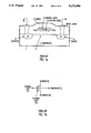
- FIG. 1a shows the physical structure of a conventional floating gate FET (n-channel).
- the floating gate FET includes a floating gate 2 which is electrically isolated from control gate 4 by a dielectric region 3, such as layered silicon dioxide. Both gates are electrically isolated from the underlying channel region 9 of the FET by the dielectric region.
- the channel region 9 is defined by identical n + -type source 6 and drain 8 regions formed in p-type substrate 7.
- the source 6 is connected to substrate 7 (usually grounded) and a positive potential is applied to the drain 8 via conductive metal layers connected to the source and drain regions through openings formed in the oxide layer 3.
- the equivalent circuit symbol is shown in FIG. 1b. It is to be understood, however, that source and drain regions are virtually interchangeable in a FET.
- Floating gate transistors are popular for use in memory devices, such as erasable-programmable-read-only-memory (EPROM), due to their ability to retain a charge across the floating gate 2 for long periods of time regardless of whether ordinary circuit voltages are applied to the circuit. This is true because a relatively large voltage (compared to circuit voltages) is required to overcome the oxide barrier and store or release a charge on the floating gate. The charge state is achieved by driving the drain junction to avalanche breakdown, so that high energy electrons will penetrate the thick oxide and become trapped on the floating gate. The charge is erased by shining ultraviolet light onto the device, thereby exciting the trapped electrons and causing them to move off the floating gate.
- EPROM erasable-programmable-read-only-memory
- V F which is required to store a charge on the floating gate
- V F V G *C 2 /(C 1 +C 2 )],
- C 1 the effective capacitance between the floating gate and the channel
- V G the voltage at the control gate.
- the floating gate voltage V F may be adjusted during fabrication of the device by using conventional diffusion or ion implantation techniques to adjust the dopant levels in the channel. Alternatively, the ratio of effective capacitances may be adjusted by varying the oxide thickness.
- a floating gate transistor may thus be used in a novel way, without regard to the charge-injection model just described, to protect against ESD, as will be hereinafter discussed.
- An MOS integrated circuit has circuit features whose proper operation is destroyed by the application of a voltage (ESD stress) exceeding a predetermined level.
- the circuit features are protected against ESD stress by switching means adapted to switch at a voltage level which is greater than the normal operating voltage of the integrated circuit but less than the predetermined voltage level of the circuit feature, thus shunting excess voltage away from the circuit feature.
- the switching means utilizes a floating gate transistor construction having a floating gate voltage which is greater than the normal operating voltage of the integrated circuit but slightly less than the predetermined voltage level of the circuit feature.
- a first floating gate transistor provides a path for a positive ESD stress by having its control gate and drain connected to the line of interest and its source connected to a reference point.
- a second floating gate transistor provides a path for a negative ESD stress by having its control gate and drain connected to the reference point and its source connected to the line of interest.
- the source potential is sufficiently below the control gate potential to turn the transistor on and induce the channel to conduct, thus shunting the ESD stress to the reference point and away from the line of interest.
- the present invention provides a simple method for diverting ESD stress. By fabricating a floating gate device to switch at a voltage level which is slightly less than the point where proper operation of an MOS device is destroyed, the integrity of the MOS device is protected.
- FIG. 1a is a side plan view of a conventional EPROM structure.
- FIG. 1b is a circuit diagram equivalent of the structure of FIG. 1.
- FIG. 2 is a circuit diagram of one aspect of the ESD protection circuit according to the present invention.
- FIG. 3 is a circuit diagram of a second embodiment of the ESD protection circuit according to the present invention.
- FIG. 4 is a circuit diagram of an alternative embodiment of the second aspect of the ESD protection circuit according to the present invention.
- FIG. 5 is a circuit diagram of a third aspect of the ESD protection circuit according to the present invention.
- FIG. 6 is a circuit diagram of the preferred embodiment of an ESD protection circuit according to the present invention.
- a conventional IC chip package electrical connections to the circuit are made via bonding pads on the surface of the IC structure.
- the bonding pads are accessible to the user via pins which extend from the IC chip package.
- the IC package will be plugged into a socket on a printed circuit board.
- floating gate transistors shunt the various circuit leads to a reference point (usually ground).
- the floating gate transistors are constructed according to conventional methods, such as those described above in the Background section. All floating gate transistors are designed to be off during normal IC operation.
- an IC package has a bonding pad 11 through which a user has access to the circuit feature which is connected to line 11a.
- a floating gate transistor 10 has its control gate 14 and drain 16 connected to line 11a and its source 18 connected to node 19.
- a second floating gate transistor 20 has its control gate 24 and its drain 26 connected to node 29 and its source 28 connected to line 11a.
- a user provides IC supply voltage V cc through pad 11.
- the user provides IC reference voltage V ss (usually ground) at nodes 19 and 29.
- the IC also has a bonding pad 12 where an output signal from the internal circuitry is presented.
- floating gate transistors 30, 40, 50 and 60 are connected along line 12a from pad 12 to protect the internal circuitry from ESD stress which may appear at pad 12.
- Transistor 30 has its control source 38 connected to V cc .
- Transistor 40 has its control gate 44 and drain 46 connected to V s and its source 48 connected to line 12a.
- Transistor 50 has its control gate 54 and drain 58 connected to V cc and its source 56 connected to line 12a.
- Transistor 60 has its control gate 64 and drain 68 connected to line 12a and its source 66 connected to reference voltage V ss .
- Transistors 70 and 80 are conventional FET buffer transistors of the type generally associated with output circuits.
- Transistor 70 is a p-channel FET with its drain 76 connected to line 12a, its source 78 connected to V cc and its gate 74 driven by the circuit.
- Transistor 80 is an n-channel FET with its source 86 tied to V ss , its drain 88 tied to line 12a and its gate 84 connected to the circuit.
- control gate 54 When a negative ESD stress (with respect to V cc ) appears at pad 12, control gate 54 is at a higher potential than source 56 and transistor 50 turns on, thus conducting the ESD stress from source 56 to drain 58 to line 11a, and not to the internal circuitry. Since the potential of control gate 34 is less than at source 38, transistor 30 remains off.
- the conventional buffer transistors 70 and 80 of FIG. 3 may be modified to take advantage of the floating gate principle in a simplified fabrication. Rather than having a true floating gate, transistors 70a and 80a use the circuit connection 72a to simulate a floating gate. Additionally, transistors 70a and 80a each have two control gates. Otherwise, the fabrication methods are conventional.
- Transistor 70a is a p-channel FET with its drain 76a connected to line 12a, source 78a connected to V cc , first gate 74a 1 tied to V cc , and second gate 74a 2 is tied to line 12a.
- Transistor 80a is a n-channel FET with its source 86a connected to V ss , drain 88a connected to line 12a, first gate 84a 1 tied to line 12a, and second gate 84a 2 is tied to V ss .
- the source and drain functions of transistors 70a and 80a are interchanged depending on which control gate is energized.
- drain 88a acts as a source by being dropped in potential below control gate 84a 2 enough to turn on transistor 80a, and the stress is conducted from source 88a to drain 86a to V ss .
- transistor 90 has two control gates 94a and 94b.
- Control gate 94a is connected to line 13a
- control gate 94b is connected to V cc
- source 96 is tied to line 13a
- drain 98 is tied to V cc .
- Transistor 100 has control gate 104a tied to line 13a, control gate 104b tied to V ss , source 106 connected to V ss , and drain 108 connected to line 13a.
- the source and drain functions of transistors 90 and 100 are interchanged depending on which control gate is energized.
- Buffer transistors 170 and 180 are conventional buffer transistors typically associated with input circuits.
- Transistor 170 is a p-channel FET with its drain 176 connected to the circuit, its source 178 connected to V cc , and its gate 174 tied to line 13a.
- Transistor 180 is an n-channel FET with its source 186 tied to V ss , its drain 188 connected to the circuit, and its gate 184 connected to line 13a.
- control gate 104a When a positive ESD stress (with respect to V ss ) appears at pad 13, control gate 104a is at a higher potential than source 106, and transistor 100 turns on, conducting the ESD stress from drain 108 to source 106 to V ss .
- control gate 94a When a positive ESD stress (with respect to V cc ) appears at pad 13, control gate 94a is at a higher potential than source 98 (interchanged), and transistor 90 turns on, conducting the ESD stress from drain 96 (interchanged) to source 98 to line 13a.
- control gate 94b When a negative ESD stress (with respect to V cc ) appears at pad 13, control gate 94b is at a higher potential than source 96, and transistor 90 turns on, conducting the ESD stress from source 96 to drain 98 to V cc .
- Transistors 10 and 20 are connected between V ss and V cc as described above with reference to FIG. 2.
- Line 11a is the V cc line.
- Transistors 30, 50 and 70 are connected between V cc and line 12a and transistors 40, 60, and 80 are connected between V ss and line 12a, as described above with reference to FIG. 3.
- Transistors 90 and 170 are connected between V ss and line 13a and transistors 100 and 180 are connected between V ss and line 13a, as described above with reference to FIG. 5. It is, of course, to be understood that typical chip packages have a plurality of other circuits which are accessible via bonding pads, each of which can be protected against ESD stress by the circuits and methods herein described.
- FIGS. 2, 3 and 5 above describe the primary conduction paths for each type of circuit. However, from FIG. 6, it is clear that there are interdependencies of the three types of circuits in a typical IC, such that alternative conduction paths are provided. It should also be clear that some of the transistors will be forward-biased under a particular set of conditions, providing a conduction path to the substrate. For example, a n-channel transistor will be forward biased by a negative ESD stress in a conventional manner. However, such conventional ESD protection methods are not discussed herein, since the present invention is directed to the use of floating gate transistor technology in a novel way, not as EPROM-type memory devices, but as shunts for ESD stress.
- control gate 54 When a positive ESD stress (with respect to V ss ) appears at pad 11, control gate 54 is at a higher potential than source 56 and transistor 50 turns on, conducting the stress from drain 58 to source 56 to line 12a. Control gate 64 is now at a higher potential than source 66 and transistor 60 turns on, conducting the ESD stress from drain 68 to source 66 to V ss .
- control gate 94b is at a higher potential than source 96 and transistor 90 turns on, conducting the stress from drain 98 to source 96 to line 13a.
- Control gate 104a is now at a higher potential than source 106 and transistor 100 turns on, conducting the ESD stress from drain 108 to source 106 to V ss .
- control gate 34 When a negative ESD stress (with respect to V ss ) appears at pad 11, control gate 34 is placed at a higher potential than source 38 and transistor 30 turns on. The ESD stress is thus conducted from source 38 to drain 36 to line 12a. Control gate 44 is now at a higher potential than source 48, and transistor 40 is turned on. Therefore, the ESD stress is conducted from source 48 to drain 46 to V ss .
- control gate 94a is at a higher potential than source 98, and transistor 90 turns on.
- the ESD stress is thus conducted from source 98 to drain 96 to line 13a.
- the potential at source 108 is now dropped sufficiently below that of control gate 104b to turn on transistor 100 on. Therefore, the ESD stress is conducted from source 108 to drain 106 to V ss .
- control gate 34 When a positive ESD stress appears (with respect to V ss ) appears at pad 12, control gate 34 is at a higher potential than source 38 and transistor 30 turns on, conducting the ESD stress from drain 36 to source 38 to line 11a. There, the potential presented at control gate 14 is still sufficient to turn on transistor 10, conducting the ESD stress from drain 16 to source 18 to V ss .
- drain 76 of p-channel transistor 70 is forward biased.
- the ESD stress is conducted from source 76 to drain 78 to line 11a, and then through transistor 10 to V ss as just described.
- control gate 64 When a positive ESD stress (with regard to V cc ) appears at pad 12, control gate 64 is at a higher potential than source 66, and transistor 60 turns on, conducting the ESD stress to V ss . Since source 26 and control gate 24 are connected to V ss , the potential from control gate 24 to drain 28 is sufficient to turn on transistor 20, and the ESD stress is conducted from drain 26 to source 28 to line 11a, the V cc line.
Landscapes
- Engineering & Computer Science (AREA)
- Microelectronics & Electronic Packaging (AREA)
- Semiconductor Integrated Circuits (AREA)
- Metal-Oxide And Bipolar Metal-Oxide Semiconductor Integrated Circuits (AREA)
- Insulated Gate Type Field-Effect Transistor (AREA)
Priority Applications (4)
| Application Number | Priority Date | Filing Date | Title |
|---|---|---|---|
| US07/647,740 US5272586A (en) | 1991-01-29 | 1991-01-29 | Technique for improving ESD immunity |
| EP19920300379 EP0497471A3 (en) | 1991-01-29 | 1992-01-16 | A technique for improving esd immunity |
| KR1019920001174A KR920015584A (ko) | 1991-01-29 | 1992-01-28 | Esd 면역성을 개선시키는 기술 |
| JP4013377A JPH06120494A (ja) | 1991-01-29 | 1992-01-28 | Esd免疫性改善技術 |
Applications Claiming Priority (1)
| Application Number | Priority Date | Filing Date | Title |
|---|---|---|---|
| US07/647,740 US5272586A (en) | 1991-01-29 | 1991-01-29 | Technique for improving ESD immunity |
Publications (1)
| Publication Number | Publication Date |
|---|---|
| US5272586A true US5272586A (en) | 1993-12-21 |
Family
ID=24598082
Family Applications (1)
| Application Number | Title | Priority Date | Filing Date |
|---|---|---|---|
| US07/647,740 Expired - Lifetime US5272586A (en) | 1991-01-29 | 1991-01-29 | Technique for improving ESD immunity |
Country Status (4)
| Country | Link |
|---|---|
| US (1) | US5272586A (de) |
| EP (1) | EP0497471A3 (de) |
| JP (1) | JPH06120494A (de) |
| KR (1) | KR920015584A (de) |
Cited By (26)
| Publication number | Priority date | Publication date | Assignee | Title |
|---|---|---|---|---|
| US5510728A (en) * | 1994-07-14 | 1996-04-23 | Vlsi Technology, Inc. | Multi-finger input buffer with transistor gates capacitively coupled to ground |
| US5696397A (en) * | 1995-04-28 | 1997-12-09 | Nec Corporation | Input protection circuit and method of fabricating semiconductor integrated circuit |
| US5729420A (en) * | 1995-12-20 | 1998-03-17 | Samsung Electronics Co., Ltd. | High voltage recoverable input protection circuit and protection device |
| US5745323A (en) * | 1995-06-30 | 1998-04-28 | Analog Devices, Inc. | Electrostatic discharge protection circuit for protecting CMOS transistors on integrated circuit processes |
| US5751525A (en) * | 1996-01-05 | 1998-05-12 | Analog Devices, Inc. | EOS/ESD Protection circuit for an integrated circuit with operating/test voltages exceeding power supply rail voltages |
| US5751051A (en) * | 1995-07-18 | 1998-05-12 | Nec Corporation | Semiconductor device equipped with electrostatic breakdown protection circuit |
| US5821797A (en) * | 1995-03-31 | 1998-10-13 | Kabushiki Kaisha Toshiba | Protection circuit for semiconductor devices |
| US5838146A (en) * | 1996-11-12 | 1998-11-17 | Analog Devices, Inc. | Method and apparatus for providing ESD/EOS protection for IC power supply pins |
| US5895959A (en) * | 1996-10-14 | 1999-04-20 | Vanguard International Semiconductor Corporation | Input port electrostatic discharge protection circuit for an intergrated circuit |
| US5917689A (en) * | 1996-09-12 | 1999-06-29 | Analog Devices, Inc. | General purpose EOS/ESD protection circuit for bipolar-CMOS and CMOS integrated circuits |
| US5963409A (en) * | 1996-10-14 | 1999-10-05 | Vanguard International Semiconductor Corporation | Input/output electrostatic discharge protection circuit for an integrated circuit (IC) |
| US5977594A (en) * | 1997-06-09 | 1999-11-02 | Nec Corporation | Protecting circuit for a semiconductor circuit |
| US6008508A (en) * | 1996-09-12 | 1999-12-28 | National Semiconductor Corporation | ESD Input protection using a floating gate neuron MOSFET as a tunable trigger element |
| US6163446A (en) * | 1997-09-02 | 2000-12-19 | Telefonaktiebolaget Lm Ericsson | Protective circuit |
| US20010050835A1 (en) * | 2000-06-07 | 2001-12-13 | Hiroyuki Uchida | Surge protection circuit for semiconductor devices |
| US6366435B1 (en) * | 2000-02-04 | 2002-04-02 | United Microelectronics Corp. | Multiple sources ESD protection for an epitaxy wafer substrate |
| CN1130020C (zh) * | 1997-07-28 | 2003-12-03 | 恩益禧电子股份有限公司 | 静电保护电路 |
| US6670679B2 (en) * | 2001-06-25 | 2003-12-30 | Nec Electronics Corporation | Semiconductor device having an ESD protective circuit |
| US6842318B2 (en) | 2001-03-15 | 2005-01-11 | Microsemi Corporation | Low leakage input protection device and scheme for electrostatic discharge |
| CN100403536C (zh) * | 2004-04-01 | 2008-07-16 | 凌阳科技股份有限公司 | 可承受高电压及负电压的静电放电保护装置 |
| KR100937652B1 (ko) | 2002-12-31 | 2010-01-19 | 동부일렉트로닉스 주식회사 | 반도체 장치의 정전기방전 보호회로 |
| US9577639B1 (en) * | 2015-09-24 | 2017-02-21 | Qualcomm Incorporated | Source separated cell |
| US20170117705A1 (en) * | 2015-10-23 | 2017-04-27 | Nlt Technologies, Ltd. | Protection circuit and electronic device |
| US10593709B2 (en) * | 2017-10-10 | 2020-03-17 | Innolux Corporation | Panel device and electronic device |
| US11158628B2 (en) * | 2019-09-29 | 2021-10-26 | Xiamen Tianma Micro-Electronics Co., Ltd. | Electro-static discharge circuit, array substrate, display panel and display apparatus |
| US11468812B2 (en) * | 2020-08-25 | 2022-10-11 | Lg Display Co., Ltd. | Display apparatus |
Families Citing this family (9)
| Publication number | Priority date | Publication date | Assignee | Title |
|---|---|---|---|---|
| US5276582A (en) * | 1992-08-12 | 1994-01-04 | National Semiconductor Corporation | ESD protection using npn bipolar transistor |
| US5572394A (en) * | 1995-04-06 | 1996-11-05 | Industrial Technology Research Institute | CMOS on-chip four-LVTSCR ESD protection scheme |
| US5754380A (en) * | 1995-04-06 | 1998-05-19 | Industrial Technology Research Institute | CMOS output buffer with enhanced high ESD protection capability |
| JPH09148452A (ja) * | 1995-11-09 | 1997-06-06 | Ind Technol Res Inst | 静電放電防護能力を強化したcmos出力バッファ |
| JP3400215B2 (ja) * | 1995-11-21 | 2003-04-28 | 沖電気工業株式会社 | 半導体装置 |
| DE29812092U1 (de) | 1998-07-07 | 1999-11-18 | iC-Haus GmbH, 55294 Bodenheim | Elektronischer Wechselspannungsschalter |
| KR100443510B1 (ko) * | 2001-12-22 | 2004-08-09 | 주식회사 하이닉스반도체 | 정전기 보호 회로 |
| KR100861193B1 (ko) * | 2002-07-18 | 2008-09-30 | 주식회사 하이닉스반도체 | 정전기 방전 보호 회로 |
| JP5041672B2 (ja) * | 2004-04-09 | 2012-10-03 | 株式会社半導体エネルギー研究所 | 半導体装置 |
Citations (11)
| Publication number | Priority date | Publication date | Assignee | Title |
|---|---|---|---|---|
| EP0055552A2 (de) * | 1980-12-26 | 1982-07-07 | Fujitsu Limited | Eingangsschutzschaltung für einen MIS-Transistor |
| US4527213A (en) * | 1981-11-27 | 1985-07-02 | Tokyo Shibaura Denki Kabushiki Kaisha | Semiconductor integrated circuit device with circuits for protecting an input section against an external surge |
| EP0169559A2 (de) * | 1984-07-24 | 1986-01-29 | Nec Corporation | Halbleitervorrichtung mit Eingangs-/Ausgangsschutzschaltung |
| US4630162A (en) * | 1984-07-31 | 1986-12-16 | Texas Instruments Incorporated | ESD input protection circuit |
| WO1987002511A1 (en) * | 1985-10-15 | 1987-04-23 | American Telephone & Telegraph Company | Protection of igfet integrated circuits from electrostatic discharge |
| US4692834A (en) * | 1984-08-20 | 1987-09-08 | Kabushiki Kaisha Toshiba | Electrostatic discharge protection circuit with variable limiting threshold for MOS device |
| EP0257774A1 (de) * | 1986-07-24 | 1988-03-02 | Fujitsu Limited | Schutzschaltung für hochintegrierte Schaltung |
| EP0291242A2 (de) * | 1987-05-15 | 1988-11-17 | Advanced Micro Devices, Inc. | Schutzsystem für CMOS-integrierte Schaltungen |
| US4890187A (en) * | 1987-11-06 | 1989-12-26 | Sgs-Thomson Microelectronics, Sa | Integrated circuit protected against electrostatic discharges, with variable protection threshold |
| US4896243A (en) * | 1988-12-20 | 1990-01-23 | Texas Instruments Incorporated | Efficient ESD input protection scheme |
| US5111262A (en) * | 1988-08-10 | 1992-05-05 | Actel Corporation | Structure for protecting thin dielectrics during processing |
-
1991
- 1991-01-29 US US07/647,740 patent/US5272586A/en not_active Expired - Lifetime
-
1992
- 1992-01-16 EP EP19920300379 patent/EP0497471A3/en not_active Withdrawn
- 1992-01-28 JP JP4013377A patent/JPH06120494A/ja active Pending
- 1992-01-28 KR KR1019920001174A patent/KR920015584A/ko not_active Application Discontinuation
Patent Citations (14)
| Publication number | Priority date | Publication date | Assignee | Title |
|---|---|---|---|---|
| EP0055552A2 (de) * | 1980-12-26 | 1982-07-07 | Fujitsu Limited | Eingangsschutzschaltung für einen MIS-Transistor |
| US4449158A (en) * | 1980-12-26 | 1984-05-15 | Fujitsu Limited | Input protection circuit for MIS transistor |
| US4527213A (en) * | 1981-11-27 | 1985-07-02 | Tokyo Shibaura Denki Kabushiki Kaisha | Semiconductor integrated circuit device with circuits for protecting an input section against an external surge |
| EP0169559A2 (de) * | 1984-07-24 | 1986-01-29 | Nec Corporation | Halbleitervorrichtung mit Eingangs-/Ausgangsschutzschaltung |
| US4630162A (en) * | 1984-07-31 | 1986-12-16 | Texas Instruments Incorporated | ESD input protection circuit |
| US4692834A (en) * | 1984-08-20 | 1987-09-08 | Kabushiki Kaisha Toshiba | Electrostatic discharge protection circuit with variable limiting threshold for MOS device |
| US4692834B1 (de) * | 1984-08-20 | 1993-03-02 | Tokyo Shibaura Electric Co | |
| WO1987002511A1 (en) * | 1985-10-15 | 1987-04-23 | American Telephone & Telegraph Company | Protection of igfet integrated circuits from electrostatic discharge |
| EP0257774A1 (de) * | 1986-07-24 | 1988-03-02 | Fujitsu Limited | Schutzschaltung für hochintegrierte Schaltung |
| EP0291242A2 (de) * | 1987-05-15 | 1988-11-17 | Advanced Micro Devices, Inc. | Schutzsystem für CMOS-integrierte Schaltungen |
| US4819047A (en) * | 1987-05-15 | 1989-04-04 | Advanced Micro Devices, Inc. | Protection system for CMOS integrated circuits |
| US4890187A (en) * | 1987-11-06 | 1989-12-26 | Sgs-Thomson Microelectronics, Sa | Integrated circuit protected against electrostatic discharges, with variable protection threshold |
| US5111262A (en) * | 1988-08-10 | 1992-05-05 | Actel Corporation | Structure for protecting thin dielectrics during processing |
| US4896243A (en) * | 1988-12-20 | 1990-01-23 | Texas Instruments Incorporated | Efficient ESD input protection scheme |
Cited By (28)
| Publication number | Priority date | Publication date | Assignee | Title |
|---|---|---|---|---|
| US5510728A (en) * | 1994-07-14 | 1996-04-23 | Vlsi Technology, Inc. | Multi-finger input buffer with transistor gates capacitively coupled to ground |
| US5821797A (en) * | 1995-03-31 | 1998-10-13 | Kabushiki Kaisha Toshiba | Protection circuit for semiconductor devices |
| US5696397A (en) * | 1995-04-28 | 1997-12-09 | Nec Corporation | Input protection circuit and method of fabricating semiconductor integrated circuit |
| US5745323A (en) * | 1995-06-30 | 1998-04-28 | Analog Devices, Inc. | Electrostatic discharge protection circuit for protecting CMOS transistors on integrated circuit processes |
| US5751051A (en) * | 1995-07-18 | 1998-05-12 | Nec Corporation | Semiconductor device equipped with electrostatic breakdown protection circuit |
| US5729420A (en) * | 1995-12-20 | 1998-03-17 | Samsung Electronics Co., Ltd. | High voltage recoverable input protection circuit and protection device |
| US5751525A (en) * | 1996-01-05 | 1998-05-12 | Analog Devices, Inc. | EOS/ESD Protection circuit for an integrated circuit with operating/test voltages exceeding power supply rail voltages |
| US6008508A (en) * | 1996-09-12 | 1999-12-28 | National Semiconductor Corporation | ESD Input protection using a floating gate neuron MOSFET as a tunable trigger element |
| US5917689A (en) * | 1996-09-12 | 1999-06-29 | Analog Devices, Inc. | General purpose EOS/ESD protection circuit for bipolar-CMOS and CMOS integrated circuits |
| US5895959A (en) * | 1996-10-14 | 1999-04-20 | Vanguard International Semiconductor Corporation | Input port electrostatic discharge protection circuit for an intergrated circuit |
| US5963409A (en) * | 1996-10-14 | 1999-10-05 | Vanguard International Semiconductor Corporation | Input/output electrostatic discharge protection circuit for an integrated circuit (IC) |
| US5838146A (en) * | 1996-11-12 | 1998-11-17 | Analog Devices, Inc. | Method and apparatus for providing ESD/EOS protection for IC power supply pins |
| US5977594A (en) * | 1997-06-09 | 1999-11-02 | Nec Corporation | Protecting circuit for a semiconductor circuit |
| CN1130020C (zh) * | 1997-07-28 | 2003-12-03 | 恩益禧电子股份有限公司 | 静电保护电路 |
| US6163446A (en) * | 1997-09-02 | 2000-12-19 | Telefonaktiebolaget Lm Ericsson | Protective circuit |
| US6366435B1 (en) * | 2000-02-04 | 2002-04-02 | United Microelectronics Corp. | Multiple sources ESD protection for an epitaxy wafer substrate |
| US20010050835A1 (en) * | 2000-06-07 | 2001-12-13 | Hiroyuki Uchida | Surge protection circuit for semiconductor devices |
| US6812528B2 (en) * | 2000-06-07 | 2004-11-02 | Nec Corporation | Surge protection circuit for semiconductor devices |
| US6842318B2 (en) | 2001-03-15 | 2005-01-11 | Microsemi Corporation | Low leakage input protection device and scheme for electrostatic discharge |
| US6670679B2 (en) * | 2001-06-25 | 2003-12-30 | Nec Electronics Corporation | Semiconductor device having an ESD protective circuit |
| KR100937652B1 (ko) | 2002-12-31 | 2010-01-19 | 동부일렉트로닉스 주식회사 | 반도체 장치의 정전기방전 보호회로 |
| CN100403536C (zh) * | 2004-04-01 | 2008-07-16 | 凌阳科技股份有限公司 | 可承受高电压及负电压的静电放电保护装置 |
| US9577639B1 (en) * | 2015-09-24 | 2017-02-21 | Qualcomm Incorporated | Source separated cell |
| US20170117705A1 (en) * | 2015-10-23 | 2017-04-27 | Nlt Technologies, Ltd. | Protection circuit and electronic device |
| US10291021B2 (en) * | 2015-10-23 | 2019-05-14 | Nlt Technologies, Ltd. | Protection circuit and electronic device |
| US10593709B2 (en) * | 2017-10-10 | 2020-03-17 | Innolux Corporation | Panel device and electronic device |
| US11158628B2 (en) * | 2019-09-29 | 2021-10-26 | Xiamen Tianma Micro-Electronics Co., Ltd. | Electro-static discharge circuit, array substrate, display panel and display apparatus |
| US11468812B2 (en) * | 2020-08-25 | 2022-10-11 | Lg Display Co., Ltd. | Display apparatus |
Also Published As
| Publication number | Publication date |
|---|---|
| EP0497471A3 (en) | 1993-05-19 |
| JPH06120494A (ja) | 1994-04-28 |
| EP0497471A2 (de) | 1992-08-05 |
| KR920015584A (ko) | 1992-08-27 |
Similar Documents
| Publication | Publication Date | Title |
|---|---|---|
| US5272586A (en) | Technique for improving ESD immunity | |
| US5237395A (en) | Power rail ESD protection circuit | |
| KR100260960B1 (ko) | 상보형 금속 산화물 반도체 집적 회로용 정전방전보호 | |
| JP3275095B2 (ja) | 集積回路の過渡防護開路 | |
| US5617283A (en) | Self-referencing modulation circuit for CMOS integrated circuit electrostatic discharge protection clamps | |
| US6008684A (en) | CMOS output buffer with CMOS-controlled lateral SCR devices | |
| US5959488A (en) | Dual-node capacitor coupled MOSFET for improving ESD performance | |
| US5946175A (en) | Secondary ESD/EOS protection circuit | |
| US7274546B2 (en) | Apparatus and method for improved triggering and leakage current control of ESD clamping devices | |
| JP3926975B2 (ja) | スタック型mosトランジスタ保護回路 | |
| US4876584A (en) | Electrostatic discharge protection circuit | |
| CA1282186C (en) | Mos i/o protection using switched body circuit design | |
| KR101006827B1 (ko) | 저 전압 nmos-기반 정전기 방전 클램프 | |
| EP0740859B1 (de) | Elektrostatische entladungsschaltung für eine hochspannungsschaltung mit hoher geschwindigkeit | |
| CN1829411B (zh) | 静电放电电路 | |
| US6624998B2 (en) | Electrostatic discharge protection scheme in low potential drop environments | |
| JP2878587B2 (ja) | 半導体装置 | |
| US5729419A (en) | Changed device model electrostatic discharge protection circuit for output drivers and method of implementing same | |
| US5535086A (en) | ESD protection circuit and method for BICMOS devices | |
| US5910873A (en) | Field oxide transistor based feedback circuit for electrical overstress protection | |
| KR100772693B1 (ko) | 반도체 장치의 정전기 보호회로 | |
| US5644459A (en) | Bipolarity electrostatic discharge protection device and method for making same | |
| KR100587089B1 (ko) | 반도체 장치용 정전기 보호장치 | |
| KR100504203B1 (ko) | 반도체장치의 보호소자 | |
| KR100200303B1 (ko) | 반도체 장치용 정전기 방지회로 및 그 제조방법 |
Legal Events
| Date | Code | Title | Description |
|---|---|---|---|
| AS | Assignment |
Owner name: NATIONAL SEMICONDUCTOR CORPORATION, A CORP. OF DE Free format text: ASSIGNMENT OF ASSIGNORS INTEREST.;ASSIGNOR:YEN, YUNG-CHAU;REEL/FRAME:005595/0264 Effective date: 19910124 Owner name: NATIONAL SEMICONDUCTOR CORPORATION, A CORP. OF DE, Free format text: ASSIGNMENT OF ASSIGNORS INTEREST;ASSIGNOR:YEN, YUNG-CHAU;REEL/FRAME:005595/0264 Effective date: 19910124 |
|
| STCF | Information on status: patent grant |
Free format text: PATENTED CASE |
|
| FPAY | Fee payment |
Year of fee payment: 4 |
|
| FPAY | Fee payment |
Year of fee payment: 8 |
|
| REMI | Maintenance fee reminder mailed | ||
| FPAY | Fee payment |
Year of fee payment: 12 |