JP5041672B2 - 半導体装置 - Google Patents
半導体装置 Download PDFInfo
- Publication number
- JP5041672B2 JP5041672B2 JP2005111799A JP2005111799A JP5041672B2 JP 5041672 B2 JP5041672 B2 JP 5041672B2 JP 2005111799 A JP2005111799 A JP 2005111799A JP 2005111799 A JP2005111799 A JP 2005111799A JP 5041672 B2 JP5041672 B2 JP 5041672B2
- Authority
- JP
- Japan
- Prior art keywords
- transistor
- voltage
- drain
- gate
- antenna
- Prior art date
- Legal status (The legal status is an assumption and is not a legal conclusion. Google has not performed a legal analysis and makes no representation as to the accuracy of the status listed.)
- Expired - Fee Related
Links
- 239000004065 semiconductor Substances 0.000 title claims description 186
- 239000010408 film Substances 0.000 claims description 317
- 238000007667 floating Methods 0.000 claims description 56
- 239000010409 thin film Substances 0.000 claims description 3
- 239000000758 substrate Substances 0.000 description 114
- 238000000034 method Methods 0.000 description 77
- 239000011229 interlayer Substances 0.000 description 54
- 239000000463 material Substances 0.000 description 48
- 239000000853 adhesive Substances 0.000 description 36
- 230000001070 adhesive effect Effects 0.000 description 36
- 239000007789 gas Substances 0.000 description 34
- 239000010410 layer Substances 0.000 description 30
- 238000004519 manufacturing process Methods 0.000 description 28
- 239000011347 resin Substances 0.000 description 27
- 229920005989 resin Polymers 0.000 description 27
- 238000005530 etching Methods 0.000 description 26
- 238000010586 diagram Methods 0.000 description 24
- 239000011521 glass Substances 0.000 description 23
- 229910052581 Si3N4 Inorganic materials 0.000 description 22
- XUIMIQQOPSSXEZ-UHFFFAOYSA-N Silicon Chemical compound [Si] XUIMIQQOPSSXEZ-UHFFFAOYSA-N 0.000 description 22
- 229910052710 silicon Inorganic materials 0.000 description 22
- 239000010703 silicon Substances 0.000 description 22
- VYPSYNLAJGMNEJ-UHFFFAOYSA-N silicon dioxide Inorganic materials O=[Si]=O VYPSYNLAJGMNEJ-UHFFFAOYSA-N 0.000 description 22
- HQVNEWCFYHHQES-UHFFFAOYSA-N silicon nitride Chemical compound N12[Si]34N5[Si]62N3[Si]51N64 HQVNEWCFYHHQES-UHFFFAOYSA-N 0.000 description 22
- 229910052814 silicon oxide Inorganic materials 0.000 description 20
- 239000012535 impurity Substances 0.000 description 18
- 239000002585 base Substances 0.000 description 17
- UFHFLCQGNIYNRP-UHFFFAOYSA-N Hydrogen Chemical compound [H][H] UFHFLCQGNIYNRP-UHFFFAOYSA-N 0.000 description 15
- 239000001257 hydrogen Substances 0.000 description 15
- 229910052739 hydrogen Inorganic materials 0.000 description 15
- 230000006870 function Effects 0.000 description 13
- 229910052751 metal Inorganic materials 0.000 description 13
- 239000002184 metal Substances 0.000 description 13
- 230000001965 increasing effect Effects 0.000 description 12
- 230000002829 reductive effect Effects 0.000 description 12
- 239000013078 crystal Substances 0.000 description 11
- 230000000670 limiting effect Effects 0.000 description 11
- 150000002736 metal compounds Chemical class 0.000 description 11
- 238000012937 correction Methods 0.000 description 10
- KPUWHANPEXNPJT-UHFFFAOYSA-N disiloxane Chemical class [SiH3]O[SiH3] KPUWHANPEXNPJT-UHFFFAOYSA-N 0.000 description 10
- 238000005268 plasma chemical vapour deposition Methods 0.000 description 10
- 230000008569 process Effects 0.000 description 10
- -1 halogen fluoride Chemical class 0.000 description 9
- 238000010438 heat treatment Methods 0.000 description 8
- 230000015654 memory Effects 0.000 description 8
- 238000007639 printing Methods 0.000 description 8
- 238000000926 separation method Methods 0.000 description 8
- 229910021332 silicide Inorganic materials 0.000 description 8
- FVBUAEGBCNSCDD-UHFFFAOYSA-N silicide(4-) Chemical compound [Si-4] FVBUAEGBCNSCDD-UHFFFAOYSA-N 0.000 description 8
- 238000002425 crystallisation Methods 0.000 description 7
- 238000005499 laser crystallization Methods 0.000 description 7
- 238000000059 patterning Methods 0.000 description 7
- 239000011241 protective layer Substances 0.000 description 7
- 230000008901 benefit Effects 0.000 description 6
- 239000004020 conductor Substances 0.000 description 6
- 239000002784 hot electron Substances 0.000 description 6
- 238000002347 injection Methods 0.000 description 6
- 239000007924 injection Substances 0.000 description 6
- 229920003023 plastic Polymers 0.000 description 6
- 239000004033 plastic Substances 0.000 description 6
- 125000001424 substituent group Chemical group 0.000 description 6
- 229910052715 tantalum Inorganic materials 0.000 description 6
- MZLGASXMSKOWSE-UHFFFAOYSA-N tantalum nitride Chemical compound [Ta]#N MZLGASXMSKOWSE-UHFFFAOYSA-N 0.000 description 6
- 239000010936 titanium Substances 0.000 description 6
- 239000004642 Polyimide Substances 0.000 description 5
- 230000015556 catabolic process Effects 0.000 description 5
- 239000000460 chlorine Substances 0.000 description 5
- 230000000694 effects Effects 0.000 description 5
- 229910052736 halogen Inorganic materials 0.000 description 5
- 230000010355 oscillation Effects 0.000 description 5
- 239000005022 packaging material Substances 0.000 description 5
- 229920001721 polyimide Polymers 0.000 description 5
- 238000004544 sputter deposition Methods 0.000 description 5
- GUVRBAGPIYLISA-UHFFFAOYSA-N tantalum atom Chemical compound [Ta] GUVRBAGPIYLISA-UHFFFAOYSA-N 0.000 description 5
- XKRFYHLGVUSROY-UHFFFAOYSA-N Argon Chemical compound [Ar] XKRFYHLGVUSROY-UHFFFAOYSA-N 0.000 description 4
- IJGRMHOSHXDMSA-UHFFFAOYSA-N Atomic nitrogen Chemical compound N#N IJGRMHOSHXDMSA-UHFFFAOYSA-N 0.000 description 4
- KRHYYFGTRYWZRS-UHFFFAOYSA-N Fluorane Chemical compound F KRHYYFGTRYWZRS-UHFFFAOYSA-N 0.000 description 4
- 229910052783 alkali metal Inorganic materials 0.000 description 4
- 150000001340 alkali metals Chemical class 0.000 description 4
- 229910052784 alkaline earth metal Inorganic materials 0.000 description 4
- 150000001342 alkaline earth metals Chemical class 0.000 description 4
- 229910021417 amorphous silicon Inorganic materials 0.000 description 4
- 230000003197 catalytic effect Effects 0.000 description 4
- 238000004891 communication Methods 0.000 description 4
- 125000001153 fluoro group Chemical group F* 0.000 description 4
- 238000005984 hydrogenation reaction Methods 0.000 description 4
- 229910052759 nickel Inorganic materials 0.000 description 4
- PXHVJJICTQNCMI-UHFFFAOYSA-N nickel Substances [Ni] PXHVJJICTQNCMI-UHFFFAOYSA-N 0.000 description 4
- 125000000962 organic group Chemical group 0.000 description 4
- 238000002161 passivation Methods 0.000 description 4
- 238000000206 photolithography Methods 0.000 description 4
- 229910052718 tin Inorganic materials 0.000 description 4
- 229910052719 titanium Inorganic materials 0.000 description 4
- OKTJSMMVPCPJKN-UHFFFAOYSA-N Carbon Chemical compound [C] OKTJSMMVPCPJKN-UHFFFAOYSA-N 0.000 description 3
- 239000004593 Epoxy Substances 0.000 description 3
- 239000004952 Polyamide Substances 0.000 description 3
- ATJFFYVFTNAWJD-UHFFFAOYSA-N Tin Chemical compound [Sn] ATJFFYVFTNAWJD-UHFFFAOYSA-N 0.000 description 3
- 230000001133 acceleration Effects 0.000 description 3
- NIXOWILDQLNWCW-UHFFFAOYSA-N acrylic acid group Chemical group C(C=C)(=O)O NIXOWILDQLNWCW-UHFFFAOYSA-N 0.000 description 3
- 238000004380 ashing Methods 0.000 description 3
- 229910052799 carbon Inorganic materials 0.000 description 3
- 229910052802 copper Inorganic materials 0.000 description 3
- 230000007547 defect Effects 0.000 description 3
- 230000002950 deficient Effects 0.000 description 3
- 238000009826 distribution Methods 0.000 description 3
- 230000005674 electromagnetic induction Effects 0.000 description 3
- 229910052737 gold Inorganic materials 0.000 description 3
- 239000001307 helium Substances 0.000 description 3
- 229910052734 helium Inorganic materials 0.000 description 3
- SWQJXJOGLNCZEY-UHFFFAOYSA-N helium atom Chemical compound [He] SWQJXJOGLNCZEY-UHFFFAOYSA-N 0.000 description 3
- 230000001678 irradiating effect Effects 0.000 description 3
- 229910044991 metal oxide Inorganic materials 0.000 description 3
- 150000004706 metal oxides Chemical class 0.000 description 3
- 229910052698 phosphorus Inorganic materials 0.000 description 3
- 229920002647 polyamide Polymers 0.000 description 3
- 239000002356 single layer Substances 0.000 description 3
- 238000004528 spin coating Methods 0.000 description 3
- 229920001187 thermosetting polymer Polymers 0.000 description 3
- 229910052721 tungsten Inorganic materials 0.000 description 3
- 229920000178 Acrylic resin Polymers 0.000 description 2
- 239000004925 Acrylic resin Substances 0.000 description 2
- 229910018125 Al-Si Inorganic materials 0.000 description 2
- 229910018520 Al—Si Inorganic materials 0.000 description 2
- OAICVXFJPJFONN-UHFFFAOYSA-N Phosphorus Chemical compound [P] OAICVXFJPJFONN-UHFFFAOYSA-N 0.000 description 2
- 239000004696 Poly ether ether ketone Substances 0.000 description 2
- 239000004697 Polyetherimide Substances 0.000 description 2
- 239000004743 Polypropylene Substances 0.000 description 2
- 229910000577 Silicon-germanium Inorganic materials 0.000 description 2
- BOTDANWDWHJENH-UHFFFAOYSA-N Tetraethyl orthosilicate Chemical compound CCO[Si](OCC)(OCC)OCC BOTDANWDWHJENH-UHFFFAOYSA-N 0.000 description 2
- LEVVHYCKPQWKOP-UHFFFAOYSA-N [Si].[Ge] Chemical compound [Si].[Ge] LEVVHYCKPQWKOP-UHFFFAOYSA-N 0.000 description 2
- 230000002411 adverse Effects 0.000 description 2
- 125000000217 alkyl group Chemical group 0.000 description 2
- 239000005407 aluminoborosilicate glass Substances 0.000 description 2
- 238000000137 annealing Methods 0.000 description 2
- 229910052786 argon Inorganic materials 0.000 description 2
- 150000004945 aromatic hydrocarbons Chemical class 0.000 description 2
- 229910052785 arsenic Inorganic materials 0.000 description 2
- 239000012298 atmosphere Substances 0.000 description 2
- 125000004429 atom Chemical group 0.000 description 2
- 229910052788 barium Inorganic materials 0.000 description 2
- DSAJWYNOEDNPEQ-UHFFFAOYSA-N barium atom Chemical compound [Ba] DSAJWYNOEDNPEQ-UHFFFAOYSA-N 0.000 description 2
- 230000005540 biological transmission Effects 0.000 description 2
- 239000005388 borosilicate glass Substances 0.000 description 2
- 239000002775 capsule Substances 0.000 description 2
- 230000008859 change Effects 0.000 description 2
- 229910052804 chromium Inorganic materials 0.000 description 2
- 238000010168 coupling process Methods 0.000 description 2
- 238000000354 decomposition reaction Methods 0.000 description 2
- 239000000428 dust Substances 0.000 description 2
- 150000002367 halogens Chemical class 0.000 description 2
- 229910010272 inorganic material Inorganic materials 0.000 description 2
- 239000011147 inorganic material Substances 0.000 description 2
- 229910052742 iron Inorganic materials 0.000 description 2
- 229910052743 krypton Inorganic materials 0.000 description 2
- DNNSSWSSYDEUBZ-UHFFFAOYSA-N krypton atom Chemical compound [Kr] DNNSSWSSYDEUBZ-UHFFFAOYSA-N 0.000 description 2
- 239000007788 liquid Substances 0.000 description 2
- 229910052754 neon Inorganic materials 0.000 description 2
- GKAOGPIIYCISHV-UHFFFAOYSA-N neon atom Chemical compound [Ne] GKAOGPIIYCISHV-UHFFFAOYSA-N 0.000 description 2
- 229910052757 nitrogen Inorganic materials 0.000 description 2
- 239000012299 nitrogen atmosphere Substances 0.000 description 2
- 230000003287 optical effect Effects 0.000 description 2
- 239000011368 organic material Substances 0.000 description 2
- JMANVNJQNLATNU-UHFFFAOYSA-N oxalonitrile Chemical compound N#CC#N JMANVNJQNLATNU-UHFFFAOYSA-N 0.000 description 2
- 239000002245 particle Substances 0.000 description 2
- 239000011574 phosphorus Substances 0.000 description 2
- 229920002492 poly(sulfone) Polymers 0.000 description 2
- 229920001230 polyarylate Polymers 0.000 description 2
- 229920001707 polybutylene terephthalate Polymers 0.000 description 2
- 229920002530 polyetherether ketone Polymers 0.000 description 2
- 229920001601 polyetherimide Polymers 0.000 description 2
- 229920000139 polyethylene terephthalate Polymers 0.000 description 2
- 239000005020 polyethylene terephthalate Substances 0.000 description 2
- 229920001155 polypropylene Polymers 0.000 description 2
- 239000010453 quartz Substances 0.000 description 2
- 229910052709 silver Inorganic materials 0.000 description 2
- 239000002904 solvent Substances 0.000 description 2
- 238000002230 thermal chemical vapour deposition Methods 0.000 description 2
- WFKWXMTUELFFGS-UHFFFAOYSA-N tungsten Chemical compound [W] WFKWXMTUELFFGS-UHFFFAOYSA-N 0.000 description 2
- 239000010937 tungsten Substances 0.000 description 2
- 230000005641 tunneling Effects 0.000 description 2
- 238000001039 wet etching Methods 0.000 description 2
- 229910052725 zinc Inorganic materials 0.000 description 2
- NIXOWILDQLNWCW-UHFFFAOYSA-M Acrylate Chemical compound [O-]C(=O)C=C NIXOWILDQLNWCW-UHFFFAOYSA-M 0.000 description 1
- ZOXJGFHDIHLPTG-UHFFFAOYSA-N Boron Chemical compound [B] ZOXJGFHDIHLPTG-UHFFFAOYSA-N 0.000 description 1
- JOYRKODLDBILNP-UHFFFAOYSA-N Ethyl urethane Chemical compound CCOC(N)=O JOYRKODLDBILNP-UHFFFAOYSA-N 0.000 description 1
- 229910005883 NiSi Inorganic materials 0.000 description 1
- 239000004677 Nylon Substances 0.000 description 1
- 229920012266 Poly(ether sulfone) PES Polymers 0.000 description 1
- 239000004698 Polyethylene Substances 0.000 description 1
- 239000004793 Polystyrene Substances 0.000 description 1
- 238000001237 Raman spectrum Methods 0.000 description 1
- 229910003902 SiCl 4 Inorganic materials 0.000 description 1
- 229910004205 SiNX Inorganic materials 0.000 description 1
- 229910002808 Si–O–Si Inorganic materials 0.000 description 1
- GWEVSGVZZGPLCZ-UHFFFAOYSA-N Titan oxide Chemical compound O=[Ti]=O GWEVSGVZZGPLCZ-UHFFFAOYSA-N 0.000 description 1
- RTAQQCXQSZGOHL-UHFFFAOYSA-N Titanium Chemical compound [Ti] RTAQQCXQSZGOHL-UHFFFAOYSA-N 0.000 description 1
- 238000002441 X-ray diffraction Methods 0.000 description 1
- GDFCWFBWQUEQIJ-UHFFFAOYSA-N [B].[P] Chemical compound [B].[P] GDFCWFBWQUEQIJ-UHFFFAOYSA-N 0.000 description 1
- 238000009825 accumulation Methods 0.000 description 1
- XECAHXYUAAWDEL-UHFFFAOYSA-N acrylonitrile butadiene styrene Chemical compound C=CC=C.C=CC#N.C=CC1=CC=CC=C1 XECAHXYUAAWDEL-UHFFFAOYSA-N 0.000 description 1
- 239000004676 acrylonitrile butadiene styrene Substances 0.000 description 1
- 229920000122 acrylonitrile butadiene styrene Polymers 0.000 description 1
- 150000001298 alcohols Chemical class 0.000 description 1
- 229910052782 aluminium Inorganic materials 0.000 description 1
- PNEYBMLMFCGWSK-UHFFFAOYSA-N aluminium oxide Inorganic materials [O-2].[O-2].[O-2].[Al+3].[Al+3] PNEYBMLMFCGWSK-UHFFFAOYSA-N 0.000 description 1
- RQNWIZPPADIBDY-UHFFFAOYSA-N arsenic atom Chemical compound [As] RQNWIZPPADIBDY-UHFFFAOYSA-N 0.000 description 1
- 238000001505 atmospheric-pressure chemical vapour deposition Methods 0.000 description 1
- QVGXLLKOCUKJST-UHFFFAOYSA-N atomic oxygen Chemical compound [O] QVGXLLKOCUKJST-UHFFFAOYSA-N 0.000 description 1
- 230000002238 attenuated effect Effects 0.000 description 1
- 238000005452 bending Methods 0.000 description 1
- UMIVXZPTRXBADB-UHFFFAOYSA-N benzocyclobutene Chemical compound C1=CC=C2CCC2=C1 UMIVXZPTRXBADB-UHFFFAOYSA-N 0.000 description 1
- 230000033228 biological regulation Effects 0.000 description 1
- 229910052796 boron Inorganic materials 0.000 description 1
- 239000005380 borophosphosilicate glass Substances 0.000 description 1
- 239000000969 carrier Substances 0.000 description 1
- 239000000919 ceramic Substances 0.000 description 1
- 238000006243 chemical reaction Methods 0.000 description 1
- SLLGVCUQYRMELA-UHFFFAOYSA-N chlorosilicon Chemical compound Cl[Si] SLLGVCUQYRMELA-UHFFFAOYSA-N 0.000 description 1
- 238000004140 cleaning Methods 0.000 description 1
- 239000011248 coating agent Substances 0.000 description 1
- 238000000576 coating method Methods 0.000 description 1
- PMHQVHHXPFUNSP-UHFFFAOYSA-M copper(1+);methylsulfanylmethane;bromide Chemical compound Br[Cu].CSC PMHQVHHXPFUNSP-UHFFFAOYSA-M 0.000 description 1
- 238000005336 cracking Methods 0.000 description 1
- 230000008025 crystallization Effects 0.000 description 1
- 238000007865 diluting Methods 0.000 description 1
- 238000010790 dilution Methods 0.000 description 1
- 239000012895 dilution Substances 0.000 description 1
- 238000003618 dip coating Methods 0.000 description 1
- 238000001312 dry etching Methods 0.000 description 1
- 230000002708 enhancing effect Effects 0.000 description 1
- 238000001704 evaporation Methods 0.000 description 1
- 239000000945 filler Substances 0.000 description 1
- 238000011049 filling Methods 0.000 description 1
- 235000013305 food Nutrition 0.000 description 1
- SCCCLDWUZODEKG-UHFFFAOYSA-N germanide Chemical compound [GeH3-] SCCCLDWUZODEKG-UHFFFAOYSA-N 0.000 description 1
- 229910052732 germanium Inorganic materials 0.000 description 1
- GNPVGFCGXDBREM-UHFFFAOYSA-N germanium atom Chemical compound [Ge] GNPVGFCGXDBREM-UHFFFAOYSA-N 0.000 description 1
- 239000010931 gold Substances 0.000 description 1
- 239000011261 inert gas Substances 0.000 description 1
- 238000009413 insulation Methods 0.000 description 1
- 238000010030 laminating Methods 0.000 description 1
- 238000004518 low pressure chemical vapour deposition Methods 0.000 description 1
- 229910052748 manganese Inorganic materials 0.000 description 1
- 239000002923 metal particle Substances 0.000 description 1
- 150000002739 metals Chemical class 0.000 description 1
- 229910021424 microcrystalline silicon Inorganic materials 0.000 description 1
- 238000002156 mixing Methods 0.000 description 1
- 230000004048 modification Effects 0.000 description 1
- 238000012986 modification Methods 0.000 description 1
- 229910052750 molybdenum Inorganic materials 0.000 description 1
- 229910021421 monocrystalline silicon Inorganic materials 0.000 description 1
- 229910021334 nickel silicide Inorganic materials 0.000 description 1
- RUFLMLWJRZAWLJ-UHFFFAOYSA-N nickel silicide Chemical compound [Ni]=[Si]=[Ni] RUFLMLWJRZAWLJ-UHFFFAOYSA-N 0.000 description 1
- 150000004767 nitrides Chemical class 0.000 description 1
- 229920001778 nylon Polymers 0.000 description 1
- 238000007645 offset printing Methods 0.000 description 1
- 230000003647 oxidation Effects 0.000 description 1
- 238000007254 oxidation reaction Methods 0.000 description 1
- TWNQGVIAIRXVLR-UHFFFAOYSA-N oxo(oxoalumanyloxy)alumane Chemical compound O=[Al]O[Al]=O TWNQGVIAIRXVLR-UHFFFAOYSA-N 0.000 description 1
- 239000001301 oxygen Substances 0.000 description 1
- 229910052760 oxygen Inorganic materials 0.000 description 1
- 229910052763 palladium Inorganic materials 0.000 description 1
- 238000001020 plasma etching Methods 0.000 description 1
- 238000009832 plasma treatment Methods 0.000 description 1
- 238000007747 plating Methods 0.000 description 1
- 229920000636 poly(norbornene) polymer Polymers 0.000 description 1
- 239000004417 polycarbonate Substances 0.000 description 1
- 229920000515 polycarbonate Polymers 0.000 description 1
- 229910021420 polycrystalline silicon Inorganic materials 0.000 description 1
- 229920000728 polyester Polymers 0.000 description 1
- 229920000573 polyethylene Polymers 0.000 description 1
- 239000011112 polyethylene naphthalate Substances 0.000 description 1
- 229920002223 polystyrene Polymers 0.000 description 1
- 229920002689 polyvinyl acetate Polymers 0.000 description 1
- 239000011118 polyvinyl acetate Substances 0.000 description 1
- 239000004800 polyvinyl chloride Substances 0.000 description 1
- 229920000915 polyvinyl chloride Polymers 0.000 description 1
- 238000003825 pressing Methods 0.000 description 1
- 238000012545 processing Methods 0.000 description 1
- 238000003672 processing method Methods 0.000 description 1
- 230000005855 radiation Effects 0.000 description 1
- 230000004044 response Effects 0.000 description 1
- 230000002441 reversible effect Effects 0.000 description 1
- 229910052706 scandium Inorganic materials 0.000 description 1
- 238000007650 screen-printing Methods 0.000 description 1
- 230000008054 signal transmission Effects 0.000 description 1
- 229910000679 solder Inorganic materials 0.000 description 1
- 238000003980 solgel method Methods 0.000 description 1
- 239000000243 solution Substances 0.000 description 1
- 238000005507 spraying Methods 0.000 description 1
- 229910001220 stainless steel Inorganic materials 0.000 description 1
- 239000010935 stainless steel Substances 0.000 description 1
- 229920003002 synthetic resin Polymers 0.000 description 1
- 239000000057 synthetic resin Substances 0.000 description 1
- 239000012815 thermoplastic material Substances 0.000 description 1
- OGIDPMRJRNCKJF-UHFFFAOYSA-N titanium oxide Inorganic materials [Ti]=O OGIDPMRJRNCKJF-UHFFFAOYSA-N 0.000 description 1
- 230000007704 transition Effects 0.000 description 1
- JOHWNGGYGAVMGU-UHFFFAOYSA-N trifluorochlorine Chemical compound FCl(F)F JOHWNGGYGAVMGU-UHFFFAOYSA-N 0.000 description 1
- 229910052720 vanadium Inorganic materials 0.000 description 1
- 239000002699 waste material Substances 0.000 description 1
- XLYOFNOQVPJJNP-UHFFFAOYSA-N water Substances O XLYOFNOQVPJJNP-UHFFFAOYSA-N 0.000 description 1
Images


Description

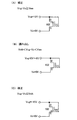
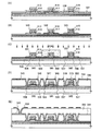
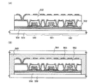
102 トランジスタ
103 グラフ
104 グラフ
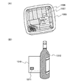
201 集積回路
202 アンテナ
203 基板
204 カバー材
205 集積回路
206 アンテナ
207 カバー材
208 基板
301 集積回路
302 アンテナ
303 整流回路
304 クロック生成回路
305 変調回路
306 復調回路
307 リミッタ
308 論理回路部
Claims (14)
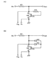
- 絶縁膜を間に挟んで重なって設けられたフローティングゲート及びコントロールゲートを有するトランジスタと、アンテナと、入力端子と、出力端子と、前記フローティングゲートに蓄積される電荷量を制御するための端子とを有し、
前記トランジスタのドレインは、前記トランジスタの前記コントロールゲート、前記入力端子、前記出力端子及び前記フローティングゲートに蓄積される電荷量を制御するための端子に電気的に接続され、
前記トランジスタのソースには一定の電圧が供給され、
前記入力端子は前記アンテナに電気的に接続されていることを特徴とする半導体装置。 - 請求項1において、前記トランジスタの前記ドレインと前記コントロールゲートの間に抵抗を有することを特徴とする半導体装置。
- 請求項1において、前記トランジスタの前記ドレインと前記コントロールゲートの間に、順方向電流の向きが互いに逆になるように第1のダイオードと第2のダイオードが並列に接続されていることを特徴とする半導体装置。
- 請求項1乃至3のいずれか一において、前記トランジスタは薄膜トランジスタであることを特徴とする半導体装置。
- 第1のトランジスタと、絶縁膜を間に挟んで設けられたフローティングゲート及びコントロールゲートを有する第2のトランジスタと、アンテナと、入力端子と、出力端子と、前記フローティングゲートに蓄積される電荷量を制御するための端子とを有し、
前記第1のトランジスタのドレインは、前記第1のトランジスタのゲート、前記入力端子及び前記出力端子に電気的に接続され、
前記第2のトランジスタのドレインは、前記第1のトランジスタのソース、前記第2のトランジスタのコントロールゲート及び前記フローティングゲートに蓄積される電荷量を制御するための端子に電気的に接続され、
前記第2のトランジスタのソースには一定の電圧が供給され、
前記入力端子は前記アンテナに電気的に接続されていることを特徴とする半導体装置。 - 絶縁膜を間に挟んで設けられたフローティングゲート及びコントロールゲートを有する第1のトランジスタと、第2のトランジスタと、アンテナと、入力端子と、出力端子と、前記フローティングゲートに蓄積される電荷量を制御するための端子とを有し、
前記第1のトランジスタのドレインは、前記第1のトランジスタのコントロールゲート、前記入力端子、前記出力端子及び前記フローティングゲートに蓄積される電荷量を制御するための端子に電気的に接続され、
前記第2のトランジスタのドレインは、前記第1のトランジスタのソース及び前記第2のトランジスタのゲートに電気的に接続され、
前記第2のトランジスタのソースには一定の電圧が供給され、
前記入力端子は前記アンテナに電気的に接続されていることを特徴とする半導体装置。 - 第1の絶縁膜を間に挟んで設けられた第1のフローティングゲート及び第1のコントロールゲートを有する第1のトランジスタと、第2の絶縁膜を間に挟んで設けられた第2のフローティングゲート及び第2のコントロールゲートを有する第2のトランジスタと、アンテナと、入力端子と、出力端子と、前記第1のフローティングゲートに蓄積される電荷量を制御するための端子と、前記第2のフローティングゲートに蓄積される電荷量を制御するための端子とを有し、
前記第1のトランジスタのドレインは、前記第1のコントロールゲート、前記入力端子、前記出力端子及び前記第1のフローティングゲートに蓄積される電荷量を制御するための端子に電気的に接続され、
前記第2のトランジスタのドレインは、前記第1のトランジスタのソース、前記第2のコントロールゲート及び前記第2のフローティングゲートに蓄積される電荷量を制御するための端子に電気的に接続され、
前記第2のトランジスタのソースには一定の電圧が供給され、
前記入力端子は前記アンテナに電気的に接続されていることを特徴とする半導体装置。 - 集積回路と、前記集積回路に電気的に接続されたアンテナとを有し、
前記集積回路は、第1のトランジスタと、絶縁膜を間に挟んで設けられたフローティングゲート及びコントロールゲートを有する第2のトランジスタと、入力端子と、出力端子と、前記フローティングゲートに蓄積される電荷量を制御するための端子とを有し、
前記第1のトランジスタのドレインは、前記第1のトランジスタのゲート、前記入力端子及び前記出力端子に電気的に接続され、
前記第2のトランジスタのドレインは、前記第1のトランジスタのソース、前記第2のトランジスタのコントロールゲート及び前記フローティングゲートに蓄積される電荷量を制御するための端子に電気的に接続され、
前記第2のトランジスタのソースには一定の電圧が供給され、
前記入力端子は前記アンテナに電気的に接続されていることを特徴とする半導体装置。 - 集積回路と、前記集積回路に電気的に接続されたアンテナとを有し、
前記集積回路は、第1のトランジスタと、絶縁膜を間に挟んで設けられたフローティングゲート及びコントロールゲートを有する第2のトランジスタと、前記第2のトランジスタの電圧を制御するためのパルス生成回路と、前記パルス生成回路への電源電圧の供給を行うための昇圧回路とを有し、
前記第1のトランジスタのドレインは、前記第1のトランジスタのゲート、前記入力端子及び前記出力端子に電気的に接続され、
前記第2のトランジスタのドレインは、前記第1のトランジスタのソース及び前記パルス生成回路に電気的に接続され、
前記第2のトランジスタのコントロールゲートは前記パルス生成回路に電気的に接続され、
前記第2のトランジスタのソースには一定の電圧が供給されるとともに前記パルス生成回路に電気的に接続され、
前記入力端子はアンテナに電気的に接続されていることを特徴とする半導体装置。 - 請求項5又は8において、前記第2のトランジスタの前記ドレインと前記コントロールゲートの間に抵抗、又は順方向電流の向きが互いに逆になるように並列に接続された第1のダイオードと第2のダイオードを有することを特徴とする半導体装置。
- 請求項6において、前記第1のトランジスタの前記ドレインと前記コントロールゲートの間に抵抗、又は順方向電流の向きが互いに逆になるように並列に接続された第1のダイオードと第2のダイオードを有することを特徴とする半導体装置。
- 請求項7において、前記第1のトランジスタの前記ドレインと前記第1のコントロールゲートの間と、前記第2のトランジスタの前記ドレインと前記第2のコントロールゲートの間に、抵抗、又は順方向電流の向きが互いに逆になるように並列に接続された第1のダイオードと第2のダイオードを有することを特徴とする半導体装置。
- 請求項5乃至12のいずれか一において、前記第1のトランジスタと前記第2のトランジスタは、順方向電流の向きが同じであることを特徴とする半導体装置。
- 請求項5乃至13のいずれか一において、前記第1のトランジスタ及び前記第2のトランジスタは薄膜トランジスタであることを特徴とする半導体装置
Priority Applications (1)
| Application Number | Priority Date | Filing Date | Title |
|---|---|---|---|
| JP2005111799A JP5041672B2 (ja) | 2004-04-09 | 2005-04-08 | 半導体装置 |
Applications Claiming Priority (3)
| Application Number | Priority Date | Filing Date | Title |
|---|---|---|---|
| JP2004115467 | 2004-04-09 | ||
| JP2004115467 | 2004-04-09 | ||
| JP2005111799A JP5041672B2 (ja) | 2004-04-09 | 2005-04-08 | 半導体装置 |
Publications (3)
| Publication Number | Publication Date |
|---|---|
| JP2005322899A JP2005322899A (ja) | 2005-11-17 |
| JP2005322899A5 JP2005322899A5 (ja) | 2008-05-15 |
| JP5041672B2 true JP5041672B2 (ja) | 2012-10-03 |
Family
ID=35469907
Family Applications (1)
| Application Number | Title | Priority Date | Filing Date |
|---|---|---|---|
| JP2005111799A Expired - Fee Related JP5041672B2 (ja) | 2004-04-09 | 2005-04-08 | 半導体装置 |
Country Status (1)
| Country | Link |
|---|---|
| JP (1) | JP5041672B2 (ja) |
Families Citing this family (10)
| Publication number | Priority date | Publication date | Assignee | Title |
|---|---|---|---|---|
| KR101424524B1 (ko) | 2005-05-30 | 2014-08-01 | 가부시키가이샤 한도오따이 에네루기 켄큐쇼 | 반도체 장치 |
| JP2007241997A (ja) * | 2006-02-10 | 2007-09-20 | Semiconductor Energy Lab Co Ltd | 半導体装置 |
| TWI411964B (zh) | 2006-02-10 | 2013-10-11 | Semiconductor Energy Lab | 半導體裝置 |
| EP1909384A3 (en) | 2006-10-06 | 2015-11-25 | Semiconductor Energy Laboratory Co., Ltd. | Rectifier circuit with variable capacitor, semiconductor device using the circuit, and driving method therefor |
| IN2012DN05057A (ja) | 2009-12-28 | 2015-10-09 | Semiconductor Energy Lab | |
| WO2011114866A1 (en) | 2010-03-17 | 2011-09-22 | Semiconductor Energy Laboratory Co., Ltd. | Memory device and semiconductor device |
| TWI688047B (zh) | 2010-08-06 | 2020-03-11 | 半導體能源研究所股份有限公司 | 半導體裝置 |
| KR102334169B1 (ko) | 2010-08-27 | 2021-12-01 | 가부시키가이샤 한도오따이 에네루기 켄큐쇼 | 기억 장치, 반도체 장치 |
| US9024317B2 (en) | 2010-12-24 | 2015-05-05 | Semiconductor Energy Laboratory Co., Ltd. | Semiconductor circuit, method for driving the same, storage device, register circuit, display device, and electronic device |
| JP5993141B2 (ja) | 2010-12-28 | 2016-09-14 | 株式会社半導体エネルギー研究所 | 記憶装置 |
Family Cites Families (6)
| Publication number | Priority date | Publication date | Assignee | Title |
|---|---|---|---|---|
| JPS53126567U (ja) * | 1977-03-15 | 1978-10-07 | ||
| JPS6187373A (ja) * | 1984-10-05 | 1986-05-02 | Nec Corp | 絶縁ゲ−ト保護半導体装置 |
| US5272586A (en) * | 1991-01-29 | 1993-12-21 | National Semiconductor Corporation | Technique for improving ESD immunity |
| JP3348734B2 (ja) * | 1992-07-30 | 2002-11-20 | ソニー株式会社 | 保護回路 |
| JPH09293835A (ja) * | 1996-04-30 | 1997-11-11 | Nkk Corp | 入力保護回路 |
| WO2000044049A1 (fr) * | 1999-01-19 | 2000-07-27 | Seiko Epson Corporation | Circuit de protection contre l'electricite statique, et circuit integre |
-
2005
- 2005-04-08 JP JP2005111799A patent/JP5041672B2/ja not_active Expired - Fee Related
Also Published As
| Publication number | Publication date |
|---|---|
| JP2005322899A (ja) | 2005-11-17 |
Similar Documents
| Publication | Publication Date | Title |
|---|---|---|
| US8054121B2 (en) | Limiter and semiconductor device using the same | |
| JP5041672B2 (ja) | 半導体装置 | |
| US8159043B2 (en) | Semiconductor device | |
| US8049669B2 (en) | Semiconductor device comprising circuit between first and second conducting wires | |
| US8030745B2 (en) | ID chip and IC card | |
| US8289164B2 (en) | Semiconductor device and manufacturing method thereof | |
| US7994617B2 (en) | Semiconductor device | |
| US7732263B2 (en) | Semiconductor device | |
| JP4566794B2 (ja) | 半導体装置 | |
| JP4989854B2 (ja) | 半導体装置の作製方法 | |
| JP4718863B2 (ja) | 半導体装置及び半導体装置の作製方法 | |
| JP4545617B2 (ja) | 半導体装置 | |
| JP2005229098A (ja) | 半導体装置及び半導体装置の作製方法 |
Legal Events
| Date | Code | Title | Description |
|---|---|---|---|
| A521 | Request for written amendment filed |
Free format text: JAPANESE INTERMEDIATE CODE: A523 Effective date: 20080401 |
|
| A621 | Written request for application examination |
Free format text: JAPANESE INTERMEDIATE CODE: A621 Effective date: 20080401 |
|
| A977 | Report on retrieval |
Free format text: JAPANESE INTERMEDIATE CODE: A971007 Effective date: 20110623 |
|
| A131 | Notification of reasons for refusal |
Free format text: JAPANESE INTERMEDIATE CODE: A131 Effective date: 20110628 |
|
| A521 | Request for written amendment filed |
Free format text: JAPANESE INTERMEDIATE CODE: A523 Effective date: 20110822 |
|
| A131 | Notification of reasons for refusal |
Free format text: JAPANESE INTERMEDIATE CODE: A131 Effective date: 20120117 |
|
| A521 | Request for written amendment filed |
Free format text: JAPANESE INTERMEDIATE CODE: A523 Effective date: 20120306 |
|
| TRDD | Decision of grant or rejection written | ||
| A01 | Written decision to grant a patent or to grant a registration (utility model) |
Free format text: JAPANESE INTERMEDIATE CODE: A01 Effective date: 20120703 |
|
| A01 | Written decision to grant a patent or to grant a registration (utility model) |
Free format text: JAPANESE INTERMEDIATE CODE: A01 |
|
| A61 | First payment of annual fees (during grant procedure) |
Free format text: JAPANESE INTERMEDIATE CODE: A61 Effective date: 20120710 |
|
| R150 | Certificate of patent or registration of utility model |
Free format text: JAPANESE INTERMEDIATE CODE: R150 |
|
| FPAY | Renewal fee payment (event date is renewal date of database) |
Free format text: PAYMENT UNTIL: 20150720 Year of fee payment: 3 |
|
| FPAY | Renewal fee payment (event date is renewal date of database) |
Free format text: PAYMENT UNTIL: 20150720 Year of fee payment: 3 |
|
| R250 | Receipt of annual fees |
Free format text: JAPANESE INTERMEDIATE CODE: R250 |
|
| R250 | Receipt of annual fees |
Free format text: JAPANESE INTERMEDIATE CODE: R250 |
|
| R250 | Receipt of annual fees |
Free format text: JAPANESE INTERMEDIATE CODE: R250 |
|
| LAPS | Cancellation because of no payment of annual fees |