JP5041672B2 - Semiconductor device - Google Patents
Semiconductor device Download PDFInfo
- Publication number
- JP5041672B2 JP5041672B2 JP2005111799A JP2005111799A JP5041672B2 JP 5041672 B2 JP5041672 B2 JP 5041672B2 JP 2005111799 A JP2005111799 A JP 2005111799A JP 2005111799 A JP2005111799 A JP 2005111799A JP 5041672 B2 JP5041672 B2 JP 5041672B2
- Authority
- JP
- Japan
- Prior art keywords
- transistor
- voltage
- drain
- gate
- antenna
- Prior art date
- Legal status (The legal status is an assumption and is not a legal conclusion. Google has not performed a legal analysis and makes no representation as to the accuracy of the status listed.)
- Expired - Fee Related
Links
- 239000004065 semiconductor Substances 0.000 title claims description 186
- 239000010408 film Substances 0.000 claims description 317
- 238000007667 floating Methods 0.000 claims description 56
- 239000010409 thin film Substances 0.000 claims description 3
- 239000000758 substrate Substances 0.000 description 114
- 238000000034 method Methods 0.000 description 77
- 239000011229 interlayer Substances 0.000 description 54
- 239000000463 material Substances 0.000 description 48
- 239000000853 adhesive Substances 0.000 description 36
- 230000001070 adhesive effect Effects 0.000 description 36
- 239000007789 gas Substances 0.000 description 34
- 239000010410 layer Substances 0.000 description 30
- 238000004519 manufacturing process Methods 0.000 description 28
- 239000011347 resin Substances 0.000 description 27
- 229920005989 resin Polymers 0.000 description 27
- 238000005530 etching Methods 0.000 description 26
- 238000010586 diagram Methods 0.000 description 24
- 239000011521 glass Substances 0.000 description 23
- 229910052581 Si3N4 Inorganic materials 0.000 description 22
- XUIMIQQOPSSXEZ-UHFFFAOYSA-N Silicon Chemical compound [Si] XUIMIQQOPSSXEZ-UHFFFAOYSA-N 0.000 description 22
- 229910052710 silicon Inorganic materials 0.000 description 22
- 239000010703 silicon Substances 0.000 description 22
- VYPSYNLAJGMNEJ-UHFFFAOYSA-N silicon dioxide Inorganic materials O=[Si]=O VYPSYNLAJGMNEJ-UHFFFAOYSA-N 0.000 description 22
- HQVNEWCFYHHQES-UHFFFAOYSA-N silicon nitride Chemical compound N12[Si]34N5[Si]62N3[Si]51N64 HQVNEWCFYHHQES-UHFFFAOYSA-N 0.000 description 22
- 229910052814 silicon oxide Inorganic materials 0.000 description 20
- 239000012535 impurity Substances 0.000 description 18
- 239000002585 base Substances 0.000 description 17
- UFHFLCQGNIYNRP-UHFFFAOYSA-N Hydrogen Chemical compound [H][H] UFHFLCQGNIYNRP-UHFFFAOYSA-N 0.000 description 15
- 239000001257 hydrogen Substances 0.000 description 15
- 229910052739 hydrogen Inorganic materials 0.000 description 15
- 230000006870 function Effects 0.000 description 13
- 229910052751 metal Inorganic materials 0.000 description 13
- 239000002184 metal Substances 0.000 description 13
- 230000001965 increasing effect Effects 0.000 description 12
- 230000002829 reductive effect Effects 0.000 description 12
- 239000013078 crystal Substances 0.000 description 11
- 230000000670 limiting effect Effects 0.000 description 11
- 150000002736 metal compounds Chemical class 0.000 description 11
- 238000012937 correction Methods 0.000 description 10
- KPUWHANPEXNPJT-UHFFFAOYSA-N disiloxane Chemical class [SiH3]O[SiH3] KPUWHANPEXNPJT-UHFFFAOYSA-N 0.000 description 10
- 238000005268 plasma chemical vapour deposition Methods 0.000 description 10
- 230000008569 process Effects 0.000 description 10
- -1 halogen fluoride Chemical class 0.000 description 9
- 238000010438 heat treatment Methods 0.000 description 8
- 230000015654 memory Effects 0.000 description 8
- 238000007639 printing Methods 0.000 description 8
- 238000000926 separation method Methods 0.000 description 8
- 229910021332 silicide Inorganic materials 0.000 description 8
- FVBUAEGBCNSCDD-UHFFFAOYSA-N silicide(4-) Chemical compound [Si-4] FVBUAEGBCNSCDD-UHFFFAOYSA-N 0.000 description 8
- 238000002425 crystallisation Methods 0.000 description 7
- 238000005499 laser crystallization Methods 0.000 description 7
- 238000000059 patterning Methods 0.000 description 7
- 239000011241 protective layer Substances 0.000 description 7
- 230000008901 benefit Effects 0.000 description 6
- 239000004020 conductor Substances 0.000 description 6
- 239000002784 hot electron Substances 0.000 description 6
- 238000002347 injection Methods 0.000 description 6
- 239000007924 injection Substances 0.000 description 6
- 229920003023 plastic Polymers 0.000 description 6
- 239000004033 plastic Substances 0.000 description 6
- 125000001424 substituent group Chemical group 0.000 description 6
- 229910052715 tantalum Inorganic materials 0.000 description 6
- MZLGASXMSKOWSE-UHFFFAOYSA-N tantalum nitride Chemical compound [Ta]#N MZLGASXMSKOWSE-UHFFFAOYSA-N 0.000 description 6
- 239000010936 titanium Substances 0.000 description 6
- 239000004642 Polyimide Substances 0.000 description 5
- 230000015556 catabolic process Effects 0.000 description 5
- 239000000460 chlorine Substances 0.000 description 5
- 230000000694 effects Effects 0.000 description 5
- 229910052736 halogen Inorganic materials 0.000 description 5
- 230000010355 oscillation Effects 0.000 description 5
- 239000005022 packaging material Substances 0.000 description 5
- 229920001721 polyimide Polymers 0.000 description 5
- 238000004544 sputter deposition Methods 0.000 description 5
- GUVRBAGPIYLISA-UHFFFAOYSA-N tantalum atom Chemical compound [Ta] GUVRBAGPIYLISA-UHFFFAOYSA-N 0.000 description 5
- XKRFYHLGVUSROY-UHFFFAOYSA-N Argon Chemical compound [Ar] XKRFYHLGVUSROY-UHFFFAOYSA-N 0.000 description 4
- IJGRMHOSHXDMSA-UHFFFAOYSA-N Atomic nitrogen Chemical compound N#N IJGRMHOSHXDMSA-UHFFFAOYSA-N 0.000 description 4
- KRHYYFGTRYWZRS-UHFFFAOYSA-N Fluorane Chemical compound F KRHYYFGTRYWZRS-UHFFFAOYSA-N 0.000 description 4
- 229910052783 alkali metal Inorganic materials 0.000 description 4
- 150000001340 alkali metals Chemical class 0.000 description 4
- 229910052784 alkaline earth metal Inorganic materials 0.000 description 4
- 150000001342 alkaline earth metals Chemical class 0.000 description 4
- 229910021417 amorphous silicon Inorganic materials 0.000 description 4
- 230000003197 catalytic effect Effects 0.000 description 4
- 238000004891 communication Methods 0.000 description 4
- 125000001153 fluoro group Chemical group F* 0.000 description 4
- 238000005984 hydrogenation reaction Methods 0.000 description 4
- 229910052759 nickel Inorganic materials 0.000 description 4
- PXHVJJICTQNCMI-UHFFFAOYSA-N nickel Substances [Ni] PXHVJJICTQNCMI-UHFFFAOYSA-N 0.000 description 4
- 125000000962 organic group Chemical group 0.000 description 4
- 238000002161 passivation Methods 0.000 description 4
- 238000000206 photolithography Methods 0.000 description 4
- 229910052718 tin Inorganic materials 0.000 description 4
- 229910052719 titanium Inorganic materials 0.000 description 4
- OKTJSMMVPCPJKN-UHFFFAOYSA-N Carbon Chemical compound [C] OKTJSMMVPCPJKN-UHFFFAOYSA-N 0.000 description 3
- 239000004593 Epoxy Substances 0.000 description 3
- 239000004952 Polyamide Substances 0.000 description 3
- ATJFFYVFTNAWJD-UHFFFAOYSA-N Tin Chemical compound [Sn] ATJFFYVFTNAWJD-UHFFFAOYSA-N 0.000 description 3
- 230000001133 acceleration Effects 0.000 description 3
- NIXOWILDQLNWCW-UHFFFAOYSA-N acrylic acid group Chemical group C(C=C)(=O)O NIXOWILDQLNWCW-UHFFFAOYSA-N 0.000 description 3
- 238000004380 ashing Methods 0.000 description 3
- 229910052799 carbon Inorganic materials 0.000 description 3
- 229910052802 copper Inorganic materials 0.000 description 3
- 230000007547 defect Effects 0.000 description 3
- 230000002950 deficient Effects 0.000 description 3
- 238000009826 distribution Methods 0.000 description 3
- 230000005674 electromagnetic induction Effects 0.000 description 3
- 229910052737 gold Inorganic materials 0.000 description 3
- 239000001307 helium Substances 0.000 description 3
- 229910052734 helium Inorganic materials 0.000 description 3
- SWQJXJOGLNCZEY-UHFFFAOYSA-N helium atom Chemical compound [He] SWQJXJOGLNCZEY-UHFFFAOYSA-N 0.000 description 3
- 230000001678 irradiating effect Effects 0.000 description 3
- 229910044991 metal oxide Inorganic materials 0.000 description 3
- 150000004706 metal oxides Chemical class 0.000 description 3
- 229910052698 phosphorus Inorganic materials 0.000 description 3
- 229920002647 polyamide Polymers 0.000 description 3
- 239000002356 single layer Substances 0.000 description 3
- 238000004528 spin coating Methods 0.000 description 3
- 229920001187 thermosetting polymer Polymers 0.000 description 3
- 229910052721 tungsten Inorganic materials 0.000 description 3
- 229920000178 Acrylic resin Polymers 0.000 description 2
- 239000004925 Acrylic resin Substances 0.000 description 2
- 229910018125 Al-Si Inorganic materials 0.000 description 2
- 229910018520 Al—Si Inorganic materials 0.000 description 2
- OAICVXFJPJFONN-UHFFFAOYSA-N Phosphorus Chemical compound [P] OAICVXFJPJFONN-UHFFFAOYSA-N 0.000 description 2
- 239000004696 Poly ether ether ketone Substances 0.000 description 2
- 239000004697 Polyetherimide Substances 0.000 description 2
- 239000004743 Polypropylene Substances 0.000 description 2
- 229910000577 Silicon-germanium Inorganic materials 0.000 description 2
- BOTDANWDWHJENH-UHFFFAOYSA-N Tetraethyl orthosilicate Chemical compound CCO[Si](OCC)(OCC)OCC BOTDANWDWHJENH-UHFFFAOYSA-N 0.000 description 2
- LEVVHYCKPQWKOP-UHFFFAOYSA-N [Si].[Ge] Chemical compound [Si].[Ge] LEVVHYCKPQWKOP-UHFFFAOYSA-N 0.000 description 2
- 230000002411 adverse Effects 0.000 description 2
- 125000000217 alkyl group Chemical group 0.000 description 2
- 239000005407 aluminoborosilicate glass Substances 0.000 description 2
- 238000000137 annealing Methods 0.000 description 2
- 229910052786 argon Inorganic materials 0.000 description 2
- 150000004945 aromatic hydrocarbons Chemical class 0.000 description 2
- 229910052785 arsenic Inorganic materials 0.000 description 2
- 239000012298 atmosphere Substances 0.000 description 2
- 125000004429 atom Chemical group 0.000 description 2
- 229910052788 barium Inorganic materials 0.000 description 2
- DSAJWYNOEDNPEQ-UHFFFAOYSA-N barium atom Chemical compound [Ba] DSAJWYNOEDNPEQ-UHFFFAOYSA-N 0.000 description 2
- 230000005540 biological transmission Effects 0.000 description 2
- 239000005388 borosilicate glass Substances 0.000 description 2
- 239000002775 capsule Substances 0.000 description 2
- 230000008859 change Effects 0.000 description 2
- 229910052804 chromium Inorganic materials 0.000 description 2
- 238000010168 coupling process Methods 0.000 description 2
- 238000000354 decomposition reaction Methods 0.000 description 2
- 239000000428 dust Substances 0.000 description 2
- 150000002367 halogens Chemical class 0.000 description 2
- 229910010272 inorganic material Inorganic materials 0.000 description 2
- 239000011147 inorganic material Substances 0.000 description 2
- 229910052742 iron Inorganic materials 0.000 description 2
- 229910052743 krypton Inorganic materials 0.000 description 2
- DNNSSWSSYDEUBZ-UHFFFAOYSA-N krypton atom Chemical compound [Kr] DNNSSWSSYDEUBZ-UHFFFAOYSA-N 0.000 description 2
- 239000007788 liquid Substances 0.000 description 2
- 229910052754 neon Inorganic materials 0.000 description 2
- GKAOGPIIYCISHV-UHFFFAOYSA-N neon atom Chemical compound [Ne] GKAOGPIIYCISHV-UHFFFAOYSA-N 0.000 description 2
- 229910052757 nitrogen Inorganic materials 0.000 description 2
- 239000012299 nitrogen atmosphere Substances 0.000 description 2
- 230000003287 optical effect Effects 0.000 description 2
- 239000011368 organic material Substances 0.000 description 2
- JMANVNJQNLATNU-UHFFFAOYSA-N oxalonitrile Chemical compound N#CC#N JMANVNJQNLATNU-UHFFFAOYSA-N 0.000 description 2
- 239000002245 particle Substances 0.000 description 2
- 239000011574 phosphorus Substances 0.000 description 2
- 229920002492 poly(sulfone) Polymers 0.000 description 2
- 229920001230 polyarylate Polymers 0.000 description 2
- 229920001707 polybutylene terephthalate Polymers 0.000 description 2
- 229920002530 polyetherether ketone Polymers 0.000 description 2
- 229920001601 polyetherimide Polymers 0.000 description 2
- 229920000139 polyethylene terephthalate Polymers 0.000 description 2
- 239000005020 polyethylene terephthalate Substances 0.000 description 2
- 229920001155 polypropylene Polymers 0.000 description 2
- 239000010453 quartz Substances 0.000 description 2
- 229910052709 silver Inorganic materials 0.000 description 2
- 239000002904 solvent Substances 0.000 description 2
- 238000002230 thermal chemical vapour deposition Methods 0.000 description 2
- WFKWXMTUELFFGS-UHFFFAOYSA-N tungsten Chemical compound [W] WFKWXMTUELFFGS-UHFFFAOYSA-N 0.000 description 2
- 239000010937 tungsten Substances 0.000 description 2
- 230000005641 tunneling Effects 0.000 description 2
- 238000001039 wet etching Methods 0.000 description 2
- 229910052725 zinc Inorganic materials 0.000 description 2
- NIXOWILDQLNWCW-UHFFFAOYSA-M Acrylate Chemical compound [O-]C(=O)C=C NIXOWILDQLNWCW-UHFFFAOYSA-M 0.000 description 1
- ZOXJGFHDIHLPTG-UHFFFAOYSA-N Boron Chemical compound [B] ZOXJGFHDIHLPTG-UHFFFAOYSA-N 0.000 description 1
- JOYRKODLDBILNP-UHFFFAOYSA-N Ethyl urethane Chemical compound CCOC(N)=O JOYRKODLDBILNP-UHFFFAOYSA-N 0.000 description 1
- 229910005883 NiSi Inorganic materials 0.000 description 1
- 239000004677 Nylon Substances 0.000 description 1
- 229920012266 Poly(ether sulfone) PES Polymers 0.000 description 1
- 239000004698 Polyethylene Substances 0.000 description 1
- 239000004793 Polystyrene Substances 0.000 description 1
- 238000001237 Raman spectrum Methods 0.000 description 1
- 229910003902 SiCl 4 Inorganic materials 0.000 description 1
- 229910004205 SiNX Inorganic materials 0.000 description 1
- 229910002808 Si–O–Si Inorganic materials 0.000 description 1
- GWEVSGVZZGPLCZ-UHFFFAOYSA-N Titan oxide Chemical compound O=[Ti]=O GWEVSGVZZGPLCZ-UHFFFAOYSA-N 0.000 description 1
- RTAQQCXQSZGOHL-UHFFFAOYSA-N Titanium Chemical compound [Ti] RTAQQCXQSZGOHL-UHFFFAOYSA-N 0.000 description 1
- 238000002441 X-ray diffraction Methods 0.000 description 1
- GDFCWFBWQUEQIJ-UHFFFAOYSA-N [B].[P] Chemical compound [B].[P] GDFCWFBWQUEQIJ-UHFFFAOYSA-N 0.000 description 1
- 238000009825 accumulation Methods 0.000 description 1
- XECAHXYUAAWDEL-UHFFFAOYSA-N acrylonitrile butadiene styrene Chemical compound C=CC=C.C=CC#N.C=CC1=CC=CC=C1 XECAHXYUAAWDEL-UHFFFAOYSA-N 0.000 description 1
- 239000004676 acrylonitrile butadiene styrene Substances 0.000 description 1
- 229920000122 acrylonitrile butadiene styrene Polymers 0.000 description 1
- 150000001298 alcohols Chemical class 0.000 description 1
- 229910052782 aluminium Inorganic materials 0.000 description 1
- PNEYBMLMFCGWSK-UHFFFAOYSA-N aluminium oxide Inorganic materials [O-2].[O-2].[O-2].[Al+3].[Al+3] PNEYBMLMFCGWSK-UHFFFAOYSA-N 0.000 description 1
- RQNWIZPPADIBDY-UHFFFAOYSA-N arsenic atom Chemical compound [As] RQNWIZPPADIBDY-UHFFFAOYSA-N 0.000 description 1
- 238000001505 atmospheric-pressure chemical vapour deposition Methods 0.000 description 1
- QVGXLLKOCUKJST-UHFFFAOYSA-N atomic oxygen Chemical compound [O] QVGXLLKOCUKJST-UHFFFAOYSA-N 0.000 description 1
- 230000002238 attenuated effect Effects 0.000 description 1
- 238000005452 bending Methods 0.000 description 1
- UMIVXZPTRXBADB-UHFFFAOYSA-N benzocyclobutene Chemical compound C1=CC=C2CCC2=C1 UMIVXZPTRXBADB-UHFFFAOYSA-N 0.000 description 1
- 230000033228 biological regulation Effects 0.000 description 1
- 229910052796 boron Inorganic materials 0.000 description 1
- 239000005380 borophosphosilicate glass Substances 0.000 description 1
- 239000000969 carrier Substances 0.000 description 1
- 239000000919 ceramic Substances 0.000 description 1
- 238000006243 chemical reaction Methods 0.000 description 1
- SLLGVCUQYRMELA-UHFFFAOYSA-N chlorosilicon Chemical compound Cl[Si] SLLGVCUQYRMELA-UHFFFAOYSA-N 0.000 description 1
- 238000004140 cleaning Methods 0.000 description 1
- 239000011248 coating agent Substances 0.000 description 1
- 238000000576 coating method Methods 0.000 description 1
- PMHQVHHXPFUNSP-UHFFFAOYSA-M copper(1+);methylsulfanylmethane;bromide Chemical compound Br[Cu].CSC PMHQVHHXPFUNSP-UHFFFAOYSA-M 0.000 description 1
- 238000005336 cracking Methods 0.000 description 1
- 230000008025 crystallization Effects 0.000 description 1
- 238000007865 diluting Methods 0.000 description 1
- 238000010790 dilution Methods 0.000 description 1
- 239000012895 dilution Substances 0.000 description 1
- 238000003618 dip coating Methods 0.000 description 1
- 238000001312 dry etching Methods 0.000 description 1
- 230000002708 enhancing effect Effects 0.000 description 1
- 238000001704 evaporation Methods 0.000 description 1
- 239000000945 filler Substances 0.000 description 1
- 238000011049 filling Methods 0.000 description 1
- 235000013305 food Nutrition 0.000 description 1
- SCCCLDWUZODEKG-UHFFFAOYSA-N germanide Chemical compound [GeH3-] SCCCLDWUZODEKG-UHFFFAOYSA-N 0.000 description 1
- 229910052732 germanium Inorganic materials 0.000 description 1
- GNPVGFCGXDBREM-UHFFFAOYSA-N germanium atom Chemical compound [Ge] GNPVGFCGXDBREM-UHFFFAOYSA-N 0.000 description 1
- 239000010931 gold Substances 0.000 description 1
- 239000011261 inert gas Substances 0.000 description 1
- 238000009413 insulation Methods 0.000 description 1
- 238000010030 laminating Methods 0.000 description 1
- 238000004518 low pressure chemical vapour deposition Methods 0.000 description 1
- 229910052748 manganese Inorganic materials 0.000 description 1
- 239000002923 metal particle Substances 0.000 description 1
- 150000002739 metals Chemical class 0.000 description 1
- 229910021424 microcrystalline silicon Inorganic materials 0.000 description 1
- 238000002156 mixing Methods 0.000 description 1
- 230000004048 modification Effects 0.000 description 1
- 238000012986 modification Methods 0.000 description 1
- 229910052750 molybdenum Inorganic materials 0.000 description 1
- 229910021421 monocrystalline silicon Inorganic materials 0.000 description 1
- 229910021334 nickel silicide Inorganic materials 0.000 description 1
- RUFLMLWJRZAWLJ-UHFFFAOYSA-N nickel silicide Chemical compound [Ni]=[Si]=[Ni] RUFLMLWJRZAWLJ-UHFFFAOYSA-N 0.000 description 1
- 150000004767 nitrides Chemical class 0.000 description 1
- 229920001778 nylon Polymers 0.000 description 1
- 238000007645 offset printing Methods 0.000 description 1
- 230000003647 oxidation Effects 0.000 description 1
- 238000007254 oxidation reaction Methods 0.000 description 1
- TWNQGVIAIRXVLR-UHFFFAOYSA-N oxo(oxoalumanyloxy)alumane Chemical compound O=[Al]O[Al]=O TWNQGVIAIRXVLR-UHFFFAOYSA-N 0.000 description 1
- 239000001301 oxygen Substances 0.000 description 1
- 229910052760 oxygen Inorganic materials 0.000 description 1
- 229910052763 palladium Inorganic materials 0.000 description 1
- 238000001020 plasma etching Methods 0.000 description 1
- 238000009832 plasma treatment Methods 0.000 description 1
- 238000007747 plating Methods 0.000 description 1
- 229920000636 poly(norbornene) polymer Polymers 0.000 description 1
- 239000004417 polycarbonate Substances 0.000 description 1
- 229920000515 polycarbonate Polymers 0.000 description 1
- 229910021420 polycrystalline silicon Inorganic materials 0.000 description 1
- 229920000728 polyester Polymers 0.000 description 1
- 229920000573 polyethylene Polymers 0.000 description 1
- 239000011112 polyethylene naphthalate Substances 0.000 description 1
- 229920002223 polystyrene Polymers 0.000 description 1
- 229920002689 polyvinyl acetate Polymers 0.000 description 1
- 239000011118 polyvinyl acetate Substances 0.000 description 1
- 239000004800 polyvinyl chloride Substances 0.000 description 1
- 229920000915 polyvinyl chloride Polymers 0.000 description 1
- 238000003825 pressing Methods 0.000 description 1
- 238000012545 processing Methods 0.000 description 1
- 238000003672 processing method Methods 0.000 description 1
- 230000005855 radiation Effects 0.000 description 1
- 230000004044 response Effects 0.000 description 1
- 230000002441 reversible effect Effects 0.000 description 1
- 229910052706 scandium Inorganic materials 0.000 description 1
- 238000007650 screen-printing Methods 0.000 description 1
- 230000008054 signal transmission Effects 0.000 description 1
- 229910000679 solder Inorganic materials 0.000 description 1
- 238000003980 solgel method Methods 0.000 description 1
- 239000000243 solution Substances 0.000 description 1
- 238000005507 spraying Methods 0.000 description 1
- 229910001220 stainless steel Inorganic materials 0.000 description 1
- 239000010935 stainless steel Substances 0.000 description 1
- 229920003002 synthetic resin Polymers 0.000 description 1
- 239000000057 synthetic resin Substances 0.000 description 1
- 239000012815 thermoplastic material Substances 0.000 description 1
- OGIDPMRJRNCKJF-UHFFFAOYSA-N titanium oxide Inorganic materials [Ti]=O OGIDPMRJRNCKJF-UHFFFAOYSA-N 0.000 description 1
- 230000007704 transition Effects 0.000 description 1
- JOHWNGGYGAVMGU-UHFFFAOYSA-N trifluorochlorine Chemical compound FCl(F)F JOHWNGGYGAVMGU-UHFFFAOYSA-N 0.000 description 1
- 229910052720 vanadium Inorganic materials 0.000 description 1
- 239000002699 waste material Substances 0.000 description 1
- XLYOFNOQVPJJNP-UHFFFAOYSA-N water Substances O XLYOFNOQVPJJNP-UHFFFAOYSA-N 0.000 description 1
Images


Description
本発明は、薄膜の半導体膜を用いて形成されたリミッタに関する。さらに本発明は、該リミッタを用いた、無線での通信が可能な半導体装置に関する。 The present invention relates to a limiter formed using a thin semiconductor film. Furthermore, the present invention relates to a semiconductor device capable of wireless communication using the limiter.
無線でデータの送受信が可能なIDチップ、ICカードなどの半導体装置は、様々な分野において実用化が進められており、新しい形態の通信情報端末としてさらなる市場の拡大が見込まれている。IDチップは、無線タグ、RFID(Radio frequency identification)タグ、ICタグとも呼ばれている。そしてIDチップとICカードは、アンテナと、半導体基板を用いて形成された集積回路とを有しているタイプが、現在実用化されている。 Semiconductor devices such as ID chips and IC cards that can transmit and receive data wirelessly have been put into practical use in various fields, and further expansion of the market is expected as a new type of communication information terminal. The ID chip is also called a wireless tag, an RFID (Radio frequency identification) tag, or an IC tag. As for the ID chip and the IC card, a type having an antenna and an integrated circuit formed using a semiconductor substrate is currently put into practical use.
IDチップまたはICカードは、電波を用いてリーダ/ライタとの間の通信を行なうことができる。具体的には、リーダ/ライタから発せられる電波によりアンテナに生じる交流の電圧(交流電圧)を用いて、集積回路を動作させ、また、集積回路から出力された信号を用いてアンテナに負荷変調を与えることで、リーダ/ライタに信号を送ることができる。 An ID chip or an IC card can communicate with a reader / writer using radio waves. Specifically, an integrated circuit is operated using an AC voltage (AC voltage) generated in an antenna by radio waves emitted from a reader / writer, and load modulation is performed on the antenna using a signal output from the integrated circuit. By giving, a signal can be sent to the reader / writer.
ところで、リーダ/ライタから発せられる電波の強度は規定により定められているため、IDチップまたはICカードのアンテナに生じる交流電圧の大きさは、通常、所定の範囲内に収められる。しかし、例えば外部の電子機器から発せられた不要輻射などにより、IDチップまたはICカードが規定を上回る強力な電波にさらされた場合、アンテナにおいて所定の範囲を逸脱するような過度に大きい交流電圧が生じてしまう。そして、この過度の交流電圧により集積回路内の半導体素子に流れる電流が急激に上昇すると、絶縁破壊により集積回路が破壊されてしまう恐れがある。 By the way, since the intensity of the radio wave emitted from the reader / writer is determined by regulations, the magnitude of the AC voltage generated in the antenna of the ID chip or the IC card is usually within a predetermined range. However, if the ID chip or IC card is exposed to a strong radio wave exceeding the standard due to, for example, unnecessary radiation emitted from an external electronic device, an excessively large AC voltage that deviates from a predetermined range in the antenna. It will occur. If the current flowing through the semiconductor elements in the integrated circuit is suddenly increased by the excessive alternating voltage, the integrated circuit may be destroyed due to dielectric breakdown.
特に近年は、微細化によって半導体素子の耐圧が低下の傾向にある。そのため、過電流保護の機能を有する回路をIDチップまたはICカードに設けることは、IDチップまたはICカードの信頼性向上のために非常に有効である。リミッタは、入力された電圧に関わらず出力される電圧を設定電圧(リミット電圧)以下に抑える振幅制限器であり、上述した過電流保護のために用いられる回路の一つである。 Particularly in recent years, the breakdown voltage of semiconductor elements tends to decrease due to miniaturization. Therefore, providing a circuit having an overcurrent protection function in the ID chip or IC card is very effective for improving the reliability of the ID chip or IC card. The limiter is an amplitude limiter that suppresses the output voltage to a set voltage (limit voltage) or less regardless of the input voltage, and is one of the circuits used for the overcurrent protection described above.
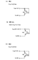
図20(A)に、一般的なリミッタの一例を、回路図で示す。1901は抵抗、1902はゲート(G)とドレイン(D)が接続(ダイオード接続)されたトランジスタに相当する。抵抗1901が有する2つの端子のうち、第1の端子には入力端子からの電圧Vinが供給されている。またトランジスタ1902のゲートとドレインは、抵抗1901の第2の端子に接続されており、トランジスタ1902のソース(S)にはグラウンド(GND)などの一定の電圧が供給されている。そして抵抗1901が有する2つの端子のうち、第2の端子の電圧は、リミッタの出力端子の電圧Voutに相当する。
FIG. 20A is a circuit diagram illustrating an example of a general limiter.
上記構成により、入力端子からの電圧Vinが過度に大きい場合でも、トランジスタ1902に順方向バイアスの電流が流れるため、出力端子の電圧Voutをリミット電圧以下に抑えることができる。ところが、このリミット電圧は、ダイオード接続されているトランジスタの特性に依存するため、リミット電圧を精度良く制御することが難しいという問題があった。
With the above structure, even when the voltage Vin from the input terminal is excessively large, a forward bias current flows through the
図20(B)に、トランジスタ1902のドレインとソース間の電圧Vdsと、ドレイン電流Idの関係を示す。順方向降下電圧Vfは、トランジスタ1902の閾値電圧Vthに依存する。そして、図20(A)に示すリミッタの場合、リミット電圧は順方向降下電圧Vfの値と等しくなるため、閾値電圧Vthのばらつきは、即、リミット電圧のばらつきとなって現れる。
FIG. 20B shows the relationship between the drain-source voltage Vds and the drain current Id of the
よって、トランジスタ1902の特性がばらつくと、リミッタの出力端子の電圧Voutを精度良く制御することが困難となり、集積回路を所望のスペックで動作させることができないばかりか、絶縁破壊により集積回路を破壊させてしまう恐れもある。
Therefore, if the characteristics of the
またその他の問題として、集積回路を形成するのに用いられている半導体基板は、ガラス基板などに比べて高価で、可撓性に乏しく、機械的強度が低いことが挙げられる。集積回路自体の面積を縮小化することで、機械的強度をある程度向上させることはできる。しかしこの場合、回路規模の確保が難しくなり、IDチップやICカードの用途が制限されるので好ましくない。従って集積回路の回路規模の確保を重要視すると、やみくもに集積回路の面積を縮小化することは妥当ではなく、機械的強度の向上にも限界が生じている。 Another problem is that a semiconductor substrate used for forming an integrated circuit is more expensive than a glass substrate, lacks flexibility, and has low mechanical strength. By reducing the area of the integrated circuit itself, the mechanical strength can be improved to some extent. However, in this case, it is difficult to ensure the circuit scale, and the use of the ID chip and the IC card is limited. Therefore, if it is important to secure the circuit scale of the integrated circuit, it is not appropriate to reduce the area of the integrated circuit, and there is a limit in improving the mechanical strength.
本発明は上記問題に鑑み、リミット電圧を制御良く制御することが可能なリミッタの提供を課題とする。また本発明は、リミット電圧を制御良く制御することが可能な半導体装置の提供を課題とする。さらに本発明は、該リミッタを用い、回路規模を抑えることなく集積回路の機械的強度を高めることができる半導体装置の提供を課題とする。また、本発明は安価な半導体装置の提供を課題とする。 In view of the above problems, an object of the present invention is to provide a limiter capable of controlling the limit voltage with good control. Another object of the present invention is to provide a semiconductor device capable of controlling the limit voltage with good control. Another object of the present invention is to provide a semiconductor device that can increase the mechanical strength of an integrated circuit using the limiter without reducing the circuit scale. Another object of the present invention is to provide an inexpensive semiconductor device.
本発明のリミッタは、浮遊ゲート(フローティングゲート)を有するスタックドゲート構造のトランジスタを、ダイオードとして用いることを特徴とする。 The limiter of the present invention is characterized in that a transistor having a stacked gate structure having a floating gate (floating gate) is used as a diode.
より具体的には、一対の不純物領域を有する半導体と、前記半導体上に形成された第1の絶縁膜と、前記半導体のうち前記一対の不純物領域に挟まれた領域に、前記第1の絶縁膜(第1のゲート絶縁膜)を間に挟んで重なっている第1の電極(フローティングゲート)と、前記第1の電極上に形成された第2の絶縁膜(第2のゲート絶縁膜)と、前記第2の絶縁膜を間に挟んで前記第1の電極と重なっている第2の電極(コントロールゲート)とを有していることを特徴とする。さらに、前記第2の電極と一対の不純物領域のいずれか一方が、電気的に接続されている。ことを特徴とする。 More specifically, the first insulation is formed in a semiconductor having a pair of impurity regions, a first insulating film formed on the semiconductor, and a region of the semiconductor sandwiched between the pair of impurity regions. A first electrode (floating gate) overlapping with a film (first gate insulating film) in between, and a second insulating film (second gate insulating film) formed on the first electrode And a second electrode (control gate) overlapping with the first electrode with the second insulating film interposed therebetween. Furthermore, one of the second electrode and the pair of impurity regions is electrically connected. It is characterized by that.
フローティングゲートを有するトランジスタを用いることで、トランジスタの閾値電圧Vthにばらつきが生じても、フローティングゲートに蓄積される電荷量を制御することで、閾値電圧Vthを補正することができる。 By using a transistor having a floating gate, the threshold voltage Vth can be corrected by controlling the amount of charge stored in the floating gate even if the threshold voltage Vth of the transistor varies.
また本発明の、IDチップまたはICカードに代表される半導体装置は、上記リミッタが設けられた集積回路を有していることを特徴とする。トランジスタとして薄膜トランジスタ(TFT)を用いる場合、集積回路のうち、リミッタ以外の回路も、薄膜の半導体膜で形成された半導体素子を用いる。 A semiconductor device represented by an ID chip or an IC card according to the present invention has an integrated circuit provided with the limiter. In the case of using a thin film transistor (TFT) as a transistor, a semiconductor element formed of a thin semiconductor film is also used as a circuit other than the limiter in the integrated circuit.
そして本発明の半導体装置は、集積回路に加えアンテナを有した形態も取りうる。集積回路は、アンテナで発生した交流電圧を用いて動作を行ない、またアンテナに誘起する交流電圧を変調することで、リーダ/ライタへの信号の送信を行なうことができる。なおアンテナは、集積回路と共に形成しても良いし、集積回路とは別個に形成した後、接続するようにしても良い。このようなアンテナと集積回路とが一体形成されたIDチップは、無線チップとも呼ばれる。 The semiconductor device of the present invention can take a form having an antenna in addition to an integrated circuit. The integrated circuit operates using an alternating voltage generated by the antenna and modulates the alternating voltage induced in the antenna, thereby transmitting a signal to the reader / writer. Note that the antenna may be formed together with the integrated circuit, or may be formed separately from the integrated circuit and then connected. An ID chip in which such an antenna and an integrated circuit are integrally formed is also called a wireless chip.
また集積回路は、基板上に直接形成されていても良いし、基板上に形成した後、別途用意された基板に貼り合わされていても良い。集積回路の貼り合わせは、耐熱性の高い基板と集積回路の間に金属酸化膜を設け、該金属酸化膜を結晶化により脆弱化して集積回路を剥離し、貼り合わせる方法、耐熱性の高い基板と集積回路の間に剥離層を設け、レーザ光の照射またはエッチングにより該剥離層を除去することで基板と集積回路とを剥離し、貼り合わせる方法、集積回路が形成された耐熱性の高い基板を機械的に削除または溶液やガスによるエッチングで除去することで集積回路を基板から切り離し、貼り合わせる方法等、様々な方法を用いることができる。 The integrated circuit may be formed directly on the substrate, or may be attached to a separately prepared substrate after being formed on the substrate. An integrated circuit is bonded by a method in which a metal oxide film is provided between a substrate having high heat resistance and the integrated circuit, the metal oxide film is weakened by crystallization, and the integrated circuit is peeled off and bonded together. A substrate having high heat resistance, in which a separation layer is provided between the integrated circuit and the integrated circuit, and the separation layer is removed by laser light irradiation or etching to separate and bond the substrate and the integrated circuit; Various methods can be used such as a method in which the integrated circuit is separated from the substrate by being mechanically deleted or removed by etching with a solution or gas and bonded.
また、別途作製された集積回路どうしを貼り合わせることで、集積回路を積層し、回路規模やメモリの容量を大きくするようにしても良い。薄膜の半導体膜を用いた集積回路は、半導体基板に形成した集積回路に比べて飛躍的に薄いので、複数の集積回路を積層させても、集積回路全体の機械的強度をある程度維持することができる。積層した集積回路どうしの接続は、フリップチップ法、TAB(Tape Automated Bonding)法、ワイヤボンディング法などの、公知の接続方法を用いることができる。 In addition, the integrated circuits may be stacked by attaching separately manufactured integrated circuits to increase the circuit scale and the memory capacity. An integrated circuit using a thin semiconductor film is dramatically thinner than an integrated circuit formed on a semiconductor substrate. Therefore, even if a plurality of integrated circuits are stacked, the mechanical strength of the entire integrated circuit can be maintained to some extent. it can. For connecting the stacked integrated circuits, a known connection method such as a flip chip method, a TAB (Tape Automated Bonding) method, or a wire bonding method can be used.
さらに本発明は、上記IDチップを用いた包装材、タグ、証書、紙幣及び有価証券もその範疇に含む。本発明において包装材とは、ラップ、ペットボトル、トレイ、カプセルなど、対象物を包装するために成形が可能な、或いは成形された支持体に相当する。また本発明においてタグとは、荷札、値札、名札など、該タグが付加される対象物の情報を有する札に相当する。また本発明において証書とは、戸籍謄本、住民票、パスポート、免許証、身分証、会員証、クレジットカード、キャッシュカード、プリペイドカード、診察券、定期券など、事実を証明する文書に相当する。また本発明において有価証券とは、手形、小切手、貨物引換証、船貨証券、倉庫証券、株券、債券、商品券、抵当証券など、私法上の財産権を表示する証券に相当する。 Furthermore, the present invention includes in its category packaging materials using the ID chip, tags, certificates, banknotes and securities. In the present invention, the packaging material corresponds to a support that can be molded or molded to wrap an object such as a wrap, a plastic bottle, a tray, or a capsule. In the present invention, a tag corresponds to a tag having information on an object to which the tag is added, such as a tag, a price tag, or a name tag. In the present invention, a certificate corresponds to a document proving the fact, such as a family register copy, a resident's card, a passport, a license, an identification card, a membership card, a credit card, a cash card, a prepaid card, a medical examination ticket, and a commuter pass. In the present invention, securities are equivalent to securities displaying private property rights such as bills, checks, freight exchange certificates, cargo securities, warehouse securities, stock certificates, bonds, gift certificates, mortgage securities.
本発明のリミッタは、フローティングゲートを有するトランジスタを、ダイオードとして用いているので、該トランジスタの閾値電圧Vthのばらつき、延いては順方向降下電圧Vfのばらつきを補正することができる。従って、リミット電圧を精度良く制御することができる。特にTFTを用いる場合、高価な半導体基板を用いずに半導体装置を形成できる反面、半導体基板に形成されたトランジスタに比べて特性のばらつきが大きいのが難点である。しかし本発明のリミッタでは、安価な基板を用いて形成することができるTFTをリミッタに用いていても、リミット電圧を精度良く制御することができるという効果を有している。 Since the limiter of the present invention uses a transistor having a floating gate as a diode, it is possible to correct variations in the threshold voltage Vth of the transistor, and hence variations in the forward drop voltage Vf. Therefore, the limit voltage can be controlled with high accuracy. In particular, when TFTs are used, a semiconductor device can be formed without using an expensive semiconductor substrate, but the characteristic variation is large compared to transistors formed on a semiconductor substrate. However, the limiter of the present invention has an effect that the limit voltage can be accurately controlled even when a TFT that can be formed using an inexpensive substrate is used for the limiter.
また本発明のIDチップまたはICカードに代表される半導体装置は、集積回路に上記リミッタが設けられているため、精度の良いリミット電圧を得ることができる。よって、集積回路を所望のスペックで動作させることができ、絶縁破壊により集積回路が破壊されるのを防ぐという効果を得ることができる。また、集積回路のうち、リミッタ以外の回路も、薄膜の半導体膜で形成された半導体素子を用いることで、安価な基板を用いて半導体装置を形成することができる。よって上記効果に加え、半導体装置のコストを抑えることができるという効果も得ることができる。 In the semiconductor device typified by the ID chip or IC card of the present invention, since the limiter is provided in the integrated circuit, a highly accurate limit voltage can be obtained. Therefore, the integrated circuit can be operated with a desired specification, and an effect of preventing the integrated circuit from being destroyed by dielectric breakdown can be obtained. In addition, among the integrated circuits, circuits other than the limiter can also form a semiconductor device using an inexpensive substrate by using a semiconductor element formed of a thin semiconductor film. Therefore, in addition to the above effect, an effect that the cost of the semiconductor device can be suppressed can be obtained.
また、薄膜の半導体膜で形成された半導体素子を用いて、集積回路を形成する場合、可撓性を有する基板を用いることが可能であり、半導体基板を用いた集積回路ほど面積を小さくせずとも、高い機械的強度を得ることができる。よって、回路規模を抑えなくとも集積回路の機械的強度を高め、IDチップまたはICカードに代表される半導体装置の用途範囲をより広げることができる。 In addition, when an integrated circuit is formed using a semiconductor element formed using a thin semiconductor film, a flexible substrate can be used, and an area is not reduced as much as an integrated circuit using a semiconductor substrate. In both cases, high mechanical strength can be obtained. Therefore, the mechanical strength of the integrated circuit can be increased without reducing the circuit scale, and the application range of a semiconductor device typified by an ID chip or an IC card can be further expanded.
以下、本発明の実施の形態について図面を参照しながら説明する。但し、本発明は多くの異なる態様で実施することが可能であり、本発明の趣旨及びその範囲から逸脱することなくその形態及び詳細を様々に変更し得ることは当業者であれば容易に理解される。従って、本実施の形態の記載内容に限定して解釈されるものではない。 Hereinafter, embodiments of the present invention will be described with reference to the drawings. However, the present invention can be implemented in many different modes, and those skilled in the art can easily understand that the modes and details can be variously changed without departing from the spirit and scope of the present invention. Is done. Therefore, the present invention is not construed as being limited to the description of this embodiment mode.
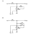
図1(A)に、入力端子からの電圧Vinの上限を制限するための、本発明のリミッタの一例を回路図で示す。101は抵抗、102はダイオード接続されたトランジスタに相当する。なお本発明で用いるトランジスタ102は、フローティングゲート(FG)とコントロールゲート(CG)の2つのゲートを有しており、ダイオード接続とは、コントロールゲートとドレイン(D)との接続を意味する。
FIG. 1A is a circuit diagram showing an example of the limiter of the present invention for limiting the upper limit of the voltage Vin from the input terminal.
また抵抗101が有する2つの端子のうち、第1の端子には入力端子から電圧Vinが供給されている。また抵抗101が有する2つの端子のうち、第2の端子には、トランジスタ102のソースまたはドレインが接続されている。具体的に図1(A)では、トランジスタ102がnチャネル型トランジスタであるので、そのコントロールゲートとドレインは、抵抗101の第2の端子に接続されており、トランジスタ102のソース(S)にはグラウンド(GND)などの一定の電圧が供給されている。逆にトランジスタ102がpチャネル型トランジスタの場合、そのソースは、抵抗101の第2の端子に接続されており、トランジスタ102のコントロールゲートとドレインにはグラウンド(GND)などの一定の電圧が供給されている。そして抵抗101が有する2つの端子のうち、第2の端子の電圧は、リミッタの出力端子の電圧Voutに相当する。
Of the two terminals of the
上記構成により、入力端子からの電圧Vinが過度に大きい場合でも、トランジスタ102で形成されるダイオードの順方向降下電圧により、出力端子の電圧Voutをリミット電圧以下に抑えることができる。このリミット電圧は、ダイオード接続されているトランジスタ102の順方向降下電圧に依存する。
With the above configuration, even when the voltage Vin from the input terminal is excessively large, the voltage Vout at the output terminal can be suppressed to a limit voltage or less by the forward voltage drop of the diode formed by the
なお本発明のリミッタは、必ずしも抵抗101を有していなくとも良い。この場合、トランジスタ102のコントロールゲートとドレインに入力端子からの電圧Vinが直接供給され、トランジスタ102によって降下したコントロールゲートとドレインの電圧が、リミッタの出力端子の電圧Voutとして、後段の回路に供給される。
Note that the limiter of the present invention does not necessarily have the
図1(B)に、トランジスタ102のドレインとソース間の電圧Vdsと、ドレイン電流Idの関係を示す。なお図1(B)では、フローティングゲートに電荷が蓄積されていない初期の状態における、電圧Vdsとドレイン電流Idの関係を、グラフ103に示す。また、フローティングゲートに電荷が蓄積されている補正後の状態における、電圧Vdsとドレイン電流Idの関係を、グラフ104に示す。なお、Vf1は初期の状態におけるトランジスタ102の順方向降下電圧、Vf2は補正後の状態におけるトランジスタ102の順方向降下電圧とする。
FIG. 1B shows the relationship between the drain-source voltage Vds of the
順方向降下電圧は、トランジスタ102の閾値電圧Vthに依存する。本発明では、フローティングゲートへの電荷の蓄積により、トランジスタ102の閾値電圧をシフトさせ、グラフ103、グラフ104に示すように、順方向降下電圧をVf1からVf2へと大きくすることができる。また本発明では、フローティングゲートへの電荷の蓄積により、逆に、順方向降下電圧を小さくすることもできる。
The forward voltage drop depends on the threshold voltage Vth of the
フローティングゲートに蓄積される電荷量は、コントロールゲートとソースの間の電圧(ゲート電圧)により制御することができる。図2を用いて、ゲート電圧と電荷量の関係について説明する。 The amount of charge accumulated in the floating gate can be controlled by the voltage (gate voltage) between the control gate and the source. The relationship between the gate voltage and the charge amount will be described with reference to FIG.
図2(A)に、閾値電圧Vthをプラス側に補正する際の、トランジスタ102の回路図を示す。Vcgはコントロールゲートに与えられる電圧、Vsはソースに与えられる電圧に相当する。図2(A)では、ホットエレクトロン注入またはトンネル電流によって、フローティングゲートに負の電荷を蓄積することができる程度に、電圧Vcgと電圧Vsの間に差を設ける。ホットエレクトロン注入またはトンネル電流によって負の電荷を蓄積することができるゲート電圧をVweと仮定した場合、Vcg−Vs≧Vweとなるように、電圧Vcgと電圧Vsとを設定すれば良い。図2(A)では、例えば電圧Vcg=12V、電圧Vs=0Vとする。
FIG. 2A shows a circuit diagram of the
図2(A)に示すようにホットエレクトロン注入またはトンネル電流によって、トランジスタ102のフローティングゲートに負の電荷が蓄積され、結果的にトランジスタ102の閾値電圧をプラス側にシフトさせることができる。
As shown in FIG. 2A, negative charge is accumulated in the floating gate of the
なお、補正前におけるトランジスタ102の閾値電圧の値が不明であったり、ホットエレクトロン注入またはトンネル電流により閾値電圧がどの程度シフトしたかを正確に把握しきれなかったりする場合、補正後の閾値電圧を読み出し、その値が目的とする範囲に収まっているかどうかを確認することができる。
Note that when the threshold voltage value of the
図2(B)に、補正された閾値電圧Vthの値、或いはリミット電圧の値を読み出す際の、トランジスタ102の回路図を示す。図2(B)では、フローティングゲートに蓄積された電荷量に変動が生じない範囲内において、電圧Vcgと電圧Vsの間の差を変化させる。トランジスタ102は、Vcg−Vsが補正後の閾値電圧と同じか、それ以上の場合にオンになるので、Vcg−Vsの値を変えながら、その都度トランジスタ102のドレイン電流を測定することで、補正後の閾値電圧が目的とする範囲に収まっているか否かを確認することができる。
FIG. 2B is a circuit diagram of the
トンネル電流によりフローティングゲートに蓄積されている負の電荷を引き抜くことができるゲート電圧をVwhと仮定した場合、具体的には、Vwh<(Vcg−Vs)<Vweを満たす範囲内において、電圧Vcgと電圧Vsとを設定すれば良い。図2(B)では、例えば電圧Vcg=0V〜8V、電圧Vs=0Vとする。 Assuming that the gate voltage that can extract the negative charge accumulated in the floating gate by the tunnel current is Vwh, specifically, the voltage Vcg is within the range satisfying Vwh <(Vcg−Vs) <Vwe. The voltage Vs may be set. In FIG. 2B, for example, the voltage Vcg = 0V to 8V and the voltage Vs = 0V.
補正後の閾値電圧が目的とする範囲よりもマイナス側の値であったならば、図2(A)に示した動作を再び行なうことで、閾値電圧をプラス側にシフトさせ、目的とする範囲に収めることができる。逆に、補正後の閾値電圧が目的とする範囲よりもプラス側の値であった場合、トンネル電流によりフローティングゲートに蓄積されている負の電荷を引き抜くことで、閾値電圧をマイナス側にシフトさせ、目的とする範囲に収めることができる。 If the corrected threshold voltage is a negative value with respect to the target range, the threshold voltage is shifted to the positive side by performing the operation shown in FIG. Can fit in. Conversely, if the corrected threshold voltage is a positive value from the target range, the threshold voltage is shifted to the negative side by extracting the negative charge accumulated in the floating gate by the tunnel current. , Can be within the intended range.
図2(C)に、閾値電圧Vthをマイナス側に補正する際の、トランジスタ102の回路図を示す。図2(C)では、トンネル電流によりフローティングゲートに蓄積されている負の電荷を引き抜くことができる程度に、電圧Vcgと電圧Vsの間に差を設ける。具体的には、Vcg−Vs≦Vwhとなるように、電圧Vcgと電圧Vsとを設定すれば良い。図2(C)では、例えば電圧Vcg=−15V、電圧Vs=0Vとする。
FIG. 2C shows a circuit diagram of the
図2(C)に示すようにフローティングゲートに蓄積されている負の電荷を引き抜くことで、トランジスタ102のフローティングゲートに蓄積されている負の電荷量を減らし、結果的にトランジスタ102の閾値電圧をマイナス側にシフトさせることができる。
As shown in FIG. 2C, by extracting the negative charge accumulated in the floating gate, the amount of negative charge accumulated in the floating gate of the
なお本実施の形態は、トランジスタの閾値電圧をプラス側に補正した後に、必要があれば、トランジスタの閾値電圧をマイナス側に補正する場合について説明しているが、本発明はこの構成に限定されない。例えば、図2(C)に示すように、トランジスタの閾値電圧をマイナス側にだけ補正するようにしても良い。 Note that although this embodiment describes a case where the threshold voltage of a transistor is corrected to the minus side if necessary after the threshold voltage of the transistor is corrected to the plus side, the present invention is not limited to this configuration. . For example, as shown in FIG. 2C, the threshold voltage of the transistor may be corrected only to the negative side.
また、図1、図2では、ダイオードとして用いているトランジスタがnチャネル型トランジスタである場合について示しているが、本発明はこの構成に限定されない。本発明のリミッタは、ダイオードとして用いるトランジスタがpチャネル型トランジスタであっても良い。ただしトランジスタ102がpチャネル型トランジスタの場合、Vcg−Vsが補正後の閾値電圧と同じか、それ以下の場合に、トランジスタ102をオンにすることができる点において、nチャネル型トランジスタの場合とは異なっている。
1 and 2 illustrate the case where the transistor used as the diode is an n-channel transistor, the present invention is not limited to this structure. In the limiter of the present invention, the transistor used as the diode may be a p-channel transistor. However, in the case where the
また図2(A)、図2(C)に示すようにトランジスタ102の閾値電圧を補正する場合、閾値電圧の変化量は、ゲート電圧のみならず補正する時間にも依存する。よってトランジスタ102の閾値電圧は、ゲート電圧だけではなく、補正する時間も制御しながら、補正することが望ましい。
2A and 2C, when the threshold voltage of the
また図1、図2では、リミッタにダイオード接続されたトランジスタが1つだけ設けられている例を示したが、本発明はこの構成に限定されない。本発明のリミッタは、ダイオード接続されたトランジスタが、複数直列に接続され、該複数のトランジスタのうち最も端部に接続されたトランジスタと抵抗とが接続されていても良い。この場合リミット電圧は、各トランジスタの順方向降下電圧Vfの和に相当する。 Although FIGS. 1 and 2 show an example in which the limiter has only one diode-connected transistor, the present invention is not limited to this configuration. In the limiter of the present invention, a plurality of diode-connected transistors may be connected in series, and a transistor connected to the end of the plurality of transistors may be connected to a resistor. In this case, the limit voltage corresponds to the sum of the forward drop voltage Vf of each transistor.
なお電圧Vcgと電圧Vsの制御は、トランジスタ102のコントロールゲート、ソースまたはドレインに接続された接続端子を、半導体装置に設け、該接続端子の電圧を半導体装置の外部において制御することで行なうことができる。或いは、半導体装置の内部に、トランジスタ102のコントロールゲート、ソースまたはドレインの電圧を制御するための回路を、設けるようにしても良い。
Note that the voltage Vcg and the voltage Vs can be controlled by providing a connection terminal connected to the control gate, source, or drain of the
また図1、図2では、入力端子からの電圧Vinの上限を制限するための、本発明のリミッタの一例について説明したが、本発明はこの構成に限定されない。本発明のリミッタは、入力端子からの電圧Vinの下限を制限する機能を有していても良い。ただしこの場合、nチャネル型トランジスタを用いていれば、そのソースを、抵抗が有する第2の端子に接続し、そのコントロールゲートとドレインにはVdd(Vdd>GND)などの一定の電圧を供給する。逆にpチャネル型トランジスタを用いていれば、そのコントロールゲートとドレインを、抵抗が有する第2の端子に接続し、そのソースにはVddなどの一定の電圧を供給する。 1 and 2, the example of the limiter of the present invention for limiting the upper limit of the voltage Vin from the input terminal has been described, but the present invention is not limited to this configuration. The limiter of the present invention may have a function of limiting the lower limit of the voltage Vin from the input terminal. However, in this case, if an n-channel transistor is used, its source is connected to the second terminal of the resistor, and a constant voltage such as Vdd (Vdd> GND) is supplied to its control gate and drain. . Conversely, if a p-channel transistor is used, its control gate and drain are connected to the second terminal of the resistor, and a constant voltage such as Vdd is supplied to its source.
そして入力端子からの電圧Vinの下限を制限するリミッタの場合も、補正と読み出しの動作時における電圧Vcg、電圧Vsと電圧Vwe、電圧Vwhの関係は、図2の場合と同様に設定すれば良い。 Also in the case of the limiter that limits the lower limit of the voltage Vin from the input terminal, the relationship between the voltage Vcg and the voltage Vs and the voltage Vwe and the voltage Vwh at the time of the correction and reading operations may be set similarly to the case of FIG. .
なお、図2に示した補正と読み出しの操作は、半導体装置が完成した後に行なうことができる。図21に、半導体装置が完成した後に行なわれる、リミット電圧の補正と読み出しの操作手順を、フローチャートで示す。 Note that the correction and readout operations shown in FIG. 2 can be performed after the semiconductor device is completed. FIG. 21 is a flowchart showing a limit voltage correction and read operation procedure performed after the semiconductor device is completed.
まず図21において、2101に示すように半導体装置が完成したら、2103に示すようにリミット電圧を読み出す。そして読み出したリミット電圧が許容範囲に収まっている場合、該半導体装置は合格と判断され、2104に示す良品に分類される。逆に、読み出したリミット電圧が許容範囲に収まっていない場合、該半導体装置は不合格と判断され、2105に示すように、フローティングゲートの電荷量の制御により、リミット電圧の補正が行なわれる。 First, in FIG. 21, when the semiconductor device is completed as indicated by 2101, the limit voltage is read as indicated by 2103. If the read limit voltage is within the allowable range, the semiconductor device is determined to be acceptable and classified as a non-defective product indicated by 2104. Conversely, if the read limit voltage is not within the allowable range, the semiconductor device is determined to be unacceptable, and the limit voltage is corrected by controlling the charge amount of the floating gate, as indicated by 2105.
そして、リミット電圧の補正が行なわれた後、2107に示すようにリミット電圧を読み出す。そして読み出したリミット電圧が許容範囲に収まっている場合、該半導体装置は合格と判断され、2104に示す良品に分類される。逆に、読み出したリミット電圧が許容範囲に収まっていない場合、該半導体装置は不合格と判断される。 After the limit voltage is corrected, the limit voltage is read as indicated by 2107. If the read limit voltage is within the allowable range, the semiconductor device is determined to be acceptable and classified as a non-defective product indicated by 2104. Conversely, when the read limit voltage is not within the allowable range, the semiconductor device is determined to be unacceptable.
そして不合格と判断された半導体装置は、2108に示すように、再びフローティングゲートの電荷量の制御により、リミット電圧の補正が行なわれる。なお、上記操作を繰り返しても半導体装置が不合格である場合、2109に示すように、該半導体装置は不良品に分類される。
Then, as shown by
上記動作を繰り返すことで、歩留まりを高めることが可能である。なお、図21では、フローティングゲートの電荷量の制御を、2105、2108に示すように2回行なっているが、1回で済ませても良いし、3回以上行なっても良い。 The yield can be increased by repeating the above operation. In FIG. 21, the control of the charge amount of the floating gate is performed twice as indicated by 2105 and 2108. However, it may be performed once or three times or more.
次に、上述したリミッタを集積回路に用いている、本発明の半導体装置について説明する。 Next, a semiconductor device of the present invention using the above-described limiter for an integrated circuit will be described.
図3(A)に、本発明の半導体装置の一つであるIDチップの一形態を、斜視図で示す。201は集積回路、202はアンテナに相当し、アンテナ202は集積回路201に接続されている。203は基板、204はカバー材に相当する。集積回路201及びアンテナ202は、基板203上に形成されており、カバー材204は集積回路201及びアンテナ202を覆うように基板203と重なっている。なおカバー材204は必ずしも用いる必要はないが、集積回路201及びアンテナ202をカバー材204で覆うことで、IDチップの機械的強度を高めることができる。
FIG. 3A is a perspective view showing one mode of an ID chip which is one of the semiconductor devices of the present invention.
図3(B)に、本発明の半導体装置の一つであるICカードの一形態を、斜視図で示す。205は集積回路、206はアンテナに相当し、アンテナ206は集積回路205に接続されている。208はインレットシートとして機能する基板、207、209はカバー材に相当する。集積回路205及びアンテナ206は基板208上に形成されており、基板208は2つのカバー材207、209の間に挟まれている。なお本発明のICカードは、集積回路205に接続された表示装置を有していても良い。
FIG. 3B is a perspective view showing one mode of an IC card which is one of the semiconductor devices of the present invention.
次に、本発明の半導体装置が有する集積回路の、具体的な構成について説明する。図4(A)に、本発明の半導体装置の、機能的な構成の一形態をブロック図で示す。 Next, a specific structure of the integrated circuit included in the semiconductor device of the present invention will be described. FIG. 4A is a block diagram illustrating one mode of a functional structure of the semiconductor device of the present invention.
図4(A)において、301は集積回路、302はアンテナに相当する。集積回路301は、整流回路303、クロック生成回路304、変調回路306、復調回路305、リミッタ307、論理回路部308とを有している。論理回路部308には各種演算回路、メモリなどが含まれていても良い。メモリには、例えばSRAM、フラッシュメモリ、ROMまたはFeRAM(Ferroelectric RAM)などを用いることができる。
In FIG. 4A, 301 corresponds to an integrated circuit, and 302 corresponds to an antenna. The
リーダ/ライタから電波として送られてきた信号は、アンテナ302において電磁誘導により交流電圧に変換される。復調回路305では該交流電圧を復調して信号を生成し、後段の論理回路部308に入力する。また整流回路303では、交流電圧を用いて電源電圧を生成する。該電源電圧は、整流回路303の後段に設けられたリミッタ307においてリミット電圧以下に補正された後、論理回路部308に供給される。
A signal transmitted as a radio wave from the reader / writer is converted into an AC voltage by electromagnetic induction in the
論理回路部308では、復調回路305から入力された信号、リミッタ307から供給された電源電圧を用いて、動作を行なう。そして論理回路部308が動作することで、論理回路部308から変調回路306に信号が送られる。変調回路306は論理回路部308からの信号に従って、アンテナ302に負荷変調を加えることができる。リーダ/ライタは、アンテナ302に加えられた負荷変調を電波で受け取ることで、結果的に論理回路部308からの信号を受信することができる。
The
なお図4(A)では、リミッタ307を整流回路303の後段に設けているが、本発明はこの構成に限定されない。リミッタ307は整流回路303の前段に設けても良い。或いは、クロック生成回路304の前段または後段、変調回路306の前段または後段、復調回路305の前段または後段、論理回路部308の内部などに設けていても良い。
In FIG. 4A, the
図4(B)に、リミッタ307を整流回路303の前段に設けた場合の、本発明の半導体装置の、機能的な構成の一形態をブロック図で示す。なお図4(B)では、図4(A)において既に示したものに対し、同じ符号を付している。図4(B)の場合、アンテナ302からの交流電圧を、リミッタ307においてリミット電圧以下に補正している。そして整流回路303ではリミット電圧以下に補正された交流電圧を用いて、電源電圧を生成している。
FIG. 4B is a block diagram illustrating one mode of a functional configuration of the semiconductor device of the present invention in the case where the
なお本発明の半導体装置における信号の伝送方式は、電磁結合方式、電磁誘導方式、マイクロ波方式やその他の伝送方式を用いることができる。特に、電磁結合方式や電磁誘導方式の場合、強い電波に半導体装置がさらされることで、アンテナに過度に大きい交流電圧が生じてしまう恐れがある。またマイクロ波方式やその他の伝送方式であっても、半導体装置内で信号のノイズが生じる場合がある。本発明のリミッタを設けることは、過度に大きい交流電圧や信号のノイズによって、集積回路において絶縁破壊が生じるのを防止することができ、非常に有効である。 Note that as a signal transmission method in the semiconductor device of the present invention, an electromagnetic coupling method, an electromagnetic induction method, a microwave method, and other transmission methods can be used. In particular, in the case of the electromagnetic coupling method or the electromagnetic induction method, an excessively large AC voltage may be generated in the antenna when the semiconductor device is exposed to strong radio waves. Even in the microwave system or other transmission systems, signal noise may occur in the semiconductor device. Providing the limiter of the present invention is very effective because it can prevent dielectric breakdown from occurring in an integrated circuit due to excessively large AC voltage or signal noise.
また本実施の形態では、アンテナが円状または螺旋状に巻かれた導線を有している場合について説明したが、本発明はこの構成に限定されない。導電体で形成された膜(導電膜)をアンテナとして用いていても良い。 In this embodiment mode, the case where the antenna has a conducting wire wound in a circular shape or a spiral shape has been described, but the present invention is not limited to this configuration. A film (conductive film) formed of a conductor may be used as an antenna.
本実施例では、複数のダイオード接続されたトランジスタを用いた、本発明のリミッタについて説明する。 In this embodiment, a limiter of the present invention using a plurality of diode-connected transistors will be described.
図5(A)に、本実施例のリミッタの回路図を示す。図5(A)において、401は抵抗、402、403はダイオード接続されたトランジスタに相当する。トランジスタ402、403は、それぞれフローティングゲート(FG)とコントロールゲート(CG)の2つのゲートを有している。図5(A)では、トランジスタ402とトランジスタ403がnチャネル型トランジスタの場合を示しているが、どちらか一方がpチャネル型トランジスタ、或いは両方がpチャネル型トランジスタであっても良い。ただしダイオード接続された全てのトランジスタは、順方向電流の向きが同じになるように、直列に接続する。
FIG. 5A shows a circuit diagram of the limiter of this embodiment. In FIG. 5A, 401 corresponds to a resistor, and 402 and 403 correspond to diode-connected transistors. The
抵抗401が有する2つの端子のうち、第1の端子には入力端子からの電圧Vinが供給されている。また、トランジスタ402とトランジスタ403は、順方向電流の向きが同じになるように、直列に接続されている。図5(A)の場合、具体的には、トランジスタ402のコントロールゲートとドレイン(D)が、抵抗401の第2の端子に接続され、トランジスタ403のコントロールゲートとドレインが、トランジスタ402のソース(S)に接続され、トランジスタ403のソースにはグラウンド(GND)などの一定の電圧が供給されている。そして抵抗401が有する2つの端子のうち、第2の端子の電圧は、リミッタの出力端子の電圧Voutに相当する。
Of the two terminals of the
図5(A)のように、複数のダイオード接続されたトランジスタを、直列に接続して用いる場合、リミット電圧は各トランジスタの順方向降下電圧Vfの和に相当する。 When a plurality of diode-connected transistors are used in series as shown in FIG. 5A, the limit voltage corresponds to the sum of the forward drop voltages Vf of the transistors.
なお図5(A)に示すリミッタは、必ずしも抵抗401を有していなくとも良い。この場合、トランジスタ402のコントロールゲートとドレインに入力端子からの電圧Vinが直接供給され、トランジスタ402によって降下したコントロールゲートとドレインの電圧が、リミッタの出力端子の電圧Voutとして、後段の回路に供給される。
Note that the limiter illustrated in FIG. 5A does not necessarily include the
図5(B)に、図5(A)とは異なる、本実施例のリミッタの回路図を示す。図5(B)において、411は抵抗、412、413はダイオード接続されたトランジスタに相当する。トランジスタ412は、フローティングゲートを有しておらず、ゲート(G)のみを有している。トランジスタ413は、フローティングゲート(FG)とコントロールゲート(CG)の2つのゲートを有している。図5(B)では、トランジスタ412とトランジスタ413がnチャネル型トランジスタの場合を示しているが、どちらか一方がpチャネル型トランジスタ、或いは両方がpチャネル型トランジスタであっても良い。ただしダイオード接続された全てのトランジスタは、順方向電流の向きが同じになるように、直列に接続する。
FIG. 5B shows a circuit diagram of the limiter of this embodiment, which is different from FIG. In FIG. 5B, 411 corresponds to a resistor, and 412 and 413 correspond to diode-connected transistors. The
抵抗411が有する2つの端子のうち、第1の端子には入力端子からの電圧Vinが供給されている。また、トランジスタ412とトランジスタ413は、順方向電流の向きが同じになるように、直列に接続されている。図5(B)の場合、具体的には、トランジスタ412のゲートとドレイン(D)が、抵抗411の第2の端子に接続され、トランジスタ413のコントロールゲートとドレインが、トランジスタ412のソース(S)に接続され、トランジスタ413のソースにはグラウンド(GND)などの一定の電圧が供給されている。そして抵抗411が有する2つの端子のうち、第2の端子の電圧は、リミッタの出力端子の電圧Voutに相当する。
Of the two terminals included in the
図5(B)に示すリミッタも、図5(A)と同様に、複数のダイオード接続されたトランジスタを、直列に接続して用いているため、リミット電圧は各トランジスタの順方向降下電圧Vfの和に相当する。 Similarly to FIG. 5A, the limiter shown in FIG. 5B uses a plurality of diode-connected transistors connected in series. Therefore, the limit voltage is the forward drop voltage Vf of each transistor. Equivalent to the sum.
なお図5(B)に示すリミッタは、必ずしも抵抗411を有していなくとも良い。この場合、トランジスタ412のゲートとドレインに入力端子からの電圧Vinが直接供給され、トランジスタ412によって降下したゲートとドレインの電圧が、リミッタの出力端子の電圧Voutとして、後段の回路に供給される。
Note that the limiter illustrated in FIG. 5B does not necessarily include the
図5(C)に、図5(A)、図5(B)とは異なる、本実施例のリミッタの回路図を示す。図5(C)において、421は抵抗、422、423はダイオード接続されたトランジスタに相当する。トランジスタ422は、フローティングゲート(FG)とコントロールゲート(CG)の2つのゲートを有している。トランジスタ423は、フローティングゲートを有しておらず、ゲート(G)のみを有している。図5(C)では、トランジスタ422とトランジスタ423がnチャネル型トランジスタの場合を示しているが、どちらか一方がpチャネル型トランジスタ、或いは両方がpチャネル型トランジスタであっても良い。ただしダイオード接続された全てのトランジスタは、順方向電流の向きが同じになるように、直列に接続する。
FIG. 5C shows a circuit diagram of the limiter of this embodiment, which is different from FIGS. 5A and 5B. In FIG. 5C, 421 corresponds to a resistor, and 422 and 423 correspond to diode-connected transistors. The
抵抗421が有する2つの端子のうち、第1の端子には入力端子からの電圧Vinが供給されている。また、トランジスタ422とトランジスタ423は、順方向電流の向きが同じになるように、直列に接続されている。図5(C)の場合、具体的には、トランジスタ422のコントロールゲートとドレイン(D)が、抵抗421の第2の端子に接続され、トランジスタ423のゲートとドレインが、トランジスタ422のソース(S)に接続され、トランジスタ423のソースにはグラウンド(GND)などの一定の電圧が供給されている。そして抵抗421が有する2つの端子のうち、第2の端子の電圧は、リミッタの出力端子の電圧Voutに相当する。
Of the two terminals of the
図5(C)に示すリミッタも、図5(A)、図5(B)と同様に、複数のダイオード接続されたトランジスタを、直列に接続して用いているため、リミット電圧は各トランジスタの順方向降下電圧Vfの和に相当する。 Similarly to FIGS. 5A and 5B, the limiter shown in FIG. 5C uses a plurality of diode-connected transistors connected in series. This corresponds to the sum of the forward voltage drop Vf.
なお図5(C)に示すリミッタは、必ずしも抵抗421を有していなくとも良い。この場合、トランジスタ422のコントロールゲートとドレインに入力端子からの電圧Vinが直接供給され、トランジスタ422によって降下したコントロールゲートとドレインの電圧が、リミッタの出力端子の電圧Voutとして、後段の回路に供給される。
Note that the limiter illustrated in FIG. 5C does not necessarily include the
なお本実施例では、入力端子からの電圧Vinの上限を制限するためのリミッタについて説明したが、電圧Vinの下限を制限するためのリミッタであっても良い。 In this embodiment, the limiter for limiting the upper limit of the voltage Vin from the input terminal has been described. However, a limiter for limiting the lower limit of the voltage Vin may be used.
また本発明では、ダイオード接続されたトランジスタの数は2つに限定されず、3つ以上のダイオード接続されたトランジスタが直列に接続されていても良い。 In the present invention, the number of diode-connected transistors is not limited to two, and three or more diode-connected transistors may be connected in series.
本実施例で示したような、ダイオード接続されたトランジスタもしくはダイオード(以下本実施例では、共にダイオードと呼ぶ)を、複数直列に接続した構成は、以下の点で好ましい。 A configuration in which a plurality of diode-connected transistors or diodes (hereinafter, both referred to as diodes in this embodiment) are connected in series as shown in this embodiment is preferable in the following points.
チップ内において、通常リミッタは、電源線と接地線を介して論理回路と並列に接続されている。しかしリミッタは、フローティングゲートに蓄積されている電荷を制御する際、ダイオードに高電圧を供給する必要があり、該高電圧は論理回路にとって過剰に高い値を有している。 In the chip, the limiter is normally connected in parallel with the logic circuit via a power supply line and a ground line. However, the limiter needs to supply a high voltage to the diode when controlling the charge accumulated in the floating gate, and the high voltage has an excessively high value for the logic circuit.
本実施例のリミッタの場合、ダイオードの一つに高電圧を印加しても、該高電圧が他のダイオードにとって逆方向電圧であるときは、実質的に論理回路へは高電圧が印加されない。また、該高電圧が他のダイオードにとって順方向電圧であっても、当該他のダイオードのしきい値だけ、論理回路に直接印加される電圧は低減される。 In the case of the limiter of this embodiment, even if a high voltage is applied to one of the diodes, if the high voltage is a reverse voltage for the other diode, the high voltage is not substantially applied to the logic circuit. Even if the high voltage is a forward voltage for another diode, the voltage directly applied to the logic circuit is reduced by the threshold value of the other diode.
このようにダイオードを複数直列に接続することで、1つのダイオードで構成されたリミッタに比べて、リミット電圧を補正する際に、論理回路への高電圧の印加を緩和することができる。 By connecting a plurality of diodes in series in this way, it is possible to reduce the application of a high voltage to the logic circuit when correcting the limit voltage, as compared to a limiter configured with one diode.
本発明では、トランジスタのコントロールゲートとドレインの間に、他の半導体素子が設けられていても、該トランジスタがダイオードとして機能するのであれば、ダイオード接続されていると見なすことができる。本実施例では、リミッタに用いられているトランジスタの、コントロールゲートとドレインの間に、他の半導体素子が設けられている例について説明する。 In the present invention, even if another semiconductor element is provided between the control gate and the drain of the transistor, it can be regarded as diode-connected as long as the transistor functions as a diode. In this embodiment, an example in which another semiconductor element is provided between a control gate and a drain of a transistor used in a limiter will be described.
図6(A)に本実施例のリミッタの一例を、回路図で示す。図6(A)において、431、433は抵抗、432はトランジスタに相当する。トランジスタ432は、フローティングゲート(FG)とコントロールゲート(CG)の2つのゲートを有している。図6(A)では、トランジスタ432がnチャネル型トランジスタの場合を示している。
FIG. 6A is a circuit diagram showing an example of the limiter of this embodiment. In FIG. 6A, 431 and 433 correspond to resistors, and 432 corresponds to a transistor. The
抵抗431が有する2つの端子のうち、第1の端子には入力端子からの電圧Vinが供給されている。またトランジスタ432のコントロールゲートとドレイン(D)の間には、抵抗433が接続されている。そしてトランジスタ432のドレインは、抵抗431が有する2つの端子のうち、第2の端子に接続されている。またトランジスタ432のソースには、グラウンド(GND)などの一定の電圧が供給されている。そして抵抗431が有する2つの端子のうち、第2の端子の電圧は、リミッタの出力端子の電圧Voutに相当する。
Of the two terminals of the
なお図6(A)では、トランジスタ432がnチャネル型トランジスタの場合を示しているが、トランジスタ432はpチャネル型トランジスタであっても良い。ただしトランジスタ432がpチャネル型トランジスタの場合でも、nチャネル型トランジスタの場合と順方向電流の向きが同じになるようにする。
Note that FIG. 6A illustrates the case where the
なお図6(A)に示すリミッタは、必ずしも抵抗431を有していなくとも良い。この場合、トランジスタ432のドレインに入力端子からの電圧Vinが直接供給され、トランジスタ432によって降下したドレインの電圧が、リミッタの出力端子の電圧Voutとして、後段の回路に供給される。
Note that the limiter illustrated in FIG. 6A does not necessarily include the
図6(B)に本実施例のリミッタの一例を、回路図で示す。図6(B)において、441は抵抗、442はトランジスタ、443、444はダイオードに相当する。トランジスタ442は、フローティングゲート(FG)とコントロールゲート(CG)の2つのゲートを有している。図6(B)では、トランジスタ442がnチャネル型トランジスタの場合を示している。 FIG. 6B is a circuit diagram showing an example of the limiter of this embodiment. In FIG. 6B, 441 corresponds to a resistor, 442 corresponds to a transistor, and 443 and 444 correspond to diodes. The transistor 442 has two gates, a floating gate (FG) and a control gate (CG). FIG. 6B illustrates the case where the transistor 442 is an n-channel transistor.
抵抗441が有する2つの端子のうち、第1の端子には入力端子からの電圧Vinが供給されている。またトランジスタ442のコントロールゲートとドレイン(D)の間には、ダイオード443とダイオード444が並列に接続されている。そして、ダイオード443とダイオード444は、順方向電流の向きが互いに逆になるように、接続されている。またトランジスタ442のドレインは、抵抗441が有する2つの端子のうち、第2の端子に接続されている。トランジスタ442のソースには、グラウンド(GND)などの一定の電圧が供給されている。そして抵抗441が有する2つの端子のうち、第2の端子の電圧は、リミッタの出力端子の電圧Voutに相当する。
Of the two terminals included in the
なお図6(B)では、トランジスタ442がnチャネル型トランジスタの場合を示しているが、トランジスタ442はpチャネル型トランジスタであっても良い。ただしトランジスタ442がpチャネル型トランジスタの場合でも、nチャネル型トランジスタの場合と順方向電流の向きが同じになるようにする。 Note that FIG. 6B illustrates the case where the transistor 442 is an n-channel transistor; however, the transistor 442 may be a p-channel transistor. However, even when the transistor 442 is a p-channel transistor, the direction of the forward current is made to be the same as that of the n-channel transistor.
なお図6(B)に示すリミッタは、必ずしも抵抗441を有していなくとも良い。この場合、トランジスタ442のドレインに入力端子からの電圧Vinが直接供給され、トランジスタ442によって降下したドレインの電圧が、リミッタの出力端子の電圧Voutとして、後段の回路に供給される。
Note that the limiter illustrated in FIG. 6B does not necessarily include the
なお本実施例では、入力端子からの電圧Vinの上限を制限するためのリミッタについて説明したが、電圧Vinの下限を制限するためのリミッタであっても良い。本実施例のリミッタは、実施の形態、実施例1に示したリミッタのいずれの構成を有していてもよい。 In this embodiment, the limiter for limiting the upper limit of the voltage Vin from the input terminal has been described. However, a limiter for limiting the lower limit of the voltage Vin may be used. The limiter of this example may have any of the configurations of the embodiment and the limiter shown in Example 1.
本実施例では、オペアンプを用いた本発明のリミッタについて説明する。 In this embodiment, a limiter of the present invention using an operational amplifier will be described.
図7に本実施例のリミッタの一例を、回路図で示す。図7において、451は抵抗、452はダイオード接続されたトランジスタ、453はオペアンプに相当する。トランジスタ452は、フローティングゲート(FG)とコントロールゲート(CG)の2つのゲートを有している。なお図7では、トランジスタ452がnチャネル型トランジスタの場合を示している。
FIG. 7 is a circuit diagram showing an example of the limiter of this embodiment. In FIG. 7, 451 corresponds to a resistor, 452 corresponds to a diode-connected transistor, and 453 corresponds to an operational amplifier. The
抵抗451が有する2つの端子のうち、第1の端子には入力端子からの電圧Vinが供給されている。またトランジスタ452のコントロールゲートとドレイン(D)は、抵抗451が有する2つの端子のうち、第2の端子に接続されている。トランジスタ452のソース(S)には、グラウンド(GND)などの一定の電圧が供給されている。
Of the two terminals of the
また抵抗451の第2の端子は、オペアンプ453の非反転入力端子に接続されている。オペアンプ453の反転入力端子は出力端子に接続されており、該出力端子の電圧は、リミッタの出力端子の電圧Voutに相当する。
The second terminal of the
本実施例のように、リミッタの出力側にオペアンプなどのアナログバッファを設けることで、出力インピーダンスを抑えることができる。なお本実施例では、アナログバッファとしてオペアンプを用いた例を示しているが、オペアンプ以外のアナログバッファも同様に用いることができる。 By providing an analog buffer such as an operational amplifier on the output side of the limiter as in this embodiment, the output impedance can be suppressed. In this embodiment, an example in which an operational amplifier is used as an analog buffer is shown, but an analog buffer other than the operational amplifier can be used similarly.
なお図7では、トランジスタ452がnチャネル型トランジスタの場合を示しているが、トランジスタ452はpチャネル型トランジスタであっても良い。ただしトランジスタ452がpチャネル型トランジスタの場合でも、nチャネル型トランジスタの場合と順方向電流の向きが同じになるようにする。
Note that FIG. 7 illustrates the case where the
なお図7に示すリミッタは、必ずしも抵抗451を有していなくとも良い。この場合、トランジスタ452のコントロールゲートとドレインに入力端子からの電圧Vinが直接供給され、トランジスタ452によって降下したコントロールゲートとドレインの電圧が、オペアンプ453の非反転入力端子に供給される。
Note that the limiter illustrated in FIG. 7 does not necessarily include the
なお本実施例では、入力端子からの電圧Vinの上限を制限するためのリミッタについて説明したが、電圧Vinの下限を制限するためのリミッタであっても良い。また、本実施例のリミッタは、実施の形態、実施例1及び実施例2に示したリミッタのいずれの構成を有していてもよい。 In this embodiment, the limiter for limiting the upper limit of the voltage Vin from the input terminal has been described. However, a limiter for limiting the lower limit of the voltage Vin may be used. Further, the limiter of the present embodiment may have any of the configurations of the limiters shown in the embodiment, the first embodiment, and the second embodiment.
本実施例では、フローティングゲートの電荷量を制御するための制御回路を、リミッタと共に半導体装置内に設ける例について説明する。 In this embodiment, an example in which a control circuit for controlling the charge amount of a floating gate is provided in a semiconductor device together with a limiter will be described.
図8に、リミッタ460と、制御回路に相当するパルス生成回路463及び昇圧回路464のブロック図を示す。なお図8では、リミッタ460が、実施例1に示した図5(B)と同じ構成を有している例を示しているが、本実施例はこの構成に限定されない。本実施例のリミッタ460は、実施の形態、実施例1〜実施例3に示したリミッタのいずれの構成を有していても良い。
FIG. 8 shows a block diagram of a
図8においてリミッタ460は、抵抗465、ダイオード接続されたトランジスタ466、467を有している。トランジスタ467は、フローティングゲートを有しておらず、ゲート(G)のみを有している。トランジスタ466は、フローティングゲート(FG)とコントロールゲート(CG)の2つのゲートを有している。図8では、トランジスタ467とトランジスタ466がnチャネル型トランジスタの場合を示しているが、どちらか一方がpチャネル型トランジスタ、或いは両方がpチャネル型トランジスタであっても良い。
In FIG. 8, the
抵抗465が有する2つの端子のうち、第1の端子には入力端子からの電圧Vinが供給されている。また、トランジスタ467とトランジスタ466は、順方向電流の向きが同じになるように、直列に接続されている。図8の場合、具体的には、トランジスタ467のゲートとドレイン(D)が、抵抗465の第2の端子に接続され、トランジスタ466のドレインがトランジスタ467のソース(S)に接続され、トランジスタ466のソースにはグラウンド(GND)などの一定の電圧が供給されている。そして抵抗465が有する2つの端子のうち、第2の端子の電圧は、リミッタの出力端子の電圧Voutに相当する。
Of the two terminals included in the
図8に示すリミッタは、複数のダイオード接続されたトランジスタを、直列に接続して用いているため、リミット電圧は各トランジスタの順方向降下電圧Vfの和に相当する。 Since the limiter shown in FIG. 8 uses a plurality of diode-connected transistors connected in series, the limit voltage corresponds to the sum of the forward drop voltages Vf of the transistors.
なお本実施例のリミッタでは、トランジスタ466のコントロールゲートを、トランジスタ466のドレインに接続するのではなく、パルス生成回路463に接続する。またトランジスタ466のドレインとソースも、それぞれパルス生成回路463に接続する。
In the limiter of this embodiment, the control gate of the
昇圧回路464は、トランジスタ466の閾値電圧の補正時に用いられる電圧Vcg、電圧Vd、電圧Vsを生成し、パルス生成回路463に供給する。パルス生成回路463は、動作に合わせて適切な電圧を選択して、パルス幅が制御された信号を生成し、トランジスタ466のコントロールゲート、ソース、ドレインの各端子に、該信号の電圧を印加する。
The
本実施例では、半導体装置の外部において接続端子を介してトランジスタ466のコントロールゲート、ドレイン及びソースの電圧を制御するのではなく、半導体装置の内部においてパルス生成回路463を用いて制御する。
In this embodiment, the voltage of the control gate, drain, and source of the
次に図8に示したリミッタ460の、具体的な動作について説明する。IDチップの通常の動作時には、本来の機能を果たすようにリミッタ460を動作させる。つまり、パルス生成回路463を用いて、トランジスタ466のドレインとコントロールゲートを接続し、また、トランジスタ466のソースをハイインピーダンス状態にする。
Next, a specific operation of the
そしてリミット電圧の読み出しは、リーダ/ライタからの出力振幅や周波数を変化させて、IDチップの応答を見ることで行なうことができる。 The limit voltage can be read by changing the output amplitude and frequency from the reader / writer and looking at the response of the ID chip.
具体的に、リミット電圧が低い場合、IDチップ内に十分な電源電圧が得られず、IDチップの周波数特性が仕様を満たさなくなる。よって、例えばリーダ/ライタの出力や通信距離を仕様値に設定しても、IDチップの周波数特性が仕様を満たさない場合には、リミット電圧が低いと判断することができる。この場合、リミット電圧が高まるように、トランジスタ466の閾値電圧を補正すれば良い。
Specifically, when the limit voltage is low, a sufficient power supply voltage cannot be obtained in the ID chip, and the frequency characteristics of the ID chip do not satisfy the specifications. Therefore, for example, even if the output of the reader / writer and the communication distance are set to specification values, if the frequency characteristics of the ID chip do not satisfy the specifications, it can be determined that the limit voltage is low. In this case, the threshold voltage of the
逆にリミット電圧が高い場合、IDチップ内に過剰な電源電圧が発生して、場合によっては集積回路が破壊される恐れが有る。よって、例えばリーダ/ライタからの出力振幅や通信距離を仕様値に設定して、IDチップの周波数特性が仕様を十分満たす場合には、リミット電圧が高いと判断することができる。この場合、動作マージンを確保したうえでリミット電圧が低くなるように、トランジスタ466の閾値電圧を補正すれば良い。
On the other hand, when the limit voltage is high, an excessive power supply voltage is generated in the ID chip, and in some cases, the integrated circuit may be destroyed. Therefore, for example, when the output amplitude or communication distance from the reader / writer is set to a specification value and the frequency characteristics of the ID chip sufficiently satisfy the specification, it can be determined that the limit voltage is high. In this case, the threshold voltage of the
そして、トランジスタ466の閾値電圧の補正は、リーダ/ライタからの補正命令に基づいて行なう。
Then, the threshold voltage of the
閾値電圧を高めるための補正は、例えばVd=Vcg=12V、Vs=0Vの短いパルス(例えば、1μs〜10μs)をトランジスタ466に印加して、ホットエレクトロン注入またはトンネル電流により行なうことができる。逆に閾値電圧を低くするための補正は、例えばVcg=−15V、Vd=Vs=0Vの短いパルス(例えば、100μs〜1ms)をトランジスタ466に印加して、トンネル電流により行なうことができる。
Correction for increasing the threshold voltage can be performed by applying a short pulse (eg, 1 μs to 10 μs) of Vd = Vcg = 12 V and Vs = 0 V to the
なお閾値電圧の補正は、リミッタ460に順方向電流を流さないように、IDチップ内部の電源電圧がリミット電圧以下となるような環境で行なう必要が有る。
It is necessary to correct the threshold voltage in an environment in which the power supply voltage inside the ID chip is equal to or lower than the limit voltage so that forward current does not flow through the
以上のように、制御回路をIDチップ内部に設けることで、リーダ/ライタを用いたリミット電圧の設定を行なうことができる。よって、例えば出荷後に、ユーザがリミット電圧の設定を変更することも可能となる。 As described above, by providing the control circuit inside the ID chip, it is possible to set a limit voltage using a reader / writer. Therefore, for example, the user can change the setting of the limit voltage after shipment.
また本実施例のように、制御回路をリミッタと共に半導体装置内に設けることで、半導体装置に設けられる接続端子の数を減少させることができる。 Further, by providing the control circuit in the semiconductor device together with the limiter as in this embodiment, the number of connection terminals provided in the semiconductor device can be reduced.
なお図8に示すリミッタは、必ずしも抵抗465を有していなくとも良い。この場合、トランジスタ467のゲートとドレインに入力端子からの電圧Vinが直接供給され、トランジスタ467によって降下したゲートとドレインの電圧が、リミッタの出力端子の電圧Voutとして、後段の回路に供給される。
Note that the limiter illustrated in FIG. 8 does not necessarily have the
なお本実施例では、入力端子からの電圧Vinの上限を制限するためのリミッタについて説明したが、電圧Vinの下限を制限するためのリミッタであっても良い。 In this embodiment, the limiter for limiting the upper limit of the voltage Vin from the input terminal has been described. However, a limiter for limiting the lower limit of the voltage Vin may be used.
次に、本発明の半導体装置の1つである、IDチップの詳しい作製方法について説明する。なお本実施例では、TFTを半導体素子の一例として示すが、集積回路に用いられる半導体素子はこれに限定されない。例えばTFTの他に、記憶素子、ダイオード、光電変換素子、抵抗素子などを用いることができる。また、その他の素子として、コイル、容量素子、インダクタなどを用いることができる。 Next, a detailed method for manufacturing an ID chip, which is one of the semiconductor devices of the present invention, will be described. Note that in this embodiment, a TFT is shown as an example of a semiconductor element; however, a semiconductor element used for an integrated circuit is not limited to this. For example, a memory element, a diode, a photoelectric conversion element, a resistance element, or the like can be used in addition to the TFT. As other elements, a coil, a capacitive element, an inductor, or the like can be used.
まず図9(A)に示すように、耐熱性を有する第1の基板500上に剥離層501を形成する。第1の基板500として、例えばバリウムホウケイ酸ガラスや、アルミノホウケイ酸ガラスなどのガラス基板、石英基板、セラミック基板等を用いることができる。また、ステンレス基板を含む金属基板または半導体基板を用いても良い。プラスチック等の可撓性を有する合成樹脂からなる基板は、一般的に上記基板と比較して耐熱温度が低い傾向にあるが、作製工程における処理温度に耐え得るのであれば用いることが可能である。
First, as illustrated in FIG. 9A, a
剥離層501は、非晶質珪素、多結晶珪素、単結晶珪素、微結晶珪素(セミアモルファスシリコンを含む)等、珪素を主成分とする層を用いることができる。剥離層501は、スパッタ法、減圧CVD法、プラズマCVD法等を用いて形成することができる。本実施例では、膜厚50nm程度の非晶質珪素をプラズマCVD法で形成し、剥離層501として用いる。剥離層501は、スパッタ法で形成するよりもプラズマCVD法を用いて形成する方が、剥離層501に塵埃が含まれてしまうのを防ぐことができ、また剥離層501に含まれるArの量を抑えることができる。従って、後の作製工程においてレーザ結晶化などを含む熱処理が剥離層501に加えられても、塵埃やAr起因により、剥離層501が後に形成される下地膜502から剥離するのを抑えることができる。なお剥離層501は珪素に限定されず、エッチングにより選択的に除去できる材料で形成すれば良い。剥離層501の膜厚は、10〜100nmとするのが望ましい。
The
次に、剥離層501上に、下地膜502を形成する。下地膜502は第1の基板500中に含まれるNaなどのアルカリ金属やアルカリ土類金属が、半導体膜中に拡散し、TFTなどの半導体素子の特性に悪影響を及ぼすのを防ぐために設ける。また下地膜502は、後の半導体素子を剥離する工程において、半導体素子を保護する役目も有している。下地膜502には、例えば酸化珪素、酸化窒化珪素、窒化珪素、窒化酸化珪素などの絶縁膜を用いることができる。
Next, a
下地膜502は、単数の絶縁膜を用いたものであっても、複数の絶縁膜を積層して用いたものであっても良い。本実施例では、膜厚100nmの酸化窒化珪素膜、膜厚50nmの窒化酸化珪素膜、膜厚100nmの酸化窒化珪素膜を順に積層して下地膜502を形成するが、各膜の材質、膜厚、積層数は、これに限定されるものではない。例えば、下層の酸化窒化珪素膜に代えて、膜厚0.5〜3μmのシロキサン系樹脂をスピンコート法、スリットコーター法、液滴吐出法、印刷法などによって形成しても良い。また、中層の窒化酸化珪素膜に代えて、窒化珪素膜(SiNx、Si3N4等)を用いてもよい。また、上層の酸化窒化珪素膜に代えて、酸化珪素膜を用いていても良い。また、それぞれの膜厚は、0.05〜3μmとするのが望ましく、その範囲から自由に選択することができる。
The
或いは、剥離層501に最も近い、下地膜502の下層を酸化窒化珪素膜または酸化珪素膜で形成し、中層をシロキサン系樹脂で形成し、上層を酸化珪素膜で形成しても良い。
Alternatively, the lower layer of the
なおシロキサン系樹脂とは、Si−O−Si結合を含む樹脂に相当する。シロキサンは、シリコン(Si)と酸素(O)との結合で骨格構造が構成される。置換基として、少なくとも水素を含む有機基(例えばアルキル基、芳香族炭化水素)が用いられる。置換基として、フルオロ基を用いてもよい。または置換基として、少なくとも水素を含む有機基と、フルオロ基とを用いてもよい。 Note that the siloxane-based resin corresponds to a resin including a Si—O—Si bond. Siloxane has a skeleton structure formed of a bond of silicon (Si) and oxygen (O). As a substituent, an organic group containing at least hydrogen (for example, an alkyl group or an aromatic hydrocarbon) is used. A fluoro group may be used as a substituent. Alternatively, an organic group containing at least hydrogen and a fluoro group may be used as a substituent.
酸化珪素膜は、SiH4とO2、TEOS(テトラエトキシシラン)とO2等の混合ガスを用い、熱CVD、プラズマCVD、常圧CVD、バイアスECRCVD等の方法によって形成することができる。また、窒化珪素膜は、代表的には、SiH4とNH3の混合ガスを用い、プラズマCVDによって形成することができる。また、酸化窒化珪素膜、窒化酸化珪素膜は、代表的には、SiH4とN2Oの混合ガスを用い、プラズマCVDによって形成することができる。 The silicon oxide film can be formed by a method such as thermal CVD, plasma CVD, atmospheric pressure CVD, or bias ECRCVD using a mixed gas such as SiH 4 and O 2 , TEOS (tetraethoxysilane) and O 2 . The silicon nitride film can be typically formed by plasma CVD using a mixed gas of SiH 4 and NH 3 . The silicon oxynitride film and the silicon nitride oxide film can be typically formed by plasma CVD using a mixed gas of SiH 4 and N 2 O.
次に、下地膜502上に半導体膜503を形成する。半導体膜503は、下地膜502を形成した後、大気に曝さずに形成することが望ましい。半導体膜503の膜厚は20〜200nm(望ましくは40〜170nm、好ましくは50〜150nm)とする。なお半導体膜503は、非晶質半導体であっても良いし、セミアモルファス半導体であっても良いし、多結晶半導体であっても良い。また半導体は珪素だけではなくシリコンゲルマニウムも用いることができる。シリコンゲルマニウムを用いる場合、ゲルマニウムの濃度は0.01〜4.5atomic%程度であることが好ましい。
Next, a
なお半導体膜503は、公知の技術により結晶化しても良い。公知の結晶化方法としては、レーザ光を用いたレーザ結晶化法、触媒元素を用いる結晶化法がある。或いは、触媒元素を用いる結晶化法とレーザ結晶化法とを組み合わせて用いることもできる。また、第1の基板500として石英のような耐熱性に優れている基板を用いる場合、電熱炉を使用した熱結晶化方法、赤外光を用いたランプアニール結晶化法、触媒元素を用いる結晶化法と、950℃程度の高温アニールを組み合わせた結晶法を用いても良い。
Note that the
例えばレーザ結晶化を用いる場合、レーザ結晶化の前に、レーザに対する半導体膜503の耐性を高めるために、550℃、4時間の加熱処理を該半導体膜503に対して行なう。そして連続発振が可能な固体レーザを用い、基本波の第2高調波〜第4高調波のレーザ光を照射することで、大粒径の結晶を得ることができる。例えば、代表的には、Nd:YVO4レーザ(基本波1064nm)の第2高調波(532nm)や第3高調波(355nm)を用いるのが望ましい。具体的には、連続発振のYVO4レーザから射出されたレーザ光を非線形光学素子により高調波に変換し、出力10Wのレーザ光を得る。そして、好ましくは光学系により照射面にて矩形状または楕円形状のレーザ光に成形して、半導体膜503に照射する。このときのエネルギー密度は0.01〜100MJ/cm2程度(好ましくは0.1〜10MJ/cm2)が必要である。そして、走査速度を10〜2000cm/sec程度とし、照射する。
For example, in the case of using laser crystallization, heat treatment is performed on the
また、パルス発振のレーザ光の発振周波数を10MHz以上とし、通常用いられている数十Hz〜数百Hzの周波数帯よりも著しく高い周波数帯を用いてレーザ結晶化を行なっても良い。パルス発振でレーザ光を半導体膜に照射してから半導体膜が完全に固化するまでの時間は数十nsec〜数百nsecと言われている。よって上記周波数を用いることで、半導体膜がレーザ光によって溶融してから固化するまでに、次のパルスのレーザ光を照射できる。したがって、半導体膜中において固液界面を連続的に移動させることができるので、走査方向に向かって連続的に成長した結晶粒を有する半導体膜が形成される。具体的には、含まれる結晶粒の走査方向における幅が10〜30μm、走査方向に対して垂直な方向における幅が1〜5μm程度の結晶粒の集合を形成することができる。該走査方向に沿って長く延びた単結晶の結晶粒を形成することで、少なくともTFTのチャネル方向には結晶粒界のほとんど存在しない半導体膜の形成が可能となる。 Alternatively, laser crystallization may be performed using a frequency band that is significantly higher than a frequency band of several tens to several hundreds Hz that is normally used, with an oscillation frequency of pulsed laser light of 10 MHz or higher. It is said that the time from irradiating a semiconductor film with laser light by pulse oscillation until the semiconductor film is completely solidified is several tens to several hundreds nsec. Therefore, by using the above frequency, the laser light of the next pulse can be irradiated from the time when the semiconductor film is melted by the laser light to solidify. Accordingly, since the solid-liquid interface can be continuously moved in the semiconductor film, a semiconductor film having crystal grains continuously grown in the scanning direction is formed. Specifically, a set of crystal grains having a width of 10 to 30 μm in the scanning direction and a width of about 1 to 5 μm in a direction perpendicular to the scanning direction can be formed. By forming single crystal grains extending long along the scanning direction, it is possible to form a semiconductor film having almost no crystal grain boundaries in at least the channel direction of the TFT.
なおレーザ結晶化は、連続発振の基本波のレーザ光と連続発振の高調波のレーザ光とを並行して照射するようにしても良いし、連続発振の基本波のレーザ光とパルス発振の高調波のレーザ光とを並行して照射するようにしても良い。 Laser crystallization may be performed by irradiating a continuous-wave fundamental laser beam and a continuous-wave harmonic laser beam in parallel, or a continuous-wave fundamental laser beam and a pulse oscillation harmonic. You may make it irradiate with the laser beam of a wave in parallel.
なお、希ガスや窒素などの不活性ガス雰囲気中でレーザ光を照射するようにしても良い。これにより、レーザ光照射による半導体表面の荒れを抑えることができ、界面準位密度のばらつきによって生じるゲート電圧の閾値のばらつきを抑えることができる。 Note that laser light may be irradiated in an inert gas atmosphere such as a rare gas or nitrogen. Thereby, the roughness of the semiconductor surface due to laser light irradiation can be suppressed, and the variation in the threshold voltage of the gate voltage caused by the variation in the interface state density can be suppressed.
上述したレーザ光の照射により、結晶性がより高められた半導体膜503が形成される。なお、予め半導体膜503に、スパッタ法、プラズマCVD法、熱CVD法などで形成した多結晶半導体を用いるようにしても良い。
By the above-described laser light irradiation, the
また本実施例では半導体膜503を結晶化しているが、結晶化せずに非晶質珪素膜または微結晶半導体膜のまま、後述のプロセスに進んでも良い。非晶質半導体、微結晶半導体を用いたTFTは、多結晶半導体を用いたTFTよりも作製工程が少ない分、コストを抑え、歩留まりを高くすることができるというメリットを有している。
Further, although the
非晶質半導体は、珪化物気体をグロー放電分解することにより得ることができる。代表的な珪化物気体としては、SiH4、Si2H6が挙げられる。この珪化物気体を、水素、又は水素とヘリウムの混合ガスで希釈して用いても良い。 An amorphous semiconductor can be obtained by glow discharge decomposition of a silicide gas. Typical silicide gases include SiH 4 and Si 2 H 6 . This silicide gas may be diluted with hydrogen or a mixed gas of hydrogen and helium.
なおセミアモルファス半導体とは、非晶質半導体と結晶構造を有する半導体(単結晶、多結晶を含む)の中間的な構造の半導体を含む膜である。このセミアモルファス半導体は、自由エネルギー的に安定な第3の状態を有する半導体であって、短距離秩序を持ち格子歪みを有する結晶質なものであり、その粒径を0.5〜20nmとして非単結晶半導体中に分散させて存在せしめることが可能である。セミアモルファス半導体は、そのラマンスペクトルが520cm-1よりも低波数側にシフトしており、またX線回折ではSi結晶格子に由来するとされる(111)、(220)の回折ピークが観測される。また、未結合手(ダングリングボンド)の終端化として水素またはハロゲンを少なくとも1原子%またはそれ以上含ませている。ここでは便宜上、このような半導体をセミアモルファス半導体(SAS)と呼ぶ。さらに、ヘリウム、アルゴン、クリプトン、ネオンなどの希ガス元素を含ませて格子歪みをさらに助長させることで安定性が増し良好なセミアモルファス半導体が得られる。 Note that a semi-amorphous semiconductor is a film including a semiconductor having an intermediate structure between an amorphous semiconductor and a semiconductor having a crystal structure (including single crystal and polycrystal). This semi-amorphous semiconductor is a semiconductor having a third state which is stable in terms of free energy, and is a crystalline one having a short-range order and having a lattice strain, and having a grain size of 0.5 to 20 nm. It can be dispersed in a single crystal semiconductor. The semi-amorphous semiconductor has its Raman spectrum shifted to a lower wavenumber than 520 cm −1 , and diffraction peaks of (111) and (220), which are considered to be derived from the Si crystal lattice in X-ray diffraction, are observed. . Further, at least 1 atomic% or more of hydrogen or halogen is contained as termination of dangling bonds (dangling bonds). Here, for convenience, such a semiconductor is referred to as a semi-amorphous semiconductor (SAS). Further, by adding a rare gas element such as helium, argon, krypton, or neon to further promote lattice distortion, stability is improved and a good semi-amorphous semiconductor can be obtained.
またSASは珪化物気体をグロー放電分解することにより得ることができる。代表的な珪化物気体としては、SiH4であり、その他にもSi2H6、SiH2Cl2、SiHCl3、SiCl4、SiF4などを用いることができる。また水素や、水素にヘリウム、アルゴン、クリプトン、ネオンから選ばれた一種または複数種の希ガス元素を加えたガスで、この珪化物気体を希釈して用いることで、SASの形成を容易なものとすることができる。希釈率は2倍〜1000倍の範囲で珪化物気体を希釈することが好ましい。またさらに、珪化物気体中に、CH4、C2H6などの炭化物気体、GeH4、GeF4などのゲルマニウム化物気体、F2などを混入させて、エネルギーバンド幅を1.5〜2.4eV、若しくは0.9〜1.1eVに調節しても良い。 SAS can be obtained by glow discharge decomposition of silicide gas. A typical silicide gas is SiH 4 , and in addition, Si 2 H 6 , SiH 2 Cl 2 , SiHCl 3 , SiCl 4 , SiF 4 and the like can be used. In addition, it is easy to form a SAS by diluting and using this silicide gas with hydrogen or a gas obtained by adding one or more kinds of rare gas elements selected from helium, argon, krypton, and neon to hydrogen. It can be. It is preferable to dilute the silicide gas at a dilution rate in the range of 2 to 1000 times. Furthermore, carbide gas such as CH 4 and C 2 H 6 , germanide gas such as GeH 4 and GeF 4 , F 2 and the like are mixed in the silicide gas, and the energy bandwidth is 1.5-2. You may adjust to 4 eV or 0.9-1.1 eV.
例えば、SiH4にH2を添加したガスを用いる場合、或いはSiH4にF2を添加したガスを用いる場合、形成したセミアモルファス半導体を用いてTFTを作製すると、該TFTのサブスレッショルド係数(S値)を0.35V/dec以下、代表的には0.09〜0.25V/decとし、移動度を10cm2/Vsecとすることができる。そして上記セミアモルファス半導体を用いたTFTで、例えば19段リングオシレータを形成した場合、電源電圧3〜5Vにおいて、その発振周波数は1MH以上、好ましくは100MHz以上の特性を得ることができる。また電源電圧3〜5Vにおいて、インバータ1段あたりの遅延時間は26ns、好ましくは0.26ns以下とすることができる。 For example, when using a gas added with H 2 to SiH 4, or the case of using the added gas F 2 to SiH 4, when TFT is formed by using the formed semi-amorphous semiconductor, the subthreshold coefficient of the TFT (S Value) can be 0.35 V / dec or less, typically 0.09 to 0.25 V / dec, and the mobility can be 10 cm 2 / Vsec. When a TFT using the semi-amorphous semiconductor, for example, a 19-stage ring oscillator is formed, the oscillation frequency can be 1 MHz or more, preferably 100 MHz or more at a power supply voltage of 3 to 5V. In addition, at a power supply voltage of 3 to 5 V, the delay time per inverter stage can be 26 ns, preferably 0.26 ns or less.
次に、図9(B)に示すように、結晶化された半導体膜503をパターニングし、島状の半導体膜504〜506を形成する。そして、島状の半導体膜504〜506を覆うように、第1のゲート絶縁膜507を形成する。第1のゲート絶縁膜507は、プラズマCVD法又はスパッタリング法などを用い、窒化珪素、酸化珪素、窒化酸化珪素又は酸化窒化珪素を含む膜を、単層で、又は積層させて形成することができる。積層する場合には、例えば、基板側から酸化珪素膜、窒化珪素膜、酸化珪素膜の3層構造とするのが好ましい。
Next, as illustrated in FIG. 9B, the crystallized
なお第1のゲート絶縁膜507の膜厚は、薄い方が、ダイオードとして用いるTFT542において、ホットエレクトロン注入、或いはトンネル電流によるフローティングゲートの電荷の制御を、高速に行なうことができる。従って、高耐圧化よりも電荷の制御の高速化に重点を置くならば、第1のゲート絶縁膜507は薄ければ薄い方が望ましい。本実施例では、第1のゲート絶縁膜507の膜厚は1〜100nm、好ましくは1〜10nmとする。
Note that the thinner the first
次に図9(C)に示すように、第1のゲート絶縁膜507上に第1の導電膜508を形成する。本実施例では第1の導電膜508として、窒化タンタル(TaN)膜またはタンタル(Ta)膜を用いる。勿論、第1の導電膜508の材料は、これに限定されるものではなく、適宜選択することができる。ただし第1の導電膜508として、後のエッチング工程において、第1のゲート絶縁膜507との選択比を十分確保できる材料を用いることが望ましい。例えば第1の導電膜508をTaNもしくはTaとし、第1のゲート絶縁膜507を酸化珪素膜とした場合、エッチングガスとしてCl2を用いることで、第1の導電膜508の第1のゲート絶縁膜507に対する選択比を10以上とすることができる。選択比を確保することで、露出される第1のゲート絶縁膜507のオーバーエッチングを防ぐことができる。
Next, as illustrated in FIG. 9C, a first
また、第1の導電膜508の膜厚が薄いほど、第1の導電膜508のエッチングにかかる時間を短くすることができる。そのため、第1の導電膜508をエッチングする際に、第1のゲート絶縁膜507のオーバーエッチングを抑えることができる。よって、第1の導電膜508の膜厚は5〜100nm、好ましくは5〜20nmが良い。
Further, the thinner the first
次に、第1の導電膜508上に第2のゲート絶縁膜509を形成する。第2のゲート絶縁膜509は、第1のゲート絶縁膜507に用いることができる材料と、同じ材料を用いることができる。本実施例では酸化珪素膜を用いる。
Next, a second
次に図9(D)に示すように、島状の半導体膜506を覆うようにマスク510を形成する。そして、第2のゲート絶縁膜509のうち、島状の半導体膜504、505と重なっている部分をエッチングにより除去し、第1の導電膜508を部分的に露出させる。第2のゲート絶縁膜509のエッチングは、CHF3ガスを用いたプラズマエッチング法を用いることができる。上記エッチングにより、第1の導電膜508の窒化タンタルまたはタンタルと第2のゲート絶縁膜509の酸化珪素膜との選択比を10以上にすることができる。また、フッ酸を用いたウェットエッチングであっても、窒化タンタルまたはタンタルとの選択比を十分に確保することができる。
Next, as illustrated in FIG. 9D, a
次に図9(E)に示すように、部分的にエッチングされた第2のゲート絶縁膜509及び第1の導電膜508を覆うように、第2の導電膜511を形成する。第2の導電膜511は、第1の導電膜508と同様、導電性を有する膜であれば良く、本実施例ではタングステン(W)膜を用いる。
Next, as shown in FIG. 9E, a second
なお、第1の導電膜508の材料と、第2の導電膜511の材料の組み合わせは、本実施例に示した構成に限定されない。例えば、第1の導電膜508としてn型を付与する不純物がドーピングされた珪素を用い、第2の導電膜511としてNiSi(ニッケルシリサイド)を用いても良い。或いは、第1の導電膜508としてn型を付与する不純物がドーピングされたSi、第2の導電膜511としてWSixを用いても良い。
Note that the combination of the material of the first
次に図10(A)に示すように、第2の導電膜511上にマスク512を形成し、第2の導電膜511をエッチングする。上記エッチングにより、第2の導電膜511から、島状の半導体膜504〜506とそれぞれ重なるように、電極513〜515が形成される。タングステンを用いた第2の導電膜511のエッチングは、CF4、Cl2、O2またはSF6、Cl2、O2の混合ガスを用いて行なうことができる。上記エッチングでは、第1の導電膜508と第2の導電膜511との選択比を5以上にすることができる。
Next, as illustrated in FIG. 10A, a
次に図10(B)に示すように、マスク512を用いて第2のゲート絶縁膜509を再びエッチングする。このエッチングを、CHF3を用いたドライエッチングで行なうことで、窒化タンタルまたはタンタルを用いた第1の導電膜508に対して、酸化珪素を用いた第2のゲート絶縁膜509のエッチングレートを、10倍以上にすることができる。また、フッ酸を用いたウェットエッチングでも、同様のエッチングレートは得られる。
Next, as shown in FIG. 10B, the second
次に図10(C)に示すように、マスク512を用いて第1の導電膜508をエッチングすることで、島状の半導体膜504〜506とそれぞれ重なるように、電極516〜518を形成する。第1の導電膜508として窒化タンタルまたはタンタルを用いている場合、エッチングガスとしてCl2を用いれば、酸化珪素を用いた第1のゲート絶縁膜507と第1の導電膜508の選択比を10以上にすることができる。
Next, as illustrated in FIG. 10C, the first
なお電極513と電極516は、互いに接するように重なっており、ゲート電極として機能する。電極514と電極517は、互いに接するように重なっており、ゲート電極として機能する。また電極515と電極518は、第2のゲート絶縁膜509を間に挟んで重なっており、電極515はフローティングゲートとして機能し、電極518はコントロールゲートとして機能する。
Note that the
なおマスク512として、酸化珪素等のマスクを用いてもよい。この場合、パターニングして酸化珪素、酸化窒化珪素等のマスク(ハードマスクと呼ばれる。)を形成する工程が加わるが、エッチング時におけるマスクの膜減りがレジストよりも少ないため、所望の幅を有する電極513〜518を形成することができる。またマスク512を用いずに、液滴吐出法を用いて選択的に電極513〜518を形成しても良い。この場合、第2のゲート絶縁膜509のエッチングには、電極515をマスクとして用いることができる。
Note that a mask made of silicon oxide or the like may be used as the
なお第1の導電膜508と第2の導電膜511に用いる材料は、その機能に応じて種々の材料を選択することができる。例えば、第1の導電膜508と第2の導電膜511から、電極513〜518の他に、アンテナとして用いる導線を形成する場合には、それらの機能を考慮して、第1の導電膜508と第2の導電膜511に用いる材料を選択すればよい。
Note that as a material used for the first
次に図10(D)に示すように、マスク512を除去した後、pチャネル型TFTとなる島状の半導体膜505をマスク520で覆い、電極513、515、516、518をマスクとして、島状の半導体膜504、506に、n型を付与する不純物元素(代表的にはP(リン)又はAs(砒素))を低濃度にドープする(第1のドーピング工程)。第1のドーピング工程の条件は、ドーズ量:1×10¹³〜6×10¹³/cm2、加速電圧:50〜70kVとしたが、これに限定されるものではない。この第1のドーピング工程によって、第1のゲート絶縁膜507を介してドーピングがなされ、島状の半導体膜504、506に、一対の低濃度不純物領域521、522がそれぞれ形成される。なお、第1のドーピング工程は、pチャネル型TFTとなる島状の半導体膜505をマスク520で覆わずに行っても良い。
Next, as shown in FIG. 10D, after removing the
次に図10(E)に示すように、マスク520をアッシング等により除去した後、nチャネル型TFTとなる島状の半導体膜504、506を覆うように、マスク523を新たに形成し、電極514、517をマスクとして、島状の半導体膜505に、p型を付与する不純物元素(代表的にはB(ホウ素))を高濃度にドープする(第2のドーピング工程)。第2のドーピング工程の条件は、ドーズ量:1×10¹⁶〜3×10¹⁶/cm2、加速電圧:20〜40kVとして行なう。この第2のドーピング工程によって、第1のゲート絶縁膜507を介してドーピングがなされ、島状の半導体膜505に、一対のp型の高濃度不純物領域524が形成される。
Next, as shown in FIG. 10E, after removing the
次に図11(A)に示すように、マスク523をアッシング等により除去した後、第1のゲート絶縁膜507及び電極513〜518を覆うように、絶縁膜530を形成する。本実施例では、膜厚100nmの酸化珪素膜をプラズマCVD法によって形成する。その後、エッチバック法により、絶縁膜530、第1のゲート絶縁膜507を部分的にエッチングし、図11(B)に示すように、電極513〜518の側壁に接するように、サイドウォール531〜533を自己整合的(セルフアライン)に形成する。エッチングガスとしては、CHF3とHeの混合ガスを用いる。なお、サイドウォールを形成する工程は、これらに限定されるものではない。
Next, as illustrated in FIG. 11A, after the
なお、絶縁膜530を形成した時に、第1の基板500の裏面にも絶縁膜が形成された場合には、レジストを用い、裏面に形成された絶縁膜を選択的にエッチングし、除去するようにしても良い。この場合、用いられるレジストは、サイドウォール531〜533をエッチバック法で形成する際に、絶縁膜530、第1のゲート絶縁膜507と共にエッチングして、除去するようにしても良い。
When the insulating film is formed on the back surface of the
次に図11(C)に示すように、pチャネル型TFTとなる島状の半導体膜505を覆うように、マスク534を新たに形成し、ゲート電極513、516及びサイドウォール531と、ゲート電極515、518及びサイドウォール533をマスクとして、n型を付与する不純物元素(代表的にはP又はAs)を高濃度にドープする(第3のドーピング工程)。第3のドーピング工程の条件は、ドーズ量:1×10¹³〜5×10¹⁵/cm2、加速電圧:60〜100keVとして行なう。この第3のドーピング工程によって、島状の半導体膜504、506に、一対のn型の高濃度不純物領域536、537がそれぞれ形成される。
Next, as shown in FIG. 11C, a mask 534 is newly formed so as to cover the island-shaped
なおサイドウォール531、533は、後に高濃度のn型を付与する不純物をドーピングし、サイドウォール531、533の下部に低濃度不純物領域又はノンドープのオフセット領域を形成する際のマスクとして機能するものである。よって、低濃度不純物領域又はオフセット領域の幅を制御するには、サイドウォール531、533を形成する際のエッチバック法の条件または絶縁膜530の膜厚を適宜変更し、サイドウォール531、533のサイズを調整すればよい。
Note that the
次に、マスク534をアッシング等により除去した後、不純物領域の加熱処理による活性化を行っても良い。例えば、50nmの酸化窒化珪素膜を成膜した後、550℃、4時間、窒素雰囲気下において、加熱処理を行なえばよい。 Next, after removing the mask 534 by ashing or the like, the impurity region may be activated by heat treatment. For example, after a 50 nm silicon oxynitride film is formed, heat treatment may be performed in a nitrogen atmosphere at 550 ° C. for 4 hours.
また、水素を含む窒化珪素膜を、100nmの膜厚に形成した後、410℃、1時間、窒素雰囲気下において、加熱処理を行ない、島状の半導体膜504〜506を水素化する工程を行なっても良い。或いは、水素を含む雰囲気中で、300〜450℃で1〜12時間の熱処理を行ない、島状の半導体膜504〜506を水素化する工程を行なっても良い。また、水素化の他の手段として、プラズマ水素化(プラズマにより励起された水素を用いる)を行っても良い。この水素化の工程により、熱的に励起された水素によりダングリングボンドを終端することができる。また、後の工程において可撓性を有する第2の基板559上に半導体素子を貼り合わせた後、第2の基板559を曲げることにより半導体膜中に欠陥が形成されたとしても、水素化により半導体膜中の水素の濃度を、1×10¹⁹〜1×10²²atoms/cm3好ましくは1×1019〜5×1020atoms/cm3とすることで、半導体膜に含まれている水素によって該欠陥を終端させることができる。また該欠陥を終端させるために、半導体膜中にハロゲンを含ませておいても良い。
Further, after a silicon nitride film containing hydrogen is formed to a thickness of 100 nm, a heat treatment is performed in a nitrogen atmosphere at 410 ° C. for 1 hour to hydrogenate the island-shaped
上述した一連の工程により、nチャネル型TFT540、pチャネル型TFT541、nチャネル型TFT542が形成される。上記作製工程において、エッチバック法の条件または絶縁膜530の膜厚を適宜変更し、サイドウォールのサイズを調整することで、チャネル長0.2μm〜2μmのTFTを形成することができる。
Through the series of steps described above, an n-
さらに、この後、TFT540〜542を保護するためのパッシベーション膜を形成しても良い。パッシベーション膜は、アルカリ金属やアルカリ土類金属のTFT540〜542への侵入を防ぐことができる、窒化珪素、窒化酸化珪素、窒化アルミニウム、酸化アルミニウム、酸化珪素などを用いるのが望ましい。具体的には、例えば膜厚600nm程度の酸化窒化珪素膜を、パッシベーション膜として用いることができる。この場合、水素化処理工程は、該酸化窒化珪素膜形成後に行っても良い。このように、TFT540〜542上には、酸化窒化珪素、窒化珪素、酸化窒化珪素の順に3層が積層された絶縁膜が形成されることになるが、その構造や材料はこれらに限定されるものではない。上記構成を用いることで、TFT540〜542が下地膜502とパッシベーション膜とで覆われるため、Naなどのアルカリ金属やアルカリ土類金属が、半導体素子に用いられている半導体膜中に拡散し、半導体素子の特性に悪影響を及ぼすのをより防ぐことができる。
Further, after that, a passivation film for protecting the
次に図11(D)に示すように、TFT540〜542を覆うように、第1の層間絶縁膜543を形成する。第1の層間絶縁膜543は、ポリイミド、アクリル、ポリアミド等の、耐熱性を有する有機樹脂を用いることができる。また上記有機樹脂の他に、低誘電率材料(low-k材料)、シロキサン系材料等を用いることができる。シロキサン樹脂は、置換基として、少なくとも水素を含む有機基(例えばアルキル基、芳香族炭化水素)が用いられる。置換基として、フルオロ基を用いてもよい。または置換基として、少なくとも水素を含む有機基と、フルオロ基とを用いてもよい。第1の層間絶縁膜543の形成には、その材料に応じて、スピンコート、ディップ、スプレー塗布、液滴吐出法(インクジェット法、スクリーン印刷、オフセット印刷等)、ドクターナイフ、ロールコーター、カーテンコーター、ナイフコーター等を採用することができる。また、無機材料を用いてもよく、その際には、酸化珪素、窒化珪素、酸窒化珪素、PSG(リンガラス)、BPSG(リンボロンガラス)、アルミナ膜等を用いることができる。なお、これらの絶縁膜を積層させて、第1の層間絶縁膜543を形成しても良い。
Next, as shown in FIG. 11D, a first
さらに本実施例では、第1の層間絶縁膜543上に、第2の層間絶縁膜544を形成する。第2の層間絶縁膜544としては、DLC(ダイヤモンドライクカーボン)或いは窒化炭素(CN)等の炭素を有する膜、又は、酸化珪素膜、窒化珪素膜或いは窒化酸化珪素膜等を用いることができる。作製方法としては、プラズマCVD法や、大気圧プラズマ等を用いることができる。あるいは、ポリイミド、アクリル、ポリアミド、レジスト又はベンゾシクロブテン等の感光性又は非感光性の有機材料や、シロキサン系樹脂等を用いてもよい。
Further, in this embodiment, a second
なお、第1の層間絶縁膜543又は第2の層間絶縁膜544と、後に形成される配線を構成する導電材料等との熱膨張率の差から生じる応力によって、第1の層間絶縁膜543又は第2の層間絶縁膜544の膜剥がれや割れが生じるのを防ぐために、第1の層間絶縁膜543又は第2の層間絶縁膜544中にフィラーを混入させておいても良い。
Note that the first
次に、第1の層間絶縁膜543及び第2の層間絶縁膜544にコンタクトホールを形成し、TFT540〜542に接続する配線545〜550を形成する。コンタクトホール開孔時のエッチングに用いられるガスは、CHF3とHeの混合ガスを用いたが、これに限定されるものではない。本実施例では、配線545〜550を、Alで形成する。なお配線545〜550を基板側からTi、TiN、Al−Si、Ti、TiNの順に積層した5層構造とし、スパッタ法を用いて形成しても良い。
Next, contact holes are formed in the first
なお、Alにおいて、Siを混入させることにより、配線パターニング時のレジストベークにおけるヒロックの発生を防止することができる。また、Siの代わりに、0.5%程度のCuを混入させても良い。また、TiやTiNでAl−Si層をサンドイッチすることにより、耐ヒロック性がさらに向上する。なお、パターニング時には、酸化窒化珪素等からなる上記ハードマスクを用いるのが望ましい。なお、配線の材料や、作製方法はこれらに限定されるものではなく、前述したゲート電極に用いられる材料を採用しても良い。 In addition, by mixing Si in Al, generation of hillocks in resist baking at the time of wiring patterning can be prevented. Further, instead of Si, about 0.5% Cu may be mixed. Further, the hillock resistance is further improved by sandwiching the Al—Si layer with Ti or TiN. Note that it is desirable to use the hard mask made of silicon oxynitride or the like for patterning. Note that the material of the wiring and the manufacturing method are not limited to these, and the material used for the gate electrode described above may be employed.
なお、配線545、546はnチャネル型TFT540の高濃度不純物領域536に、配線547、548はpチャネル型TFT541の高濃度不純物領域524に、配線549、550はnチャネル型TFT542の高濃度不純物領域537にそれぞれ接続されている。さらに配線550は、nチャネル型TFT542の電極515に接続されている。
Note that the
次に図11(E)に示すように、配線545〜550を覆うように、第2の層間絶縁膜544上に第3の層間絶縁膜552を形成する。第3の層間絶縁膜552は、配線545の一部が露出するような開口部を有する。また第3の層間絶縁膜552は、有機樹脂膜、無機絶縁膜またはシロキサン系絶縁膜を用いて形成することができる。有機樹脂膜ならば、例えばアクリル、ポリイミド、ポリアミドなど、無機絶縁膜ならば酸化珪素、窒化酸化珪素などを用いることができる。なおフォトリソグラフィ法で開口部を形成するのに用いるマスクを、液滴吐出法または印刷法で形成することができる。また第3の層間絶縁膜552自体を、液滴吐出法または印刷法で形成することもできる。
Next, as shown in FIG. 11E, a third
次に、アンテナ553を第3の層間絶縁膜552上に形成する。アンテナ553は、Ag、Au、Cu、Pd、Cr、Mo、Ti、Ta、W、Al、Fe、Co、Zn、Sn、Niなどの金属、金属化合物を1つまたは複数有する導電材料を用いることができる。そしてアンテナ553は、配線545と接続されている。なお図11(E)では、アンテナ553が配線545と直接接続されているが、本発明のIDチップはこの構成に限定されない。例えば別途形成した配線を用いて、アンテナ553と配線545とを電気的に接続するようにしても良い。
Next, the
アンテナ553は印刷法、フォトリソグラフィ法、めっき法、蒸着法または液滴吐出法などを用いて形成することができる。本実施例では、アンテナ553が単層の導電膜で形成されているが、複数の導電膜が積層されたアンテナ553を形成することも可能である。
The
印刷法、液滴吐出法を用いることで、露光用のマスクを用いずとも、アンテナ553を形成することが可能になる。また、液滴吐出法、印刷法だと、フォトリソグラフィ法と異なり、エッチングにより除去されてしまうような材料の無駄がない。また高価な露光用のマスクを用いなくとも良いので、IDチップの作製に費やされるコストを抑えることができる。
By using a printing method or a droplet discharge method, the
液滴吐出法または各種印刷法を用いる場合、例えば、CuをAgでコートした導電粒子なども用いることが可能である。なお液滴吐出法を用いてアンテナ553を形成する場合、該アンテナ553の密着性が高まるような処理を、第3の層間絶縁膜552の表面に施すことが望ましい。
In the case of using a droplet discharge method or various printing methods, for example, conductive particles in which Cu is coated with Ag can be used. Note that in the case where the
密着性を高めるための処理として、具体的には、例えば触媒作用により導電膜または絶縁膜の密着性を高めることができる金属または金属化合物を第3の層間絶縁膜552の表面に付着させる方法、形成される導電膜または絶縁膜との密着性が高い有機系の絶縁膜、金属、金属化合物を第3の層間絶縁膜552の表面に付着させる方法、第3の層間絶縁膜552の表面に大気圧下または減圧下においてプラズマ処理を施し、表面改質を行なう方法などが挙げられる。また、上記導電膜または絶縁膜との密着性が高い金属として、チタン、チタン酸化物の他、3d遷移元素であるSc、Ti、V、Cr、Mn、Fe、Co、Ni、Cu、Znなどが挙げられる。また金属化合物として、上述した金属の酸化物、窒化物、酸窒化物などが挙げられる。上記有機系の絶縁膜として、例えばポリイミド、シロキサン系樹脂等が挙げられる。
Specifically, as a treatment for improving the adhesion, for example, a method of attaching a metal or a metal compound capable of enhancing the adhesion of the conductive film or the insulating film to the surface of the third
第3の層間絶縁膜552に付着させる金属または金属化合物が導電性を有する場合、アンテナ553の正常な動作が妨げられないように、そのシート抵抗を制御する。具体的には、導電性を有する金属または金属化合物の平均の厚さを、例えば1〜10nmとなるように制御したり、該金属または金属化合物を酸化により部分的に、または全体的に絶縁化したりすれば良い。或いは、密着性を高めたい領域以外は、付着した金属または金属化合物をエッチングにより選択的に除去しても良い。また金属または金属化合物を、予め基板の全面に付着させるのではなく、液滴吐出法、印刷法、ゾル−ゲル法などを用いて特定の領域にのみ選択的に付着させても良い。なお金属または金属化合物は、第3の層間絶縁膜552の表面において完全に連続した膜状である必要はなく、ある程度分散した状態であっても良い。
When the metal or metal compound attached to the third
次に図12(A)に示すように、アンテナ553を覆うように、第3の層間絶縁膜552上に保護層555を形成する。保護層555は、後に剥離層501をエッチングにより除去する際に、TFT540〜542及び配線545〜550を保護することができる材料を用いる。例えば、水またはアルコール類に可溶なエポキシ系、アクリレート系、シリコン系の樹脂を全面に塗布することで保護層555を形成することができる。
Next, as illustrated in FIG. 12A, a
本実施例では、スピンコート法で水溶性樹脂(東亜合成製:VL−WSHL10)を膜厚30μmとなるように塗布し、仮硬化させるために2分間の露光を行ったあと、紫外線を裏面から2.5分、表面から10分、合計12.5分の露光を行って本硬化させて、保護層555を形成する。なお、複数の有機樹脂を積層する場合、有機樹脂同士では使用している溶媒によって塗布または焼成時に一部溶解したり、密着性が高くなりすぎたりする恐れがある。従って、第3の層間絶縁膜552と保護層555を共に同じ溶媒に可溶な有機樹脂を用いる場合、後の工程において保護層555の除去がスムーズに行なわれるように、第3の層間絶縁膜552を覆うように、無機絶縁膜(窒化珪素膜、窒化酸化珪素膜、AlNX膜、またはAlNXOY膜)を形成しておくことが好ましい。
In this example, a water-soluble resin (manufactured by Toagosei Co., Ltd .: VL-WSHL10) was applied by spin coating so as to have a film thickness of 30 μm, and after exposure for 2 minutes to perform temporary curing, ultraviolet rays were applied from the back surface. The
次に図12(B)に示すように、IDチップどうしを分離するために溝556を形成する。溝556は、剥離層501が露出する程度の深さを有していれば良い。溝556の形成は、ダイシング、スクライビング、フォトリソグラフィ法などを用いることができる。なお、第1の基板500上に形成されているIDチップを分離する必要がない場合、必ずしも溝556を形成する必要はない。
Next, as shown in FIG. 12B, a
次に図12(C)に示すように、剥離層501をエッチングにより除去する。本実施例では、エッチングガスとしてフッ化ハロゲンを用い、該ガスを溝556から導入する。本実施例では、例えばClF3(三フッ化塩素)を用い、温度:350℃、流量:300sccm、気圧:800Pa、時間:3hの条件で行なう。また、ClF3ガスに窒素を混ぜたガスを用いても良い。ClF3等のフッ化ハロゲンを用いることで、剥離層501が選択的にエッチングされ、第1の基板500をTFT540〜542から剥離することができる。なおフッ化ハロゲンは、気体であっても液体であってもどちらでも良い。
Next, as shown in FIG. 12C, the
次に図13(A)に示すように、剥離されたTFT540〜542を、接着剤558を用いて第2の基板559に貼り合わせ、保護層555を除去する。接着剤558は、第2の基板559と下地膜502とを貼り合わせることができる材料を用いる。接着剤558は、例えば反応硬化型接着剤、熱硬化型接着剤、紫外線硬化型接着剤等の光硬化型接着剤、嫌気型接着剤などの各種硬化型接着剤を用いることができる。
Next, as shown in FIG. 13A, the peeled
第2の基板559として、例えばバリウムホウケイ酸ガラスや、アルミノホウケイ酸ガラスなどのガラス基板、可撓性を有する紙またはプラスチックなどの有機材料を用いることができる。または第2の基板559として、フレキシブルな無機材料を用いていても良い。プラスチック基板は、極性基のついたポリノルボルネンからなるARTON(JSR製)を用いることができる。また、ポリエチレンテレフタレート(PET)に代表されるポリエステル、ポリエーテルスルホン(PES)、ポリエチレンナフタレート(PEN)、ポリカーボネート(PC)、ナイロン、ポリエーテルエーテルケトン(PEEK)、ポリスルホン(PSF)、ポリエーテルイミド(PEI)、ポリアリレート(PAR)、ポリブチレンテレフタレート(PBT)、ポリイミド、アクリロニトリルブタジエンスチレン樹脂、ポリ塩化ビニル、ポリプロピレン、ポリ酢酸ビニル、アクリル樹脂などが挙げられる。第2の基板559は集積回路において発生した熱を拡散させるために、2〜30W/mK程度の高い熱伝導率を有する方が望ましい。
As the
次に図13(B)に示すように、接着剤560をアンテナ553及び第3の層間絶縁膜552上に塗布し、カバー材561を貼り合わせる。カバー材561は第2の基板559と同様の材料を用いることができる。接着剤560の厚さは、例えば10〜200μmとすれば良い。
Next, as illustrated in FIG. 13B, an adhesive 560 is applied over the
また接着剤560は、カバー材561とアンテナ553及び第3の層間絶縁膜552とを貼り合わせることができる材料を用いる。接着剤560は、例えば反応硬化型接着剤、熱硬化型接着剤、紫外線硬化型接着剤等の光硬化型接着剤、嫌気型接着剤などの各種硬化型接着剤を用いることができる。
The adhesive 560 is formed using a material that can bond the
なお本実施例では、接着剤560を用いて、カバー材561をアンテナ553及び第3の層間絶縁膜552に貼り合わせているが、本発明はこの構成に限定されず、IDチップは必ずしもカバー材561を用いる必要はない。例えば、アンテナ553及び第3の層間絶縁膜552を樹脂等で覆うことで、IDチップの機械的強度を高めるようにしても良い。或いはカバー材561を用いずに、図13(A)に示した工程までで終了としても良い。
In this embodiment, the
上述した各工程を経て、IDチップが完成する。上記作製方法によって、トータルの膜厚0.3μm以上3μm以下、代表的には2μm程度の飛躍的に薄い集積回路を第2の基板559とカバー材561との間に形成することができる。なお集積回路の厚さは、半導体素子自体の厚さのみならず、接着剤558と接着剤560間に形成された各種絶縁膜及び層間絶縁膜の厚さを含め、アンテナは含まないものとする。またIDチップが有する集積回路の占める面積を、5mm四方(25mm2)以下、より望ましくは0.3mm四方(0.09mm2)〜4mm四方(16mm2)程度とすることができる。
The ID chip is completed through the above-described steps. By the above manufacturing method, an extremely thin integrated circuit having a total film thickness of 0.3 μm to 3 μm, typically about 2 μm, can be formed between the
なお集積回路を、第2の基板559とカバー材561の間のより中央に位置させることで、IDチップの機械的強度を高めることができる。具体的には、第2の基板559とカバー材561の間の距離をdとすると、集積回路の厚さ方向における中心と第2の基板559との間の距離xが、以下の数1に示す式を満たすように、接着剤558、接着剤560の厚さを制御することが望ましい。
Note that the mechanical strength of the ID chip can be increased by positioning the integrated circuit at a more central position between the

また好ましくは、以下の数2に示す式を満たすように、接着剤558、接着剤560の厚さを制御する。 In addition, preferably, the thicknesses of the adhesive 558 and the adhesive 560 are controlled so as to satisfy the following formula 2.
また、図14に示すように、集積回路におけるTFTの島状の半導体膜から下地膜502の下部までの距離(tunder)と、島状の半導体膜から第3の層間絶縁膜552の上部までの距離(tover)が、等しく又は概略等しくなるように、下地膜502、第1の層間絶縁膜543、第2の層間絶縁膜544または第3の層間絶縁膜552の厚さを調整しても良い。このようにして、島状の半導体膜を集積回路の中央に配置せしめることで、半導体層への応力を緩和することができ、クラックの発生を防止することができる。
Further, as shown in FIG. 14, the distance (t under ) from the island-shaped semiconductor film of the TFT to the lower portion of the
またIDチップの可撓性を確保するために、下地膜502に接する接着剤558に有機樹脂を用いる場合、下地膜502として窒化珪素膜または窒化酸化珪素膜を用いることで、有機樹脂からNaなどのアルカリ金属やアルカリ土類金属が半導体膜中に拡散するのを防ぐことができる。
In order to ensure the flexibility of the ID chip, in the case where an organic resin is used for the adhesive 558 that is in contact with the
また対象物の表面が曲面を有しており、それにより該曲面貼り合わされたIDチップの第2の基板559が、錐面、柱面など母線の移動によって描かれる曲面を有するように曲がってしまう場合、該母線の方向とTFT540〜542のキャリアが移動する方向とを揃えておくことが望ましい。上記構成により、第2の基板559が曲がっても、それによってTFT540〜542の特性に影響が出るのを抑えることができる。また、島状の半導体膜が集積回路内において占める面積の割合を、1〜30%とすることで、第2の基板559が曲がっても、それによってTFT540〜542の特性に影響が出るのをより抑えることができる。
Further, the surface of the object has a curved surface, whereby the
なお一般的にIDチップで用いられている電波の周波数は、13.56MHz、2.45GHzが多く、該周波数の電波を検波できるようにIDチップを形成することが、汎用性を高める上で非常に重要である。 In general, the frequency of radio waves used in an ID chip is 13.56 MHz and 2.45 GHz, and it is very important to increase the versatility to form an ID chip so that radio waves of that frequency can be detected. Is important to.
また本実施例のように、ガラス基板を用いてIDチップを形成した場合では、半導体基板を用いて形成されたIDチップよりも電波が遮蔽されにくく、電波の遮蔽により信号が減衰するのを防ぐことができるというメリットを有している。よって、半導体基板を用いた場合よりもIDチップのコストを大幅に低くすることができる。例えば、直径12インチの半導体基板を用いた場合と、730×920mm2のガラス基板を用いた場合とを比較する。前者の半導体基板の面積は約73000mm2であるが、後者のガラス基板の面積は約672000mm2であり、ガラス基板は半導体基板の約9.2倍に相当する。後者のガラス基板の面積は約672000mm2では、基板の分断により消費される面積を無視すると、1mm四方のIDチップが約672000個形成できる計算になり、該個数は半導体基板の約9.2倍の数に相当する。そしてIDチップの量産化を行なうための設備投資は、730×920mm2のガラス基板を用いた場合の方が直径12インチの半導体基板を用いた場合よりも工程数が少なくて済むため、額を3分の1で済ませることができる。さらに本実施例では、集積回路を剥離した後、ガラス基板を再び利用できる。よって、破損したガラス基板を補填したり、ガラス基板の表面を清浄化したりする費用を踏まえても、半導体基板を用いる場合より大幅にコストを抑えることができる。またガラス基板を再利用せずに廃棄していったとしても、730×920mm2のガラス基板の値段は、直径12インチの半導体基板の半分程度で済むので、IDチップのコストを大幅に低くすることができることがわかる。 In addition, when an ID chip is formed using a glass substrate as in this embodiment, radio waves are less likely to be shielded than an ID chip formed using a semiconductor substrate, and the signal is prevented from being attenuated by shielding the radio waves. Has the advantage of being able to. Therefore, the cost of the ID chip can be significantly reduced as compared with the case where a semiconductor substrate is used. For example, a case where a semiconductor substrate having a diameter of 12 inches is used is compared with a case where a glass substrate having a size of 730 × 920 mm 2 is used. The area of the former semiconductor substrate is about 73000 mm 2 , but the area of the latter glass substrate is about 672000 mm 2 , and the glass substrate corresponds to about 9.2 times the semiconductor substrate. When the area of the latter glass substrate is about 672000 mm 2 , ignoring the area consumed by dividing the substrate, it is calculated that about 672,000 1 mm square ID chips can be formed, and the number is about 9.2 times that of the semiconductor substrate. It is equivalent to the number of The capital investment for mass production of ID chips requires fewer steps when using a 730 × 920 mm 2 glass substrate than when using a 12-inch diameter semiconductor substrate. It can be done in a third. Further, in this embodiment, after the integrated circuit is peeled off, the glass substrate can be used again. Therefore, cost can be significantly reduced as compared with the case of using a semiconductor substrate, even in view of the expense of filling a damaged glass substrate and cleaning the surface of the glass substrate. Even if the glass substrate is discarded without being reused, the cost of a 730 × 920 mm 2 glass substrate is about half that of a semiconductor substrate having a diameter of 12 inches, thus greatly reducing the cost of the ID chip. You can see that
従って、730×920mm2のガラス基板を用いた場合、直径12インチの半導体基板を用いた場合よりも、IDチップの値段を約30分の1程度に抑えることができることがわかる。IDチップは、使い捨てを前提とした用途も期待されているので、コストを大幅に低くすることができる本実施例のIDチップは上記用途に非常に有用である。 Therefore, it can be seen that when a glass substrate of 730 × 920 mm 2 is used, the price of the ID chip can be reduced to about 1/30 compared to the case of using a semiconductor substrate having a diameter of 12 inches. Since the ID chip is expected to be used on the premise that it is disposable, the ID chip of the present embodiment, which can significantly reduce the cost, is very useful for the above application.
本実施例は、実施の形態及び実施例1〜4と組み合わせて実施することが可能である。 This example can be implemented in combination with the embodiment mode and Examples 1 to 4.
図15(A)を用いて、導電膜のパターニングにより、TFTに接続されている配線とアンテナとを共に形成する場合の、IDチップ(無線チップともよぶ。)の構成について説明する。図15(A)に、本実施例のIDチップの断面図を示す。 The structure of an ID chip (also referred to as a wireless chip) in the case where a wiring connected to a TFT and an antenna are formed together by patterning a conductive film is described with reference to FIG. FIG. 15A shows a cross-sectional view of the ID chip of this embodiment.
図15(A)において、TFT1401は、島状の半導体膜1402と、島状の半導体膜1402に接している第1のゲート絶縁膜1403と、第1のゲート絶縁膜1403を間に挟んで島状の半導体膜1402と重なっている電極1404とを有している。さらにTFT1401は、電極1404上に第2のゲート絶縁膜1405と、電極1406とを有しており、電極1404と電極1406とは、第2のゲート絶縁膜1405を間に挟んで重なっている。
In FIG. 15A, a
またTFT1401は、第1の層間絶縁膜1407及び第2の層間絶縁膜1408に覆われている。なお、本実施例では、TFT1401が、第1の層間絶縁膜1407、第2の層間絶縁膜1408の、2つの層間絶縁膜に覆われているが、本実施例はこの構成に限定されない。TFT1401は、単層の層間絶縁膜で覆われていても良いし、3層以上の層間絶縁膜で覆われていても良い。
The
そして第2の層間絶縁膜1408に上に形成された配線1409は、第1の層間絶縁膜1407及び第2の層間絶縁膜1408に形成されたコンタクトホールを介して、島状の半導体膜1402に接続されている。
A
また第2の層間絶縁膜1408上には、アンテナ1410が形成されている。配線1409とアンテナ1410は、第2の層間絶縁膜1408上に導電膜を形成し、該導電膜をパターニングすることで、共に形成することができる。アンテナ1410を配線1409と共に形成することで、IDチップの作製工程数を抑えることができる。
An
次に図15(B)を用いて、導電膜のパターニングにより、TFTのゲート電極とアンテナとを共に形成する場合の、IDチップの構成について説明する。図15(B)に、本実施例のIDチップの断面図を示す。 Next, the structure of the ID chip in the case where the TFT gate electrode and the antenna are formed together by patterning the conductive film will be described with reference to FIG. FIG. 15B shows a cross-sectional view of the ID chip of this embodiment.
図15(B)において、TFT1421は、島状の半導体膜1422と、島状の半導体膜1422に接している第1のゲート絶縁膜1423と、第1のゲート絶縁膜1423を間に挟んで島状の半導体膜1422と重なっている電極1424とを有している。さらにTFT1421は、電極1424上に第2のゲート絶縁膜1425と、電極1426とを有しており、電極1424と電極1426とは、第2のゲート絶縁膜1425を間に挟んで重なっている。
In FIG. 15B, the
また第1のゲート絶縁膜1423上には、アンテナ1430が形成されている。電極1424、1426とアンテナ1430は、第1のゲート絶縁膜1423上に導電膜を2層形成し、該2層の導電膜をパターニングすることで共に形成することができる。アンテナ1430を電極1424、1426と共に形成することで、IDチップの作製工程数を抑えることができる。
An
なお本実例では、集積回路を剥離して、別途用意した基板に貼り合わせる例について説明したが、本発明はこの構成に限定されない。例えばガラス基板のように、集積回路の作製工程における熱処理に耐えうるような、耐熱温度を有している基板を用いる場合、必ずしも集積回路を剥離する必要はない。 Note that in this example, an example in which an integrated circuit is peeled off and attached to a separately prepared substrate is described; however, the present invention is not limited to this structure. For example, in the case of using a substrate having a heat resistant temperature that can withstand heat treatment in a manufacturing process of an integrated circuit such as a glass substrate, the integrated circuit is not necessarily peeled off.
本実施例は、実施の形態及び実施例1〜5と組み合わせて実施することが可能である。 This example can be implemented in combination with the embodiment mode and Examples 1 to 5.
本実施例では、別の基板上に形成したアンテナと集積回路とを電気的に接続する、IDチップの構成について説明する。 In this embodiment, a structure of an ID chip in which an antenna formed over another substrate and an integrated circuit are electrically connected is described.
図16(A)に、本実施例のIDチップの断面図を示す。図16(A)では、TFT1201に電気的に接続された配線1202を覆うように、接着剤1203が第3の層間絶縁膜1204上に塗布されている。そして、接着剤1203により、カバー材1205が第3の層間絶縁膜1204に貼り合わされている。
FIG. 16A shows a cross-sectional view of the ID chip of this embodiment. In FIG. 16A, an adhesive 1203 is applied over the third
カバー材1205には、アンテナ1206が予め形成されている。そして本実施例では、接着剤1203に異方導電性樹脂を用いることで、アンテナ1206と配線1202とが電気的に接続されている。
An
異方導電性樹脂は、樹脂中に導電材料1207を分散させた材料である。樹脂として、例えばエポキシ系、ウレタン系、アクリル系などの熱硬化性を有するもの、ポリエチレン系、ポリプロピレン系などの熱可塑性を有するもの、シロキサン系樹脂などを用いることができる。また導電材料1207として、例えばポリスチレン、エポキシなどのプラスチック製の粒子にNi、Auなどをめっきしたもの、Ni、Au、Ag、はんだなどの金属粒子、粒子状または繊維状のカーボン、繊維状のNiにAuをめっきしたものなどを用いることができる。導電材料のサイズは、アンテナ1206と配線1202のピッチに合わせて決めることが望ましい。
An anisotropic conductive resin is a material in which a
またアンテナ1206と配線1202の間において、異方導電性樹脂に超音波を加えながら圧着させても良いし、紫外線の照射で硬化させながら圧着させても良い。
Further, between the
なお本実施例では、異方導電性樹脂を用いた接着剤1203でアンテナ1206と配線1202とを電気的に接続する例を示しているが、本発明はこの構成に限定されない。接着剤1203の代わりに、異方導電性フィルムを用い、該異方導電性フィルムを圧着することで、アンテナ1206と配線1202とを電気的に接続しても良い。
Note that although an example in which the
また本実施例では、剥離された集積回路を、別途用意した基板に貼り合わせることで形成されたIDチップを、例に挙げて説明したが、本発明はこの構成に限定されない。例えばガラス基板のように、集積回路の作製工程における熱処理に耐えうるような、耐熱温度を有している基板を用いる場合、必ずしも集積回路を剥離する必要はない。図16(B)に、ガラス基板を用いて形成された、IDチップの一形態を、断面図で示す。 In this embodiment, the ID chip formed by attaching the peeled integrated circuit to a separately prepared substrate is described as an example, but the present invention is not limited to this structure. For example, in the case of using a substrate having a heat resistant temperature that can withstand heat treatment in a manufacturing process of an integrated circuit such as a glass substrate, the integrated circuit is not necessarily peeled off. FIG. 16B is a cross-sectional view illustrating one mode of an ID chip formed using a glass substrate.
図16(B)に示すIDチップでは、基板1210としてガラス基板を用いており、集積回路に用いられるTFT1211〜1213と基板1210との間に、接着剤を間に挟まずに、下地膜1214が接するように形成されている。
In the ID chip illustrated in FIG. 16B, a glass substrate is used as the
本実施例は、実施の形態及び実施例1〜6と組み合わせて実施することが可能である。 This example can be implemented in combination with the embodiment mode and Examples 1 to 6.
本実施例では、大型の基板を用いて、複数の半導体装置を作製する方法について説明する。 In this embodiment, a method for manufacturing a plurality of semiconductor devices using a large substrate will be described.
まず、耐熱性を有する基板上に集積回路601及びアンテナ602を形成した後、剥離し、図17(A)に示すように、別途用意した基板603上に、接着剤604を用いて貼り合わせる。なお図17(A)では、集積回路601及びアンテナ602を一組づつ基板603上に貼り合わせている様子を示しているが、本発明はこの構成に限定されない。集積回路601及びアンテナ602の組を、互いに繋がった状態で剥離し、一度に基板603上に貼り合わせるようにしても良い。
First, the
次に図17(B)に示すように、間に集積回路601及びアンテナ602を挟むように、基板603にカバー材605を貼り合わせる。このとき、集積回路601及びアンテナ602を覆うように、基板603上に接着剤606を塗布しておく。カバー材605を基板603に貼り合わせることで、図17(C)に示す状態が得られる。なお、図17(C)では、集積回路601及びアンテナ602の位置を明確にするために、カバー材605を通して透けて見えるように、集積回路601及びアンテナ602を図示している。
Next, as illustrated in FIG. 17B, a
次に図17(D)に示すように、ダイシングまたはスクライブにより、集積回路601及びアンテナ602を互いに分離することで、IDチップ607を完成させる。
Next, as shown in FIG. 17D, the
なお本実施例では、アンテナ602を集積回路601と共に剥離する例を示しているが、本実施例はこの構成に限定されない。予め基板603上にアンテナを形成しておき、集積回路601を貼り合わせる際に、集積回路601とアンテナを電気的に接続しても良い。或いは、集積回路601を基板603に貼り合わせた後、集積回路601に電気的に接続するようにアンテナを貼り合わせても良い。或いは、予めカバー材605上にアンテナを形成しておき、カバー材605を基板603に貼り合わせる際に、集積回路601とアンテナを電気的に接続しても良い。
Note that although an example in which the
なお、ガラス基板を用いたIDチップをIDGチップ(Identification Glass Chip)、可撓性を有する基板を用いたIDチップをIDFチップ(Identification Flexible Chip)と呼ぶことができる。 An ID chip using a glass substrate can be called an IDG chip (Identification Glass Chip), and an ID chip using a flexible substrate can be called an IDF chip (Identification Flexible Chip).
本実施例は、実施例1と組み合わせて実施することが可能である。 This embodiment can be implemented in combination with the first embodiment.
本発明の半導体装置の一つであるIDチップは、可撓性を有する基板を用いている場合、可撓性を有する対象物、或いは曲面を有する対象物に、貼り合わせるのに好適である。また本発明のIDチップが有する集積回路の中に、データの書き換えができないROMなどのメモリを形成しておけば、IDチップが取り付けられた対象物の偽造を防止することができる。また例えば、産地、生産者などによって商品価値が大きく左右される食料品に、本発明のIDチップを用いることは、産地、生産者などの偽装を低いコストで防止するのに有用である。 In the case of using a flexible substrate, an ID chip which is one of the semiconductor devices of the present invention is suitable for bonding to a flexible object or a curved object. Further, if a memory such as a ROM that cannot rewrite data is formed in the integrated circuit included in the ID chip of the present invention, forgery of an object to which the ID chip is attached can be prevented. Further, for example, using the ID chip of the present invention for food products whose merchandise value is greatly influenced by the production area, producer, etc. is useful for preventing impersonation of the production area, producer, etc. at a low cost.
具体的に本発明のIDチップは、例えば、荷札、値札、名札など、対象物の情報を有するタグに取り付けて用いることができる。或いは、本発明のIDチップ自体をタグとして用いても良い。また例えば、戸籍謄本、住民票、パスポート、免許証、身分証、会員証、鑑定書、クレジットカード、キャッシュカード、プリペイドカード、診察券、定期券など、事実を証明する文書に相当する証書に取り付けても良い。また例えば、手形、小切手、貨物引換証、船貨証券、倉庫証券、株券、債券、商品券、抵当証券など、私法上の財産権を表示する証券に相当する有価証券に取り付けても良い。 Specifically, the ID chip of the present invention can be used by being attached to a tag having object information such as a tag, a price tag, and a name tag. Alternatively, the ID chip itself of the present invention may be used as a tag. Also, for example, a certificate equivalent to a document that proves the fact, such as a family register copy, resident card, passport, license, identification card, membership card, certificate, credit card, cash card, prepaid card, examination ticket, commuter pass, etc. May be. Also, for example, it may be attached to securities corresponding to securities displaying private property rights such as bills, checks, freight exchange certificates, cargo securities, warehouse securities, stock certificates, bonds, gift certificates, mortgage securities.
図18(A)に、本発明のIDチップ1302を取り付けた小切手1301の一例を示す。図18(A)では、IDチップ1302が小切手1301の内部に取り付けられているが、表に露出させておいても良い。本発明のIDチップは、可撓性を有する基板を用いている場合、可撓性を有する小切手1301に取り付けられても、応力により破壊されにくいというメリットを有している。
FIG. 18A shows an example of a
図18(B)に、本発明のIDチップ1303を取り付けたパスポート1304の一例を示す。図18(B)では、IDチップ1303がパスポート1304の表紙に取り付けられているが、パスポート1304が有する他のページに取り付けられていても良い。本発明のIDチップは、可撓性を有する基板を用いている場合、可撓性を有するパスポート1304の表紙に取り付けられても、応力により破壊されにくいというメリットを有している。
FIG. 18B shows an example of a
図18(C)に、本発明のIDチップ1305を取り付けた、商品券1306の一例を示す。なおIDチップ1305は商品券1306の内部に形成しても良いし、商品券1306の表面に露出させるように形成しても良い。本発明のIDチップは、可撓性を有する基板を用いている場合、可撓性を有する商品券1306に取り付けられても、応力により破壊されにくいというメリットを有している。
FIG. 18C shows an example of a
またTFTを有する集積回路を用いたIDチップは、安価、かつ薄型である。そのため本発明のIDチップは、最終的に消費者によって使い捨てられるような用途に向いている。特に、数円、数十円単位の値段の差が売り上げに大きく影響する商品に用いる場合、本発明の安価でかつ薄型のIDチップを有する包装材は、非常に有用である。包装材とは、ラップ、ペットボトル、トレイ、カプセルなど、対象物を包装するために成形が可能な、或いは成形された支持体に相当する。 An ID chip using an integrated circuit having TFTs is inexpensive and thin. For this reason, the ID chip of the present invention is suitable for applications that are ultimately disposable by consumers. In particular, when used for a product whose price difference in units of several yen or several tens of yen greatly affects sales, the packaging material having an inexpensive and thin ID chip of the present invention is very useful. The packaging material corresponds to a support that can be molded or molded to wrap an object such as a wrap, a plastic bottle, a tray, or a capsule.
図19(A)に、本発明のIDチップ1307が取り付けられた包装材1308で、販売用のお弁当1309を包装している様子を示す。IDチップ1307内に商品の価格などを記録しておくことで、リーダ/ライタとしての機能を有するレジスターでお弁当1309の代金を清算することができる。さらに、商品の在庫管理、商品の消費期限の管理なども、簡便に行なうことが可能である。
FIG. 19A shows a state where a boxed
また例えば、商品のラベルに本発明のIDチップを付けておき、該IDチップを用いて商品の流通を管理するような利用の仕方も可能である。 In addition, for example, the ID chip of the present invention is attached to the label of the product, and the usage method of managing the distribution of the product using the ID chip is also possible.
図19(B)に示すように、裏面が粘着性を有する商品のラベル1310などの支持体に、本発明のIDチップ1311を取り付ける。そして、IDチップ1311が取り付けられたラベル1310を、商品1312に装着する。商品1312に関する識別情報は、ラベル1310に貼り合わされたIDチップ1311から、無線で読み取ることが可能である。よってIDチップ1311により、流通の過程において、商品の管理が容易になる。本発明のIDチップは、可撓性を有する基板を用いている場合、可撓性を有するラベル1310に取り付けられても、応力により破壊されにくいというメリットを有している。よって、本発明のIDチップを用いたラベル1310は、曲面を有する対象物に貼り合わせるのに好適である。
As shown in FIG. 19B, the
例えば、IDチップ1311内の集積回路が有するメモリとして、書き込みが可能な不揮発性メモリを用いている場合、商品1312の流通のプロセスを記録することができる。また商品の生産段階におけるプロセスを記録しておくことで、卸売業者、小売業者、消費者が、産地、生産者、製造年月日、加工方法などを把握することが容易になる。
For example, when a writable nonvolatile memory is used as the memory included in the integrated circuit in the
本実施例は、実施の形態及び実施例1〜実施例8の構成と組み合わせて実施することが可能である。 This example can be implemented in combination with the configuration of the embodiment and Examples 1 to 8.
101 抵抗
102 トランジスタ
103 グラフ
104 グラフ
201 集積回路
202 アンテナ
203 基板
204 カバー材
205 集積回路
206 アンテナ
207 カバー材
208 基板
301 集積回路
302 アンテナ
303 整流回路
304 クロック生成回路
305 変調回路
306 復調回路
307 リミッタ
308 論理回路部
101 resistance
102 transistor
103 graph
104 graph
201 Integrated circuits
202 Antenna
203 substrate
204 Cover material
205 Integrated circuits
206 Antenna
207 Cover material
208 substrates
301 Integrated circuit
302 antenna
303 Rectifier circuit
304 clock generation circuit
305 Modulation circuit
306 Demodulator circuit
307 limiter
308 Logic circuit
Claims (14)
前記トランジスタのドレインは、前記トランジスタの前記コントロールゲート、前記入力端子、前記出力端子及び前記フローティングゲートに蓄積される電荷量を制御するための端子に電気的に接続され、
前記トランジスタのソースには一定の電圧が供給され、
前記入力端子は前記アンテナに電気的に接続されていることを特徴とする半導体装置。 A transistor having a floating gate and a control gate provided with an insulating film interposed therebetween, an antenna, an input terminal, an output terminal, and a terminal for controlling the amount of charge accumulated in the floating gate. Have
The drain of the transistor, the control gate of the transistor, the input terminal is electrically connected to a terminal for controlling the amount of charge stored in the output terminals and the floating gate,
A constant voltage is supplied to the source of the transistor,
The semiconductor device wherein the input terminal, characterized in that it is electrically connected to the antenna.
前記第1のトランジスタのドレインは、前記第1のトランジスタのゲート、前記入力端子及び前記出力端子に電気的に接続され、
前記第2のトランジスタのドレインは、前記第1のトランジスタのソース、前記第2のトランジスタのコントロールゲート及び前記フローティングゲートに蓄積される電荷量を制御するための端子に電気的に接続され、
前記第2のトランジスタのソースには一定の電圧が供給され、
前記入力端子は前記アンテナに電気的に接続されていることを特徴とする半導体装置。 A first transistor, a second transistor having a floating gate and a control gate provided with an insulating film interposed therebetween, an antenna, an input terminal, an output terminal, and an amount of charge accumulated in the floating gate. A terminal for controlling ,
A drain of the first transistor is electrically connected to a gate of the first transistor, the input terminal and the output terminal ;
The drain of the second transistor is electrically connected to a source for controlling the amount of charge accumulated in the source of the first transistor, the control gate of the second transistor, and the floating gate ,
A constant voltage is supplied to the source of the second transistor,
The semiconductor device wherein the input terminal, characterized in that it is electrically connected to the antenna.
前記第1のトランジスタのドレインは、前記第1のトランジスタのコントロールゲート、前記入力端子、前記出力端子及び前記フローティングゲートに蓄積される電荷量を制御するための端子に電気的に接続され、
前記第2のトランジスタのドレインは、前記第1のトランジスタのソース及び前記第2のトランジスタのゲートに電気的に接続され、
前記第2のトランジスタのソースには一定の電圧が供給され、
前記入力端子は前記アンテナに電気的に接続されていることを特徴とする半導体装置。 A first transistor having a floating gate and a control gate provided with an insulating film interposed therebetween, a second transistor, an antenna, an input terminal, an output terminal, and an amount of charge accumulated in the floating gate. A terminal for controlling ,
The drain of the first transistor is electrically connected to a control gate of the first transistor, the input terminal , the output terminal, and a terminal for controlling the amount of charge accumulated in the floating gate ;
A drain of the second transistor is electrically connected to a source of the first transistor and a gate of the second transistor;
A constant voltage is supplied to the source of the second transistor,
The semiconductor device wherein the input terminals are characterized by Tei Rukoto is electrically connected to the antenna.
前記第1のトランジスタのドレインは、前記第1のコントロールゲート、前記入力端子、前記出力端子及び前記第1のフローティングゲートに蓄積される電荷量を制御するための端子に電気的に接続され、
前記第2のトランジスタのドレインは、前記第1のトランジスタのソース、前記第2のコントロールゲート及び前記第2のフローティングゲートに蓄積される電荷量を制御するための端子に電気的に接続され、
前記第2のトランジスタのソースには一定の電圧が供給され、
前記入力端子は前記アンテナに電気的に接続されていることを特徴とする半導体装置。 A first transistor having a first floating gate and a first control gate provided with a first insulating film in between, and a second floating gate provided with a second insulating film in between And a second transistor having a second control gate, an antenna, an input terminal, an output terminal , a terminal for controlling the amount of charge accumulated in the first floating gate, and the second floating gate A terminal for controlling the amount of charge accumulated in the gate ,
The drain of the first transistor is electrically connected to a terminal for controlling the amount of charge accumulated in the first control gate , the input terminal, the output terminal, and the first floating gate ;
The drain of the second transistor is electrically connected to a terminal for controlling the amount of charge accumulated in the source of the first transistor, the second control gate, and the second floating gate ,
A constant voltage is supplied to the source of the second transistor,
The semiconductor device wherein the input terminal, characterized in that it is electrically connected to the antenna.
前記集積回路は、第1のトランジスタと、絶縁膜を間に挟んで設けられたフローティングゲート及びコントロールゲートを有する第2のトランジスタと、入力端子と、出力端子と、前記フローティングゲートに蓄積される電荷量を制御するための端子とを有し、
前記第1のトランジスタのドレインは、前記第1のトランジスタのゲート、前記入力端子及び前記出力端子に電気的に接続され、
前記第2のトランジスタのドレインは、前記第1のトランジスタのソース、前記第2のトランジスタのコントロールゲート及び前記フローティングゲートに蓄積される電荷量を制御するための端子に電気的に接続され、
前記第2のトランジスタのソースには一定の電圧が供給され、
前記入力端子は前記アンテナに電気的に接続されていることを特徴とする半導体装置。 An integrated circuit and an antenna electrically connected to the integrated circuit;
The integrated circuit includes a first transistor, a second transistor having a floating gate and a control gate provided with an insulating film interposed therebetween, an input terminal, an output terminal, and a charge accumulated in the floating gate. A terminal for controlling the amount ,
A drain of the first transistor is electrically connected to a gate of the first transistor, the input terminal and the output terminal ;
The drain of the second transistor is electrically connected to a source for controlling the amount of charge accumulated in the source of the first transistor, the control gate of the second transistor, and the floating gate ,
A constant voltage is supplied to the source of the second transistor,
The semiconductor device wherein the input terminal, characterized in that it is electrically connected to the antenna.
前記集積回路は、第1のトランジスタと、絶縁膜を間に挟んで設けられたフローティングゲート及びコントロールゲートを有する第2のトランジスタと、前記第2のトランジスタの電圧を制御するためのパルス生成回路と、前記パルス生成回路への電源電圧の供給を行うための昇圧回路とを有し、
前記第1のトランジスタのドレインは、前記第1のトランジスタのゲート、前記入力端子及び前記出力端子に電気的に接続され、
前記第2のトランジスタのドレインは、前記第1のトランジスタのソース及び前記パルス生成回路に電気的に接続され、
前記第2のトランジスタのコントロールゲートは前記パルス生成回路に電気的に接続され、
前記第2のトランジスタのソースには一定の電圧が供給されるとともに前記パルス生成回路に電気的に接続され、
前記入力端子はアンテナに電気的に接続されていることを特徴とする半導体装置。 An integrated circuit and an antenna electrically connected to the integrated circuit;
The integrated circuit includes a first transistor, a second transistor having a floating gate and a control gate provided with an insulating film interposed therebetween, and a pulse generation circuit for controlling a voltage of the second transistor And a booster circuit for supplying a power supply voltage to the pulse generation circuit,
A drain of the first transistor is electrically connected to a gate of the first transistor, the input terminal and the output terminal ;
A drain of the second transistor is electrically connected to a source of the first transistor and the pulse generation circuit ;
A control gate of the second transistor is electrically connected to the pulse generation circuit;
Wherein the source of the second transistor is electrically connected to a constant voltage is supplied Rutotomoni said pulse generating circuit,
Wherein the input terminal and wherein a Tei Rukoto is electrically connected to the antenna.
Priority Applications (1)
| Application Number | Priority Date | Filing Date | Title |
|---|---|---|---|
| JP2005111799A JP5041672B2 (en) | 2004-04-09 | 2005-04-08 | Semiconductor device |
Applications Claiming Priority (3)
| Application Number | Priority Date | Filing Date | Title |
|---|---|---|---|
| JP2004115467 | 2004-04-09 | ||
| JP2004115467 | 2004-04-09 | ||
| JP2005111799A JP5041672B2 (en) | 2004-04-09 | 2005-04-08 | Semiconductor device |
Publications (3)
| Publication Number | Publication Date |
|---|---|
| JP2005322899A JP2005322899A (en) | 2005-11-17 |
| JP2005322899A5 JP2005322899A5 (en) | 2008-05-15 |
| JP5041672B2 true JP5041672B2 (en) | 2012-10-03 |
Family
ID=35469907
Family Applications (1)
| Application Number | Title | Priority Date | Filing Date |
|---|---|---|---|
| JP2005111799A Expired - Fee Related JP5041672B2 (en) | 2004-04-09 | 2005-04-08 | Semiconductor device |
Country Status (1)
| Country | Link |
|---|---|
| JP (1) | JP5041672B2 (en) |
Families Citing this family (10)
| Publication number | Priority date | Publication date | Assignee | Title |
|---|---|---|---|---|
| WO2006129742A1 (en) | 2005-05-30 | 2006-12-07 | Semiconductor Energy Laboratory Co., Ltd. | Semiconductor device |
| JP2007241997A (en) * | 2006-02-10 | 2007-09-20 | Semiconductor Energy Lab Co Ltd | Semiconductor device |
| TWI411964B (en) | 2006-02-10 | 2013-10-11 | Semiconductor Energy Lab | Semiconductor device |
| EP1909384A3 (en) | 2006-10-06 | 2015-11-25 | Semiconductor Energy Laboratory Co., Ltd. | Rectifier circuit with variable capacitor, semiconductor device using the circuit, and driving method therefor |
| CN102656691B (en) | 2009-12-28 | 2015-07-29 | 株式会社半导体能源研究所 | Storage arrangement and semiconductor device |
| WO2011114866A1 (en) | 2010-03-17 | 2011-09-22 | Semiconductor Energy Laboratory Co., Ltd. | Memory device and semiconductor device |
| TWI605549B (en) | 2010-08-06 | 2017-11-11 | 半導體能源研究所股份有限公司 | Semiconductor device |
| DE112011102837B4 (en) | 2010-08-27 | 2021-03-11 | Semiconductor Energy Laboratory Co., Ltd. | Memory device and semiconductor device with double gate and oxide semiconductor |
| US9024317B2 (en) | 2010-12-24 | 2015-05-05 | Semiconductor Energy Laboratory Co., Ltd. | Semiconductor circuit, method for driving the same, storage device, register circuit, display device, and electronic device |
| JP5993141B2 (en) | 2010-12-28 | 2016-09-14 | 株式会社半導体エネルギー研究所 | Storage device |
Family Cites Families (6)
| Publication number | Priority date | Publication date | Assignee | Title |
|---|---|---|---|---|
| JPS53126567U (en) * | 1977-03-15 | 1978-10-07 | ||
| JPS6187373A (en) * | 1984-10-05 | 1986-05-02 | Nec Corp | Insulated gate protective semiconductor device |
| US5272586A (en) * | 1991-01-29 | 1993-12-21 | National Semiconductor Corporation | Technique for improving ESD immunity |
| JP3348734B2 (en) * | 1992-07-30 | 2002-11-20 | ソニー株式会社 | Protection circuit |
| JPH09293835A (en) * | 1996-04-30 | 1997-11-11 | Nkk Corp | Input protection circuit |
| TW463362B (en) * | 1999-01-19 | 2001-11-11 | Seiko Epson Corp | Electrostatic protection circuit and semiconductor integrated circuit using the same |
-
2005
- 2005-04-08 JP JP2005111799A patent/JP5041672B2/en not_active Expired - Fee Related
Also Published As
| Publication number | Publication date |
|---|---|
| JP2005322899A (en) | 2005-11-17 |
Similar Documents
| Publication | Publication Date | Title |
|---|---|---|
| US8054121B2 (en) | Limiter and semiconductor device using the same | |
| JP5041672B2 (en) | Semiconductor device | |
| US8159043B2 (en) | Semiconductor device | |
| US8049669B2 (en) | Semiconductor device comprising circuit between first and second conducting wires | |
| US8030745B2 (en) | ID chip and IC card | |
| US8289164B2 (en) | Semiconductor device and manufacturing method thereof | |
| US7994617B2 (en) | Semiconductor device | |
| US7732263B2 (en) | Semiconductor device | |
| JP4566794B2 (en) | Semiconductor device | |
| JP4989854B2 (en) | Method for manufacturing semiconductor device | |
| JP4718863B2 (en) | Semiconductor device and manufacturing method of semiconductor device | |
| JP4545617B2 (en) | Semiconductor device | |
| JP2005229098A (en) | Semiconductor device and manufacturing method thereof |
Legal Events
| Date | Code | Title | Description |
|---|---|---|---|
| A521 | Request for written amendment filed |
Free format text: JAPANESE INTERMEDIATE CODE: A523 Effective date: 20080401 |
|
| A621 | Written request for application examination |
Free format text: JAPANESE INTERMEDIATE CODE: A621 Effective date: 20080401 |
|
| A977 | Report on retrieval |
Free format text: JAPANESE INTERMEDIATE CODE: A971007 Effective date: 20110623 |
|
| A131 | Notification of reasons for refusal |
Free format text: JAPANESE INTERMEDIATE CODE: A131 Effective date: 20110628 |
|
| A521 | Request for written amendment filed |
Free format text: JAPANESE INTERMEDIATE CODE: A523 Effective date: 20110822 |
|
| A131 | Notification of reasons for refusal |
Free format text: JAPANESE INTERMEDIATE CODE: A131 Effective date: 20120117 |
|
| A521 | Request for written amendment filed |
Free format text: JAPANESE INTERMEDIATE CODE: A523 Effective date: 20120306 |
|
| TRDD | Decision of grant or rejection written | ||
| A01 | Written decision to grant a patent or to grant a registration (utility model) |
Free format text: JAPANESE INTERMEDIATE CODE: A01 Effective date: 20120703 |
|
| A01 | Written decision to grant a patent or to grant a registration (utility model) |
Free format text: JAPANESE INTERMEDIATE CODE: A01 |
|
| A61 | First payment of annual fees (during grant procedure) |
Free format text: JAPANESE INTERMEDIATE CODE: A61 Effective date: 20120710 |
|
| R150 | Certificate of patent or registration of utility model |
Free format text: JAPANESE INTERMEDIATE CODE: R150 |
|
| FPAY | Renewal fee payment (event date is renewal date of database) |
Free format text: PAYMENT UNTIL: 20150720 Year of fee payment: 3 |
|
| FPAY | Renewal fee payment (event date is renewal date of database) |
Free format text: PAYMENT UNTIL: 20150720 Year of fee payment: 3 |
|
| R250 | Receipt of annual fees |
Free format text: JAPANESE INTERMEDIATE CODE: R250 |
|
| R250 | Receipt of annual fees |
Free format text: JAPANESE INTERMEDIATE CODE: R250 |
|
| R250 | Receipt of annual fees |
Free format text: JAPANESE INTERMEDIATE CODE: R250 |
|
| LAPS | Cancellation because of no payment of annual fees |