US5218219A - Semiconductor memory device having a peripheral wall at the boundary region of a memory cell array region and a peripheral circuit region - Google Patents
Semiconductor memory device having a peripheral wall at the boundary region of a memory cell array region and a peripheral circuit region Download PDFInfo
- Publication number
- US5218219A US5218219A US07/678,872 US67887291A US5218219A US 5218219 A US5218219 A US 5218219A US 67887291 A US67887291 A US 67887291A US 5218219 A US5218219 A US 5218219A
- Authority
- US
- United States
- Prior art keywords
- region
- memory cell
- cell array
- conductor
- peripheral circuit
- Prior art date
- Legal status (The legal status is an assumption and is not a legal conclusion. Google has not performed a legal analysis and makes no representation as to the accuracy of the status listed.)
- Expired - Lifetime
Links
Images



Classifications
-
- H—ELECTRICITY
- H10—SEMICONDUCTOR DEVICES; ELECTRIC SOLID-STATE DEVICES NOT OTHERWISE PROVIDED FOR
- H10B—ELECTRONIC MEMORY DEVICES
- H10B12/00—Dynamic random access memory [DRAM] devices
- H10B12/30—DRAM devices comprising one-transistor - one-capacitor [1T-1C] memory cells
- H10B12/31—DRAM devices comprising one-transistor - one-capacitor [1T-1C] memory cells having a storage electrode stacked over the transistor
- H10B12/318—DRAM devices comprising one-transistor - one-capacitor [1T-1C] memory cells having a storage electrode stacked over the transistor the storage electrode having multiple segments
-
- H—ELECTRICITY
- H10—SEMICONDUCTOR DEVICES; ELECTRIC SOLID-STATE DEVICES NOT OTHERWISE PROVIDED FOR
- H10B—ELECTRONIC MEMORY DEVICES
- H10B12/00—Dynamic random access memory [DRAM] devices
- H10B12/01—Manufacture or treatment
- H10B12/02—Manufacture or treatment for one transistor one-capacitor [1T-1C] memory cells
- H10B12/03—Making the capacitor or connections thereto
Definitions
- the present invention relates to semiconductor memory devices, and more particularly, to a dynamic random access memory (DRAM) structure and a method of manufacturing thereof.
- DRAM dynamic random access memory
- a DRAM in semiconductor memory devices is known as being capable of random input/output of storage information.
- a DRAM comprises a memory cell array which is the storage region for storing a plurality of storage information, and a peripheral circuit required for input from and output to an external source.
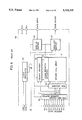
- FIG. 6 is a block diagram showing a general DRAM structure. Referring to FIG.
- a DRAM 50 comprises a memory cell array 51 for storing data signal of storage information, a row-and-column address buffer 52 for receiving external address signals to select memory cells forming a unit storage circuit, a row decoder 53 and a column decoder 54 for specifying a memory cell by decoding the address signal, a sense refresh amplifier 55 for amplifying and reading out the signal stored in the specified memory cell, a data-in buffer 56 and a data-out buffer 57 for data input/output, and a clock generator 58 for generating a clock signal.
- the memory cell array 51 occupying a large area on the semiconductor chip has a plurality of memory cells for storing unit storage information arranged in a matrix manner.
- a one-transistor one-capacitor type memory cell is well known, implemented with one MOS transistor and one capacitor connected thereof.
- Such memory cells are widely used for large capacity DRAMs because of its simple structure contributing to the improvement in higher integration of the memory cell array.
- the memory cells of a DRAM can be classified into several types depending on the structure of the capacitor.
- a stacked type capacitor can have an increased capacitor capacitance through extension of the major portion of the capacitor to the gate electrode and over the field isolation film to increase the opposing area between electrodes of the capacitor.
- a stacked type capacitor can ensure an enough capacitor capacitance even in the case devices are miniaturized by larger scale integration of the semiconductor device.
- the extensive usage of stacked type capacitors resulted from such larger scale integration of the semiconductor devices.
- development in stacked type capacitors are also in progress.
- a stacked type capacitor of a cylindrical type has been proposed to ensure constant capacitance even in the case where semiconductor devices are integrated in a more miniaturized manner.
- FIG. 7 is a sectional view of a DRAM employing a conventional stacked type capacitor of a cylindrical type.
- the DRAM adopting a conventional stacked type capacitor of a cylindrical type comprises a memory cell array and a peripheral circuit.
- the memory cell array comprises one transfer gate transistor 3 and one capacitor 10.
- the transfer gate transistor 3 comprises a pair of source/drain regions 6 formed on the surface of a P type silicon substrate 1, and gate electrodes 4b and 4c formed on the surface of P type silicon substrate 1 between one pair of source/drain regions 6 with a gate insulating film 5 thereunder.
- gate electrodes 4b and 4c are covered by an insulating film 14.
- a thick interlayer insulating film 16 is formed on the surface of silicon substrate 1 where transfer gate transistor 3 is formed.
- a capacitor 10 is implemented with a layered structure of a lower electrode (storage node) 11, a dielectric layer 12, and an upper electrode (cell plate) 13.
- One of source/drain regions 6 forming transfer gate transistor 3 is connected to a bit line 15.
- a wiring layer 18 is provided corresponding to gate electrodes 4b, 4c, and 4d.
- the peripheral circuit is implemented with two MOS transistors of identical conductivity type. That is to say, two pairs of source/drain regions 26 forming MOS transistors are provided on the P type silicon substrate.
- Gate electrodes 24c and 24d with a gate insulating film 25 thereunder are formed between one pair of source/drain regions 26.
- the MOS transistor formed on P type silicon substrate 1 is device-isolated by a field oxide film 22.
- Each of the source/drain regions 26 is connected to a wiring layer 38 via a contact layer 36.
- a stacked type capacitor has been developed for ensuring constant capacitance where devices are miniaturized in accordance with the increased scale of integration of the semiconductor device.
- Such a capacitor manufactured by a conventional method has a sectional view of FIG. 7.
- This cylindrical stacked type capacitor has the electrode formed vertically upwards from P type silicon substrate 1.
- a step is formed between the memory cell array and the peripheral circuit due to difference in height of the memory cell array and the peripheral circuit, after the formation process of the electrode.
- Such a stepped portion will lead to an inconvenience that the focus of the exposed light is offset at the stepped portion at the later photolithography processing. It was difficult to improve the patterning accuracy, with the problem that the processing accuracy could not be improved.
- There was also a difficulty in the manufacturing process due to difference in depth between the contacts of the memory cell array and the peripheral circuit, when the contact is formed after the formation of a stacked type capacitor of the cylindrical type.
- An object of the present invention is to efficiently prevent the formation of a step in the boundary region of a memory cell array and a peripheral circuit in a semiconductor memory device even of high integration.
- Another object of the present invention is to fix the potential of the boundary region of a memory cell array region and a peripheral circuit region in a semiconductor memory device.
- a further object of the present invention is to improve patterning accuracy, after the formation of a capacitor at the boundary region of a memory cell array region and a peripheral circuit region in the method of manufacturing a semiconductor memory device.
- a still further object of the present invention is to eliminate etching residue in the etching process, after the formation of a capacitor at the boundary region of a memory cell array region and a peripheral circuit region in a method of manufacturing a semiconductor memory device.
- a semiconductor memory device includes at least a memory cell array region and a peripheral circuit region formed on a semiconductor substrate, where a plurality of memory cells each having a capacitor and a transistor are formed in the memory cell array region of the semiconductor substrate.
- the transistor includes a pair of impurity regions formed on the surface of the semiconductor substrate and gate electrodes.
- the capacitor includes one electrode connected to one impurity region of the gate electrode and having a side wall extending in a vertical direction, and the other electrode arranged opposing the one electrode with a dielectric film therebetween.
- a plurality of transistors for peripheral circuits having a pair of impurity regions formed on the surface of the semiconductor substrate and a gate electrode is implemented in the peripheral circuit region of the semiconductor substrate.
- a conductor is formed at the boundary region of the memory cell array region and the peripheral circuit region of the semiconductor substrate. That conductor has a pair of standing walls extending in a vertical direction and arranged opposing each other, where at least one of the upper surface of the standing wall is located in a plane substantially identical with the upper surface of the side wall of one electrode of the capacitor.
- a conductor extends in a vertical direction between the boundary region of the memory cell array region and the peripheral circuit region in the semiconductor substrate.
- the conductor has a pair of standing walls arranged opposing each other, with at least one upper surface of the standing wall located in a plane substantially identical with the upper surface of the side wall of one electrode of the capacitor.
- the upper surface of the devices formed on the memory cell array region and the peripheral circuit region are substantially planarized.
- a method of manufacturing a semiconductor memory device comprises the steps of forming a first conductive layer convexly with an insulating film on a first device forming region, forming a second conductive layer on a second device forming region, wherein the upper surface thereof is substantially identical with the convex upper surface portion of the first conductive layer, and forming a pair of standing walls with a predetermined distance therebetween along the boundary region of the first device forming region and the second device forming region, extending vertically upwards from the main surface of the semiconductor substrate, having an upper surface substantially identical with the convex upper surface portion of the first conductive layer.
- An etch back film is formed having a thick portion and a thin portion of thickness all over the first and second device forming regions, with a stepped portion in the region between one pair of standing walls, so that the portion formed on the second device forming region is higher in height than the portion formed on the first device forming region.
- the convex upper surface portion of the first conductive layer is exposed by etch-backing the etch back film.
- the convex upper surface portion of the first conductive layer is removed, under a state where the second conductive layer still remains.
- a first conductive layer is formed convexly on the first device forming region with an insulating film therebetween.
- a second conductive layer is formed on the second device forming region, wherein the upper surface thereof is substantially identical with the convex upper surface portion of the first device forming region.
- a pair of standing walls with a predetermined distance therebetween is formed along the boundary region of the first device forming region and the second device forming region, extending vertically upwards from the main surface of the semiconductor substrate, having an upper surface substantially the same as the convex upper surface portion of the first conductive layer.
- An etch back film is formed all over the first device forming region and the second device forming region, having a thick portion and a thin portion, with a stepped portion in the region enclosed by a pair of standing walls, so that the height of the portion formed on the second device forming region is higher than the portion formed on the first device forming region.
- the convex upper surface portion of the first conductive layer is exposed by etch-backing the etch back film.
- the convex upper surface portion of the first conductive layer is removed in a state where the second conductive layer remains. As a result, the insulating film formed beneath the second conductive layer is not reduced in removing the convex upper surface portion of the first conductive layer.
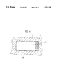
- FIG. 1 is a plan view of the structure of a DRAM of an embodiment of the present invention.
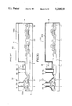
- FIG. 2 is a sectional view of the DRAM of FIG. 1.
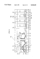
- FIGS. 3A-3H are sectional views for explaining the method of manufacturing the DRAM of FIG. 2.
- FIG. 4 is a plan view of the DRAM of FIG. 3F.
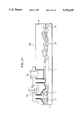
- FIG. 5 is a sectional view of a DRAM of another embodiment of the present invention.
- FIG. 6 is a block diagram of a conventional DRAM structure.
- FIG. 7 is a sectional structure view of a conventional DRAM.
- a DRAM 100 comprises a memory cell array 101 which is the storage region of data, and a peripheral circuit 102 performing operation such as applying data to or obtaining data from memory cell array 101.
- a double peripheral wall 20 is provided at the boundary region of memory cell array 101 and peripheral circuit 102.
- the number of the allocated memory cell array corresponds to the storage capacity (for example, 64M-DRAM).
- DRAM 100 comprises memory cell array 101 and peripheral circuit 102, as mentioned above.
- Memory cell array 101 comprises one transfer gate transistor 3 and one capacitor 10.
- Transfer gate transistor 3 comprises a pair of source/drain regions 6 formed on the surface of P type silicon substrate 1, and gate electrodes (word lines) 4b and 4c formed on the surface of P type silicon substrate 1 between a pair of source/drain regions 6 with a gate insulating film 5 thereunder.
- the periphery of each of gate electrodes 4b and 4c is covered by an insulating film 14.
- Capacitor 10 is implemented with a layered structure of a lower electrode (storage node) 11, a dielectric layer 12, and an upper electrode (cell plate) 13.
- Lower electrode 11 comprises a base 11a connected to source/drain regions 6 formed adjacent to field oxide film 2, and a standing wall 11b formed along the outer circumference of base 11a extending vertically upwards.
- Base 11a and standing wall 11b are formed integrally of a polycrystal silicon layer having impurities introduced.
- Dielectric layer 12 is formed on the surface of lower electrode 11.
- Dielectric layer 12 is formed to cover both sides of the inner side and the outer side of standing wall 11b of lower electrode 11.
- the standing wall 11b of lower electrode 11 forms the capacitance portion with both the inner and outer sides to effectively ensure constant capacitance when miniaturized.
- Dielectric layer 12 may comprise, for example, an oxide film, a nitride film, a composite film of an oxide film and a nitride film, a metal oxide film or the like.
- the surface of upper electrode 13 is covered by an interlayer insulating film 16.
- a wiring layer 18 of a predetermined configuration is formed on the surface of interlayer insulating film 16.
- Bit line 15 is formed at a position lower than standing wall 11b and the main portion of base 11a of lower electrode 11.
- One of source/drain regions 6 of transfer gate transistor 3 extends to a region contacting bit line 15.
- Contact with bit line 15 is implemented with the connection of the extending source/drain regions 6 and bit line 15.
- Peripheral circuit 102 has two MOS transistors formed of the same conductivity type. That is to say, source/drain regions 26 are formed on P type silicon substrate 1, corresponding to the number of the MOS transistors. The MOS transistors are isolated by field oxide film 22. Source/drain regions 26 are formed to connect conductive layers 31a and 35. A wiring layer 38 is formed above conductive layers 31a and 35 with a contact layer 36 therebetween. Gate electrodes 24c and 24d are formed between one pair of source/drain regions 26 with a gate insulating film 25 thereunder. An insulating film 14 is formed over each of gate electrodes 24c and 24d.
- the boundary region of memory cell array 101 and peripheral circuit 102 is formed with a double peripheral wall 20. That is to say, peripheral walls 20a and 20b are formed above field oxide film 2 of P type silicon substrate 1, extending vertically upwards from P type silicon substrate 1, with base 11a constituting lower electrode 11 of capacitor 10 of memory cell array 101 thereunder.
- This double peripheral wall 20 is formed to enclose the region where memory cell array 101 is formed, as shown in FIG. 1.
- the potential of the periphery of memory cell array 101 can be fixed by adjusting the potential of base 11a of double periphery wall 20 to a predetermined potential.
- Field oxide films 2 and 22 are formed on P type silicon substrate 1. Then, source/drain regions 6 and gate electrodes 4b and 4c are formed implementing transfer gate transistor 3 of the memory cell array. Source/drain regions 26 and gate electrodes 24c and 24d are formed implementing two MOS transistors of the peripheral circuit. Bit line 15 is formed at source/drain regions 6 of the memory cell array. Simultaneously, conductive layers 31a and 31b are formed on source/drain regions 26 of the peripheral circuit. Insulating film 21, and insulating films 33a and 33b are formed on bit line 15, and conductive layers 31a and 31b, respectively.
- a polycrystal silicon layer 110a having impurities introduced is deposited, and conductive layer 35 is formed in the peripheral circuit by patterning. Then, an oxide film 45 is formed on the whole surface, as shown in FIG. 3B. A resist 46 is formed over oxide film 45, as shown in FIG. 3C. Only the memory cell array region of the region where resist 46 is formed is patterned to carry out dry etching anisotropically. After resist 46 is removed, a polycrystal silicon layer 110b is formed on the whole surface, as shown in FIG. 3D. Then, an etch back film 47 is formed all over polycrystal silicon layer 110b, as shown in FIG. 3E.
- Etch back film 47 is etched-back to expose the top surface of polycrystal silicon layer 110b formed on the memory cell array. Oxide films and resists are used for etch back film 47. As shown in FIG. 3F, a resist 48 is formed all over the surface, with a stepped portion formed in the region between peripheral walls 20a and 20b of the double peripheral wall 20. The top surface of the exposed polycrystal silicon layer 110b of the memory cell array is selectively removed by etching. This step of FIG. 3F indicates that the region outside the center line of the double peripheral wall 20 formed at the boundary region of memory cell array 101 and peripheral circuit 102 is covered by resist 48, as shown in the plan view of FIG. 4. The sectional view taken along line X--X of FIG. 4 corresponds to FIG.
- oxide films 45 and 47 are removed, as shown in FIG. 3G.
- Polysilicon layer 110a (refer to FIG. 3F) is patterned in self-alignment to form base 11a. Resist 48 is then removed.
- a polycrystal silicon layer 13 is deposited, after dielectric layer 12 is formed on the whole surface. Then, other portions are removed to leave upper electrode 13 and dielectric film 12 only on the memory cell array by patterning.
- peripheral walls 20a and 20b are formed implementing the double layer peripheral wall 20.
- capacitor 10 is formed implemented with base 11a and standing wall 11b of a polycrystal silicon layer, dielectric film 12, and an upper layer electrode 13 of polycrystal silicon layer.
- Interlayer insulating film 16 is deposited on the whole surface to form contact layer 36 of the peripheral circuit. Then, wiring layers 18 and 38 are formed in the corresponding portion.
- the DRAM 100 of FIG. 2 is formed.
- this DRAM differs from that of FIG. 2 in that an impurity diffusion layer 40 is formed between field oxide films 2a and 2b formed on P type silicon substrate 1. There is also difference in that base 11a is formed to connect impurity diffusion layer 40, and that peripheral walls 20a and 20b constituting the double periphery wall 20 are formed above base 11a.
- Such a structure allows the achievement of fixing the potential of double peripheral wall 20 by adjusting the potential of impurity diffusion layer 40. As a result, the potential of the boundary region of memory cell array 101 and peripheral wall 102 can be fixed.
- the semiconductor memory device in accordance with the present embodiment comprises a conductor having a pair of standing walls arranged opposing each other, extending in a vertical direction at the boundary region between the memory cell array and the peripheral wall.
- the method of manufacturing a semiconductor memory device of the present invention comprises the step of forming a first conductive film convexly on a first device forming region with an insulating film therebetween.
- a second conductive layer is formed on the second device forming region, wherein the upper surface is substantially the same as the convex upper surface portion of the first conductive layer.
- a pair of standing walls are formed with a predetermined distance therebetween along the boundary region of the first device forming region and the second device forming region, extending vertically upwards from the main surface of the semiconductor substrate, wherein the upper surface is substantially equal to the convex upper layer of the first conductive layer.
- An etch back film having a thick portion and a thin portion is formed all over the first device forming region and the second device forming region, with a stepped portion in the region between the pair of standing walls, so that the portion formed on the second device forming region is higher than the region formed on the first device forming region.
- the etch back film is etched back to expose the convex upper surface portion of the first conductive layer.
Landscapes
- Engineering & Computer Science (AREA)
- Manufacturing & Machinery (AREA)
- Semiconductor Memories (AREA)
- Semiconductor Integrated Circuits (AREA)
Priority Applications (1)
| Application Number | Priority Date | Filing Date | Title |
|---|---|---|---|
| US08/017,901 US5364811A (en) | 1990-04-27 | 1993-02-16 | Method of manufacturing a semiconductor memory device with multiple device forming regions |
Applications Claiming Priority (2)
| Application Number | Priority Date | Filing Date | Title |
|---|---|---|---|
| JP2-113633 | 1990-04-27 | ||
| JP2113633A JP2519569B2 (ja) | 1990-04-27 | 1990-04-27 | 半導体記憶装置およびその製造方法 |
Related Child Applications (1)
| Application Number | Title | Priority Date | Filing Date |
|---|---|---|---|
| US08/017,901 Division US5364811A (en) | 1990-04-27 | 1993-02-16 | Method of manufacturing a semiconductor memory device with multiple device forming regions |
Publications (1)
| Publication Number | Publication Date |
|---|---|
| US5218219A true US5218219A (en) | 1993-06-08 |
Family
ID=14617183
Family Applications (2)
| Application Number | Title | Priority Date | Filing Date |
|---|---|---|---|
| US07/678,872 Expired - Lifetime US5218219A (en) | 1990-04-27 | 1991-04-04 | Semiconductor memory device having a peripheral wall at the boundary region of a memory cell array region and a peripheral circuit region |
| US08/017,901 Expired - Lifetime US5364811A (en) | 1990-04-27 | 1993-02-16 | Method of manufacturing a semiconductor memory device with multiple device forming regions |
Family Applications After (1)
| Application Number | Title | Priority Date | Filing Date |
|---|---|---|---|
| US08/017,901 Expired - Lifetime US5364811A (en) | 1990-04-27 | 1993-02-16 | Method of manufacturing a semiconductor memory device with multiple device forming regions |
Country Status (4)
| Country | Link |
|---|---|
| US (2) | US5218219A (ja) |
| JP (1) | JP2519569B2 (ja) |
| KR (1) | KR940005888B1 (ja) |
| DE (1) | DE4113233C2 (ja) |
Cited By (21)
| Publication number | Priority date | Publication date | Assignee | Title |
|---|---|---|---|---|
| US5306945A (en) * | 1992-10-27 | 1994-04-26 | Micron Semiconductor, Inc. | Feature for a semiconductor device to reduce mobile ion contamination |
| US5332687A (en) * | 1992-06-12 | 1994-07-26 | Sony Corporation | Method of manufacturing a semiconductor memory having a memory cell array and a peripheral circuit portion so as to improve the characteristics of the device |
| US5346843A (en) * | 1991-04-30 | 1994-09-13 | Sony Corporation | Method of manufacturing a semiconductor device having a memory cell and peripheral circuit including forming a first electrode for the capacitor |
| US5381365A (en) * | 1990-01-26 | 1995-01-10 | Mitsubishi Denki Kabushiki Kaisha | Dynamic random access memory having stacked type capacitor and manufacturing method therefor |
| US5391511A (en) * | 1992-02-19 | 1995-02-21 | Micron Technology, Inc. | Semiconductor processing method of producing an isolated polysilicon lined cavity and a method of forming a capacitor |
| US5420462A (en) * | 1993-04-13 | 1995-05-30 | Kabushiki Kaisha Toshiba | Semiconductor device with conductors on stepped substrate having planar upper surfaces |
| US5438011A (en) * | 1995-03-03 | 1995-08-01 | Micron Technology, Inc. | Method of forming a capacitor using a photoresist contact sidewall having standing wave ripples |
| US5449636A (en) * | 1993-07-27 | 1995-09-12 | Hyundai Electronics Industries Co., Ltd. | Method for the fabrication of DRAM cell having a trench in the field oxide |
| US5481127A (en) * | 1992-11-04 | 1996-01-02 | Mitsubishi Denki Kabushiki Kaisha | Semiconductor memory device having a capacitor |
| US5497025A (en) * | 1994-04-22 | 1996-03-05 | Chartered Semiconductor Manufacturing | Methods to fabricate large highly reflective metal reflector plates for applications in game chips or similar virtual image projection use |
| US5539612A (en) * | 1992-09-08 | 1996-07-23 | Texas Instruments Incorporated | Intermediate structure for forming a storage capacitor |
| US5539230A (en) * | 1995-03-16 | 1996-07-23 | International Business Machines Corporation | Chimney capacitor |
| US5597755A (en) * | 1990-01-26 | 1997-01-28 | Mitsubishi Denki Kabushiki Kaisha | Method of manufacturing a stacked capacitor in a dram |
| US5714779A (en) * | 1992-06-30 | 1998-02-03 | Siemens Aktiengesellschaft | Semiconductor memory device having a transistor, a bit line, a word line and a stacked capacitor |
| US5731610A (en) * | 1995-03-07 | 1998-03-24 | Micron Technology, Inc. | Semiconductor device having improved contacts to a thin conductive layer |
| US5965939A (en) * | 1992-04-16 | 1999-10-12 | Samsung Electronics Co., Ltd. | Semiconductor device and a method of manufacture |
| US6043118A (en) * | 1990-11-30 | 2000-03-28 | Hitachi, Ltd. | Semiconductor memory circuit device and method for fabricating a semiconductor memory device circuit |
| US6255151B1 (en) | 1997-12-19 | 2001-07-03 | Hitachi, Ltd. | Semiconductor integrated circuit device and method of manufacturing same |
| US20020109162A1 (en) * | 1999-09-02 | 2002-08-15 | Er-Xuan Ping | Reduction of shorts among electrical cells formed on a semiconductor substrate |
| KR100375428B1 (ko) * | 1995-11-20 | 2003-05-17 | 가부시끼가이샤 히다치 세이사꾸쇼 | 반도체기억장치 및 그 제조방법 |
| US6861694B2 (en) * | 1996-11-06 | 2005-03-01 | Fujitsu Limited | Semiconductor device and method for fabricating the same |
Families Citing this family (28)
| Publication number | Priority date | Publication date | Assignee | Title |
|---|---|---|---|---|
| IT1245495B (it) * | 1990-01-26 | 1994-09-27 | Mitsubishi Electric Corp | Memoria ad accesso casuale dinamica avente un condensatore del tipo impilato e procedimento di fabbricazione di essa |
| DE4143476C2 (de) * | 1990-01-26 | 2001-03-08 | Mitsubishi Electric Corp | Verfahren zum Herstellen einer Halbleiterspeichervorrichtung |
| US5276344A (en) * | 1990-04-27 | 1994-01-04 | Mitsubishi Denki Kabushiki Kaisha | Field effect transistor having impurity regions of different depths and manufacturing method thereof |
| JP2524862B2 (ja) * | 1990-05-01 | 1996-08-14 | 三菱電機株式会社 | 半導体記憶装置およびその製造方法 |
| JP2535676B2 (ja) * | 1991-04-01 | 1996-09-18 | 株式会社東芝 | 半導体装置の製造方法 |
| KR960003864B1 (ko) * | 1992-01-06 | 1996-03-23 | 삼성전자주식회사 | 반도체 메모리장치 및 그 제조방법 |
| JP2769664B2 (ja) * | 1992-05-25 | 1998-06-25 | 三菱電機株式会社 | 半導体記憶装置およびその製造方法 |
| DE4221434A1 (de) * | 1992-06-30 | 1994-01-05 | Siemens Ag | Herstellverfahren für einen Speicherkondensator |
| DE4222467C1 (ja) * | 1992-07-08 | 1993-06-24 | Siemens Ag, 8000 Muenchen, De | |
| JP2620529B2 (ja) * | 1993-12-28 | 1997-06-18 | 現代電子産業株式会社 | ディーラム キャパシター製造方法 |
| US5501998A (en) * | 1994-04-26 | 1996-03-26 | Industrial Technology Research Institution | Method for fabricating dynamic random access memory cells having vertical sidewall stacked storage capacitors |
| KR100304946B1 (ko) * | 1994-07-08 | 2001-11-30 | 김영환 | 반도체장치의제조방법 |
| JP3520114B2 (ja) * | 1994-07-11 | 2004-04-19 | 株式会社ルネサステクノロジ | 半導体装置の製造方法 |
| JPH08153858A (ja) * | 1994-11-29 | 1996-06-11 | Nec Corp | 半導体装置の製造方法 |
| US5550077A (en) * | 1995-05-05 | 1996-08-27 | Vanguard International Semiconductor Corporation | DRAM cell with a comb-type capacitor |
| JPH0936308A (ja) * | 1995-07-14 | 1997-02-07 | Matsushita Electron Corp | 半導体装置の製造方法 |
| JPH0992717A (ja) * | 1995-09-21 | 1997-04-04 | Mitsubishi Electric Corp | 半導体装置およびその製造方法 |
| US5670410A (en) * | 1996-09-25 | 1997-09-23 | Chartered Semiconductor Manufacturing Pte Ltd. | Method of forming integrated CMP stopper and analog capacitor |
| TW377495B (en) | 1996-10-04 | 1999-12-21 | Hitachi Ltd | Method of manufacturing semiconductor memory cells and the same apparatus |
| JP3869089B2 (ja) | 1996-11-14 | 2007-01-17 | 株式会社日立製作所 | 半導体集積回路装置の製造方法 |
| US5723374A (en) * | 1996-12-27 | 1998-03-03 | Taiwan Semiconductor Manufacturing Company, Ltd. | Method for forming dielectric spacer to prevent poly stringer in stacked capacitor DRAM technology |
| US6258662B1 (en) * | 1997-05-06 | 2001-07-10 | Taiwan Semiconductor Manufacturing Co., Ltd. | Method for forming cylindrical DRAM capacitors |
| KR100269317B1 (ko) * | 1997-12-09 | 2000-12-01 | 윤종용 | 평탄화를위한반도체장치및그제조방법 |
| US6596577B2 (en) * | 1998-08-25 | 2003-07-22 | Micron Technology, Inc. | Semiconductor processing methods of forming dynamic random access memory (DRAM) circuitry |
| JP2000188383A (ja) * | 1998-10-14 | 2000-07-04 | Fujitsu Ltd | 半導体装置およびその製造方法、半導体集積回路およびその製造方法 |
| JP3445965B2 (ja) | 2000-08-24 | 2003-09-16 | 松下電器産業株式会社 | 半導体装置およびその製造方法 |
| WO2006080550A1 (en) * | 2005-01-31 | 2006-08-03 | Semiconductor Energy Laboratory Co., Ltd. | Memory device and semiconductor device |
| US8604547B2 (en) * | 2005-02-10 | 2013-12-10 | Semiconductor Energy Laboratory Co., Ltd. | Memory element and semiconductor device |
Citations (5)
| Publication number | Priority date | Publication date | Assignee | Title |
|---|---|---|---|---|
| DE3918924A1 (de) * | 1988-06-10 | 1989-12-14 | Mitsubishi Electric Corp | Halbleiterspeichereinrichtung vom gestapelten kondensatortyp und herstellungsverfahren dafuer |
| US4958318A (en) * | 1988-07-08 | 1990-09-18 | Eliyahou Harari | Sidewall capacitor DRAM cell |
| US4994893A (en) * | 1988-09-29 | 1991-02-19 | Mitsubishi Denki Kabushiki Kaisha | Field effect transistor substantially coplanar surface structure |
| EP0414227A1 (en) * | 1989-08-24 | 1991-02-27 | Nec Corporation | Dynamic random access memory device having rampart structure outside memory cell array |
| US5047817A (en) * | 1988-06-10 | 1991-09-10 | Mitsubishi Denki Kabushiki Kasiha | Stacked capacitor for semiconductor memory device |
Family Cites Families (4)
| Publication number | Priority date | Publication date | Assignee | Title |
|---|---|---|---|---|
| JP2723530B2 (ja) * | 1988-04-13 | 1998-03-09 | 日本電気株式会社 | ダイナミック型ランダムアクセスメモリ装置の製造方法 |
| JP2768758B2 (ja) * | 1989-10-04 | 1998-06-25 | 株式会社東芝 | 半導体記憶装置及びその製造方法 |
| US5049517A (en) * | 1990-11-07 | 1991-09-17 | Micron Technology, Inc. | Method for formation of a stacked capacitor |
| US5053351A (en) * | 1991-03-19 | 1991-10-01 | Micron Technology, Inc. | Method of making stacked E-cell capacitor DRAM cell |
-
1990
- 1990-04-27 JP JP2113633A patent/JP2519569B2/ja not_active Expired - Fee Related
-
1991
- 1991-03-02 KR KR1019910003428A patent/KR940005888B1/ko not_active Expired - Fee Related
- 1991-04-04 US US07/678,872 patent/US5218219A/en not_active Expired - Lifetime
- 1991-04-23 DE DE4113233A patent/DE4113233C2/de not_active Expired - Fee Related
-
1993
- 1993-02-16 US US08/017,901 patent/US5364811A/en not_active Expired - Lifetime
Patent Citations (5)
| Publication number | Priority date | Publication date | Assignee | Title |
|---|---|---|---|---|
| DE3918924A1 (de) * | 1988-06-10 | 1989-12-14 | Mitsubishi Electric Corp | Halbleiterspeichereinrichtung vom gestapelten kondensatortyp und herstellungsverfahren dafuer |
| US5047817A (en) * | 1988-06-10 | 1991-09-10 | Mitsubishi Denki Kabushiki Kasiha | Stacked capacitor for semiconductor memory device |
| US4958318A (en) * | 1988-07-08 | 1990-09-18 | Eliyahou Harari | Sidewall capacitor DRAM cell |
| US4994893A (en) * | 1988-09-29 | 1991-02-19 | Mitsubishi Denki Kabushiki Kaisha | Field effect transistor substantially coplanar surface structure |
| EP0414227A1 (en) * | 1989-08-24 | 1991-02-27 | Nec Corporation | Dynamic random access memory device having rampart structure outside memory cell array |
Cited By (35)
| Publication number | Priority date | Publication date | Assignee | Title |
|---|---|---|---|---|
| US5798289A (en) * | 1990-01-26 | 1998-08-25 | Mitsubishi Denki Kabushiki Kaisha | Method of manufacturing stacked capacitors in a DRAM with reduced isolation region between adjacent capacitors |
| US5597755A (en) * | 1990-01-26 | 1997-01-28 | Mitsubishi Denki Kabushiki Kaisha | Method of manufacturing a stacked capacitor in a dram |
| US5381365A (en) * | 1990-01-26 | 1995-01-10 | Mitsubishi Denki Kabushiki Kaisha | Dynamic random access memory having stacked type capacitor and manufacturing method therefor |
| US6043118A (en) * | 1990-11-30 | 2000-03-28 | Hitachi, Ltd. | Semiconductor memory circuit device and method for fabricating a semiconductor memory device circuit |
| US5346843A (en) * | 1991-04-30 | 1994-09-13 | Sony Corporation | Method of manufacturing a semiconductor device having a memory cell and peripheral circuit including forming a first electrode for the capacitor |
| US5391511A (en) * | 1992-02-19 | 1995-02-21 | Micron Technology, Inc. | Semiconductor processing method of producing an isolated polysilicon lined cavity and a method of forming a capacitor |
| US5965939A (en) * | 1992-04-16 | 1999-10-12 | Samsung Electronics Co., Ltd. | Semiconductor device and a method of manufacture |
| US5332687A (en) * | 1992-06-12 | 1994-07-26 | Sony Corporation | Method of manufacturing a semiconductor memory having a memory cell array and a peripheral circuit portion so as to improve the characteristics of the device |
| US5714779A (en) * | 1992-06-30 | 1998-02-03 | Siemens Aktiengesellschaft | Semiconductor memory device having a transistor, a bit line, a word line and a stacked capacitor |
| US5604659A (en) * | 1992-09-08 | 1997-02-18 | Texas Instruments Incorporated | Microelectronic device with centered storage capacitor cavity sized less than feature size |
| US5539612A (en) * | 1992-09-08 | 1996-07-23 | Texas Instruments Incorporated | Intermediate structure for forming a storage capacitor |
| US5712182A (en) * | 1992-09-08 | 1998-01-27 | Texas Instruments Incorporated | Method of forming a microelectronic device having a cavity smaller than lithographic tolerances |
| US5306945A (en) * | 1992-10-27 | 1994-04-26 | Micron Semiconductor, Inc. | Feature for a semiconductor device to reduce mobile ion contamination |
| US5481127A (en) * | 1992-11-04 | 1996-01-02 | Mitsubishi Denki Kabushiki Kaisha | Semiconductor memory device having a capacitor |
| US5602050A (en) * | 1993-04-13 | 1997-02-11 | Kabushiki Kaisha Toshiba | Method of making a semiconductor device with conductors on stepped substrate having planar upper surfaces |
| US5420462A (en) * | 1993-04-13 | 1995-05-30 | Kabushiki Kaisha Toshiba | Semiconductor device with conductors on stepped substrate having planar upper surfaces |
| DE4426468C2 (de) * | 1993-07-27 | 2002-10-10 | Hyundai Electronics Ind | Verfahren zur Herstellung einer DRAM-Zelle |
| US5449636A (en) * | 1993-07-27 | 1995-09-12 | Hyundai Electronics Industries Co., Ltd. | Method for the fabrication of DRAM cell having a trench in the field oxide |
| US5497025A (en) * | 1994-04-22 | 1996-03-05 | Chartered Semiconductor Manufacturing | Methods to fabricate large highly reflective metal reflector plates for applications in game chips or similar virtual image projection use |
| US5438011A (en) * | 1995-03-03 | 1995-08-01 | Micron Technology, Inc. | Method of forming a capacitor using a photoresist contact sidewall having standing wave ripples |
| US20050282377A1 (en) * | 1995-03-07 | 2005-12-22 | Rhodes Howard E | Method of making a semiconductor device having improved contacts |
| US7932174B2 (en) | 1995-03-07 | 2011-04-26 | Micron Technology, Inc. | Method of making a semiconductor device having improved contacts |
| US20090087987A1 (en) * | 1995-03-07 | 2009-04-02 | Micron Technology Inc. | Method of making a semiconductor device having improved contacts |
| US5731610A (en) * | 1995-03-07 | 1998-03-24 | Micron Technology, Inc. | Semiconductor device having improved contacts to a thin conductive layer |
| US5539230A (en) * | 1995-03-16 | 1996-07-23 | International Business Machines Corporation | Chimney capacitor |
| US7196368B2 (en) | 1995-11-20 | 2007-03-27 | Renesas Technology Corp. | Semiconductor memory arrangements with crown shaped capacitor arrangements trenched in interlayer dielectric film |
| KR100375428B1 (ko) * | 1995-11-20 | 2003-05-17 | 가부시끼가이샤 히다치 세이사꾸쇼 | 반도체기억장치 및 그 제조방법 |
| US6617205B1 (en) | 1995-11-20 | 2003-09-09 | Hitachi, Ltd. | Semiconductor storage device and process for manufacturing the same |
| US6791134B2 (en) | 1995-11-20 | 2004-09-14 | Hitachi, Ltd. | Semiconductor memory device and manufacturing method thereof |
| US6798005B2 (en) | 1995-11-20 | 2004-09-28 | Hitachi, Ltd. | Semiconductor memory device having large storage capacity and minimal step height between memory cell and peripheral circuits |
| US20050045933A1 (en) * | 1995-11-20 | 2005-03-03 | Shinichiro Kimura | Semiconductor memory device and manufacturing method thereof |
| US6861694B2 (en) * | 1996-11-06 | 2005-03-01 | Fujitsu Limited | Semiconductor device and method for fabricating the same |
| US6423992B2 (en) | 1997-12-19 | 2002-07-23 | Hitachi, Ltd. | Semiconductor integrated circuit device |
| US6255151B1 (en) | 1997-12-19 | 2001-07-03 | Hitachi, Ltd. | Semiconductor integrated circuit device and method of manufacturing same |
| US20020109162A1 (en) * | 1999-09-02 | 2002-08-15 | Er-Xuan Ping | Reduction of shorts among electrical cells formed on a semiconductor substrate |
Also Published As
| Publication number | Publication date |
|---|---|
| KR910019230A (ko) | 1991-11-30 |
| JPH0410651A (ja) | 1992-01-14 |
| JP2519569B2 (ja) | 1996-07-31 |
| DE4113233A1 (de) | 1991-10-31 |
| US5364811A (en) | 1994-11-15 |
| KR940005888B1 (ko) | 1994-06-24 |
| DE4113233C2 (de) | 1994-06-30 |
Similar Documents
| Publication | Publication Date | Title |
|---|---|---|
| US5218219A (en) | Semiconductor memory device having a peripheral wall at the boundary region of a memory cell array region and a peripheral circuit region | |
| US5216266A (en) | Semiconductor memory device having memory cells formed in trench and manufacturing method therefor | |
| US5047817A (en) | Stacked capacitor for semiconductor memory device | |
| US5659191A (en) | DRAM having peripheral circuitry in which source-drain interconnection contact of a MOS transistor is made small by utilizing a pad layer and manufacturing method thereof | |
| US5032882A (en) | Semiconductor device having trench type structure | |
| EP0337436A2 (en) | Semiconductor memory device having improved dynamic memory cell structure | |
| US5338955A (en) | Semiconductor device having stacked type capacitor | |
| US6004844A (en) | Unit cell layout and transfer gate design for high density DRAMs | |
| US5285092A (en) | Semiconductor memory device having a stacked type capacitor and manufacturing method therefor | |
| US5393688A (en) | Method of manufacturing a stacked capacitor DRAM | |
| US5448512A (en) | Semiconductor memory device with contact region intermediate memory cell and peripheral circuit | |
| US5247196A (en) | Semiconductor memory device including capacitor having stacked structure and manufacturing method thereof | |
| US5606189A (en) | Dynamic RAM trench capacitor device with contact strap | |
| US5229314A (en) | Method of manufacturing field effect transistor having a multilayer interconnection layer therein with tapered sidewall insulation | |
| US6188099B1 (en) | Storage capacitor structure | |
| US5183774A (en) | Method of making a semiconductor memory device | |
| US5180683A (en) | Method of manufacturing stacked capacitor type semiconductor memory device | |
| US5027173A (en) | Semiconductor memory device with two separate gates per block | |
| US5281838A (en) | Semiconductor device having contact between wiring layer and impurity region | |
| JP2715012B2 (ja) | 半導体記憶装置およびその製造方法 | |
| US5219781A (en) | Method for manufacturing semiconductor memory device having a stacked type capacitor | |
| US4173819A (en) | Method of manufacturing a dynamic random access memory using MOS FETS | |
| JPH04343266A (ja) | 半導体記憶装置及びその製造方法 | |
| US5157469A (en) | Field effect transistor having a multilayer interconnection layer therein with tapered sidewall insulators | |
| US6110776A (en) | Method for forming bottom electrode of capacitor |
Legal Events
| Date | Code | Title | Description |
|---|---|---|---|
| AS | Assignment |
Owner name: MITSUBISHI DENKI KABUSHIKI KAISHA, JAPAN Free format text: ASSIGNMENT OF ASSIGNORS INTEREST.;ASSIGNORS:AJIKA, NATSUO;ARIMA, HIDEAKI;MOTONAMI, KAORU;AND OTHERS;REEL/FRAME:005777/0241 Effective date: 19910517 |
|
| STCF | Information on status: patent grant |
Free format text: PATENTED CASE |
|
| FEPP | Fee payment procedure |
Free format text: PAYOR NUMBER ASSIGNED (ORIGINAL EVENT CODE: ASPN); ENTITY STATUS OF PATENT OWNER: LARGE ENTITY |
|
| FPAY | Fee payment |
Year of fee payment: 4 |
|
| FPAY | Fee payment |
Year of fee payment: 8 |
|
| FPAY | Fee payment |
Year of fee payment: 12 |