US20160018754A1 - Light emission element array chip, chip mounting substrate, and image forming apparatus - Google Patents
Light emission element array chip, chip mounting substrate, and image forming apparatus Download PDFInfo
- Publication number
- US20160018754A1 US20160018754A1 US14/715,901 US201514715901A US2016018754A1 US 20160018754 A1 US20160018754 A1 US 20160018754A1 US 201514715901 A US201514715901 A US 201514715901A US 2016018754 A1 US2016018754 A1 US 2016018754A1
- Authority
- US
- United States
- Prior art keywords
- light emission
- emission element
- element array
- chip
- scanning direction
- Prior art date
- Legal status (The legal status is an assumption and is not a legal conclusion. Google has not performed a legal analysis and makes no representation as to the accuracy of the status listed.)
- Abandoned
Links
- 239000000758 substrate Substances 0.000 title claims description 36
- 230000008901 benefit Effects 0.000 description 2
- 230000003287 optical effect Effects 0.000 description 2
- 238000005452 bending Methods 0.000 description 1
- 230000015556 catabolic process Effects 0.000 description 1
- 238000006731 degradation reaction Methods 0.000 description 1
- 230000006866 deterioration Effects 0.000 description 1
- 230000000694 effects Effects 0.000 description 1
- 238000005401 electroluminescence Methods 0.000 description 1
- 238000005516 engineering process Methods 0.000 description 1
- 238000004519 manufacturing process Methods 0.000 description 1
- 238000012986 modification Methods 0.000 description 1
- 230000004048 modification Effects 0.000 description 1
- 239000013589 supplement Substances 0.000 description 1
Images


Classifications
-
- G—PHYSICS
- G03—PHOTOGRAPHY; CINEMATOGRAPHY; ANALOGOUS TECHNIQUES USING WAVES OTHER THAN OPTICAL WAVES; ELECTROGRAPHY; HOLOGRAPHY
- G03G—ELECTROGRAPHY; ELECTROPHOTOGRAPHY; MAGNETOGRAPHY
- G03G15/00—Apparatus for electrographic processes using a charge pattern
- G03G15/04—Apparatus for electrographic processes using a charge pattern for exposing, i.e. imagewise exposure by optically projecting the original image on a photoconductive recording material
- G03G15/04036—Details of illuminating systems, e.g. lamps, reflectors
- G03G15/04045—Details of illuminating systems, e.g. lamps, reflectors for exposing image information provided otherwise than by directly projecting the original image onto the photoconductive recording material, e.g. digital copiers
- G03G15/04054—Details of illuminating systems, e.g. lamps, reflectors for exposing image information provided otherwise than by directly projecting the original image onto the photoconductive recording material, e.g. digital copiers by LED arrays
-
- F—MECHANICAL ENGINEERING; LIGHTING; HEATING; WEAPONS; BLASTING
- F21—LIGHTING
- F21V—FUNCTIONAL FEATURES OR DETAILS OF LIGHTING DEVICES OR SYSTEMS THEREOF; STRUCTURAL COMBINATIONS OF LIGHTING DEVICES WITH OTHER ARTICLES, NOT OTHERWISE PROVIDED FOR
- F21V19/00—Fastening of light sources or lamp holders
Definitions
- the present invention relates to a light emission element array chip, a chip mounting substrate, and an image forming apparatus.
- line heads such as light emission array heads or so.
- the line head irradiates an electrified surface of a photoconductor drum to form an electrostatic latent image; a toner image is formed as a result of a toner being put on the electrostatic latent image (developing); and the toner image is transferred to paper and is fixed there.
- the distance between light emission elements is as small as approximately 21 ⁇ m.
- the chip mounting error may be on the order of ⁇ 6 ⁇ m and the distance between a light emission element and a chip edge may be on the order of 3 ⁇ m. Therefore, it may be necessary to set the side length of a light emission element to be 3 ⁇ m. Note that, actually, by further considering a chip dicing error, it may be necessary to further reduce the size of a light emission element.
- Exposure energy given to a photoconductor by a light emission element is in proportion to the size of the light emission element.
- the size of a light emission element being reduced as mentioned above, exposure energy given to a photoconductor may become insufficient.
- the service life of the light emission element may be reduced accordingly, and therefore, but the service life of the apparatus employing the light emission elements may become insufficient.
- Japanese Laid-Open Patent Application No. 09-263004 discloses a configuration where LED chips are arranged in such a manner that the adjacent LED chips overlap each other along the light emission element arranging direction.
- Japanese Laid-Open Patent Application No. 10-244706 discloses a configuration where the width of light emission elements at the end parts of light emission element array chips is reduced in comparison to the other light emission elements.
- a light emission element array chip has a plurality of light emission element groups arranged thereon.
- Each of the light emission element groups includes N light emission elements arranged in a sub-scanning direction, where N denotes a natural number.
- the light emission element groups include a first block of the light emission element groups arranged at intervals of a first predetermined distance in a main-scanning direction; and a second block of one or more of the light emission element groups at either end side of the light emission element array chip shifted from a reference position by a second predetermined distance in the sub-scanning direction, the reference position being a position of each light emission element group included in the first block of the light emission element groups.
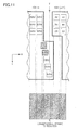
- FIG. 1 is a general side view illustrating a configuration of an image forming apparatus 100 according to a first embodiment of the present invention
- FIG. 2 is a plan view of a chip mounting substrate 1 shown in FIG. 1 ;
- FIG. 3A is a magnified view of an area E of FIG. 2 ;
- FIG. 3B is a view corresponding to FIG. 3A illustrating a case where a chip edge is shaped in a manner of being bent at a predetermined angle;
- FIG. 3C is a view corresponding to FIG. 3A illustrating a case where the number of light emission element groups included in a second block of one or more of light emission element groups is increased;
- FIG. 4 is a general side view illustrating a configuration of an image forming apparatus 100 A according to a second embodiment of the present invention
- FIG. 5 is a magnified view of an end part of a light emission element array chip shown in FIG. 4 ;
- FIG. 6 includes, in an upper part, a magnified view of an end part of a light emission array chip 10 - m illustrating a first state of adjacently arranging the light emission element array chip 10 - m and a light emission element array chip 10 -( m+ 1) of FIG. 2 , and, in a lower part, a general view illustrating a printing result of the state of the upper part;
- FIG. 7 includes, in an upper part, a magnified view of the end part of the light emission array chip 10 A-m illustrating the first state of adjacently arranging the light emission element array chip 10 A-m and the light emission element array chip 10 A-(m+1) of FIG. 5 , and, in a lower part, a general view illustrating a printing result of the state of the upper part;
- FIG. 8 includes, in an upper part, a magnified view of the end part of the light emission array chip 10 - m illustrating a second state of adjacently arranging the light emission element array chip 10 - m and the light emission element array chip 10 -( m+ 1) of FIG. 2 , and, in a lower part, a general view illustrating a printing result of the state of the upper part;
- FIG. 9 includes, in an upper part, a magnified view of the end part of the light emission array chip 10 A-m illustrating the second state of adjacently arranging the light emission element array chip 10 A-m and the light emission element array chip 10 A-(m+1) of FIG. 5 , and, in a lower part, a general view illustrating a printing result of the state of the upper part;
- FIG. 10 includes, in an upper part, a magnified view of the end part of the light emission array chip 10 - m illustrating a third state of adjacently arranging the light emission element array chip 10 - m and the light emission element array chip 10 -( m+ 1) of FIG. 2 , and, in a lower part, a general view illustrating a printing result of the state of the upper part; and
- FIG. 11 includes, in an upper part, a magnified view of the end part of the light emission array chip 10 A-m illustrating the third state of adjacently arranging the light emission element array chip 10 A-m and the light emission element array chip 10 A-(m+1) of FIG. 5 , and, in a lower part, a general view illustrating a printing result of the state of the upper part.
- the embodiments of the present invention relate to light emission element array chips and chip mounting substrates for image forming apparatuses such as copiers, printers, facsimile machines, or so, and the image forming apparatuses.
- the head width may thus increase, the size of the apparatus including them may increase, and thus, the cost may increase. Also, printing is carried out from light emission points shifted in the sub-scanning direction, and therefore, light emission control may become complicated; thus the cost required for the control may increase.
- the light emission elements at the end parts of the light emission element array chip are smaller than the other light emission elements. Therefore, it may be necessary to increase the current amount supplied to the light emission elements at the end parts to cause them to emit light in the same brightness as the other light emission elements. However, in this way, the current density of the light emission elements at the end parts increase accordingly, and therefore, deterioration of the light emission elements at the end parts may be accelerated in comparison to the other light emission elements.
- An object of the embodiments of the present invention is to solve the problem by providing a light emission array chip by which it is possible to increase a margin in arranging when mounting the light emission element array chips on a substrate without reducing the size of light emission elements at end parts of the light emission element array chip.
- FIG. 1 is a general side view illustrating a configuration of an image forming apparatus 100 according to the first embodiment of the present invention.
- FIG. 2 is a plan view of a chip mounting substrate 1 shown in FIG. 1 .
- the image forming apparatus 100 of FIG. 1 includes a light emission control circuit 7 , a chip mounting substrate 1 on which a plurality of, i.e., M light emission element array chips (hereinafter, which may be simply referred to as “chips”) 10 - 1 , . . .
- chips light emission element array chips
- the light emission elements A 0 -C 0 , . . . , and A 255 -C 255 are made using, for example, inorganic LEDs, organic LEDs, organic electroluminescent elements, or so.
- the chip mounting substrate 1 of FIG. 2 is such that the light emission element array chips 10 - 1 to 10 -M having wire bonding pads 4 are arranged adjacently to each other in the main-scanning direction X.
- Each light emission element array chip 10 - m includes the light emission elements A 0 -C 0 , . . . , and A 255 -C 255 , and a driving circuit 3 carrying out control such as to selectively turn on or off the light emission elements A 0 -C 0 , . . . , and A 255 -C 255 .
- each of the light emission element array chips 10 - 1 , . . . , and 10 -M is connected with the chip mounting substrate 1 electrically via bonding wires 5 .
- Each light emission element array chip 10 - 1 , . . . , or 10 -M receives a light emission control signal from the light emission control circuit 7 via a connector 6 of the chip mounting substrate 1 .
- or 10 -M carries out gradation representation of each pixel by multiple exposures of the photoconductor drum 9 by selectively turning on or off each of the light emission elements A 0 -C 0 , and A 255 -C 255 based on the light emission control signal.
- the light emission elements A 255 -C 255 at one end side in the main-scanning direction X of each of the light emission element array chips 10 - 1 to 10 -M are shifted in the sub-scanning direction Y.
- dicing is carried out to shape each of the light emission element array chips 10 - 1 to 10 -M in such a manner that a corresponding chip edge is shaped to extend squarely as shown in FIG. 3A or in a manner of bending at a lesser predetermined angle ⁇ as shown in FIG. 3B .
- the respective light emission element array chips 10 - 1 - 10 -M thus shaped through dicing are mounted on the chip mounting substrate 1 in line in the main-scanning direction X.
- FIG. 3A is a magnified view of an area E of FIG. 2 .
- FIG. 3B is a view corresponding to FIG. 3A illustrating a case where the chip edge is bent at the predetermined angle ⁇ as mentioned above.
- FIG. 3A is the magnified view of the end part of the light emission element array chip 10 - m when the light emission element array chip 10 - m and the light emission element array chip 10 -( m+ 1) are adjacently arranged.
- a distance of light emission elements means a distance between light emission elements measured at their corresponding points.
- the light emission elements A 255 -C 255 at the right end side of the light emission element array chip 10 - m are shifted in the sub-scanning direction Y by the distance of (the light emission element pitch P 2 ) x (the number of the light emission elements arranged in line in the sub-scanning direction+1).
- the light emission element array on chip 10 - m has a first block of the light emission element groups where a plurality of light emission element groups including the light emission elements A 0 -C 0 , . . . , and A 254 -C 254 , respectively, are arranged at intervals of a first predetermined distance (P 2 ) in the main-scanning direction X.
- the light emission element array chip 10 - m has a second block of one or more of the light emission element groups (i.e., one light emission element group A 255 -C 255 in the example of FIG. 3A ) where a light emission element group including the light emission elements A 255 -C 255 at either end side in the main-scanning direction X of the light emission element array chip 10 - m is shifted from a reference position by a second predetermined distance in the sub-scanning direction Y.
- the “reference position” means the position of each light emission element group included in the first block of the light emission element groups
- the “second predetermined distance” (P 4 in the example of FIG. 3A ) is set to be equal to or greater than the width (“w” in the example of FIG. 3A ) of each light emission element groups in the sub-scanning direction Y.
- the distance P 1 between the left edge of the light emission element group including the light emission elements A 254 -C 254 of the light emission element array chip 10 - m and the left edge of the light emission element group including the light emission elements A 0 -C 0 of the light emission element array chip 10 -( m+ 1) is 42 ⁇ m.
- the distance P 3 between the bottom edge of the first block of the light emission element groups (A 0 -C 0 to A 254 -C 254 ) and the bottom edge of the light emission element A 255 of the second block of one or more of the light emission element groups (A 255 -C 255 ) is 42 ⁇ m.
- each pixel is expressed with three gradations.
- FIG. 1 by carrying out exposure with the light emission element An at the drawing area D and rotating the photoconductor drum 9 clockwise 9 r , the drawing area D is relatively moved in the sub-scanning direction Y with respect to the light emission element array chip 10 - m .
- the drawing area D is relatively moved in the sub-scanning direction Y with respect to the light emission element array chip 10 - m .
- the drawing area D is relatively moved in the sub-scanning direction Y with respect to the light emission element array chip 10 - m .
- the light emission element group at either end side in the main-scanning direction X of each light emission element array chip 10 - m is shifted in the sub-scanning direction Y.
- dicing is carried out to shape the light emission array chip 10 - m in such a manner that the corresponding edge of the light emission array chip 10 - m is shaped to extend squarely along the arrangement of the respective light emission elements of the thus shifted light emission element group.
- the thus shaped the light emission element array chips 10 - m are mounted on the chip mounting substrate 1 in such a manner that they are arranged in the main-scanning direction X in line there.
- an error may occur when the respective light emission element array chips 10 - m are mounted on the chip mounting substrate 1 .
- a stripe-shaped gradation difference in the longitudinal direction (a “longitudinal stripe”) may occur in a printing result.
- light emission elements (D 255 and E 255 in the example of FIG. 5 which will be described later) are additionally provided for reducing such an error at a time of the mounting to reduce the “longitudinal stripe” appearing in the printing result.
- FIG. 4 is a general side view illustrating a configuration of an image forming apparatus 100 A according to the second embodiment of the present invention.
- the image forming apparatus 100 A of FIG. 4 is different from the image forming apparatus 100 of FIG. 1 in that, instead of the chip mounting substrate 1 , a chip mounting substrate 1 A is provided.
- the chip mounting substrate 1 A includes a register 2 as a storage device that stores correction data for selecting light emission elements for reducing a variation in the positions of light emission elements which may occur at a time of mounting the light emission element array chips 10 A-m on the chip mounting substrate 1 A (i.e., an error which may occur at a time of mounting the chips 10 A-m).
- a register 2 as a storage device that stores correction data for selecting light emission elements for reducing a variation in the positions of light emission elements which may occur at a time of mounting the light emission element array chips 10 A-m on the chip mounting substrate 1 A (i.e., an error which may occur at a time of mounting the chips 10 A-m).
- three light emission elements to be activated are selected from each light emission element group included in the second block of one or more of the light emission element groups (i.e., one light emission element group A 255 -E 255 in the example of FIG. 5 ).
- the register 2 can be made of a storage memory such as a nonvolatile memory such as a mask ROM, an FRAM (registered trademark), an EPROM, an EEPROM, a FeROM, a flash memory, or so. Note that the correction data is previously set before the shipment of the chip mounting substrate 1 A.
- the light emission elements A 0 -C 0 , . . . , and A 255 -E 255 are made by, for example, inorganic LEDs, organic LEDs, organic electroluminescent elements, or so.
- FIG. 5 is a magnified view of an end part of the light emission element array chip 10 A-m.
- FIG. 5 is the magnified view of the end part of the light emission element 10 A-m when the light emission element array chip 10 A-m and the light emission element array chip 10 A-(m+1) are adjacently arranged.
- the light emission element array chip 10 A-m of FIG. 5 is different from the light emission element array chip 10 - m of FIG. 3A in that, instead of the light emission elements A 255 -C 255 , the light emission elements A 255 -E 255 are provided.
- the light emission elements A 255 -E 255 constitute a second block of one or more of the light emission element groups, and the respective light emission elements A 255 -E 255 are shifted an equal distance “d” from each other in the main-scanning direction X as shown in FIG. 5 .
- FIG. 6 includes, in an upper part, a magnified view of an end part of the light emission array chip 10 - m illustrating a first state of adjacently arranging the light emission element array chip 10 - m and the light emission element array chip 10 -( m+ 1) in the configuration of FIG. 2 , and, in a lower part, a general view illustrating a printing result of the state of the upper part.
- each of the distances between the adjacent chips in the main-scanning direction X including the distance between the light emission elements A 255 -C 255 at the right end of the light emission array chip 10 - m and the adjacent light emission elements A 0 -C 0 of the light emission array chip 10 -( m+ 1) in the main-scanning direction X is approximately the same as the pitch P 2 (see 3 A).
- FIG. 7 includes, in an upper part, a magnified view of the end part of the light emission array chip 10 A-m illustrating the first state of adjacently arranging the light emission element array chip 10 A-m and the light emission element array chip 10 A-(m+1) of FIG. 5 , and, in a lower part, a general view illustrating a printing result of the state of the upper part.
- the adjacent chip 10 A-(m+1) is mounted approximately at the target position T, and, in other words, the distance between the adjacent chips is such that each of the distances between the adjacent chips in the main-scanning direction X including the distance between the light emission elements B 255 -D 255 and the adjacent light emission elements A 0 -C 0 in the main-scanning direction X is approximately the same as the pitch P 2 (see 3 A).
- a setting is made based on the correction data such that the light emission element B 255 , C 255 and D 255 are used and the light emission elements A 255 and E 255 are not used (hatched in the figure), as shown in FIG. 7 , in the upper part.
- FIG. 8 includes, in an upper part, a magnified view of the end part of the light emission array chip 10 - m illustrating a second state of adjacently arranging the light emission element array chip 10 - m and the light emission element array chip 10 -( m+ 1) in the configuration of FIG. 2 , and, in a lower part, a general view illustrating a printing result of the state of the upper part.
- the upper part of FIG. 8 includes, in an upper part, a magnified view of the end part of the light emission array chip 10 - m illustrating a second state of adjacently arranging the light emission element array chip 10 - m and the light emission element array chip 10 -( m+ 1) in the configuration of FIG. 2 , and, in a lower part, a general view illustrating a printing result of the state of the upper part.
- the adjacent chip 10 -( m+ 1) is mounted inside the target position T, and, in other words, the distance between the adjacent chips 10 - m and 10 -( m+ 1) is shorter such that the distance between the adjacent light emission elements A 255 -C 255 and A 0 -C 0 in the chips 10 - m and 10 -( m+ 1) in the main-scanning direction X is shorter than the pitch P 2 .
- the light emission elements A 255 -C 255 overlap with the light emission elements A 0 -C 0 between the adjacent chips 10 - m and 10 -( m+ 1) in the main-scanning direction X.
- overlaps are present among the six light emission elements A 255 -C 255 and A 0 -C 0 at the right end parts of the light emission elements A 255 -C 255 and the left end parts of the light emission element A 0 -C 0 in the main-scanning direction X.
- the printing density increases as the exposure amount increases, these overlaps result in an increase in the exposure amount, and the printing result thereby includes a black “longitudinal stripe” at the corresponding position in the main-scanning direction X, as shown in FIG. 8 , the lower part.
- FIG. 9 includes, in an upper part, a magnified view of the end part of the light emission array chip 10 A-m illustrating the second state of adjacently arranging the light emission element array chip 10 A-m and the light emission element array chip 10 A-(m+1) of FIG. 5 , and, in a lower part, a general view illustrating a printing result of the state of the upper part.
- the upper part of FIG. 9 includes, in an upper part, a magnified view of the end part of the light emission array chip 10 A-m illustrating the second state of adjacently arranging the light emission element array chip 10 A-m and the light emission element array chip 10 A-(m+1) of FIG. 5 , and, in a lower part, a general view illustrating a printing result of the state of the upper part.
- FIG. 9 shows a case where the adjacent chip 10 A-(m+1) is mounted inside the target position T, and, in other words, the distance between the adjacent chips 10 A-m and 10 A-(m+1) is shorter such that the distance between the adjacent light emission elements A 255 -E 255 and A 0 -C 0 in the chips 10 A-m and 10 A-(m+1) in the main-scanning direction X is shorter than the pitch P 2 .
- a setting is made based on the correction data such that the light emission elements A 255 , B 255 and C 255 are used and the light emission elements D 255 and E 255 (hatched in the figure) are not used, as shown in FIG. 9 , in the upper part.
- the overlaps are present only among the four light emission element C 255 and A 0 -C 0 at the right end part of the light emission element C 255 and the left end parts of the light emission element A 0 -C 0 in the main-scanning direction X.
- the overlap parts are reduced from the six parts to the four parts.
- FIG. 10 includes, in an upper part, a magnified view of the end part of the light emission array chip 10 - m illustrating a third state of adjacently arranging the light emission element array chip 10 - m and the light emission element array chip 10 -( m+ 1) in the configuration of FIG. 2 , and, in a lower part, a general view illustrating a printing result of the state of the upper part.
- the upper part of FIG. 10 includes, in an upper part, a magnified view of the end part of the light emission array chip 10 - m illustrating a third state of adjacently arranging the light emission element array chip 10 - m and the light emission element array chip 10 -( m+ 1) in the configuration of FIG. 2 , and, in a lower part, a general view illustrating a printing result of the state of the upper part.
- the distance between the adjacent chips 10 -( m+ 1) is mounted outside the target position T, and, in other words, the distance between the adjacent chips 10 - m and 10 -( m+ 1) is greater such that the distance between the adjacent light emission elements A 255 -C 255 and A 0 -C 0 in the chips 10 - m and 10 -( m+ 1) in the main-scanning direction X is greater than the pitch P 2 .
- the distance between the light emission elements A 255 -C 255 and the light emission elements A 0 -C 0 between the adjacent chips 10 - m and 10 -( m+ 1) in the main-scanning direction X is greater.
- the printing result includes a white “longitudinal stripe” at the corresponding position in the main-scanning direction, as shown in FIG. 10 , the lower part.
- FIG. 11 includes, in an upper part, a magnified view the end part of the light emission array chip 10 A-m illustrating the third state of adjacently arranging the light emission element array chip 10 A-m and the light emission element array chip 10 A-(m+1) of FIG. 5 , and, in a lower part, a general view illustrating a printing result of the state of the upper part.
- the upper part of FIG. 11 includes, in an upper part, a magnified view the end part of the light emission array chip 10 A-m illustrating the third state of adjacently arranging the light emission element array chip 10 A-m and the light emission element array chip 10 A-(m+1) of FIG. 5 , and, in a lower part, a general view illustrating a printing result of the state of the upper part.
- FIG. 9 shows a case where the adjacent chip 10 A-(m+1) is mounted outside the target position T, and, in other words, the distance between the adjacent chips 10 A-m and 10 A-(m+1) is greater such that the distance between the adjacent light emission elements A 255 -E 255 and A 0 -C 0 in the chips 10 A-m and 10 A-(m+1) in the main-scanning direction X is greater than the pitch P 2 .
- a setting is made based on the correction data such that the light emission element C 255 , D 255 and E 255 are used and the light emission elements A 255 and B 255 (hatched in the figure) are not used.
- the image forming apparatus 100 A of the second embodiment described above it is possible to acquire the same advantageous effects as those of the image forming apparatus 100 according to the first embodiment. Further, in comparison to the image forming apparatus 100 according to the first embodiment, the light emission elements are added for reducing an error occurring when mounting the chips on the substrate. As a result, it is possible to reduce a “longitudinal stripe” appearing in a printing result due to the error occurring when mounting the chips on the substrate, as mentioned above.
- the number of the light emission elements included in each of light emission element groups of the second block of one or more of the light emission element groups is set to be greater, by two (i.e., the light emission elements D 255 and E 255 ), than the number of the light emission elements (i.e., three) included in each light emission element group (the light emission elements A 0 -C 0 , . . . , or A 254 -C 254 ) included in the first block of the light emission element groups.
- the present invention is not limited thereto, and, for example, it is possible to set the number of the light emission elements included in each light emission element group included in the second block of one or more of the light emission element groups to be greater, by three or more, than the number of the light emission elements included in each light emission element group include in the first block of the light emission element groups. Thereby, it is possible to carry out finer control according to the distance between the adjacent chips.
- the number of the light emission elements included in each light emission element group included in the second block of one or more of the light emission element groups is set to be greater, by two, than the number of the light emission elements included in each light emission element group included in the first block of the light emission element groups.
- the present invention is not limited thereto, and, for example, it is also possible to increase or decrease the quantity of light of the light emission element A 255 or C 255 in the second block of one or more of the light emission element groups to compensate an error which may occur when the chips are mounted on the chip mounting substrate to reduce a “longitudinal stripe” which may be present in a printing result.
- each light emission element array chip is such that, generally, the light emission element groups each having the three light emission elements arranged in the sub-scanning direction Y are arranged in the main-scanning direction X at equal distances to form the plurality of rows.
- the present invention is not limited thereto.
- each light emission element array chip includes a first block of the light emission element groups arranged in the main-scanning direction at intervals of a first predetermined distance.
- the light emission element array chip further has a second block of one or more of the light emission element groups at either end side in the main-scanning direction X of the light emission element array chip shifted in the sub-scanning direction by a second predetermined distance from a reference position.
- the “reference position” is a position of each light emission element group included in the first block of the light emission element groups.
- the second predetermined distance can be set to be greater than the width of each light emission element group included in the first block of the light emission element groups in the sub-scanning direction.
- the number of the light emission elements included in each light emission element group included in the second block of one or more of the light emission element groups can be N+1 or more, and the light emission elements of each light emission element group included in the second block of one or more of the light emission element groups can be shifted an equal distance from each other in the main-scanning direction, as the example shown in FIG. 5 . Note that in the example of FIG. 5 , the N of the light emission elements (A 0 -C 1 , A 1 -C 1 , . . .
- a 254 -C 254 of each light emission element group included in the first block of the light emission element groups is three.
- the number of the light emission elements (A 255 -E 255 ) of each light emission element group included in the second block of one or more of the light emission element groups (i.e., the one light emission element group in the example of FIG. 5 ) is five.
- a chip mounting substrate has the respective light emission element array chips arranged adjacent to each other in the main-scanning direction, and can have a storage part that stores data (such as the above-described “correction data”, for example) for selecting N light emission elements to be activated from among the light emission elements of each light emission element group included in the second block on of one or more of the light emission element groups (i.e., in the example of FIG. 5 , as mentioned above, three light emission elements are selected from the five light emission elements A 255 -E 255 ).
- data such as the above-described “correction data”, for example
- each of the light emission element array chips to be mounted on the chip mounting substrate has the respective light emission element array chips arranged adjacent to each other in the main-scanning direction, and can be shaped through dicing in such a manner that the corresponding edge of the light emission element array chip is shaped to extend along the arrangement of the light emission elements of the light emission element group included in the second block of one or more of the light emission element groups at the end side in the main-scanning direction X of the light emission element array chip.
- each light emission element array chip can be shaped through dicing in such a manner that the corresponding edge of the light emission element array chip is shaped to extend squarely or in a manner of being bent at a predetermined angle along the arrangement of the light emission elements of the light emission element group included in the second block of one or more of the light emission element groups at the end side in the main-scanning direction X of the light emission element array chip.
- an image forming apparatus includes the above-mentioned chip mounting substrate (as the image forming apparatus as shown in FIG. 4 , for example).
- inorganic LEDs can be used as the light emission elements.
- the present invention is not limited thereto.
- organic electroluminescent elements instead of inorganic LEDs as the light emission elements.
- each of the above-described image forming apparatuses 100 and 100 A can include an image forming part that develops an electrostatic latent image formed on the photoconductor drum 9 with toner; a paper conveyance part that conveys a sheet of paper to a position where the toner image thus formed by the image forming part is transferred to the sheet of paper; and a transfer part that transfers the toner image to the sheet of paper from the photoconductor drum 9 .
- the image forming apparatuses can be, for example, copiers, printers, facsimile machines, or so.
Landscapes
- Physics & Mathematics (AREA)
- General Physics & Mathematics (AREA)
- Facsimile Heads (AREA)
- Printers Or Recording Devices Using Electromagnetic And Radiation Means (AREA)
- Exposure Or Original Feeding In Electrophotography (AREA)
- Led Device Packages (AREA)
- Engineering & Computer Science (AREA)
- General Engineering & Computer Science (AREA)
Applications Claiming Priority (2)
| Application Number | Priority Date | Filing Date | Title |
|---|---|---|---|
| JP2014-146020 | 2014-07-16 | ||
| JP2014146020A JP2016025110A (ja) | 2014-07-16 | 2014-07-16 | 発光素子アレイチップ、チップ実装基板、及び画像形成装置 |
Publications (1)
| Publication Number | Publication Date |
|---|---|
| US20160018754A1 true US20160018754A1 (en) | 2016-01-21 |
Family
ID=55074509
Family Applications (1)
| Application Number | Title | Priority Date | Filing Date |
|---|---|---|---|
| US14/715,901 Abandoned US20160018754A1 (en) | 2014-07-16 | 2015-05-19 | Light emission element array chip, chip mounting substrate, and image forming apparatus |
Country Status (2)
| Country | Link |
|---|---|
| US (1) | US20160018754A1 (enExample) |
| JP (1) | JP2016025110A (enExample) |
Cited By (3)
| Publication number | Priority date | Publication date | Assignee | Title |
|---|---|---|---|---|
| US20170182753A1 (en) * | 2014-06-04 | 2017-06-29 | Keiwa Inc. | Sheet for image display unit, laminate for image display unit, and image display unit |
| TWI633016B (zh) * | 2016-02-05 | 2018-08-21 | 理光股份有限公司 | 光寫入裝置、影像形成裝置及發光控制方法 |
| US20220179335A1 (en) * | 2019-08-23 | 2022-06-09 | Canon Kabushiki Kaisha | Image forming apparatus with top emission light emitting device |
Families Citing this family (3)
| Publication number | Priority date | Publication date | Assignee | Title |
|---|---|---|---|---|
| JP2019083241A (ja) * | 2017-10-30 | 2019-05-30 | 株式会社沖データ | 半導体装置、光学装置、画像形成装置、及び画像読取装置 |
| JP7107013B2 (ja) * | 2018-06-19 | 2022-07-27 | コニカミノルタ株式会社 | 光記録装置及び画像形成装置 |
| JP2020116836A (ja) * | 2019-01-24 | 2020-08-06 | コニカミノルタ株式会社 | 画像形成装置、光書込み装置、画像形成装置の制御方法およびプログラム |
Family Cites Families (14)
| Publication number | Priority date | Publication date | Assignee | Title |
|---|---|---|---|---|
| JPS59164161A (ja) * | 1983-03-09 | 1984-09-17 | Mitsubishi Electric Corp | 発光ダイオ−ドアレイヘツド |
| JPS60146364U (ja) * | 1984-03-09 | 1985-09-28 | 三菱電機株式会社 | 発光ダイオ−ドアレイヘツド |
| JPS61109744U (enExample) * | 1984-12-21 | 1986-07-11 | ||
| JPS61182966A (ja) * | 1985-02-08 | 1986-08-15 | Matsushita Electric Ind Co Ltd | 画像記録装置 |
| JPH0355271A (ja) * | 1989-04-27 | 1991-03-11 | Asahi Optical Co Ltd | 光学式プリンターヘッド |
| JPH06258727A (ja) * | 1990-01-24 | 1994-09-16 | Xerox Corp | 液晶シャッター付き電子写真式プリンタ |
| JPH05338263A (ja) * | 1992-06-05 | 1993-12-21 | Kyocera Corp | 画像形成装置 |
| JP3311571B2 (ja) * | 1996-02-16 | 2002-08-05 | シャープ株式会社 | 画像形成装置 |
| JP2000168126A (ja) * | 1998-12-03 | 2000-06-20 | Stanley Electric Co Ltd | Ledプリントヘッド及びその作製方法 |
| JP2001171172A (ja) * | 1999-12-20 | 2001-06-26 | Nippon Seiki Co Ltd | 発光素子アセンブリおよびプリンタ |
| JP2002254696A (ja) * | 2001-03-02 | 2002-09-11 | Dainippon Screen Mfg Co Ltd | Led露光ヘッド装置 |
| JP3708024B2 (ja) * | 2001-03-29 | 2005-10-19 | 松下電器産業株式会社 | 画像書込み装置と画像書込み装置の光源 |
| JP2003118165A (ja) * | 2001-07-16 | 2003-04-23 | Ricoh Co Ltd | 光書き込みユニットおよび画像形成装置ならびに光書き込みユニットの駆動方法 |
| GB201209142D0 (en) * | 2012-05-24 | 2012-07-04 | Lumejet Holdings Ltd | Media exposure device |
-
2014
- 2014-07-16 JP JP2014146020A patent/JP2016025110A/ja active Pending
-
2015
- 2015-05-19 US US14/715,901 patent/US20160018754A1/en not_active Abandoned
Cited By (4)
| Publication number | Priority date | Publication date | Assignee | Title |
|---|---|---|---|---|
| US20170182753A1 (en) * | 2014-06-04 | 2017-06-29 | Keiwa Inc. | Sheet for image display unit, laminate for image display unit, and image display unit |
| TWI633016B (zh) * | 2016-02-05 | 2018-08-21 | 理光股份有限公司 | 光寫入裝置、影像形成裝置及發光控制方法 |
| US20220179335A1 (en) * | 2019-08-23 | 2022-06-09 | Canon Kabushiki Kaisha | Image forming apparatus with top emission light emitting device |
| US12487540B2 (en) * | 2019-08-23 | 2025-12-02 | Canon Kabushiki Kaisha | Image forming apparatus with top emission light emitting device |
Also Published As
| Publication number | Publication date |
|---|---|
| JP2016025110A (ja) | 2016-02-08 |
Similar Documents
| Publication | Publication Date | Title |
|---|---|---|
| US20160018754A1 (en) | Light emission element array chip, chip mounting substrate, and image forming apparatus | |
| US10701240B2 (en) | Print head and image forming apparatus | |
| CN1610617A (zh) | 成像装置及成像方法 | |
| US9110399B2 (en) | Optical writing device and image forming apparatus | |
| US20160131989A1 (en) | Optical writing device and image forming device | |
| JP5359448B2 (ja) | 露光装置及び画像形成装置 | |
| US9217947B2 (en) | Image forming device | |
| JP2015016615A (ja) | 印刷装置 | |
| US12007705B2 (en) | Print head and image forming device | |
| US12487540B2 (en) | Image forming apparatus with top emission light emitting device | |
| US10114310B2 (en) | Optical writing device and image forming apparatus | |
| CN112241115B (zh) | 打印头及图像形成装置 | |
| EP1564531B1 (en) | Line head and image forming apparatus incorporating the same | |
| JP2005254739A (ja) | 画像形成装置 | |
| JP6672937B2 (ja) | 光書込み装置及び画像形成装置 | |
| US12496836B2 (en) | Exposure-controlling apparatus and image-forming apparatus | |
| US20240152070A1 (en) | Exposure-controlling apparatus and image-forming apparatus | |
| US20250036038A1 (en) | Exposure apparatus, image-forming apparatus and manufacturing method | |
| US20250044482A1 (en) | Exposure apparatus and image-forming apparatus | |
| US20200103783A1 (en) | Light emission control device and image forming apparatus | |
| CN103105758A (zh) | 打印设备 | |
| US20250251676A1 (en) | Exposure apparatus and image-forming apparatus | |
| US12259666B2 (en) | Image forming apparatus | |
| US20240337964A1 (en) | Exposure apparatus and image-forming apparatus | |
| US20080165243A1 (en) | Print head including an organic light emitting device |
Legal Events
| Date | Code | Title | Description |
|---|---|---|---|
| AS | Assignment |
Owner name: RICOH COMPANY, LTD., JAPAN Free format text: ASSIGNMENT OF ASSIGNORS INTEREST;ASSIGNORS:MICHIYOSHI, TAKASHI;TATEBE, TETSUROH;REEL/FRAME:035671/0344 Effective date: 20150512 |
|
| STCB | Information on status: application discontinuation |
Free format text: ABANDONED -- FAILURE TO RESPOND TO AN OFFICE ACTION |