US12317543B2 - Moisture barrier film having low refraction index and low water vapor transmission rate - Google Patents
Moisture barrier film having low refraction index and low water vapor transmission rate Download PDFInfo
- Publication number
- US12317543B2 US12317543B2 US17/604,503 US201917604503A US12317543B2 US 12317543 B2 US12317543 B2 US 12317543B2 US 201917604503 A US201917604503 A US 201917604503A US 12317543 B2 US12317543 B2 US 12317543B2
- Authority
- US
- United States
- Prior art keywords
- layer
- silicon oxynitride
- thin film
- oxynitride material
- barrier layer
- Prior art date
- Legal status (The legal status is an assumption and is not a legal conclusion. Google has not performed a legal analysis and makes no representation as to the accuracy of the status listed.)
- Active, expires
Links
Images


Classifications
-
- H—ELECTRICITY
- H10—SEMICONDUCTOR DEVICES; ELECTRIC SOLID-STATE DEVICES NOT OTHERWISE PROVIDED FOR
- H10D—INORGANIC ELECTRIC SEMICONDUCTOR DEVICES
- H10D30/00—Field-effect transistors [FET]
- H10D30/60—Insulated-gate field-effect transistors [IGFET]
- H10D30/67—Thin-film transistors [TFT]
- H10D30/674—Thin-film transistors [TFT] characterised by the active materials
- H10D30/6755—Oxide semiconductors, e.g. zinc oxide, copper aluminium oxide or cadmium stannate
-
- H—ELECTRICITY
- H10—SEMICONDUCTOR DEVICES; ELECTRIC SOLID-STATE DEVICES NOT OTHERWISE PROVIDED FOR
- H10K—ORGANIC ELECTRIC SOLID-STATE DEVICES
- H10K50/00—Organic light-emitting devices
- H10K50/80—Constructional details
- H10K50/84—Passivation; Containers; Encapsulations
-
- H—ELECTRICITY
- H10—SEMICONDUCTOR DEVICES; ELECTRIC SOLID-STATE DEVICES NOT OTHERWISE PROVIDED FOR
- H10D—INORGANIC ELECTRIC SEMICONDUCTOR DEVICES
- H10D30/00—Field-effect transistors [FET]
- H10D30/60—Insulated-gate field-effect transistors [IGFET]
- H10D30/67—Thin-film transistors [TFT]
-
- H—ELECTRICITY
- H10—SEMICONDUCTOR DEVICES; ELECTRIC SOLID-STATE DEVICES NOT OTHERWISE PROVIDED FOR
- H10D—INORGANIC ELECTRIC SEMICONDUCTOR DEVICES
- H10D30/00—Field-effect transistors [FET]
- H10D30/60—Insulated-gate field-effect transistors [IGFET]
- H10D30/67—Thin-film transistors [TFT]
- H10D30/6704—Thin-film transistors [TFT] having supplementary regions or layers in the thin films or in the insulated bulk substrates for controlling properties of the device
-
- H—ELECTRICITY
- H10—SEMICONDUCTOR DEVICES; ELECTRIC SOLID-STATE DEVICES NOT OTHERWISE PROVIDED FOR
- H10K—ORGANIC ELECTRIC SOLID-STATE DEVICES
- H10K50/00—Organic light-emitting devices
- H10K50/80—Constructional details
- H10K50/84—Passivation; Containers; Encapsulations
- H10K50/844—Encapsulations
-
- H—ELECTRICITY
- H10—SEMICONDUCTOR DEVICES; ELECTRIC SOLID-STATE DEVICES NOT OTHERWISE PROVIDED FOR
- H10K—ORGANIC ELECTRIC SOLID-STATE DEVICES
- H10K59/00—Integrated devices, or assemblies of multiple devices, comprising at least one organic light-emitting element covered by group H10K50/00
-
- H—ELECTRICITY
- H10—SEMICONDUCTOR DEVICES; ELECTRIC SOLID-STATE DEVICES NOT OTHERWISE PROVIDED FOR
- H10K—ORGANIC ELECTRIC SOLID-STATE DEVICES
- H10K59/00—Integrated devices, or assemblies of multiple devices, comprising at least one organic light-emitting element covered by group H10K50/00
- H10K59/10—OLED displays
- H10K59/12—Active-matrix OLED [AMOLED] displays
- H10K59/121—Active-matrix OLED [AMOLED] displays characterised by the geometry or disposition of pixel elements
- H10K59/1213—Active-matrix OLED [AMOLED] displays characterised by the geometry or disposition of pixel elements the pixel elements being TFTs
-
- H—ELECTRICITY
- H10—SEMICONDUCTOR DEVICES; ELECTRIC SOLID-STATE DEVICES NOT OTHERWISE PROVIDED FOR
- H10K—ORGANIC ELECTRIC SOLID-STATE DEVICES
- H10K59/00—Integrated devices, or assemblies of multiple devices, comprising at least one organic light-emitting element covered by group H10K50/00
- H10K59/10—OLED displays
- H10K59/12—Active-matrix OLED [AMOLED] displays
- H10K59/126—Shielding, e.g. light-blocking means over the TFTs
-
- H—ELECTRICITY
- H10—SEMICONDUCTOR DEVICES; ELECTRIC SOLID-STATE DEVICES NOT OTHERWISE PROVIDED FOR
- H10K—ORGANIC ELECTRIC SOLID-STATE DEVICES
- H10K59/00—Integrated devices, or assemblies of multiple devices, comprising at least one organic light-emitting element covered by group H10K50/00
- H10K59/80—Constructional details
- H10K59/87—Passivation; Containers; Encapsulations
- H10K59/873—Encapsulations
- H10K59/8731—Encapsulations multilayered coatings having a repetitive structure, e.g. having multiple organic-inorganic bilayers
-
- H—ELECTRICITY
- H10—SEMICONDUCTOR DEVICES; ELECTRIC SOLID-STATE DEVICES NOT OTHERWISE PROVIDED FOR
- H10K—ORGANIC ELECTRIC SOLID-STATE DEVICES
- H10K71/00—Manufacture or treatment specially adapted for the organic devices covered by this subclass
Definitions
- Embodiments of the present disclosure generally relate to an organic light emitting diode (OLED) device, and more particularly, to moisture barrier films utilized in an OLED device.
- OLED organic light emitting diode
- OLED structure is used in the manufacture of television screens, computer monitors, mobile phones, other hand-held devices, etc. for displaying information.
- OLED displays have gained significant interest recently in display applications due to their faster response time, larger viewing angles, higher contrast, lighter weight, low power, and amenability to flexible substrates, such as compared to liquid crystal displays (LCD).
- LCD liquid crystal displays
- OLED structures may have a limited lifetime, characterized by a decrease in electroluminescence efficiency and an increase in drive voltage.
- a main reason for the degradation of OLED structures is the formation of non-emissive dark spots due to moisture or oxygen ingress.
- OLED structures are typically encapsulated by an organic layer sandwiched between inorganic layers, where the inorganic layers act as moisture barrier layers.
- such an encapsulation structure may cause interference between each of the layers, resulting in an optical loss of about 30% or greater.
- Embodiments of the present disclosure generally relate to an organic light emitting diode device, and more particularly, to moisture barrier films utilized in an OLED device.
- the OLED device comprises a thin film encapsulation structure and/or a thin film transistor.
- a moisture barrier film is used as a first barrier layer in the thin film encapsulation structure and as a passivation layer and/or a gate insulating layer in the thin film transistor.
- the moisture barrier film comprises a silicon oxynitride material having a low refractive index of less than about 1.5, a low water vapor transmission rate of less than about 5.0 ⁇ 10 ⁇ 5 g/m 2 /day, and low hydrogen content of less than about 8%.
- a thin film encapsulation structure comprises a first barrier layer, the first barrier layer comprising a silicon oxynitride material having a refractive index of about 1.46 to about 1.48, a water vapor transmission rate of less than about 5.0 ⁇ 10 ⁇ 5 g/m 2 /day, and a hydrogen content of less than about 8%.
- a buffer layer is disposed on the first barrier layer, and a second barrier layer is disposed on the buffer layer.
- a thin film transistor comprises a gate electrode, a gate insulating layer disposed over the gate electrode, the gate insulating layer comprising a silicon oxynitride material having a refractive index of about 1.46 to about 1.48, a water vapor transmission rate of less than about 5.0 ⁇ 10 ⁇ 5 g/m 2 /day, and a hydrogen content of less than about 6%.
- a semiconductor layer is disposed over the gate insulating layer, a drain electrode is disposed over the semiconductor layer, a source electrode is disposed adjacent to the drain electrode, and a passivation layer is disposed over the drain electrode, the source electrode, and the semiconductor layer.
- a display device comprises a light emitting device, a capping layer disposed over the light emitting device, and a thin film encapsulation structure disposed over the capping layer.
- the thin film encapsulation structure comprises a first barrier layer disposed over the capping layer, the first barrier layer comprising a silicon oxynitride material having a refractive index of about 1.46 to about 1.48, a water vapor transmission rate of less than about 5.0 ⁇ 10 ⁇ 5 g/m 2 /day, and a hydrogen content of less than about 8%.
- a buffer layer is disposed on the first barrier layer, and a second barrier layer is disposed on the buffer layer.
- FIG. 1 is a schematic, cross sectional view of a plasma enhanced chemical vapor deposition apparatus, according to one embodiment.
- FIG. 2 is a schematic, cross sectional view of a display device having a thin film encapsulation structure disposed thereon, according to one embodiment.
- FIGS. 3 A- 3 B illustrate schematic, cross sectional views of thin film transistors utilized in a display device, according to various embodiments.
- Embodiments of the present disclosure generally relate to an organic light emitting diode device, and more particularly, to moisture barrier films utilized in an OLED device.
- the OLED device comprises a thin film encapsulation structure and/or a thin film transistor.
- a moisture barrier film is used as a first barrier layer in the thin film encapsulation structure and as a passivation layer and/or a gate insulating layer in the thin film transistor.
- the moisture barrier film comprises a silicon oxynitride material having a low refractive index of less than about 1.5, a low water vapor transmission rate of less than about 5.0 ⁇ 10 ⁇ 5 g/m 2 /day, and low hydrogen content of less than about 8%.
- FIG. 1 is a schematic, cross sectional view of a plasma enhanced chemical vapor deposition (PECVD) apparatus 101 that may be used to perform the operations described herein.
- the PECVD apparatus 101 includes a chamber 100 in which one or more films may be deposited onto a substrate 120 .
- the chamber 100 generally includes walls 102 , a bottom 104 , and a showerhead 106 , which collectively define a process volume.
- the process volume may be a vacuum environment.
- a substrate support 118 is disposed within the process volume.
- the process volume is accessed through a slit valve opening 108 such that the substrate 120 may be transferred in and out of the chamber 100 .
- the substrate support 118 may be coupled to an actuator 116 to raise and lower the substrate support 118 .
- Lift pins 122 are moveably disposed through the substrate support 118 to move the substrate 120 to and from the substrate receiving surface.
- the substrate support 118 may also include heating and/or cooling elements 124 to maintain the substrate support 118 at a desired temperature.
- the substrate support 118 may also include RF return straps 126 to provide an RF return path at the periphery of the substrate support 118 .
- the showerhead 106 is coupled to a backing plate 112 by a fastening mechanism 150 .
- the showerhead 106 may be coupled to the backing plate 112 by one or more fastening mechanisms 150 to help prevent sag and/or control the straightness/curvature of the showerhead 106 .
- a gas source 132 is coupled to the backing plate 112 to provide gas through gas passages in the showerhead 106 to a processing area between the showerhead 106 and the substrate 120 .
- a vacuum pump 110 is coupled to the chamber 100 to maintain the process volume at a desired pressure.
- An RF source 128 is coupled through a match network 190 to the backing plate 112 and/or to the showerhead 106 to provide an RF current to the showerhead 106 . The RF current creates an electric field between the showerhead 106 and the substrate support 118 so that a plasma may be generated from the gases between the showerhead 106 and the substrate support 118 .
- a remote plasma source 130 such as an inductively coupled remote plasma source 130 , may also be coupled between the gas source 132 and the backing plate 112 . Between processing substrates, a cleaning gas may be provided to the remote plasma source 130 so that a remote plasma is generated. The radicals from the remote plasma may be provided to chamber 100 to clean chamber 100 components. The cleaning gas may be further excited by the RF source 128 provided to the showerhead 106 .
- the showerhead 106 may additionally be coupled to the backing plate 112 by showerhead suspension 134 .
- the showerhead suspension 134 is a flexible metal skirt.
- the showerhead suspension 134 may have a lip 136 upon which the showerhead 106 may rest.
- the backing plate 112 may rest on an upper surface of a ledge 114 coupled with the chamber walls 102 to seal the chamber 100 to form the vacuum environment.
- FIG. 2 is a schematic, cross sectional view of a display device 200 having a thin film encapsulation (TFE) structure 214 disposed thereon, according to one embodiment.
- the display device 200 comprises a substrate 202 .
- the substrate 202 may be made of a silicon-containing material, glass, polyimide, or plastic, such as polyethyleneterephthalate (PET) or polyethyleneterephthalate (PEN).
- PET polyethyleneterephthalate
- PEN polyethyleneterephthalate
- a light emitting device 204 is disposed on the substrate 202 .
- the light emitting device 204 may be an OLED structure or a quantum-dot structure.
- a contact layer (not shown) may be disposed between the light emitting device 204 and the substrate 202 , and the contact layer is in contact with the substrate 202 and the light emitting device 204 .
- a capping layer 206 is disposed over the light emitting device 204 and the substrate 202 .
- the capping layer 206 may have a refractive index of about 1.7 to about 1.8.
- a thin metal layer (not shown) may be disposed over the capping layer 206 .
- a first barrier layer 208 is disposed on the capping layer 206 or the thin metal layer.
- a buffer layer 210 is disposed on the first barrier layer 208 .
- a second barrier layer 212 is disposed on the buffer layer 210 .
- the first barrier layer 208 , the buffer layer 210 , and the second barrier layer 212 comprise the TFE structure 214 .
- the first barrier layer 208 and the second barrier layer 212 are moisture barrier films or layers.
- the TFE structure 214 may have a thickness of about 2 ⁇ m to about 10 ⁇ m, such as about 4 ⁇ m.
- the buffer layer 210 has a thickness ranging from about 2 ⁇ m to about 5 ⁇ m.
- the first barrier layer 208 and the second barrier layer 212 may each have a thickness of about 0.5 ⁇ m to about 3 ⁇ m.
- the first barrier layer 208 and the second barrier layer 212 may each have a thickness of about 1 ⁇ m
- the buffer layer 210 may have a thickness of about 2 ⁇ m.
- the first barrier layer 208 and the second barrier layer 212 may comprise the same material, or first barrier layer 208 and the second barrier layer 212 may comprise different materials. Additionally, the first barrier layer 208 and the second barrier layer 212 may have the same thickness, or the first barrier layer 208 and the second barrier layer 212 may have different thicknesses.
- the buffer layer 210 may comprise an organic material having a refractive index of about 1.5.
- the buffer layer 210 may comprise organosilicon compounds, such as plasma-polymerized hexamethyldisiloxane (pp-HMDSO), fluorinated plasma-polymerized hexamethyldisiloxane (pp-HMDSO:F), and hexamethyldisilazane (HMDSN).
- pp-HMDSO plasma-polymerized hexamethyldisiloxane
- pp-HMDSO:F fluorinated plasma-polymerized hexamethyldisiloxane
- HMDSN hexamethyldisilazane
- the buffer layer 210 may be a polymer material composed by hydrocarbon compounds.
- the polymer material may have a formula C x H y O z , wherein x, y and z are integers.
- the buffer layer 210 may be selected from a group consisting of polyacrylate, parylene, polyimides, polytetrafluoroethylene, copolymer of fluorinated ethylene propylene, perfluoroalkoxy copolymer resin, copolymer of ethylene and tetrafluoroethylene, parylene.
- the buffer layer 210 is polyacrylate or parylene.
- the first barrier layer 208 is comprised of a material comprising silicon oxynitride (SiON),
- SiON material of the first barrier layer 108 has a refractive index at 632 nm of less than about 1.5, such as about 1.46 to about 1.48, and a water vapor transmission rate (WVTR) of less than about 5.0 ⁇ 10 ⁇ 5 g/m 2 /day at 40 degrees Celsius and a relative humidity of 100%.
- the SiON material of the first buffer layer 108 has a composition by x-ray photoelectron spectroscopy (XPS) of about 1.70 to about 2.15 of O/Si and about 0.01 to about 0.05 of N/Si.
- XPS x-ray photoelectron spectroscopy
- the SiON material of the first barrier layer 208 further has a density by XPS of about 2.15 g/cm 3 to about 2.20 g/cm 3 , such as about 2.18 g/cm 3 .
- the SiON material of the first barrier layer 208 has a composition by hydrogen forward scattering (HFS) of hydrogen (H 2 ) of about less than 8%.
- the SiON material of the first barrier layer 208 has a Si—O—Si peak position of about 1050 cm ⁇ 1 to about 1080 cm ⁇ 1 when measured by Fourier-transform infrared spectroscopy (FTIR).
- FTIR Fourier-transform infrared spectroscopy
- the SiON material of the first barrier layer 208 has a thickness change percentage of about 104% to about 106% at 85 degrees Celsius and a relative humidity of 85% (i.e., saturated).
- the second barrier layer 212 may comprise the same material as the first barrier layer 208 (i.e., the SiON film having the above described properties and composition).
- Each layer of the TFE structure 214 may be deposited using a PECVD process and apparatus, such as the PECVD apparatus 101 of FIG. 1 .
- each layer of the TFE structure 214 may be deposited using a chemical vapor deposition (CVD) process and apparatus, or an atomic layer deposition (ALD) process and apparatus.
- CVD chemical vapor deposition
- ALD atomic layer deposition
- Each layer of the TFE structure 214 may be deposited in a single PECVD chamber, such as the chamber 100 of FIG. 1 . Purging of the PECVD chamber may be performed between cycles to minimize the risk of contamination.
- the single chamber process is advantageous in reducing cycle times as well as reducing the number of chambers (and equipment costs) of using a multiple chamber process.
- the TFE structure 214 is formed by placing the substrate 202 including the light emitting device 204 into the chamber, such as the chamber 100 of FIG. 1 .
- the capping layer 206 may be deposited on the light emitting device 204 in the PECVD chamber, or the capping layer 206 may already be deposited on the light emitting device when placed into the chamber.
- the first barrier layer 208 is deposited on the capping layer 206 in the chamber by a PECVD process.
- the PECVD process for depositing the first barrier layer 208 may include introducing a silicon-containing precursor and a nitrogen containing precursor into the PECVD chamber at a temperature of less than about 100 degrees Celsius.
- the first barrier layer 208 is SiON, and SiH 4 , N 2 O, NH 3 , N 2 , and H 2 gases are introduced into the chamber for depositing the SiON first barrier layer 208 .
- the flow rate ratio of the NH 3 gas to the SiH 4 gas ranges from about 0.9 to 1.1
- the flow rate ratio of the N 2 O gas to the SiH 4 gas ranges from about 15.5 to 16.5
- the flow rate ratio of the N 2 gas to the SiH 4 gas ranges from about 8.4 to 8.5
- the flow rate ratio of the H 2 gas to the total flow ratio ranges from about 0.13 to 0.16
- the flow rate ratio of the N 2 O gas to the total flow ratio ranges from about 0.23 to 0.36.
- the chamber pressure ranges from about 0.13 Torr to about 0.14 Torr
- a power density ranges from about 4.5 mW/mm 2 to about 6.5 mW/mm 2 .
- the buffer layer 210 is deposited over the first barrier layer 208 in the chamber by a PECVD process.
- a purge step is performed after depositing the first barrier layer 208 prior to depositing the buffer layer 210 , because different precursors are being used for the deposition processes.
- another purge step is performed after the buffer layer 210 is deposited.
- the second barrier layer 212 is deposited over the buffer layer 210 , and the second barrier layer 212 may be deposited under the same process conditions as the first barrier layer 208 .
- the TFE 214 having the first barrier layer 208 comprising SiON having a low refractive index of less than about 1.5, a low WVTR of less than about 5.0 ⁇ 10 ⁇ 5 g/m 2 /day, and low H 2 content of less than about 8% enables the first barrier layer 208 to be a reliable barrier layer in transparent or flexible display devices that are moisture sensitive, H bond sensitive, and/or OH bond sensitive devices. Additionally, the first barrier layer 208 having the above mentioned properties reduces the optical loss by about 10% as compared to silicon nitride films and helps prevent moisture and/or hydrogen diffusion from occurring within the display devices, further preventing the TFE 214 from failing.
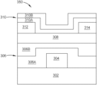
- FIGS. 3 A- 3 B are a schematic, cross sectional view of thin film transistors (TFT) 300 , 350 , respectively, utilized in a display device, according to various embodiments.
- the TFT 300 of FIG. 3 A and the TFT 350 of FIG. 3 B are the same; however the gate insulating layer 306 of the TFT 300 of FIG. 3 A is a single layer while the gate insulating layer 306 of the TFT 350 of FIG. 3 B is a dual layer, and the passivation layer 310 of the TFT 300 of FIG. 3 A is a single layer while the passivation layer 310 of the TFT 350 of FIG. 3 B is a dual layer.
- the 3 B each comprise a substrate 302 .
- the substrate 302 may be made of a silicon-containing material, glass, polyimide, or plastic, such as PET or PEN.
- a gate electrode 304 is disposed on the substrate 302 .
- the gate electrode 304 may comprise copper, tungsten, tantalum, aluminum, among others.
- a gate insulating layer 306 is disposed over the gate electrode 304 and the substrate 302 .
- a semiconductor layer 308 is disposed over the gate insulating layer 306 .
- the semiconductor layer 308 may comprise a metal oxide semiconductor material, a metal oxynitride semiconductor material, such as indium gallium zinc oxide (IGZO), or silicon, such as amorphous silicon, crystalline silicon, and polysilicon, among others.
- a drain electrode 312 and a source electrode 314 are disposed on the semiconductor layer 308 .
- the drain electrode 312 is spaced from and adjacent to the source electrode 314 .
- the drain electrode 312 and the source electrode 314 may each comprise copper, tungsten, tantalum, aluminum, among others.
- a passivation layer 310 is disposed over the semiconductor layer 308 , the drain electrode 312 , and the source electrode 314 .
- the passivation layer 310 and the gate insulating layer 306 are moisture barrier films or layers.
- the passivation layer 310 and the gate insulating layer 306 may each individually comprise the same material as the first barrier layer 208 of FIG. 2 .
- the passivation layer 310 and/or the gate insulating layer 306 are at least partially comprised of a material comprising silicon oxynitride (SiON).
- the SiON material of the passivation layer 310 and/or the gate insulating layer 306 has a refractive index at 632 nm of less than about 1.5, such as about 1.46 to about 1.48, and a WVTR of less than about 5.0 ⁇ 10 ⁇ 5 g/m 2 /day at 40 degrees Celsius and a relative humidity of 100%.
- the SiON material of the passivation layer 310 and/or the gate insulating layer 306 has a composition by XPS of about 1.70 to about 2.15 of O/Si and about 0.01 to about 0.05 of N/Si.
- the SiON material of the passivation layer 310 and/or the gate insulating layer 306 further has a density by XPS of about 2.15 g/cm 3 to about 2.20 g/cm 3 .
- the SiON material of the passivation layer 310 and/or the gate insulating layer 306 has a Si—O—Si peak position of about 1050 cm ⁇ 1 to about 1080 cm ⁇ 1 when measured by FTIR. Additionally, the SiON material of the passivation layer 310 and/or the gate insulating layer 306 has a thickness change percentage of about 104% to about 106% at 85 degrees Celsius and a relative humidity of 85% (i.e., saturated).
- the SiON material of the passivation layer 310 and/or the gate insulating layer 306 has a composition by HFS of hydrogen of about less than 8%. In one embodiment, the SiON material of the passivation layer 310 has a composition by HFS of hydrogen of about less than 6%, and the SiON material of the gate insulating layer 306 has a composition by HFS of hydrogen of about less than 5%.
- the passivation layer 310 and the gate insulating layer 306 may each comprise the SiON material having the above described properties and composition, or only one of the passivation layer 310 or the gate insulating layer 306 may comprise the SiON material having the above described properties and composition,
- FIG. 3 A illustrates a single layer gate insulating layer 306 and a single layer passivation layer 310 .
- the single layer gate insulating layer 306 and the single layer passivation layer 310 may each individually comprise SiON.
- FIG. 3 B illustrates a dual layer gate insulating layer 306 and a dual layer passivation layer 310 .
- the gate insulating layer 306 comprises a layer comprising SiON 306 A and a layer comprising silicon oxide (SiOx) 306 B.
- the layer comprising SiON 306 A of the gate insulating layer 306 is disposed on and in contact with the substrate 302 and the gate electrode 304 .
- the passivation layer 310 and the gate insulating layer 306 may be formed by the same PECVD process as the first barrier layer 208 of FIG. 2 .
- the passivation layer 310 and the gate insulating layer 306 may be formed by a CVD or ALD process.
- the PECVD process for depositing the passivation layer 310 and/or the gate insulating layer 306 may include introducing a silicon-containing precursor and a nitrogen containing precursor into a PECVD chamber, such as the chamber 100 of FIG. 1 .
- the passivation layer 310 is deposited at a temperature of less than about 300 degrees Celsius and the gate insulating layer 306 is deposited at a temperature of less than about 100 degrees Celsius.
- the passivation layer 310 and the gate insulating layer 306 are each SiON, and SiH 4 , N 2 O, NH 3 , N 2 , and H 2 gases are introduced into the chamber for depositing the SiON passivation layer 310 and the SiON gate insulating layer 306 .
- the gate insulating layer 306 is deposited first, followed by the semiconductor layer 308 , followed by the passivation layer 310 .
- the chamber may be purged between each layer deposition.
- the flow rate ratio of the NH 3 gas to the SiH 4 gas ranges from about 0.9 to 1.1
- the flow rate ratio of the N 2 O gas to the SiH 4 gas ranges from about 15.5 to 16.5
- the flow rate ratio of the N 2 gas to the SiH 4 gas ranges from about 8.4 to 8.5
- the flow rate ratio of the H 2 gas to the total flow ratio ranges from about 0.13 to 0.16
- the flow rate ratio of the N 2 O gas to the total flow ratio ranges from about 0.23 to 0.36.
- the chamber pressure ranges from about 0.13 Torr to about 0.14 Torr
- a power density ranges from about 4.5 mW/mm 2 to about 6.5 mW/mm 2 .
- the passivation layer 310 and/or the gate insulating layer 306 having the above mentioned properties reduce the optical loss by about 10% as compared to silicon nitride films and help prevent moisture and/or hydrogen diffusion from occurring within the display devices, further preventing the characteristics of the TFTs 300 , 350 from shifting undesirably.
- the passivation layer 310 and/or the gate insulating layer 306 having a low refractive index of less than about 1.5, a low WVTR of less than about 5.0 ⁇ 10 ⁇ 5 g/m 2 /day, and low H 2 content of less than about 8% results in less change in positive bias temperature stress, negative bias temperature stress, and negative bias temperature illumination stress.
- the passivation layer 310 and/or the gate insulating layer 306 having the above mentioned properties enable better bias stability and lower turn-on voltages when integrated into the TFTs 300 , 350 .
- a moisture barrier film as a first barrier layer in a TFE or as a passivation layer and/or a gate insulating layer in a TFT comprising SiON having a low refractive index of less than about 1.5, a low WVTR of less than about 5.0 ⁇ 10 ⁇ 5 g/m 2 /day, and low H 2 content of less than about 8% enables the layers to be reliable barrier layers in transparent or flexible display devices that are moisture sensitive, H bond sensitive, and/or OH bond sensitive devices.
- the moisture barrier layers each having the above mentioned properties reduce the optical loss by about 10% as compared to silicon nitride films and help prevent moisture and/or hydrogen diffusion from occurring within the display devices, further preventing TFEs from failing and preventing the characteristics of TFTs from shifting undesirably.
Landscapes
- Physics & Mathematics (AREA)
- Engineering & Computer Science (AREA)
- Optics & Photonics (AREA)
- Microelectronics & Electronic Packaging (AREA)
- Chemical & Material Sciences (AREA)
- Inorganic Chemistry (AREA)
- Geometry (AREA)
- Manufacturing & Machinery (AREA)
- Electroluminescent Light Sources (AREA)
- Chemical Vapour Deposition (AREA)
- Formation Of Insulating Films (AREA)
- Thin Film Transistor (AREA)
- Liquid Crystal (AREA)
Priority Applications (1)
| Application Number | Priority Date | Filing Date | Title |
|---|---|---|---|
| US17/604,503 US12317543B2 (en) | 2019-04-25 | 2019-07-10 | Moisture barrier film having low refraction index and low water vapor transmission rate |
Applications Claiming Priority (3)
| Application Number | Priority Date | Filing Date | Title |
|---|---|---|---|
| US201962838883P | 2019-04-25 | 2019-04-25 | |
| US17/604,503 US12317543B2 (en) | 2019-04-25 | 2019-07-10 | Moisture barrier film having low refraction index and low water vapor transmission rate |
| PCT/US2019/041163 WO2020219087A1 (en) | 2019-04-25 | 2019-07-10 | Moisture barrier film having low refraction index and low water vapor tramission rate |
Publications (2)
| Publication Number | Publication Date |
|---|---|
| US20220209188A1 US20220209188A1 (en) | 2022-06-30 |
| US12317543B2 true US12317543B2 (en) | 2025-05-27 |
Family
ID=72941218
Family Applications (1)
| Application Number | Title | Priority Date | Filing Date |
|---|---|---|---|
| US17/604,503 Active 2041-08-07 US12317543B2 (en) | 2019-04-25 | 2019-07-10 | Moisture barrier film having low refraction index and low water vapor transmission rate |
Country Status (6)
| Country | Link |
|---|---|
| US (1) | US12317543B2 (zh) |
| JP (1) | JP7304966B2 (zh) |
| KR (2) | KR102766447B1 (zh) |
| CN (2) | CN118251042A (zh) |
| TW (2) | TWI754223B (zh) |
| WO (1) | WO2020219087A1 (zh) |
Citations (36)
| Publication number | Priority date | Publication date | Assignee | Title |
|---|---|---|---|---|
| JPH07211712A (ja) | 1994-01-25 | 1995-08-11 | Canon Sales Co Inc | 成膜方法 |
| US20030143319A1 (en) | 2002-01-25 | 2003-07-31 | Park Sang Hee | Flat panel display device and method of forming passivation film in the flat panel display device |
| US20110097533A1 (en) | 2009-10-27 | 2011-04-28 | Suna Displays Co., Ltd. | Thin film encapsulation method |
| JP2011258943A (ja) | 2010-05-14 | 2011-12-22 | Semiconductor Energy Lab Co Ltd | 薄膜の作製方法、およびトランジスタの作製方法 |
| JP2013232279A (ja) | 2010-07-27 | 2013-11-14 | Hitachi Ltd | 封止膜およびそれを用いた有機発光ダイオード |
| US20130334511A1 (en) | 2012-06-13 | 2013-12-19 | Plasmasi, Inc. | Method for deposition of high-performance coatings and encapsulated electronic devices |
| TW201417224A (zh) | 2012-10-22 | 2014-05-01 | Ind Tech Res Inst | 可撓式電子裝置及其製造方法 |
| US20140246655A1 (en) | 2013-03-04 | 2014-09-04 | Applied Materials, Inc. | Fluorine-containing plasma polymerized hmdso for oled thin film encapsulation |
| US20140256070A1 (en) | 2013-03-11 | 2014-09-11 | Applied Materials, Inc. | Plasma curing of pecvd hmdso film for oled applications |
| US20140306218A1 (en) * | 2013-04-11 | 2014-10-16 | Junichi Koezuka | Display device and electronic device |
| CN104115300A (zh) | 2012-02-15 | 2014-10-22 | 应用材料公司 | 沉积包封膜的方法 |
| US8906813B2 (en) | 2012-05-10 | 2014-12-09 | Applied Materials, Inc. | SiOx process chemistry development using microwave plasma CVD |
| JP2015024536A (ja) | 2013-07-25 | 2015-02-05 | コニカミノルタ株式会社 | ガスバリアー性フィルムの製造方法 |
| US20150084035A1 (en) | 2013-09-23 | 2015-03-26 | Samsung Display Co., Ltd. | Thin film transistor and method of manufacturing the same |
| CN104584256A (zh) | 2012-09-04 | 2015-04-29 | 应用材料公司 | 用于有机发光二极管的混合封装的方法 |
| TW201523867A (zh) | 2013-12-10 | 2015-06-16 | Au Optronics Corp | 顯示面板及其製作方法 |
| KR20150126558A (ko) | 2014-05-02 | 2015-11-12 | 가부시키가이샤 한도오따이 에네루기 켄큐쇼 | 반도체 장치, 터치 센서, 표시 장치 |
| CN105190932A (zh) | 2013-03-12 | 2015-12-23 | 应用材料公司 | 用于薄膜封装的n2o稀释工艺对阻挡膜性能的改进 |
| US20150368801A1 (en) | 2014-06-18 | 2015-12-24 | Applied Materials, Inc. | Plasma process chambers employing distribution grids having focusing surfaces thereon enabling angled fluxes to reach a substrate, and related methods |
| TW201609428A (zh) | 2014-07-31 | 2016-03-16 | 羅利克股份公司 | 用於倂有抗反射性質之oled顯示器的封裝結構 |
| US9293706B2 (en) | 2011-02-07 | 2016-03-22 | Applied Materials, Inc. | Method for encapsulating an organic light emitting diode |
| US9337051B2 (en) | 2014-08-14 | 2016-05-10 | Applied Materials, Inc. | Method for critical dimension reduction using conformal carbon films |
| US20160190511A1 (en) | 2014-12-30 | 2016-06-30 | Samsung Display Co., Ltd. | Organic light-emitting display apparatus and method of manufacturing the same |
| TW201628230A (zh) | 2015-01-22 | 2016-08-01 | 財團法人工業技術研究院 | 可撓性環境敏感電子元件封裝 |
| CN105826485A (zh) | 2015-01-22 | 2016-08-03 | 财团法人工业技术研究院 | 可挠性环境敏感电子元件封装 |
| US9478421B2 (en) | 2013-05-03 | 2016-10-25 | Applied Materials, Inc. | Optically tuned hardmask for multi-patterning applications |
| US20160336542A1 (en) * | 2015-05-14 | 2016-11-17 | Applied Materials, Inc. | Encapsulating film stacks for oled applications |
| US20170104048A1 (en) | 2015-10-13 | 2017-04-13 | Samsung Display Co., Ltd. | Substrate structure |
| KR20180003287A (ko) | 2016-06-30 | 2018-01-09 | 엘지디스플레이 주식회사 | 유기 발광 표시 장치 |
| CN107636793A (zh) | 2015-03-17 | 2018-01-26 | 应用材料公司 | 离子对离子等离子体原子层蚀刻工艺及反应器 |
| TW201810762A (zh) | 2016-09-14 | 2018-03-16 | 財團法人工業技術研究院 | 可撓性有機發光二極體的結構及其製造方法 |
| WO2018130288A1 (en) | 2017-01-12 | 2018-07-19 | Applied Materials, Inc. | Barrier layer system and method for manufacturing a barrier layer system in a continuous roll-to-roll process |
| JP6442117B1 (ja) | 2018-01-31 | 2018-12-19 | 堺ディスプレイプロダクト株式会社 | 有機el表示装置の製造方法 |
| KR101942042B1 (ko) | 2016-08-05 | 2019-01-25 | 마븐 옵트로닉스 씨오., 엘티디. | 내습성 칩 스케일 패키징 발광 디바이스 |
| US20190097175A1 (en) | 2017-09-28 | 2019-03-28 | Applied Materials, Inc. | Thin film encapsulation scattering layer by pecvd |
| US20190371918A1 (en) * | 2018-05-30 | 2019-12-05 | Globalfoundries Inc. | Mitigation of hot carrier damage in field-effect transistors |
Family Cites Families (7)
| Publication number | Priority date | Publication date | Assignee | Title |
|---|---|---|---|---|
| TWI345307B (en) * | 2007-02-16 | 2011-07-11 | Chi Mei El Corp | Display device and method of manufacturing the same |
| TWI348767B (en) * | 2007-12-07 | 2011-09-11 | Chimei Innolux Corp | Thin film transistor and manufacture method thereof |
| TWI559510B (zh) * | 2014-06-23 | 2016-11-21 | 群創光電股份有限公司 | 顯示裝置 |
| KR102516054B1 (ko) * | 2015-11-13 | 2023-03-31 | 삼성디스플레이 주식회사 | 유기발광표시장치 및 유기발광표시장치의 제조 방법 |
| KR102867300B1 (ko) * | 2016-10-31 | 2025-10-01 | 엘지디스플레이 주식회사 | 유기 발광 표시 장치 |
| KR102854033B1 (ko) * | 2016-11-30 | 2025-09-02 | 엘지디스플레이 주식회사 | 유기 발광 표시 장치 |
| KR102382487B1 (ko) * | 2017-09-15 | 2022-04-01 | 엘지디스플레이 주식회사 | 유기발광 다이오드 표시장치 |
-
2019
- 2019-07-10 US US17/604,503 patent/US12317543B2/en active Active
- 2019-07-10 CN CN202410415312.2A patent/CN118251042A/zh active Pending
- 2019-07-10 WO PCT/US2019/041163 patent/WO2020219087A1/en not_active Ceased
- 2019-07-10 KR KR1020217038267A patent/KR102766447B1/ko active Active
- 2019-07-10 CN CN201980094735.6A patent/CN113841263B/zh active Active
- 2019-07-10 JP JP2021562325A patent/JP7304966B2/ja active Active
- 2019-07-10 KR KR1020257003677A patent/KR20250022257A/ko active Pending
-
2020
- 2020-02-15 TW TW109104879A patent/TWI754223B/zh active
- 2020-02-15 TW TW110149730A patent/TWI809637B/zh active
Patent Citations (39)
| Publication number | Priority date | Publication date | Assignee | Title |
|---|---|---|---|---|
| US5554570A (en) | 1994-01-25 | 1996-09-10 | Canon Sales Co., Inc. | Method of forming insulating film |
| JPH07211712A (ja) | 1994-01-25 | 1995-08-11 | Canon Sales Co Inc | 成膜方法 |
| US20030143319A1 (en) | 2002-01-25 | 2003-07-31 | Park Sang Hee | Flat panel display device and method of forming passivation film in the flat panel display device |
| US20110097533A1 (en) | 2009-10-27 | 2011-04-28 | Suna Displays Co., Ltd. | Thin film encapsulation method |
| JP2011258943A (ja) | 2010-05-14 | 2011-12-22 | Semiconductor Energy Lab Co Ltd | 薄膜の作製方法、およびトランジスタの作製方法 |
| JP2013232279A (ja) | 2010-07-27 | 2013-11-14 | Hitachi Ltd | 封止膜およびそれを用いた有機発光ダイオード |
| US9293706B2 (en) | 2011-02-07 | 2016-03-22 | Applied Materials, Inc. | Method for encapsulating an organic light emitting diode |
| CN104115300A (zh) | 2012-02-15 | 2014-10-22 | 应用材料公司 | 沉积包封膜的方法 |
| US8906813B2 (en) | 2012-05-10 | 2014-12-09 | Applied Materials, Inc. | SiOx process chemistry development using microwave plasma CVD |
| US20130334511A1 (en) | 2012-06-13 | 2013-12-19 | Plasmasi, Inc. | Method for deposition of high-performance coatings and encapsulated electronic devices |
| CN104584256A (zh) | 2012-09-04 | 2015-04-29 | 应用材料公司 | 用于有机发光二极管的混合封装的方法 |
| TW201417224A (zh) | 2012-10-22 | 2014-05-01 | Ind Tech Res Inst | 可撓式電子裝置及其製造方法 |
| US20140246655A1 (en) | 2013-03-04 | 2014-09-04 | Applied Materials, Inc. | Fluorine-containing plasma polymerized hmdso for oled thin film encapsulation |
| US20140256070A1 (en) | 2013-03-11 | 2014-09-11 | Applied Materials, Inc. | Plasma curing of pecvd hmdso film for oled applications |
| CN105190932A (zh) | 2013-03-12 | 2015-12-23 | 应用材料公司 | 用于薄膜封装的n2o稀释工艺对阻挡膜性能的改进 |
| US20140306218A1 (en) * | 2013-04-11 | 2014-10-16 | Junichi Koezuka | Display device and electronic device |
| US9478421B2 (en) | 2013-05-03 | 2016-10-25 | Applied Materials, Inc. | Optically tuned hardmask for multi-patterning applications |
| JP2015024536A (ja) | 2013-07-25 | 2015-02-05 | コニカミノルタ株式会社 | ガスバリアー性フィルムの製造方法 |
| US20150084035A1 (en) | 2013-09-23 | 2015-03-26 | Samsung Display Co., Ltd. | Thin film transistor and method of manufacturing the same |
| TW201523867A (zh) | 2013-12-10 | 2015-06-16 | Au Optronics Corp | 顯示面板及其製作方法 |
| KR20150126558A (ko) | 2014-05-02 | 2015-11-12 | 가부시키가이샤 한도오따이 에네루기 켄큐쇼 | 반도체 장치, 터치 센서, 표시 장치 |
| JP2015228491A (ja) | 2014-05-02 | 2015-12-17 | 株式会社半導体エネルギー研究所 | 半導体装置、タッチセンサ、表示装置 |
| US20150368801A1 (en) | 2014-06-18 | 2015-12-24 | Applied Materials, Inc. | Plasma process chambers employing distribution grids having focusing surfaces thereon enabling angled fluxes to reach a substrate, and related methods |
| TW201609428A (zh) | 2014-07-31 | 2016-03-16 | 羅利克股份公司 | 用於倂有抗反射性質之oled顯示器的封裝結構 |
| US9337051B2 (en) | 2014-08-14 | 2016-05-10 | Applied Materials, Inc. | Method for critical dimension reduction using conformal carbon films |
| US20160190511A1 (en) | 2014-12-30 | 2016-06-30 | Samsung Display Co., Ltd. | Organic light-emitting display apparatus and method of manufacturing the same |
| TW201628230A (zh) | 2015-01-22 | 2016-08-01 | 財團法人工業技術研究院 | 可撓性環境敏感電子元件封裝 |
| CN105826485A (zh) | 2015-01-22 | 2016-08-03 | 财团法人工业技术研究院 | 可挠性环境敏感电子元件封装 |
| CN107636793A (zh) | 2015-03-17 | 2018-01-26 | 应用材料公司 | 离子对离子等离子体原子层蚀刻工艺及反应器 |
| US20160336542A1 (en) * | 2015-05-14 | 2016-11-17 | Applied Materials, Inc. | Encapsulating film stacks for oled applications |
| US20170104048A1 (en) | 2015-10-13 | 2017-04-13 | Samsung Display Co., Ltd. | Substrate structure |
| KR20170043726A (ko) | 2015-10-13 | 2017-04-24 | 삼성디스플레이 주식회사 | 투명 표시 기판 및 투명 표시 장치 |
| KR20180003287A (ko) | 2016-06-30 | 2018-01-09 | 엘지디스플레이 주식회사 | 유기 발광 표시 장치 |
| KR101942042B1 (ko) | 2016-08-05 | 2019-01-25 | 마븐 옵트로닉스 씨오., 엘티디. | 내습성 칩 스케일 패키징 발광 디바이스 |
| TW201810762A (zh) | 2016-09-14 | 2018-03-16 | 財團法人工業技術研究院 | 可撓性有機發光二極體的結構及其製造方法 |
| WO2018130288A1 (en) | 2017-01-12 | 2018-07-19 | Applied Materials, Inc. | Barrier layer system and method for manufacturing a barrier layer system in a continuous roll-to-roll process |
| US20190097175A1 (en) | 2017-09-28 | 2019-03-28 | Applied Materials, Inc. | Thin film encapsulation scattering layer by pecvd |
| JP6442117B1 (ja) | 2018-01-31 | 2018-12-19 | 堺ディスプレイプロダクト株式会社 | 有機el表示装置の製造方法 |
| US20190371918A1 (en) * | 2018-05-30 | 2019-12-05 | Globalfoundries Inc. | Mitigation of hot carrier damage in field-effect transistors |
Non-Patent Citations (8)
| Title |
|---|
| Chinese Office Action dated Aug. 25, 2023; CN patent application No. 2019800947356. |
| Chinese Office Action Dated May 10, 2024 re: Chinese Application No. 201980083749.8. |
| International Search Report and Written Opinion in related application PCT/US2019/041163 dated Jan. 22, 2020. |
| Japanese Office Action dated Feb. 14, 2023 for Application No. 2021-562325. |
| Japanese Office Action Dated Feb. 21, 2023 for Application No. 2021-540804. |
| Korean Office Action dated Apr. 9, 2024 for Application No. 10-2021-7038267. |
| Serényi et al. "Refractive index of sputtered silicon oxynitride layers for antireflection coating," Vacuum, 2001, vol. 61, No. 2-4, pp. 245-249, DOI: 10.1016/S0042-207X(01)00124-5. |
| Taiwanese Notice of Allowance and Issue Fee for Application No. 110149730. |
Also Published As
| Publication number | Publication date |
|---|---|
| TWI809637B (zh) | 2023-07-21 |
| KR20250022257A (ko) | 2025-02-14 |
| CN113841263B (zh) | 2024-04-26 |
| TW202040841A (zh) | 2020-11-01 |
| CN118251042A (zh) | 2024-06-25 |
| TW202232769A (zh) | 2022-08-16 |
| CN113841263A (zh) | 2021-12-24 |
| JP2022530379A (ja) | 2022-06-29 |
| KR20210143951A (ko) | 2021-11-29 |
| WO2020219087A1 (en) | 2020-10-29 |
| TWI754223B (zh) | 2022-02-01 |
| US20220209188A1 (en) | 2022-06-30 |
| JP7304966B2 (ja) | 2023-07-07 |
| KR102766447B1 (ko) | 2025-02-10 |
Similar Documents
| Publication | Publication Date | Title |
|---|---|---|
| CN102113120B (zh) | 用于薄膜晶体管的杂化的介电材料 | |
| US9935183B2 (en) | Multilayer passivation or etch stop TFT | |
| US8012794B2 (en) | Capping layers for metal oxynitride TFTS | |
| US9269923B2 (en) | Barrier films for thin film encapsulation | |
| US20110068332A1 (en) | Hybrid Dielectric Material for Thin Film Transistors | |
| KR102208520B1 (ko) | 디스플레이 디바이스들에서 활용되는 지르코늄 산화물을 포함하는 하이-k 유전체 재료들 | |
| US10658400B2 (en) | Method of manufacturing display device having a multilayered undercoating layer of silicon oxide and silicon nitride | |
| US12317543B2 (en) | Moisture barrier film having low refraction index and low water vapor transmission rate | |
| US20190097175A1 (en) | Thin film encapsulation scattering layer by pecvd | |
| TWI613820B (zh) | 用於tft之金屬氧化物半導體之緩衝層 | |
| KR20180118958A (ko) | 박막 트랜지스터 및 그 제조 방법 | |
| KR102808971B1 (ko) | 디스플레이 캡슐화 애플리케이션을 위한 고밀도 플라즈마 cvd |
Legal Events
| Date | Code | Title | Description |
|---|---|---|---|
| FEPP | Fee payment procedure |
Free format text: ENTITY STATUS SET TO UNDISCOUNTED (ORIGINAL EVENT CODE: BIG.); ENTITY STATUS OF PATENT OWNER: LARGE ENTITY |
|
| AS | Assignment |
Owner name: APPLIED MATERIALS, INC., CALIFORNIA Free format text: ASSIGNMENT OF ASSIGNORS INTEREST;ASSIGNORS:WU, WEN-HAO;CHEN, JRIYAN JERRY;YIM, DONG KIL;REEL/FRAME:057995/0946 Effective date: 20211013 |
|
| STPP | Information on status: patent application and granting procedure in general |
Free format text: DOCKETED NEW CASE - READY FOR EXAMINATION |
|
| STPP | Information on status: patent application and granting procedure in general |
Free format text: NON FINAL ACTION MAILED |
|
| STPP | Information on status: patent application and granting procedure in general |
Free format text: RESPONSE TO NON-FINAL OFFICE ACTION ENTERED AND FORWARDED TO EXAMINER |
|
| STPP | Information on status: patent application and granting procedure in general |
Free format text: FINAL REJECTION MAILED |
|
| STCF | Information on status: patent grant |
Free format text: PATENTED CASE |