US11387371B2 - Thin film transistor and manufacturing method thereof and electronic device - Google Patents
Thin film transistor and manufacturing method thereof and electronic device Download PDFInfo
- Publication number
- US11387371B2 US11387371B2 US16/330,255 US201816330255A US11387371B2 US 11387371 B2 US11387371 B2 US 11387371B2 US 201816330255 A US201816330255 A US 201816330255A US 11387371 B2 US11387371 B2 US 11387371B2
- Authority
- US
- United States
- Prior art keywords
- layer
- work function
- auxiliary layer
- gate electrode
- thin film
- Prior art date
- Legal status (The legal status is an assumption and is not a legal conclusion. Google has not performed a legal analysis and makes no representation as to the accuracy of the status listed.)
- Active, expires
Links
- 239000010409 thin film Substances 0.000 title claims abstract description 104
- 238000004519 manufacturing process Methods 0.000 title claims description 14
- 239000000758 substrate Substances 0.000 claims abstract description 80
- 239000000463 material Substances 0.000 claims description 194
- BASFCYQUMIYNBI-UHFFFAOYSA-N platinum Chemical group [Pt] BASFCYQUMIYNBI-UHFFFAOYSA-N 0.000 claims description 24
- 239000004065 semiconductor Substances 0.000 claims description 23
- KDLHZDBZIXYQEI-UHFFFAOYSA-N Palladium Chemical compound [Pd] KDLHZDBZIXYQEI-UHFFFAOYSA-N 0.000 claims description 12
- ZOKXTWBITQBERF-UHFFFAOYSA-N Molybdenum Chemical compound [Mo] ZOKXTWBITQBERF-UHFFFAOYSA-N 0.000 claims description 11
- 229910052750 molybdenum Inorganic materials 0.000 claims description 11
- 239000011733 molybdenum Substances 0.000 claims description 11
- 239000004020 conductor Substances 0.000 claims description 10
- 229910052697 platinum Inorganic materials 0.000 claims description 10
- 229910044991 metal oxide Inorganic materials 0.000 claims description 9
- 150000004706 metal oxides Chemical class 0.000 claims description 9
- 239000004973 liquid crystal related substance Substances 0.000 claims description 8
- RYGMFSIKBFXOCR-UHFFFAOYSA-N Copper Chemical group [Cu] RYGMFSIKBFXOCR-UHFFFAOYSA-N 0.000 claims description 7
- RTAQQCXQSZGOHL-UHFFFAOYSA-N Titanium Chemical compound [Ti] RTAQQCXQSZGOHL-UHFFFAOYSA-N 0.000 claims description 7
- 229910052782 aluminium Inorganic materials 0.000 claims description 7
- XAGFODPZIPBFFR-UHFFFAOYSA-N aluminium Chemical compound [Al] XAGFODPZIPBFFR-UHFFFAOYSA-N 0.000 claims description 7
- 229910052802 copper Inorganic materials 0.000 claims description 7
- 239000010949 copper Substances 0.000 claims description 7
- 229910052710 silicon Inorganic materials 0.000 claims description 7
- 239000010703 silicon Substances 0.000 claims description 7
- 229910052719 titanium Inorganic materials 0.000 claims description 7
- 239000010936 titanium Substances 0.000 claims description 7
- PCHJSUWPFVWCPO-UHFFFAOYSA-N gold Chemical compound [Au] PCHJSUWPFVWCPO-UHFFFAOYSA-N 0.000 claims description 6
- 229910052737 gold Inorganic materials 0.000 claims description 6
- 239000010931 gold Substances 0.000 claims description 6
- 229910052763 palladium Inorganic materials 0.000 claims description 6
- 241000206607 Porphyra umbilicalis Species 0.000 claims 1
- XUIMIQQOPSSXEZ-UHFFFAOYSA-N Silicon Chemical compound [Si] XUIMIQQOPSSXEZ-UHFFFAOYSA-N 0.000 claims 1
- 239000007772 electrode material Substances 0.000 description 32
- 229920005591 polysilicon Polymers 0.000 description 28
- 229910021420 polycrystalline silicon Inorganic materials 0.000 description 25
- 238000000034 method Methods 0.000 description 22
- 239000007769 metal material Substances 0.000 description 10
- 238000000059 patterning Methods 0.000 description 10
- 239000003990 capacitor Substances 0.000 description 7
- 230000000694 effects Effects 0.000 description 6
- AMGQUBHHOARCQH-UHFFFAOYSA-N indium;oxotin Chemical compound [In].[Sn]=O AMGQUBHHOARCQH-UHFFFAOYSA-N 0.000 description 5
- 229920002120 photoresistant polymer Polymers 0.000 description 5
- WFKWXMTUELFFGS-UHFFFAOYSA-N tungsten Chemical compound [W] WFKWXMTUELFFGS-UHFFFAOYSA-N 0.000 description 5
- 229910052721 tungsten Inorganic materials 0.000 description 5
- 239000010937 tungsten Substances 0.000 description 5
- 239000004642 Polyimide Substances 0.000 description 4
- XLOMVQKBTHCTTD-UHFFFAOYSA-N Zinc monoxide Chemical compound [Zn]=O XLOMVQKBTHCTTD-UHFFFAOYSA-N 0.000 description 4
- 239000000203 mixture Substances 0.000 description 4
- 229920000139 polyethylene terephthalate Polymers 0.000 description 4
- 239000005020 polyethylene terephthalate Substances 0.000 description 4
- 229920001721 polyimide Polymers 0.000 description 4
- 229920012266 Poly(ether sulfone) PES Polymers 0.000 description 2
- 230000015572 biosynthetic process Effects 0.000 description 2
- 238000005137 deposition process Methods 0.000 description 2
- 238000005530 etching Methods 0.000 description 2
- 239000010408 film Substances 0.000 description 2
- 239000011521 glass Substances 0.000 description 2
- 239000002985 plastic film Substances 0.000 description 2
- 229920006255 plastic film Polymers 0.000 description 2
- 239000004417 polycarbonate Substances 0.000 description 2
- 229920000515 polycarbonate Polymers 0.000 description 2
- -1 polyethylene terephthalate Polymers 0.000 description 2
- 239000010935 stainless steel Substances 0.000 description 2
- 229910001220 stainless steel Inorganic materials 0.000 description 2
- 239000011787 zinc oxide Substances 0.000 description 2
- GYHNNYVSQQEPJS-UHFFFAOYSA-N Gallium Chemical compound [Ga] GYHNNYVSQQEPJS-UHFFFAOYSA-N 0.000 description 1
- 229910045601 alloy Inorganic materials 0.000 description 1
- 239000000956 alloy Substances 0.000 description 1
- 229910021417 amorphous silicon Inorganic materials 0.000 description 1
- 238000010586 diagram Methods 0.000 description 1
- 230000005684 electric field Effects 0.000 description 1
- 229910052733 gallium Inorganic materials 0.000 description 1
- 239000012535 impurity Substances 0.000 description 1
- 229910052738 indium Inorganic materials 0.000 description 1
- APFVFJFRJDLVQX-UHFFFAOYSA-N indium atom Chemical compound [In] APFVFJFRJDLVQX-UHFFFAOYSA-N 0.000 description 1
- 239000011159 matrix material Substances 0.000 description 1
- 230000008054 signal transmission Effects 0.000 description 1
- 238000002834 transmittance Methods 0.000 description 1
Images


Classifications
-
- H—ELECTRICITY
- H01—ELECTRIC ELEMENTS
- H01L—SEMICONDUCTOR DEVICES NOT COVERED BY CLASS H10
- H01L29/00—Semiconductor devices specially adapted for rectifying, amplifying, oscillating or switching and having potential barriers; Capacitors or resistors having potential barriers, e.g. a PN-junction depletion layer or carrier concentration layer; Details of semiconductor bodies or of electrodes thereof ; Multistep manufacturing processes therefor
- H01L29/66—Types of semiconductor device ; Multistep manufacturing processes therefor
- H01L29/68—Types of semiconductor device ; Multistep manufacturing processes therefor controllable by only the electric current supplied, or only the electric potential applied, to an electrode which does not carry the current to be rectified, amplified or switched
- H01L29/76—Unipolar devices, e.g. field effect transistors
- H01L29/772—Field effect transistors
- H01L29/78—Field effect transistors with field effect produced by an insulated gate
- H01L29/786—Thin film transistors, i.e. transistors with a channel being at least partly a thin film
- H01L29/78651—Silicon transistors
- H01L29/7866—Non-monocrystalline silicon transistors
- H01L29/78672—Polycrystalline or microcrystalline silicon transistor
- H01L29/78678—Polycrystalline or microcrystalline silicon transistor with inverted-type structure, e.g. with bottom gate
-
- H—ELECTRICITY
- H01—ELECTRIC ELEMENTS
- H01L—SEMICONDUCTOR DEVICES NOT COVERED BY CLASS H10
- H01L29/00—Semiconductor devices specially adapted for rectifying, amplifying, oscillating or switching and having potential barriers; Capacitors or resistors having potential barriers, e.g. a PN-junction depletion layer or carrier concentration layer; Details of semiconductor bodies or of electrodes thereof ; Multistep manufacturing processes therefor
- H01L29/40—Electrodes ; Multistep manufacturing processes therefor
- H01L29/41—Electrodes ; Multistep manufacturing processes therefor characterised by their shape, relative sizes or dispositions
- H01L29/423—Electrodes ; Multistep manufacturing processes therefor characterised by their shape, relative sizes or dispositions not carrying the current to be rectified, amplified or switched
- H01L29/42312—Gate electrodes for field effect devices
- H01L29/42316—Gate electrodes for field effect devices for field-effect transistors
- H01L29/4232—Gate electrodes for field effect devices for field-effect transistors with insulated gate
- H01L29/42384—Gate electrodes for field effect devices for field-effect transistors with insulated gate for thin film field effect transistors, e.g. characterised by the thickness or the shape of the insulator or the dimensions, the shape or the lay-out of the conductor
-
- H—ELECTRICITY
- H01—ELECTRIC ELEMENTS
- H01L—SEMICONDUCTOR DEVICES NOT COVERED BY CLASS H10
- H01L27/00—Devices consisting of a plurality of semiconductor or other solid-state components formed in or on a common substrate
- H01L27/02—Devices consisting of a plurality of semiconductor or other solid-state components formed in or on a common substrate including semiconductor components specially adapted for rectifying, oscillating, amplifying or switching and having potential barriers; including integrated passive circuit elements having potential barriers
- H01L27/12—Devices consisting of a plurality of semiconductor or other solid-state components formed in or on a common substrate including semiconductor components specially adapted for rectifying, oscillating, amplifying or switching and having potential barriers; including integrated passive circuit elements having potential barriers the substrate being other than a semiconductor body, e.g. an insulating body
- H01L27/1214—Devices consisting of a plurality of semiconductor or other solid-state components formed in or on a common substrate including semiconductor components specially adapted for rectifying, oscillating, amplifying or switching and having potential barriers; including integrated passive circuit elements having potential barriers the substrate being other than a semiconductor body, e.g. an insulating body comprising a plurality of TFTs formed on a non-semiconducting substrate, e.g. driving circuits for AMLCDs
- H01L27/1222—Devices consisting of a plurality of semiconductor or other solid-state components formed in or on a common substrate including semiconductor components specially adapted for rectifying, oscillating, amplifying or switching and having potential barriers; including integrated passive circuit elements having potential barriers the substrate being other than a semiconductor body, e.g. an insulating body comprising a plurality of TFTs formed on a non-semiconducting substrate, e.g. driving circuits for AMLCDs with a particular composition, shape or crystalline structure of the active layer
-
- H—ELECTRICITY
- H01—ELECTRIC ELEMENTS
- H01L—SEMICONDUCTOR DEVICES NOT COVERED BY CLASS H10
- H01L27/00—Devices consisting of a plurality of semiconductor or other solid-state components formed in or on a common substrate
- H01L27/02—Devices consisting of a plurality of semiconductor or other solid-state components formed in or on a common substrate including semiconductor components specially adapted for rectifying, oscillating, amplifying or switching and having potential barriers; including integrated passive circuit elements having potential barriers
- H01L27/12—Devices consisting of a plurality of semiconductor or other solid-state components formed in or on a common substrate including semiconductor components specially adapted for rectifying, oscillating, amplifying or switching and having potential barriers; including integrated passive circuit elements having potential barriers the substrate being other than a semiconductor body, e.g. an insulating body
- H01L27/1214—Devices consisting of a plurality of semiconductor or other solid-state components formed in or on a common substrate including semiconductor components specially adapted for rectifying, oscillating, amplifying or switching and having potential barriers; including integrated passive circuit elements having potential barriers the substrate being other than a semiconductor body, e.g. an insulating body comprising a plurality of TFTs formed on a non-semiconducting substrate, e.g. driving circuits for AMLCDs
- H01L27/1259—Multistep manufacturing methods
- H01L27/127—Multistep manufacturing methods with a particular formation, treatment or patterning of the active layer specially adapted to the circuit arrangement
-
- H—ELECTRICITY
- H01—ELECTRIC ELEMENTS
- H01L—SEMICONDUCTOR DEVICES NOT COVERED BY CLASS H10
- H01L29/00—Semiconductor devices specially adapted for rectifying, amplifying, oscillating or switching and having potential barriers; Capacitors or resistors having potential barriers, e.g. a PN-junction depletion layer or carrier concentration layer; Details of semiconductor bodies or of electrodes thereof ; Multistep manufacturing processes therefor
- H01L29/40—Electrodes ; Multistep manufacturing processes therefor
- H01L29/41—Electrodes ; Multistep manufacturing processes therefor characterised by their shape, relative sizes or dispositions
-
- H—ELECTRICITY
- H01—ELECTRIC ELEMENTS
- H01L—SEMICONDUCTOR DEVICES NOT COVERED BY CLASS H10
- H01L29/00—Semiconductor devices specially adapted for rectifying, amplifying, oscillating or switching and having potential barriers; Capacitors or resistors having potential barriers, e.g. a PN-junction depletion layer or carrier concentration layer; Details of semiconductor bodies or of electrodes thereof ; Multistep manufacturing processes therefor
- H01L29/40—Electrodes ; Multistep manufacturing processes therefor
- H01L29/43—Electrodes ; Multistep manufacturing processes therefor characterised by the materials of which they are formed
- H01L29/49—Metal-insulator-semiconductor electrodes, e.g. gates of MOSFET
- H01L29/4908—Metal-insulator-semiconductor electrodes, e.g. gates of MOSFET for thin film semiconductor, e.g. gate of TFT
-
- H—ELECTRICITY
- H01—ELECTRIC ELEMENTS
- H01L—SEMICONDUCTOR DEVICES NOT COVERED BY CLASS H10
- H01L29/00—Semiconductor devices specially adapted for rectifying, amplifying, oscillating or switching and having potential barriers; Capacitors or resistors having potential barriers, e.g. a PN-junction depletion layer or carrier concentration layer; Details of semiconductor bodies or of electrodes thereof ; Multistep manufacturing processes therefor
- H01L29/66—Types of semiconductor device ; Multistep manufacturing processes therefor
- H01L29/66007—Multistep manufacturing processes
- H01L29/66075—Multistep manufacturing processes of devices having semiconductor bodies comprising group 14 or group 13/15 materials
- H01L29/66227—Multistep manufacturing processes of devices having semiconductor bodies comprising group 14 or group 13/15 materials the devices being controllable only by the electric current supplied or the electric potential applied, to an electrode which does not carry the current to be rectified, amplified or switched, e.g. three-terminal devices
- H01L29/66409—Unipolar field-effect transistors
- H01L29/66477—Unipolar field-effect transistors with an insulated gate, i.e. MISFET
- H01L29/66742—Thin film unipolar transistors
- H01L29/6675—Amorphous silicon or polysilicon transistors
- H01L29/66765—Lateral single gate single channel transistors with inverted structure, i.e. the channel layer is formed after the gate
-
- H—ELECTRICITY
- H01—ELECTRIC ELEMENTS
- H01L—SEMICONDUCTOR DEVICES NOT COVERED BY CLASS H10
- H01L29/00—Semiconductor devices specially adapted for rectifying, amplifying, oscillating or switching and having potential barriers; Capacitors or resistors having potential barriers, e.g. a PN-junction depletion layer or carrier concentration layer; Details of semiconductor bodies or of electrodes thereof ; Multistep manufacturing processes therefor
- H01L29/66—Types of semiconductor device ; Multistep manufacturing processes therefor
- H01L29/68—Types of semiconductor device ; Multistep manufacturing processes therefor controllable by only the electric current supplied, or only the electric potential applied, to an electrode which does not carry the current to be rectified, amplified or switched
- H01L29/76—Unipolar devices, e.g. field effect transistors
- H01L29/772—Field effect transistors
- H01L29/78—Field effect transistors with field effect produced by an insulated gate
- H01L29/786—Thin film transistors, i.e. transistors with a channel being at least partly a thin film
- H01L29/78696—Thin film transistors, i.e. transistors with a channel being at least partly a thin film characterised by the structure of the channel, e.g. multichannel, transverse or longitudinal shape, length or width, doping structure, or the overlap or alignment between the channel and the gate, the source or the drain, or the contacting structure of the channel
-
- G—PHYSICS
- G02—OPTICS
- G02F—OPTICAL DEVICES OR ARRANGEMENTS FOR THE CONTROL OF LIGHT BY MODIFICATION OF THE OPTICAL PROPERTIES OF THE MEDIA OF THE ELEMENTS INVOLVED THEREIN; NON-LINEAR OPTICS; FREQUENCY-CHANGING OF LIGHT; OPTICAL LOGIC ELEMENTS; OPTICAL ANALOGUE/DIGITAL CONVERTERS
- G02F1/00—Devices or arrangements for the control of the intensity, colour, phase, polarisation or direction of light arriving from an independent light source, e.g. switching, gating or modulating; Non-linear optics
- G02F1/01—Devices or arrangements for the control of the intensity, colour, phase, polarisation or direction of light arriving from an independent light source, e.g. switching, gating or modulating; Non-linear optics for the control of the intensity, phase, polarisation or colour
- G02F1/13—Devices or arrangements for the control of the intensity, colour, phase, polarisation or direction of light arriving from an independent light source, e.g. switching, gating or modulating; Non-linear optics for the control of the intensity, phase, polarisation or colour based on liquid crystals, e.g. single liquid crystal display cells
- G02F1/133—Constructional arrangements; Operation of liquid crystal cells; Circuit arrangements
- G02F1/136—Liquid crystal cells structurally associated with a semi-conducting layer or substrate, e.g. cells forming part of an integrated circuit
- G02F1/1362—Active matrix addressed cells
- G02F1/1368—Active matrix addressed cells in which the switching element is a three-electrode device
-
- H01L27/3262—
-
- H—ELECTRICITY
- H10—SEMICONDUCTOR DEVICES; ELECTRIC SOLID-STATE DEVICES NOT OTHERWISE PROVIDED FOR
- H10K—ORGANIC ELECTRIC SOLID-STATE DEVICES
- H10K59/00—Integrated devices, or assemblies of multiple devices, comprising at least one organic light-emitting element covered by group H10K50/00
- H10K59/10—OLED displays
- H10K59/12—Active-matrix OLED [AMOLED] displays
- H10K59/121—Active-matrix OLED [AMOLED] displays characterised by the geometry or disposition of pixel elements
- H10K59/1213—Active-matrix OLED [AMOLED] displays characterised by the geometry or disposition of pixel elements the pixel elements being TFTs
Definitions
- Embodiments of the present disclosure relate to a thin film transistor and a manufacturing method thereof and an electronic device.
- a thin film transistor is an important element for some electronic devices.
- the thin film transistor is an important switch element in a pixel circuit of an active matrix display device.
- a performance of the thin film transistor is an important factor influencing a performance of the electronic device.
- Embodiments of the present disclosure provide a thin film transistor, comprising: a substrate, and a gate electrode, a gate insulating layer, an active layer, a source electrode and a drain electrode which are on the substrate.
- the active layer comprises a channel region between the source electrode and the drain electrode and the channel region comprises an edge region along a channel length direction and a main region outside the edge region.
- the thin film transistor further comprises an auxiliary layer, a projection of the auxiliary layer on the substrate is at least partially overlapped with a projection of the edge region of the channel region on the substrate, and the auxiliary layer is configured to enhance a turn-on voltage of the edge region of the channel region.
- Embodiments of the present disclosure further provide an electronic device comprising the above thin film transistor.
- Embodiments of the present disclosure further provide a manufacturing method of a thin film transistor, comprising: forming a gate electrode, an auxiliary layer, a gate insulating layer, an active layer, a source electrode and a drain electrode on a substrate.
- the active layer comprises a channel region between the source electrode and the drain electrode and the channel region comprises an edge region along a channel length direction and a main region outside the edge region.
- a projection of the auxiliary layer on the substrate is at least partially overlapped with a projection of the edge region of the channel region on the substrate, and the auxiliary layer is configured to enhance a turn-on voltage of the edge region of the channel region.
- FIG. 1A is a structural schematic view of a sub-pixel unit in an array substrate of a liquid crystal display device
- FIG. 1B is a schematic sectional view of the thin film transistor of FIG. 1A along a section line A-A′
- FIG. 1C is schematic sectional view of the thin film transistor of FIG. 1A along a section line B-B′;
- FIG. 2A is a schematic top view of a thin film transistor provided by a first embodiment of the present disclosure
- FIG. 2B is an example of a schematic sectional view of the thin film transistor of FIG. 2A along a section line C-C′
- FIG. 2C is another example of a schematic sectional view of the thin film transistor of FIG. 2A along the section line C-C′;
- FIG. 3 is a schematic sectional view of a thin film transistor provided by a second embodiment of the present disclosure
- FIG. 4A is a schematic top view of a thin film transistor provided by a third embodiment of the present disclosure
- FIG. 4B is an example of a schematic sectional view of the thin film transistor of FIG. 4A along a section line D-D′
- FIG. 4C is another example of a schematic sectional view of the thin film transistor of FIG. 4A along the section line D-D′;
- FIG. 5 is a schematic sectional view of a thin film transistor provided by a fourth embodiment of the present disclosure.
- FIGS. 6A-6D and FIG. 7 are schematic sectional views of steps of a method for manufacturing a thin film transistor provided by a fifth embodiment and a modified embodiment thereof of the present disclosure
- FIGS. 8-10 are schematic sectional views of steps of a method for manufacturing a thin film transistor provided by a sixth embodiment and a modified embodiment thereof of the present disclosure.
- FIG. 11 is a schematic view of an electronic device provided by a seventh embodiment of the present disclosure.
- FIG. 12 is a schematic view of a 2T1C pixel circuit of the electronic device provided by the seventh embodiment.
- FIG. 1A is a structural schematic view of a sub-pixel unit in an array substrate of a liquid crystal display device.
- the array substrate which is exemplarily applied in a liquid crystal display device usually comprises a plurality of gate lines 101 and a plurality of data lines 102 , these gate lines 101 and data lines 102 intersect with each other and thereby define a plurality of sub-pixel units disposed in an array ( FIG. 1A illustrates only one sub-pixel unit in detail), and each sub-pixel unit comprises a thin film transistor 110 and a pixel electrode 120 which is configured to control an arrangement of liquid crystal.
- the thin film transistor 110 functions as a switch element which controls a signal transmission between the data line 102 and the pixel electrode 120 .
- FIG. 1B is a schematic sectional view of the thin film transistor of FIG. 1A along a section line A-A′.
- the thin film transistor 110 is in a bottom-gate structure, comprising a gate electrode 111 , a gate insulating layer 112 , an active layer 113 , a source electrode 114 and a drain electrode 115 which are sequentially stacked on a substrate.
- the active layer 113 comprises a channel region 116 close to an interface between the active layer 113 and the gate insulating layer 112 , and the channel region 116 is between the source electrode 114 and the drain electrode 115 .
- the thin film transistor 110 as a thin film transistor in an enhancement mode for example, in a case where the gate electrode 111 is applied with a biased voltage higher than a threshold voltage Vth, inversion charges of a same concentration as a doping concentration of the active layer are generated in the channel region 116 .
- the inversion charges move directionally under an action of an electrical field between the source electrode 114 and the drain electrode 115 and thereby a turn-on current is generated.
- “Turn-on voltage” in the present disclosure also means a threshold voltage.
- a direction along a current direction of the channel region 116 is a channel length direction, accordingly a length of the channel region along the channel length direction is a channel length L, and a direction perpendicular to the channel length direction is a channel width direction.
- An edge region along a channel length direction means a region where a side edge, which extends along the channel length direction, of the channel region of the active layer is located.
- an extension direction of the edge region is parallel to an extension direction of a centerline of the channel region in the channel width direction.
- an extension direction of the edge region is parallel to a direction of the channel length.
- a width of the edge region may be less than or equal to 1 ⁇ 4 of a width of the channel region, or may be less than or equal to 1 ⁇ 6 of the width of the channel region.
- FIG. 1C is schematic sectional view of the thin film transistor of FIG. 1A along a section line B-B′. Because a gate voltage easily gathers at an edge region 117 of the channel region 116 , inversion charges are earlier generated in the edge region 117 than in a non-edge main region 118 of the channel region 116 .
- a turn-on current is generated in advance in the edge region 117 and a hump effect is caused.
- the hump effect can badly influence a sub-threshold performance of the thin film transistor 110 and causes an instability in the performance of the thin film transistor.
- Embodiments of the present disclosure provide a thin film transistor, a manufacturing method thereof and an electronic device.
- the thin film transistor comprises a substrate, and a gate electrode, a gate insulating layer, an active layer, a source electrode and a drain electrode which are on the substrate.
- the active layer comprises a channel region between the source electrode and the drain electrode and the channel region comprises an edge region along a channel length direction and a main region outside the edge region.
- the thin film transistor further comprises an auxiliary layer, a projection of the auxiliary layer on the substrate is at least partially overlapped with a projection of the edge region of the channel region on the substrate, and the auxiliary layer is configured to enhance a turn-on voltage of the edge region of the channel region.
- the thin film transistor according to embodiments of the present disclosure enhances the turn-on voltage of the edge region of the channel region by providing the auxiliary layer corresponding to the edge region of the channel region, so as to allow a turn-on current to be almost synchronously generated in the edge region as well as in the main region of the channel region. In this way, the hump effect of the thin film transistor is alleviated or eliminated.
- the turn-on voltage of the edge region of the channel region may be enhanced by adjusting a relationship between a work function of a material of the gate electrode and a work function of a material of the active layer corresponding to the channel edge region.
- a work function of a material means a minimum energy which is required for an electron to escape from a surface of the material.
- MIS Metal-Insulator-Semiconductor
- Vth is greater than 0
- the work function difference ⁇ ms between the gate electrode material and the active layer material is positive for example.
- embodiments of the present disclosure also apply for a depletion-mode transistor (Vth is less than 0) and a transistor wherein the work function difference ⁇ ms between the gate electrode material and the active layer material is less than or equal to 0; that is, the specific type of the transistor is not limited to the present disclosure.
- the auxiliary layer may be disposed between the gate electrode and the active layer.
- a material of the auxiliary layer is a conductive layer, and the auxiliary layer is electrically connected with the gate electrode and thereby forms an auxiliary gate electrode.
- the auxiliary layer may be disposed between the gate electrode and the gate insulating layer, or disposed in a same layer as the gate electrode. “disposed in a same layer” mentioned here means the auxiliary layer and the gate electrode are formed on a same surface of a same layer structure (e. g. the gate insulating layer) and may be made of different materials.
- a work function of a material of the auxiliary layer is provided to be higher than a work function of a material of the gate electrode. Therefore, a work function difference between the auxiliary layer material and the active layer material is greater than a work function difference ⁇ ms between the gate electrode material and the active layer material, so that a turn-on voltage of the edge region of the channel region is enhanced.
- the material of the gate electrode may be one or any combination of the following metal materials: copper, molybdenum, titanium, tungsten and aluminum; the material of the auxiliary layer may be one or any combination of the following metal materials: platinum, gold and palladium.
- the material of the gate electrode and the material of the auxiliary layer both are a conductive material with an adjustable work function, for example, conductive silicon or a conductive metal oxide.
- the auxiliary layer may be disposed between the active layer and the gate insulating layer to form an auxiliary active layer.
- the material of the auxiliary layer is a semiconductor material, and the work function of the material of the auxiliary layer is lower than the work function of the material of the active layer. Therefore, a work function difference between the gate electrode material and the auxiliary layer material is greater than a work function difference ⁇ ms between the gate electrode material and the active layer material, so that a turn-on voltage of the edge region of the channel region is enhanced.
- the material of the active layer may be amorphous silicon, polysilicon, metal oxide semiconductor and the like, the polysilicon may be high-temperature polysilicon or low-temperature polysilicon, and the metal oxide semiconductor may be zinc oxide, indium tin oxide (ITO), indium gallium zinc oxide (IGZO) and the like.
- ITO indium tin oxide
- IGZO indium gallium zinc oxide
- An ion doping may be further performed to the active layer according to needs.
- the auxiliary layer comprises two auxiliary structures which are spaced apart from each other, and the two auxiliary structures are disposed respectively corresponding to two edge regions of the channel region.
- the two auxiliary structures are spaced by a gap with a predetermined distance and a portion of the gap corresponds to the main region of the active layer.
- the thin film transistor may be of a bottom-gate type, a top-gate type, a hybrid type of bottom-gate type and top-gate type or the like.
- projections of the gate electrode, the auxiliary layer and the active layer on the substrate are at least partially overlapped.
- a thickness of the auxiliary layer may be less than one tenth of a thickness of the gate electrode.
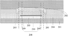
- FIG. 2A is a schematic top view of a thin film transistor 200 provided by a first embodiment of the present disclosure
- FIG. 2B is an example of a schematic sectional view of the thin film transistor of FIG. 2A along a section line C-C′
- FIG. 2C is another example of a schematic sectional view of the thin film transistor of FIG. 2A along the section line C-C′.
- the bottom-gate thin film transistor 200 comprises a gate electrode 202 , an auxiliary layer 203 , a gate insulating layer 204 , an active layer 205 , a source electrode 206 and a drain electrode 207 which are sequentially stacked on a substrate 201 .
- the active layer 205 comprises a channel region 208 between the source electrode 206 and the drain electrode 207 and the channel region 208 comprises an edge region 209 along a channel length direction and a main region 210 except the edge region 209 .
- a projection of the auxiliary layer 203 on the substrate 201 is at least partially overlapped with a projection of the edge region 209 of the channel region 208 on the substrate 201 , and the auxiliary layer 203 is configured to enhance a turn-on voltage of the edge region 209 of the channel region 208 .
- the auxiliary layer may be disposed between the gate electrode and the active layer.
- the auxiliary layer 203 is disposed corresponding to the edge region 209 of the channel region 208 , and projections of the gate electrode 202 , the auxiliary layer 203 and the active layer 205 on the substrate 201 are at least partially overlapped.
- the auxiliary layer 203 is disposed between the gate electrode 202 and the gate insulating layer 204 .
- a thickness of the auxiliary layer is less than one tenth of a thickness of the gate electrode.
- the thickness of the auxiliary layer is 15-30 nm, so as to prevent a step of the auxiliary layer in the bottom-gate structure from influencing a film formation quality of the active layer.
- the auxiliary layer 203 comprises two auxiliary gate electrodes which are spaced apart from each other, and the two auxiliary gate electrodes are disposed to respectively correspond to the two edge regions 209 of the channel region 208 .
- the auxiliary layer comprises only one auxiliary gate electrode which corresponds to only one edge region.
- the work function of the material of the gate electrode 202 is lower than the work function of the material of the auxiliary layer 203 .
- the material of the gate electrode 202 is molybdenum (Mo), of which the work function is 4.37 eV; the material of the auxiliary layer 203 is platinum (Pt), of which the work function is 5.65 eV.
- the difference between the work function of the material of the auxiliary layer 203 and the work function of the material of the active layer 205 is greater than a difference between the work function of the material of the gate electrode 202 and the work function of the material of the active layer 205 , so as to ultimately allow a turn-on voltage of the edge region 209 of the channel region 208 to be greater than a turn-on voltage of the main region 210 of the channel region 208 .
- auxiliary layer material is higher than the work function of the gate electrode material, so as to allow the difference between the work function of the auxiliary layer material and the work function of the active layer material to be greater than the difference between the work function of the gate electrode material and the work function of the active layer material.
- the material of the gate electrode is one or any combination of the following metal materials: copper (4.65 eV), molybdenum (4.37 eV), titanium (4.33 eV), tungsten (4.55 eV), and aluminum (4.28 eV); and the material of the auxiliary layer is one or any combination of the following metal materials: platinum (5.65 eV), gold (5.1 eV) and palladium (5.12 eV).
- the material of the gate electrode and the material of the auxiliary layer both may be a conductive material with an adjustable work function, for example, conductive silicon or a conductive metal oxide.
- the material of the gate electrode and the material of the auxiliary layer are both polysilicon, and a doping concentration of the polysilicon may be adjusted to allow the work function of the auxiliary gate electrode material to be higher than the work function of the gate electrode material.
- the material of the gate electrode and the material of the auxiliary gate electrode are both indium tin oxide (ITO), and a composition of the ITO may be adjusted to allow the work function of the auxiliary gate electrode material to be higher than the work function of the gate electrode material.
- FIG. 2C is another example of a schematic sectional view of the thin film transistor 200 of FIG. 2A along the section line C-C′.
- the auxiliary layer 203 and the gate electrode 202 are disposed in a same layer, that is, the auxiliary layer 203 and the gate electrode 202 are disposed on a same surface of the substrate 201 .
- the auxiliary layer 203 is disposed to correspond to the edge region 209 of the channel region 208 and the gate electrode 202 is disposed to correspond to the main region 210 of the channel region 208 .
- the auxiliary layer 203 may have a same thickness as the gate electrode 202 .
- FIG. 3 is a schematic sectional view of a thin film transistor 200 provided by a second embodiment of the present disclosure.
- the structure of the thin film transistor of the second embodiment is substantially same as the structure of the thin film transistor of the first embodiment, and the only differences are the location and the material of the auxiliary layer 203 .
- the auxiliary layer 203 is disposed between the active layer 205 and the gate insulating layer 204 .
- the auxiliary layer 203 is an auxiliary active layer and the material of the auxiliary layer 203 is a semiconductor material.
- the auxiliary layer 203 is two auxiliary active layers which are spaced from each other, and the two auxiliary active layers are disposed to respectively correspond to two edge regions 209 of the channel region 208 .
- the auxiliary layer comprises only one auxiliary active layer which corresponds to only one edge region of the channel region.
- the work function of the material of the active layer 205 is higher than the work function of the material of the auxiliary layer 203 .
- the material of the active layer and the auxiliary layer are both polysilicon. Polysilicons with different doping concentrations may be selected to allow the work function of the polysilicon material for the auxiliary layer 203 to be lower than work function of the polysilicon material for the active layer 205 .
- the difference between the work function of the material of the gate electrode 202 and the work function of the material of the auxiliary layer 203 is greater than the difference between the work function of the material of the gate electrode 202 and the work function of the material of the active layer 205 , so as to ultimately allow a turn-on voltage of the edge region 209 of the channel region 208 to be greater than a turn-on voltage of the main region 210 of the channel region.
- other combinations may be selected, in which the work function of the active layer material is higher than the work function of the auxiliary layer material, so as to allow the difference between the work function of the gate electrode material and the work function of the auxiliary layer layer material to be greater than the difference between the work function of the gate electrode material and the work function of the active layer material.
- FIG. 4A is a schematic top view of a thin film transistor 200 provided by a third embodiment of the present disclosure
- FIG. 4B is an example of a schematic sectional view of the thin film transistor 200 of FIG. 4A along a section line D-D′
- FIG. 4C is another example of a schematic sectional view of the thin film transistor 200 of FIG. 4A along the section line D-D′.
- same elements are indicated with same reference numbers, which is not repeated below.
- the top-gate thin film transistor 200 comprises a source electrode 206 and a drain electrode 207 , an active layer 205 , a gate insulating layer 204 , an auxiliary layer 203 and a gate electrode 202 which are sequentially stacked on a substrate 201 .
- the active layer 205 comprises a channel region 208 close to the gate insulating layer 204 and the channel region 208 comprises an edge region 209 along a channel length direction and a main region 210 other than the edge region 209 .
- a projection of the auxiliary layer 203 on the substrate 201 is at least partially overlapped with a projection of the edge region 209 of the channel region 208 on the substrate 201 , and the auxiliary layer 203 is configured to enhance a turn-on voltage of the edge region 209 of the channel region 208 .
- the auxiliary layer may be disposed between the gate electrode and the active layer.
- the auxiliary layer 203 is disposed corresponding to the edge region 209 of the channel region 208 , and projections of the gate electrode 202 , the auxiliary layer 203 and the active layer 205 on the substrate 201 are at least partially overlapped.
- the auxiliary layer 203 is disposed between the gate electrode 202 and the gate insulating layer 204 .
- the auxiliary layer 203 comprises two auxiliary gate electrodes which are spaced apart from each other, and the two auxiliary gate electrodes are disposed to respectively correspond to the two edge regions 209 of the channel region 208 .
- the auxiliary layer comprises only one auxiliary gate electrode which corresponds to only one edge region of the channel region.
- a work function of a material of the gate electrode 202 is lower than a work function of a material of the auxiliary layer 203 .
- the material of the gate electrode 202 is molybdenum (Mo), of which the work function is 4.37 eV; the material of the auxiliary layer 203 is platinum (Pt), of which the work function is 5.65 eV.
- the difference between the work function of the material of the auxiliary layer 203 and the work function of the material of the active layer 206 is greater than a difference between the work function of the material of the gate electrode 202 and the work function of the material of the active layer 205 , so as to ultimately allow a turn-on voltage of the edge region 209 of the channel region 208 to be greater than a turn-on voltage of the main region 210 of the channel region.
- auxiliary layer material is higher than the work function of the gate electrode material, so as to allow the difference between the work function of the auxiliary layer material and the work function of the active layer material to be greater than the difference between the work function of the gate electrode material and the work function of the active layer material.
- the material of the gate electrode is one or any combination of the following metal materials: copper (4.65 eV), molybdenum (4.37 eV), titanium (4.33 eV), tungsten (4.55 eV), and aluminum (4.28 eV); and the material of the auxiliary layer is one or any combination of the following metal materials: platinum (5.65 eV), gold (5.1 eV) and palladium (5.12 eV).
- the material of the gate electrode and the material of the auxiliary layer both may be a conductive material with an adjustable work function, for example, conductive silicon or a conductive metal oxide.
- the material of the gate electrode and the material of the auxiliary layer both are polysilicon, and a doping concentration of the polysilicon may be adjusted to allow the work function of the auxiliary gate electrode material to be higher than the work function of the gate electrode material.
- the material of the gate electrode and the material of the auxiliary gate electrode are both indium tin oxide (ITO), and a composition of the ITO may be adjusted to allow the work function of the auxiliary gate electrode material to be higher than the work function of the gate electrode material.
- FIG. 4C is another example of a schematic sectional view of the thin film transistor 200 of FIG. 4A along the section line C-C′.
- the auxiliary layer 203 and the gate electrode 202 are disposed in a same layer, that is, the auxiliary layer 203 and the gate electrode 202 are disposed on a same surface of the gate insulating layer 204 .
- the auxiliary layer 203 is disposed to correspond to the edge region 209 of the channel region 208 and the gate electrode 202 is disposed to correspond to the main region 210 of the channel region 208 .
- the auxiliary layer 203 may have a same thickness as the gate electrode 202 .
- FIG. 5 is a schematic sectional view of a thin film transistor 200 provided by a fourth embodiment of the present disclosure.
- the structure of the thin film transistor of the fourth embodiment is almost same as the structure of the thin film transistor of the third embodiment, and the only differences are the location and the material of the auxiliary layer 203 .
- the auxiliary layer 203 is disposed between the active layer 205 and the gate insulating layer 204 .
- the auxiliary layer 203 is an auxiliary active layer and a material of the auxiliary layer 203 is a semiconductor material.
- the auxiliary layer comprises two auxiliary active layers which are spaced from each other, and the two auxiliary active layers are disposed respectively on two edge regions 209 of the channel region 208 .
- the auxiliary comprises only one auxiliary active layer which corresponds to only one edge region of the channel region.
- the work function of the material of the active layer 205 is higher than the work function of the material of the auxiliary layer 203 .
- the material of the active layer and the auxiliary layer are both polysilicon. Polysilicons with different doping concentrations may be selected to allow the work function of the polysilicon material for the auxiliary layer 203 to be lower than work function of the polysilicon material for the active layer 205 .
- the difference between the work function of the material of the gate electrode 202 and the work function of the material of the auxiliary layer 203 is greater than the difference between the work function of the material of the gate electrode 202 and the work function of the material of the active layer 205 , so as to ultimately allow a turn-on voltage of the edge region 209 of the channel region 208 to be greater than a turn-on voltage of the main region 210 of the channel region.
- other combinations may be selected, in which the work function of the active layer material is higher than the work function of the auxiliary layer material, so as to allow the difference between the work function of the gate electrode material and the work function of the auxiliary layer material to be greater than the difference between the work function of the gate electrode material and the work function of the active layer material.
- the thin film transistor according to this embodiment enhances the turn-on voltage of the edge region of the channel region by providing the auxiliary layer between the gate electrode and the active layer corresponding to the edge region along the channel length direction of the channel region, so as to allow a turn-on current to be almost synchronously generated in the edge region as well as in the main region of the channel region. In this way, the hump effect of the thin film transistor is alleviated or eliminated and the performance of the thin film transistor is improved.
- embodiments of the present disclosure further provide a manufacturing method of a thin film transistor which may be used for manufacturing the thin film transistors of the above mentioned embodiments.
- the method at least comprises: forming a gate electrode, an auxiliary layer, a gate insulating layer, an active layer, a source electrode and a drain electrode on a substrate; forming the auxiliary layer between a step of forming the gate electrode and a step of forming the active layer.
- the active layer comprises a channel region between the source electrode and the drain electrode and the channel region comprises an edge region along a channel length direction and a main region outside the edge region.
- a projection of the auxiliary layer on the substrate is at least partially overlapped with a projection of the edge region of the channel region on the substrate, and the auxiliary layer is configured to enhance a turn-on voltage of the edge region of the channel region.
- the gate electrode and the auxiliary layer may be respectively formed through an exposure process, or formed through one exposure process with a gray tone mask.
- the active layer and the auxiliary layer may be respectively formed through an exposure process, or formed through one exposure process with a gray tone mask.
- the auxiliary layer is formed between the gate electrode and the active layer.
- FIGS. 6A-6C and FIG. 7 The manufacturing method of a thin film transistor provided by a fifth embodiment and a modified embodiment thereof of the present disclosure is described in combination with FIGS. 6A-6C and FIG. 7 .
- Step S 61 forming a gate electrode 202 .
- a first conductive layer is formed on a substrate 201 and a gate electrode 202 is formed by patterning the first conductive layer using a first patterning process.
- the substrate 201 is provided and then the substrate is cleaned and dried.
- the substrate 201 may be a bendable flexible substrate, for example, a substrate made of various kinds of plastic films such as polyethylene terephthalate (PET), polyether sulfone (PES), polycarbonate (PC) polyimide (PI) or derivative of the above.
- the substrate 201 may be a rigid substrate, such as a glass substrate, a stainless steel substrate and the like.
- Step S 62 forming an auxiliary layer 203 , and the auxiliary gate electrode 203 and the gate electrode 202 are formed to be electrically connected with each other.
- a second conductive layer is formed on the gate electrode 202 and is patterned to form an auxiliary layer 203 .
- the auxiliary layer 203 is formed on an edge region of the gate electrode 202 along a channel length direction of the thin film transistor to be formed.
- the auxiliary layer 203 is formed to be two auxiliary gate electrodes which are spaced apart from each other and respectively correspond to two edge regions 209 of a channel region 208 .
- the auxiliary layer comprises only one auxiliary gate electrode which corresponds to only one edge region of the channel region, and a thickness of the auxiliary layer is less than one tenth of a thickness of the gate electrode.
- the thickness of the auxiliary layer is 15-30 nm, so as to prevent a step of the auxiliary layer in the bottom-gate structure from influencing a film formation quality of an active layer.
- a work function of a material of the first conductive layer is selected to be lower than a work function of a material of the second conductive layer, so as to allow a work function of a material of the gate electrode 202 to be lower than a work function of a material of the auxiliary layer 203 .
- the material of the first conductive layer is molybdenum (Mo), of which the work function is 4.37 eV; the material of the second conductive layer is platinum (Pt), of which the work function is 5.65 eV.
- Mo molybdenum
- the material of the second conductive layer is platinum (Pt), of which the work function is 5.65 eV.
- the material of the first conductive layer is one or any combination of the following metal materials: copper (4.65 eV), molybdenum (4.37 eV), titanium (4.33 eV), tungsten (4.55 eV), and aluminum (4.28 eV); and the material of the second conductive layer is one or any combination of the following metal materials: platinum (5.65 eV), gold (5.1 eV) and palladium (5.12 eV).
- the material of the first conductive layer and the material of the second conductive layer both may be a conductive material with an adjustable work function, for example, conductive silicon or a conductive metal oxide.
- the material of the first conductive layer and the material of the second conductive layer both are polysilicon, and a doping concentration of the polysilicon may be adjusted to allow the work function of the second conductive layer material to be higher than the work function of the first conductive layer material.
- the material of the first conductive layer and the material of the second conductive layer are both indium tin oxide (ITO), and a composition of the ITO may be adjusted to allow the work function of the second conductive layer material to be higher than the work function of the first conductive layer material.
- the gate electrode 202 and the auxiliary layer 203 may be formed through one exposure process.
- the gate electrode 202 and the auxiliary layer 203 may be formed through one exposure process with a half tone mask.
- FIG. 6B in combination with FIG. 6C , after the first conductive layer 301 and the second conductive layer 302 are sequentially formed on the substrate 201 , a photoresist layer 310 is formed on the second conductive layer 302 and an exposure process is performed to the photoresist layer 310 with a half tone mask 320 .
- the half tone mask 320 comprises three regions A, B and C which are symmetrically distributed and have different light transmittance.
- the region A is a completely-transparent region
- the region B is a non-transparent region
- the region C is a partially-transparent region.
- the gate electrode 202 and the auxiliary layer 203 may be formed in a same layer; that is, the gate electrode 202 and the auxiliary layer 203 may be formed on a same surface of the substrate 201 .
- the gate electrode 202 and the auxiliary layer 203 may be respectively formed through performing a deposition process and a patterning process of a conductive material twice, which is not repeated here.
- a thickness of the auxiliary layer 203 is same as a thickness of the gate electrode 202 .
- Step S 63 forming a gate insulating layer and an active layer 205 .
- a gate insulating layer 204 is formed on the auxiliary layer 203 , and subsequently a semiconductor layer is formed on the gate insulating layer 204 . Then an active layer 205 is formed by patterning the conductive layer using a third patterning process.
- the active layer 205 comprises a channel region 208 close to the gate insulating layer 204 and the channel region 208 comprises two edge regions 209 and a main region 210 other than the edge regions 209 , and the two edge regions 209 are opposite to each other along a channel length direction.
- the two edge regions 209 correspond to the auxiliary layer 203 ; that is, the two edge regions 209 respectively correspond to two auxiliary gate electrodes, and a projection of each of the two edge regions 209 on the substrate 201 is at least partially overlapped with a projection of the corresponding auxiliary gate electrode on the substrate 201 .
- projections of the gate electrode 202 , the auxiliary layer 203 and the active layer 205 on the substrate 201 are at least partially overlapped.
- Step S 64 forming a source electrode and a drain electrode (not shown).
- a third conductive layer is formed on the active layer 205 and a source electrode 206 and a drain electrode 207 are formed by using a fourth patterning process to pattern the third conductive layer.
- the third conductive layer may be selected from materials molybdenum, titanium, aluminum, copper and alloy of the above.
- the thin film transistor 200 of the first embodiment of the present disclosure is formed.
- the step for forming the auxiliary layer 203 is after forming the gate insulating layer 204 and before forming the active layer 205 .
- a material of the auxiliary layer 203 is a semiconductor material and the auxiliary layer 203 functions as an auxiliary active layer.
- a number of the auxiliary active layer is two, and the two auxiliary active layers are disposed to respectively correspond to the two edge regions 209 of the channel region 208 .
- a work function of a material of the auxiliary layer 203 is enabled to lower than a work function of a material of the active layer 205 , so that a turn-on voltage of the edge region 209 is enhanced. In this way, the thin film transistor 200 of the second embodiment of the present disclosure is formed.
- the materials of the active layer and the auxiliary layer are both polysilicon.
- Polysilicons with different doping concentrations may be selected to allow the work function of the polysilicon material for the auxiliary layer to be lower than the work function of the polysilicon material for the active layer.
- the difference between the work function of the gate electrode material and the work function of the auxiliary layer material is greater than the difference between the work function of the gate electrode material and the work function of the active layer material, so as to ultimately allow a turn-on voltage of the edge region 209 of the channel region 208 to be greater than a turn-on voltage of the main region 210 of the channel region.
- components such as a storage capacitor and a pixel electrode may be formed meanwhile forming the thin film transistor.
- Step S 81 forming an active layer 205 .
- the substrate 201 is provided and then the substrate 201 is cleaned and dried.
- the substrate 201 may be a bendable flexible substrate, for example, a substrate made of various kinds of plastic films such as polyethylene terephthalate (PET), polyether sulfone (PES), polycarbonate (PC) polyimide (PI) or derivative of the above.
- the substrate 201 may be a rigid substrate, such as a glass substrate, a stainless steel substrate and the like.
- a first semiconductor layer is formed on the substrate 201 and an active layer 205 is formed by using a first patterning process to pattern the first semiconductor layer.
- the active layer 205 comprises a channel region 208 away from the substrate 201 .
- the channel region 208 comprises two edge regions 209 and a main region 210 except the two edge regions 209 .
- the two edge regions 209 are opposite to each other along a channel length direction.
- a buffer layer may be further formed between the substrate 201 and the active layer 205 .
- the buffer layer can prevent impurities of the substrate from diffusing into the active layer and affecting a performance of the active layer.
- Step S 82 forming an auxiliary layer 203 .
- a second semiconductor layer is formed on the active layer 205 and an auxiliary layer 203 is formed by performing a patterning process to the second semiconductor layer.
- the auxiliary layer 203 is formed on the edge region 209 of the active layer 205 .
- a work function of a material of the first semiconductor layer is enabled to have a special relationship with a work function of a material of the second semiconductor layer so as to enhance a turn-on voltage of the edge region 209 of the channel region.
- the auxiliary layer 203 comprises two auxiliary active layers which are spaced apart from each other and are respectively formed on the two edge regions 209 of the active layer 205 .
- the auxiliary layer comprises only one auxiliary active layer which corresponds to only one edge region of the channel region.
- the material of the first semiconductor layer and the material of the semiconductor layer both are polysilicon, and a doping concentration of the polysilicon may be adjusted to allow the work function of the polysilicon material of the second semiconductor layer material to be lower than the work function of the polysilicon material of the first semiconductor layer material, so as to allow a work function of the auxiliary layer material to be lower than a work function of the active layer material.
- the active layer 205 and the auxiliary layer 203 may be formed through one exposure process.
- the active layer 205 and the auxiliary layer 203 are formed through one exposure process with a half tone mask.
- the specific method is similar to the step for forming the gate electrode 202 and the auxiliary layer 203 through one exposure process in the fifth embodiment, which is not repeated here.
- Step S 83 forming a gate insulating layer, a gate electrode, a source electrode and a drain electrode.
- a gate insulating layer 204 is formed on the auxiliary layer 203 and then a conductive layer is formed on the gate insulating layer 204 .
- a gate electrode 202 , a source electrode and a drain electrode (not shown) are formed by using a third patterning process to pattern the conductive layer. In this way, the thin film transistor 200 of the fourth embodiment of the present disclosure is formed.
- projections of the gate electrode 202 , the auxiliary layer 203 and the active layer 205 on the substrate 201 are at least partially overlapped.
- a work function of the first semiconductor layer material is selected to be higher than a work function of the second semiconductor layer material to allow the work function of the auxiliary layer layer material to be lower than the work function of the active layer material.
- a work function difference between the gate electrode material and the auxiliary layer material is greater than a work function difference between the gate electrode material and the active layer material so as to ultimately allow a turn-on voltage of the edge region 209 of the channel region 208 to be higher than a turn-on voltage of the main region 210 .
- the step for forming the auxiliary layer 203 happens before forming the gate insulating layer 204 and before or after forming the gate electrode 202 .
- a material of the auxiliary layer 203 is a conductive material
- the auxiliary layer 203 is as the auxiliary gate electrode.
- a work function of a material of the auxiliary layer 203 is enabled to be higher than a work function of a material of the gate electrode 202 , so that a turn-on voltage of the edge region 209 is enhanced.
- the auxiliary layer 203 is formed between the gate electrode 202 and the gate insulating layer 204 , so that the thin film transistor 200 as illustrated in FIG. 4B is formed.
- the auxiliary layer 203 is formed in a same layer with the gate electrode 202 ; that is, the auxiliary layer 203 and the gate electrode 202 are formed on a same surface of the gate insulating layer 204 .
- the thin film transistor 200 as illustrated in FIG. 4C is formed.
- the gate electrode 202 and the auxiliary layer 203 may be respectively formed through performing a deposition process and a patterning process to a conductive material twice, which is not repeated here.
- a thickness of the auxiliary layer 203 is identical with a thickness of the gate electrode 202 .
- the material of the gate electrode is molybdenum (Mo), of which the work function is 4.37 eV; the material of the auxiliary layer is platinum (Pt), of which the work function is 5.65 eV.
- Mo molybdenum
- Pt platinum
- the difference between the work function of the material of the auxiliary layer 203 and the work function of the material of the active layer is greater than a difference between the work function of the material of the gate electrode 202 and the work function of the material of the active layer.
- the material of the gate electrode is one or any combination of the following metal materials: copper (4.65 eV), molybdenum (4.37 eV), titanium (4.33 eV), tungsten (4.55 eV), and aluminum (4.28 eV); and the material of the auxiliary layer is one or any combination of the following metal materials: platinum (5.65 eV), gold (5.1 eV) and palladium (5.12 eV).
- the material of the gate electrode and the material of the auxiliary layer both may be a conductive material with an adjustable work function, for example, conductive silicon or a conductive metal oxide.
- the material of the gate electrode and the material of the auxiliary layer are both polysilicon, and a doping concentration of the polysilicon may be adjusted to allow the work function of the auxiliary layer material to be higher than the work function of the gate electrode material.
- the material of the gate electrode and the material of the auxiliary layer are both indium tin oxide (ITO), and a composition of the ITO may be adjusted to allow the work function of the auxiliary layer material to be higher than the work function of the gate electrode material.
- components such as a storage capacitor and a pixel electrode may be formed meanwhile forming the thin film transistor.
- a work function difference of metal-semiconductor corresponding to the edge region of the channel region of the active layer is allowed to be higher than a work function difference of metal-semiconductor corresponding to the main region of the channel region, so that the turn-on voltage of the edge region of the channel region is enhanced and a turn-on current is almost synchronously generated in the edge region as well as in the main region of the channel region.
- the hump effect of the thin film transistor is alleviated or eliminated and the performance of the thin film transistor is improved.
- An embodiment of the present disclosure further provides an electronic device, and the electronic device comprises the thin film transistor 200 according to any one embodiment of the present disclosure.
- the electronic device is a display device such as a liquid crystal display device, an organic light-emitting diode display device and an e-paper display device.
- a pixel unit of the display device comprises the thin film transistor 200 .
- a driving circuit of the display device comprises the thin film transistor 200 .
- the display decide may comprise an array substrate, the thin film transistor of the above mentioned pixel unit or driving circuit (i. e. GOA) is formed on the array substrate and the thin film transistor may adopt the thin film transistor of any one embodiment of the present disclosure.
- GOA driving circuit
- FIG. 11 is a schematic diagram of an electronic device 400 provided by a seventh embodiment of the present disclosure and FIG. 12 is schematic view of a pixel circuit of the electronic device of FIG. 11 .
- the electronic device 400 is an organic light-emitting diode display device.
- the organic light-emitting diode display device comprises a plurality of pixel units 401 arranged in an array, each pixel unit 401 comprises at least one organic light-emitting diode and a pixel circuit connected with the organic light-emitting diode, and the organic light-emitting diode is driven to emit light by the pixel circuit.
- FIG. 12 is a schematic view of a 2T1C pixel circuit of an organic light-emitting diode electronic device.
- the pixel circuit comprises a switch transistor T 1 , a driving transistor T 2 and a storage capacitor Cs.
- a gate electrode of the switch transistor T 1 is connected with a gate line to receive a scan signal (Scan), a source electrode is connected with a data line to receive a data signal (Vdata) for example, and a drain electrode is connected with a gate electrode of the driving transistor T 2 .
- a source electrode of the driving transistor T 2 is connected with a first power source terminal (Vdd, a high voltage terminal) and a drain electrode is connected with a positive end of OLED.
- a driving manner of the 2T1C pixel circuit is to control bright and dark (a greyscale) of a pixel by two TFTs and a storage capacitor Cs.
- the data voltage (Vdata) which is sent through the data line by a data driving circuit sends charges the storage capacitor Cs through the switch transistor T 1 , so as to store the data voltage in the storage capacitor Cs.
- the stored data voltage controls a conduction degree of the driving transistor T 2 so as to control a current value of current which runs through the driving transistor to drive the OLED to emit light; that is, the current determines an emission greyscale of the OLED.
- the switch transistor T 1 and the driving transistor T 2 both may adopt the thin film transistor 200 of the embodiments of the present disclosure for example.
- the organic light-emitting diode display device may further comprise a data driving circuit 6 and a gate driving circuit 7 .
- the data driving circuit 6 is configured to provide a data signal and the gate driving circuit 7 is configured to provide a scan signal (e. g. the signal Vscan) and may be further configured to provide various kinds of control signals.
- the data driving circuit 6 is electrically connected with the pixel unit 401 through the data line 61
- the gate driving circuit 7 is electrically connected with the pixel unit 401 through the gate line 71 .
- the data driving circuit 6 and the gate driving circuit 7 both comprises a thin film transistor which may adopt the thin film transistor 200 of the embodiments of the present disclosure for example.
- the display device may be applied in any product or component having display functions such as a cellphone, a tablet computer, a television, a displayer, a notebook computer, a digital photo frame, a navigator and the like.
Landscapes
- Engineering & Computer Science (AREA)
- Power Engineering (AREA)
- Microelectronics & Electronic Packaging (AREA)
- Physics & Mathematics (AREA)
- Condensed Matter Physics & Semiconductors (AREA)
- General Physics & Mathematics (AREA)
- Computer Hardware Design (AREA)
- Ceramic Engineering (AREA)
- Manufacturing & Machinery (AREA)
- Chemical & Material Sciences (AREA)
- Crystallography & Structural Chemistry (AREA)
- Thin Film Transistor (AREA)
Applications Claiming Priority (3)
| Application Number | Priority Date | Filing Date | Title |
|---|---|---|---|
| CN201710835326.XA CN109509793B (zh) | 2017-09-15 | 2017-09-15 | 薄膜晶体管、其制造方法及电子装置 |
| CN201710835326.X | 2017-09-15 | ||
| PCT/CN2018/094117 WO2019052265A1 (zh) | 2017-09-15 | 2018-07-02 | 薄膜晶体管、其制造方法及电子装置 |
Related Parent Applications (1)
| Application Number | Title | Priority Date | Filing Date |
|---|---|---|---|
| PCT/CN2018/094117 A-371-Of-International WO2019052265A1 (zh) | 2017-09-15 | 2018-07-02 | 薄膜晶体管、其制造方法及电子装置 |
Related Child Applications (1)
| Application Number | Title | Priority Date | Filing Date |
|---|---|---|---|
| US17/806,578 Continuation US11837665B2 (en) | 2017-09-15 | 2022-06-13 | Thin film transistor and manufacturing method thereof and electronic device |
Publications (2)
| Publication Number | Publication Date |
|---|---|
| US20210343875A1 US20210343875A1 (en) | 2021-11-04 |
| US11387371B2 true US11387371B2 (en) | 2022-07-12 |
Family
ID=65722410
Family Applications (2)
| Application Number | Title | Priority Date | Filing Date |
|---|---|---|---|
| US16/330,255 Active 2040-05-24 US11387371B2 (en) | 2017-09-15 | 2018-07-02 | Thin film transistor and manufacturing method thereof and electronic device |
| US17/806,578 Active US11837665B2 (en) | 2017-09-15 | 2022-06-13 | Thin film transistor and manufacturing method thereof and electronic device |
Family Applications After (1)
| Application Number | Title | Priority Date | Filing Date |
|---|---|---|---|
| US17/806,578 Active US11837665B2 (en) | 2017-09-15 | 2022-06-13 | Thin film transistor and manufacturing method thereof and electronic device |
Country Status (4)
| Country | Link |
|---|---|
| US (2) | US11387371B2 (zh) |
| EP (1) | EP3683846A4 (zh) |
| CN (1) | CN109509793B (zh) |
| WO (1) | WO2019052265A1 (zh) |
Families Citing this family (4)
| Publication number | Priority date | Publication date | Assignee | Title |
|---|---|---|---|---|
| US11239313B2 (en) * | 2018-10-30 | 2022-02-01 | Taiwan Semiconductor Manufacturing Company, Ltd. | Integrated chip and method of forming thereof |
| CN110060998B (zh) * | 2019-04-29 | 2022-05-17 | 厦门天马微电子有限公司 | 一种反相电路结构、栅极驱动电路及显示面板 |
| CN111048524A (zh) * | 2019-11-26 | 2020-04-21 | 深圳市华星光电半导体显示技术有限公司 | 阵列基板及制备方法、显示面板 |
| CN114823730A (zh) * | 2022-04-20 | 2022-07-29 | 广州华星光电半导体显示技术有限公司 | 显示面板和显示装置 |
Citations (6)
| Publication number | Priority date | Publication date | Assignee | Title |
|---|---|---|---|---|
| US20080012023A1 (en) | 2006-07-12 | 2008-01-17 | Mieko Matsumura | Thin-film transistor and image display device |
| US8217456B1 (en) | 2011-03-11 | 2012-07-10 | International Business Machines Corporation | Low capacitance hi-K dual work function metal gate body-contacted field effect transistor |
| US20170074619A1 (en) * | 2015-09-10 | 2017-03-16 | The Boeing Company | Methods of connecting testing equipment to a missile system |
| KR20170074619A (ko) * | 2015-12-22 | 2017-06-30 | 엘지이노텍 주식회사 | 박막 트랜지스터 기판, 이를 포함하는 표시패널 및 표시장치 |
| US20180033804A1 (en) * | 2016-07-29 | 2018-02-01 | Lg Display Co., Ltd. | Thin Film Transistor, Method for Manufacturing the Same, and Display Device Including the Same |
| US20190074377A1 (en) * | 2017-09-01 | 2019-03-07 | Samsung Display Co., Ltd. | Thin film transistor and display device including the same |
Family Cites Families (17)
| Publication number | Priority date | Publication date | Assignee | Title |
|---|---|---|---|---|
| JP3036513B2 (ja) * | 1998-06-10 | 2000-04-24 | 日本電気株式会社 | 液晶表示装置 |
| CN1217417C (zh) * | 1999-12-10 | 2005-08-31 | 株式会社半导体能源研究所 | 半导体器件及其制造方法 |
| US7256079B2 (en) * | 2002-12-16 | 2007-08-14 | Semiconductor Energy Laboratory Co., Ltd. | Evaluation method using a TEG, a method of manufacturing a semiconductor device having a TEG, an element substrate and a panel having the TEG, a program for controlling dosage and a computer-readable recording medium recoding the program |
| US7282782B2 (en) * | 2004-03-12 | 2007-10-16 | Hewlett-Packard Development Company, L.P. | Combined binary oxide semiconductor device |
| CN100533236C (zh) * | 2005-11-29 | 2009-08-26 | 中华映管股份有限公司 | 像素结构 |
| JP4934599B2 (ja) * | 2007-01-29 | 2012-05-16 | キヤノン株式会社 | アクティブマトリクス表示装置 |
| US7947582B2 (en) * | 2009-02-27 | 2011-05-24 | Tel Epion Inc. | Material infusion in a trap layer structure using gas cluster ion beam processing |
| US9312260B2 (en) * | 2010-05-26 | 2016-04-12 | Taiwan Semiconductor Manufacturing Company, Ltd. | Integrated circuits and manufacturing methods thereof |
| KR101973212B1 (ko) * | 2010-11-05 | 2019-04-26 | 가부시키가이샤 한도오따이 에네루기 켄큐쇼 | 반도체 장치 |
| US9525071B2 (en) * | 2012-02-22 | 2016-12-20 | Massachusetts Institute Of Technology | Flexible high-voltage thin film transistors |
| GB201304613D0 (en) * | 2013-03-14 | 2013-05-01 | Cambridge Display Tech Ltd | Blend |
| EP2960943B1 (en) * | 2014-06-27 | 2019-08-07 | LG Display Co., Ltd. | Thin film transistor of display apparatus |
| TW201614850A (en) * | 2014-10-01 | 2016-04-16 | Chunghwa Picture Tubes Ltd | Thin film transistor and manufacturing method thereof |
| CN105097898B (zh) * | 2015-06-02 | 2019-12-31 | 京东方科技集团股份有限公司 | 一种薄膜晶体管、阵列基板及显示装置 |
| CN108140581B (zh) * | 2015-09-30 | 2021-09-07 | 国立研究开发法人科学技术振兴机构 | 隧道场效应晶体管 |
| CN106847931A (zh) * | 2017-04-05 | 2017-06-13 | 厦门天马微电子有限公司 | 一种薄膜晶体管、阵列基板及显示装置 |
| US11404536B2 (en) * | 2018-03-30 | 2022-08-02 | Intel Corporation | Thin-film transistor structures with gas spacer |
-
2017
- 2017-09-15 CN CN201710835326.XA patent/CN109509793B/zh active Active
-
2018
- 2018-07-02 EP EP18849422.3A patent/EP3683846A4/en active Pending
- 2018-07-02 WO PCT/CN2018/094117 patent/WO2019052265A1/zh unknown
- 2018-07-02 US US16/330,255 patent/US11387371B2/en active Active
-
2022
- 2022-06-13 US US17/806,578 patent/US11837665B2/en active Active
Patent Citations (6)
| Publication number | Priority date | Publication date | Assignee | Title |
|---|---|---|---|---|
| US20080012023A1 (en) | 2006-07-12 | 2008-01-17 | Mieko Matsumura | Thin-film transistor and image display device |
| US8217456B1 (en) | 2011-03-11 | 2012-07-10 | International Business Machines Corporation | Low capacitance hi-K dual work function metal gate body-contacted field effect transistor |
| US20170074619A1 (en) * | 2015-09-10 | 2017-03-16 | The Boeing Company | Methods of connecting testing equipment to a missile system |
| KR20170074619A (ko) * | 2015-12-22 | 2017-06-30 | 엘지이노텍 주식회사 | 박막 트랜지스터 기판, 이를 포함하는 표시패널 및 표시장치 |
| US20180033804A1 (en) * | 2016-07-29 | 2018-02-01 | Lg Display Co., Ltd. | Thin Film Transistor, Method for Manufacturing the Same, and Display Device Including the Same |
| US20190074377A1 (en) * | 2017-09-01 | 2019-03-07 | Samsung Display Co., Ltd. | Thin film transistor and display device including the same |
Non-Patent Citations (2)
| Title |
|---|
| Ali A. Orouji, et al; "Leakage Current Reduction Techniques in Poly-Si TFTs for Active Matrix Liquid Crystal Displays: A Comprehensive Study", IEEE Transactions on Device and Materials Reliability, vol. 6, No. 2, Jun. 2006, pp. 315-325. |
| The Extended European Search Report dated Jul. 30, 2021; Appln. No. 18849422.3. |
Also Published As
| Publication number | Publication date |
|---|---|
| CN109509793A (zh) | 2019-03-22 |
| US11837665B2 (en) | 2023-12-05 |
| EP3683846A1 (en) | 2020-07-22 |
| EP3683846A4 (en) | 2021-09-01 |
| CN109509793B (zh) | 2020-12-01 |
| US20210343875A1 (en) | 2021-11-04 |
| US20220310850A1 (en) | 2022-09-29 |
| WO2019052265A1 (zh) | 2019-03-21 |
Similar Documents
| Publication | Publication Date | Title |
|---|---|---|
| US11837665B2 (en) | Thin film transistor and manufacturing method thereof and electronic device | |
| CN107731858B (zh) | 一种阵列基板、其制作方法及显示面板 | |
| US10367073B2 (en) | Thin film transistor (TFT) with structured gate insulator | |
| US10558097B2 (en) | Active matrix substrate and demultiplexer circuit | |
| US11088230B2 (en) | Pixel circuit, manufacturing method thereof, and display device | |
| US10886409B2 (en) | Display backplate and fabrication method thereof, display panel and display device | |
| US20180012950A1 (en) | Organic light emitting diode display | |
| CN106920804B (zh) | 一种阵列基板、其驱动方法、显示面板及显示装置 | |
| WO2021254053A1 (zh) | 显示基板及其制备方法、驱动方法、显示装置 | |
| US9947691B2 (en) | Array substrate, manufacturing method thereof and display panel | |
| US11133366B2 (en) | Array substrate and method of manufacturing the same, and display device | |
| US20190229169A1 (en) | Display panel and manufacturing method therefor, and display apparatus | |
| US11362118B2 (en) | Array substrate, manufacturing method thereof, and display panel | |
| US11355647B2 (en) | Thin film transistor and manufacturing method thereof and electronic device | |
| KR102308621B1 (ko) | 박막 트랜지스터 표시판 및 그 제조 방법 | |
| US11158628B2 (en) | Electro-static discharge circuit, array substrate, display panel and display apparatus | |
| US9905588B2 (en) | Organic light emitting display panel and method of manufacturing the same | |
| CN113192986B (zh) | 显示面板及其制备方法 | |
| CN113903751A (zh) | 薄膜晶体管阵列衬底和显示器件 | |
| US11482546B2 (en) | Method of fabricating array substrate | |
| US11455955B2 (en) | Display device | |
| US20230086999A1 (en) | Gate driving circuit and manufacturing method therefor, array substrate, and display device | |
| US20060267050A1 (en) | Method for driving active display | |
| US20230420462A1 (en) | Array substrate, preparation method thereof, display panel and display device | |
| CN105789319A (zh) | 薄膜晶体管及其制备方法 |
Legal Events
| Date | Code | Title | Description |
|---|---|---|---|
| AS | Assignment |
Owner name: BOE TECHNOLOGY GROUP CO., LTD., CHINA Free format text: ASSIGNMENT OF ASSIGNORS INTEREST;ASSIGNOR:RIM, SEUNG MOO;REEL/FRAME:048494/0881 Effective date: 20190212 Owner name: CHONGQING BOE OPTOELECTRONICS TECHNOLOGY CO., LTD., CHINA Free format text: ASSIGNMENT OF ASSIGNORS INTEREST;ASSIGNOR:RIM, SEUNG MOO;REEL/FRAME:048494/0881 Effective date: 20190212 Owner name: BOE TECHNOLOGY GROUP CO., LTD., CHINA Free format text: ASSIGNMENT OF ASSIGNORS INTEREST;ASSIGNOR:ZHAO, YONGLIANG;REEL/FRAME:048494/0794 Effective date: 20190212 Owner name: CHONGQING BOE OPTOELECTRONICS TECHNOLOGY CO., LTD., CHINA Free format text: ASSIGNMENT OF ASSIGNORS INTEREST;ASSIGNOR:ZHAO, YONGLIANG;REEL/FRAME:048494/0794 Effective date: 20190212 Owner name: BOE TECHNOLOGY GROUP CO., LTD., CHINA Free format text: ASSIGNMENT OF ASSIGNORS INTEREST;ASSIGNOR:HUANG, ZHONGHAO;REEL/FRAME:048494/0704 Effective date: 20190212 Owner name: CHONGQING BOE OPTOELECTRONICS TECHNOLOGY CO., LTD., CHINA Free format text: ASSIGNMENT OF ASSIGNORS INTEREST;ASSIGNOR:HUANG, ZHONGHAO;REEL/FRAME:048494/0704 Effective date: 20190212 Owner name: BOE TECHNOLOGY GROUP CO., LTD., CHINA Free format text: ASSIGNMENT OF ASSIGNORS INTEREST;ASSIGNOR:WANG, JUN;REEL/FRAME:048494/0556 Effective date: 20190212 Owner name: CHONGQING BOE OPTOELECTRONICS TECHNOLOGY CO., LTD., CHINA Free format text: ASSIGNMENT OF ASSIGNORS INTEREST;ASSIGNOR:WANG, JUN;REEL/FRAME:048494/0556 Effective date: 20190212 |
|
| FEPP | Fee payment procedure |
Free format text: ENTITY STATUS SET TO UNDISCOUNTED (ORIGINAL EVENT CODE: BIG.); ENTITY STATUS OF PATENT OWNER: LARGE ENTITY |
|
| STPP | Information on status: patent application and granting procedure in general |
Free format text: DOCKETED NEW CASE - READY FOR EXAMINATION |
|
| STPP | Information on status: patent application and granting procedure in general |
Free format text: NON FINAL ACTION MAILED |
|
| STPP | Information on status: patent application and granting procedure in general |
Free format text: RESPONSE TO NON-FINAL OFFICE ACTION ENTERED AND FORWARDED TO EXAMINER |
|
| STPP | Information on status: patent application and granting procedure in general |
Free format text: NOTICE OF ALLOWANCE MAILED -- APPLICATION RECEIVED IN OFFICE OF PUBLICATIONS |
|
| STCF | Information on status: patent grant |
Free format text: PATENTED CASE |