US11217748B2 - Semiconductor device including a data storage material pattern - Google Patents
Semiconductor device including a data storage material pattern Download PDFInfo
- Publication number
- US11217748B2 US11217748B2 US16/807,245 US202016807245A US11217748B2 US 11217748 B2 US11217748 B2 US 11217748B2 US 202016807245 A US202016807245 A US 202016807245A US 11217748 B2 US11217748 B2 US 11217748B2
- Authority
- US
- United States
- Prior art keywords
- pattern
- data storage
- conductive
- spacer
- storage material
- Prior art date
- Legal status (The legal status is an assumption and is not a legal conclusion. Google has not performed a legal analysis and makes no representation as to the accuracy of the status listed.)
- Active, expires
Links
- 238000013500 data storage Methods 0.000 title claims abstract description 191
- 239000011232 storage material Substances 0.000 title claims abstract description 170
- 239000004065 semiconductor Substances 0.000 title claims abstract description 68
- 239000000463 material Substances 0.000 claims abstract description 62
- 239000000758 substrate Substances 0.000 claims abstract description 20
- 125000006850 spacer group Chemical group 0.000 claims description 252
- 230000001681 protective effect Effects 0.000 claims description 77
- 238000000034 method Methods 0.000 description 48
- 238000005530 etching Methods 0.000 description 26
- 238000010586 diagram Methods 0.000 description 24
- 238000004140 cleaning Methods 0.000 description 15
- VYPSYNLAJGMNEJ-UHFFFAOYSA-N Silicium dioxide Chemical compound O=[Si]=O VYPSYNLAJGMNEJ-UHFFFAOYSA-N 0.000 description 14
- 239000000956 alloy Substances 0.000 description 14
- 229910052814 silicon oxide Inorganic materials 0.000 description 14
- 239000011810 insulating material Substances 0.000 description 12
- 238000000231 atomic layer deposition Methods 0.000 description 11
- 229910052732 germanium Inorganic materials 0.000 description 11
- 229910052581 Si3N4 Inorganic materials 0.000 description 10
- HQVNEWCFYHHQES-UHFFFAOYSA-N silicon nitride Chemical compound N12[Si]34N5[Si]62N3[Si]51N64 HQVNEWCFYHHQES-UHFFFAOYSA-N 0.000 description 10
- 229910052785 arsenic Inorganic materials 0.000 description 9
- 229910052711 selenium Inorganic materials 0.000 description 9
- 229910052714 tellurium Inorganic materials 0.000 description 9
- 229910052799 carbon Inorganic materials 0.000 description 8
- OKTJSMMVPCPJKN-UHFFFAOYSA-N Carbon Chemical compound [C] OKTJSMMVPCPJKN-UHFFFAOYSA-N 0.000 description 7
- 229910052710 silicon Inorganic materials 0.000 description 6
- 229910052751 metal Inorganic materials 0.000 description 5
- 229910052787 antimony Inorganic materials 0.000 description 4
- WFKWXMTUELFFGS-UHFFFAOYSA-N tungsten Chemical compound [W] WFKWXMTUELFFGS-UHFFFAOYSA-N 0.000 description 4
- 229910052721 tungsten Inorganic materials 0.000 description 4
- 239000010937 tungsten Substances 0.000 description 4
- 239000002253 acid Substances 0.000 description 3
- 239000003513 alkali Substances 0.000 description 3
- 239000002585 base Substances 0.000 description 3
- 229910052797 bismuth Inorganic materials 0.000 description 3
- 150000004770 chalcogenides Chemical class 0.000 description 3
- 239000004020 conductor Substances 0.000 description 3
- 239000002184 metal Substances 0.000 description 3
- 230000007547 defect Effects 0.000 description 2
- 229910052745 lead Inorganic materials 0.000 description 2
- 238000004519 manufacturing process Methods 0.000 description 2
- 150000002739 metals Chemical class 0.000 description 2
- 229910052757 nitrogen Inorganic materials 0.000 description 2
- 229910021420 polycrystalline silicon Inorganic materials 0.000 description 2
- 229920005591 polysilicon Polymers 0.000 description 2
- 229910052717 sulfur Inorganic materials 0.000 description 2
- 229910052718 tin Inorganic materials 0.000 description 2
- 239000010936 titanium Substances 0.000 description 2
- ZOXJGFHDIHLPTG-UHFFFAOYSA-N Boron Chemical compound [B] ZOXJGFHDIHLPTG-UHFFFAOYSA-N 0.000 description 1
- KJTLSVCANCCWHF-UHFFFAOYSA-N Ruthenium Chemical compound [Ru] KJTLSVCANCCWHF-UHFFFAOYSA-N 0.000 description 1
- XUIMIQQOPSSXEZ-UHFFFAOYSA-N Silicon Chemical compound [Si] XUIMIQQOPSSXEZ-UHFFFAOYSA-N 0.000 description 1
- 229910004491 TaAlN Inorganic materials 0.000 description 1
- 229910004166 TaN Inorganic materials 0.000 description 1
- 229910003071 TaON Inorganic materials 0.000 description 1
- 229910004200 TaSiN Inorganic materials 0.000 description 1
- 229910010037 TiAlN Inorganic materials 0.000 description 1
- 229910010060 TiBN Inorganic materials 0.000 description 1
- 229910010282 TiON Inorganic materials 0.000 description 1
- 229910008482 TiSiN Inorganic materials 0.000 description 1
- ATJFFYVFTNAWJD-UHFFFAOYSA-N Tin Chemical compound [Sn] ATJFFYVFTNAWJD-UHFFFAOYSA-N 0.000 description 1
- RTAQQCXQSZGOHL-UHFFFAOYSA-N Titanium Chemical compound [Ti] RTAQQCXQSZGOHL-UHFFFAOYSA-N 0.000 description 1
- 229910008807 WSiN Inorganic materials 0.000 description 1
- -1 ZrSiN Inorganic materials 0.000 description 1
- 229910052782 aluminium Inorganic materials 0.000 description 1
- 229910052796 boron Inorganic materials 0.000 description 1
- 238000010438 heat treatment Methods 0.000 description 1
- 230000010354 integration Effects 0.000 description 1
- QRXWMOHMRWLFEY-UHFFFAOYSA-N isoniazide Chemical compound NNC(=O)C1=CC=NC=C1 QRXWMOHMRWLFEY-UHFFFAOYSA-N 0.000 description 1
- 150000004767 nitrides Chemical class 0.000 description 1
- 229910052760 oxygen Inorganic materials 0.000 description 1
- 230000002093 peripheral effect Effects 0.000 description 1
- 229910052698 phosphorus Inorganic materials 0.000 description 1
- 229910052707 ruthenium Inorganic materials 0.000 description 1
- 229910052706 scandium Inorganic materials 0.000 description 1
- 239000010703 silicon Substances 0.000 description 1
- 229910052715 tantalum Inorganic materials 0.000 description 1
- GUVRBAGPIYLISA-UHFFFAOYSA-N tantalum atom Chemical compound [Ta] GUVRBAGPIYLISA-UHFFFAOYSA-N 0.000 description 1
- 229910052719 titanium Inorganic materials 0.000 description 1
Images


Classifications
-
- H—ELECTRICITY
- H10—SEMICONDUCTOR DEVICES; ELECTRIC SOLID-STATE DEVICES NOT OTHERWISE PROVIDED FOR
- H10N—ELECTRIC SOLID-STATE DEVICES NOT OTHERWISE PROVIDED FOR
- H10N70/00—Solid-state devices having no potential barriers, and specially adapted for rectifying, amplifying, oscillating or switching
- H10N70/011—Manufacture or treatment of multistable switching devices
- H10N70/021—Formation of switching materials, e.g. deposition of layers
-
- H—ELECTRICITY
- H10—SEMICONDUCTOR DEVICES; ELECTRIC SOLID-STATE DEVICES NOT OTHERWISE PROVIDED FOR
- H10N—ELECTRIC SOLID-STATE DEVICES NOT OTHERWISE PROVIDED FOR
- H10N70/00—Solid-state devices having no potential barriers, and specially adapted for rectifying, amplifying, oscillating or switching
- H10N70/801—Constructional details of multistable switching devices
- H10N70/881—Switching materials
-
- H01L45/1608—
-
- H—ELECTRICITY
- H10—SEMICONDUCTOR DEVICES; ELECTRIC SOLID-STATE DEVICES NOT OTHERWISE PROVIDED FOR
- H10B—ELECTRONIC MEMORY DEVICES
- H10B63/00—Resistance change memory devices, e.g. resistive RAM [ReRAM] devices
- H10B63/20—Resistance change memory devices, e.g. resistive RAM [ReRAM] devices comprising selection components having two electrodes, e.g. diodes
- H10B63/24—Resistance change memory devices, e.g. resistive RAM [ReRAM] devices comprising selection components having two electrodes, e.g. diodes of the Ovonic threshold switching type
-
- H—ELECTRICITY
- H01—ELECTRIC ELEMENTS
- H01L—SEMICONDUCTOR DEVICES NOT COVERED BY CLASS H10
- H01L21/00—Processes or apparatus adapted for the manufacture or treatment of semiconductor or solid state devices or of parts thereof
- H01L21/70—Manufacture or treatment of devices consisting of a plurality of solid state components formed in or on a common substrate or of parts thereof; Manufacture of integrated circuit devices or of parts thereof
- H01L21/71—Manufacture of specific parts of devices defined in group H01L21/70
- H01L21/768—Applying interconnections to be used for carrying current between separate components within a device comprising conductors and dielectrics
- H01L21/76801—Applying interconnections to be used for carrying current between separate components within a device comprising conductors and dielectrics characterised by the formation and the after-treatment of the dielectrics, e.g. smoothing
- H01L21/76802—Applying interconnections to be used for carrying current between separate components within a device comprising conductors and dielectrics characterised by the formation and the after-treatment of the dielectrics, e.g. smoothing by forming openings in dielectrics
- H01L21/76816—Aspects relating to the layout of the pattern or to the size of vias or trenches
-
- H—ELECTRICITY
- H01—ELECTRIC ELEMENTS
- H01L—SEMICONDUCTOR DEVICES NOT COVERED BY CLASS H10
- H01L21/00—Processes or apparatus adapted for the manufacture or treatment of semiconductor or solid state devices or of parts thereof
- H01L21/70—Manufacture or treatment of devices consisting of a plurality of solid state components formed in or on a common substrate or of parts thereof; Manufacture of integrated circuit devices or of parts thereof
- H01L21/71—Manufacture of specific parts of devices defined in group H01L21/70
- H01L21/768—Applying interconnections to be used for carrying current between separate components within a device comprising conductors and dielectrics
- H01L21/76838—Applying interconnections to be used for carrying current between separate components within a device comprising conductors and dielectrics characterised by the formation and the after-treatment of the conductors
- H01L21/76841—Barrier, adhesion or liner layers
- H01L21/76843—Barrier, adhesion or liner layers formed in openings in a dielectric
- H01L21/76846—Layer combinations
-
- H—ELECTRICITY
- H01—ELECTRIC ELEMENTS
- H01L—SEMICONDUCTOR DEVICES NOT COVERED BY CLASS H10
- H01L21/00—Processes or apparatus adapted for the manufacture or treatment of semiconductor or solid state devices or of parts thereof
- H01L21/70—Manufacture or treatment of devices consisting of a plurality of solid state components formed in or on a common substrate or of parts thereof; Manufacture of integrated circuit devices or of parts thereof
- H01L21/71—Manufacture of specific parts of devices defined in group H01L21/70
- H01L21/768—Applying interconnections to be used for carrying current between separate components within a device comprising conductors and dielectrics
- H01L21/76838—Applying interconnections to be used for carrying current between separate components within a device comprising conductors and dielectrics characterised by the formation and the after-treatment of the conductors
- H01L21/76841—Barrier, adhesion or liner layers
- H01L21/7685—Barrier, adhesion or liner layers the layer covering a conductive structure
-
- H01L45/06—
-
- H01L45/1253—
-
- H01L45/144—
-
- H01L45/1666—
-
- H—ELECTRICITY
- H10—SEMICONDUCTOR DEVICES; ELECTRIC SOLID-STATE DEVICES NOT OTHERWISE PROVIDED FOR
- H10B—ELECTRONIC MEMORY DEVICES
- H10B63/00—Resistance change memory devices, e.g. resistive RAM [ReRAM] devices
- H10B63/80—Arrangements comprising multiple bistable or multi-stable switching components of the same type on a plane parallel to the substrate, e.g. cross-point arrays
- H10B63/84—Arrangements comprising multiple bistable or multi-stable switching components of the same type on a plane parallel to the substrate, e.g. cross-point arrays arranged in a direction perpendicular to the substrate, e.g. 3D cell arrays
-
- H—ELECTRICITY
- H10—SEMICONDUCTOR DEVICES; ELECTRIC SOLID-STATE DEVICES NOT OTHERWISE PROVIDED FOR
- H10N—ELECTRIC SOLID-STATE DEVICES NOT OTHERWISE PROVIDED FOR
- H10N70/00—Solid-state devices having no potential barriers, and specially adapted for rectifying, amplifying, oscillating or switching
- H10N70/011—Manufacture or treatment of multistable switching devices
- H10N70/061—Shaping switching materials
- H10N70/063—Shaping switching materials by etching of pre-deposited switching material layers, e.g. lithography
-
- H—ELECTRICITY
- H10—SEMICONDUCTOR DEVICES; ELECTRIC SOLID-STATE DEVICES NOT OTHERWISE PROVIDED FOR
- H10N—ELECTRIC SOLID-STATE DEVICES NOT OTHERWISE PROVIDED FOR
- H10N70/00—Solid-state devices having no potential barriers, and specially adapted for rectifying, amplifying, oscillating or switching
- H10N70/20—Multistable switching devices, e.g. memristors
- H10N70/231—Multistable switching devices, e.g. memristors based on solid-state phase change, e.g. between amorphous and crystalline phases, Ovshinsky effect
-
- H—ELECTRICITY
- H10—SEMICONDUCTOR DEVICES; ELECTRIC SOLID-STATE DEVICES NOT OTHERWISE PROVIDED FOR
- H10N—ELECTRIC SOLID-STATE DEVICES NOT OTHERWISE PROVIDED FOR
- H10N70/00—Solid-state devices having no potential barriers, and specially adapted for rectifying, amplifying, oscillating or switching
- H10N70/801—Constructional details of multistable switching devices
- H10N70/821—Device geometry
- H10N70/826—Device geometry adapted for essentially vertical current flow, e.g. sandwich or pillar type devices
-
- H—ELECTRICITY
- H10—SEMICONDUCTOR DEVICES; ELECTRIC SOLID-STATE DEVICES NOT OTHERWISE PROVIDED FOR
- H10N—ELECTRIC SOLID-STATE DEVICES NOT OTHERWISE PROVIDED FOR
- H10N70/00—Solid-state devices having no potential barriers, and specially adapted for rectifying, amplifying, oscillating or switching
- H10N70/801—Constructional details of multistable switching devices
- H10N70/841—Electrodes
-
- H—ELECTRICITY
- H10—SEMICONDUCTOR DEVICES; ELECTRIC SOLID-STATE DEVICES NOT OTHERWISE PROVIDED FOR
- H10N—ELECTRIC SOLID-STATE DEVICES NOT OTHERWISE PROVIDED FOR
- H10N70/00—Solid-state devices having no potential barriers, and specially adapted for rectifying, amplifying, oscillating or switching
- H10N70/801—Constructional details of multistable switching devices
- H10N70/881—Switching materials
- H10N70/882—Compounds of sulfur, selenium or tellurium, e.g. chalcogenides
- H10N70/8828—Tellurides, e.g. GeSbTe
Definitions
- Exemplary embodiments of the present inventive concept relate to a semiconductor device which may increase integration density.
- Next generation semiconductor devices such as a phase-change random-access memory (PRAM), and the like, are under development in an effort to produce a semiconductor device, such as a memory device, with high performance and low power consumption.
- Such semiconductor devices may have a resistance value that changes in accordance with a current or a voltage, and may be manufactured using a data storage material which may maintain a constant resistance value when a current or a voltage stops being supplied.
- a semiconductor device includes: a first conductive structure on a substrate, a second conductive structure on the first conductive structure, a first memory cell structure between the first conductive structure and the second conductive structure, wherein the first memory cell structure includes: a switching material pattern on the first conductive structure, a data storage material pattern on the switching material pattern; and an upper conductive pattern on the data storage material pattern, wherein a maximum width of a lower region of the data storage material pattern is less than a minimum width of the switching material pattern, and wherein a maximum width of the upper conductive pattern is less than a width of an upper region of the data storage material pattern.
- a semiconductor device includes: first conductive lines extending in a first direction on a substrate; second conductive lines extending on the first conductive lines in a second direction substantially perpendicular to the first direction; and memory cell regions between the first conductive lines and the second conductive lines, wherein the memory cell regions include a first memory cell region, and a second memory cell region adjacent to the first memory cell region, wherein the first memory cell region includes: a first data storage material pattern; a first upper electrode pattern on the first data storage material pattern; and a first upper conductive pattern on the first upper electrode pattern, wherein the second memory cell region includes: a second data storage material pattern; a second upper electrode pattern on the second data storage material pattern; and a second upper conductive pattern on the second upper electrode pattern, and wherein a first distance between an upper region of the first data storage material pattern and an upper region of the second data storage material pattern is less than a second distance between the first upper conductive pattern and the second upper conductive pattern.
- a semiconductor device includes: a first conductive structure on a semiconductor substrate; a second conductive structure on the first conductive structure; a first memory cell structure between the first conductive structure and the second conductive structure; a third conductive structure on the second conductive structure; and a second memory cell structure between the second conductive structure and the third conductive structure, wherein each of the first and second memory cell structures includes: a switching structure; a data storage structure on the switching structure; and an upper conductive pattern on the data storage structure, wherein the switching structure includes: a lower conductive pattern on the substrate; a switching material pattern on the lower conductive pattern; and an intermediate conductive pattern on the switching material pattern, wherein the data storage structure includes: a lower electrode pattern on the intermediate conductive pattern; a data storage material pattern on the lower electrode pattern; and an upper electrode pattern on the data storage material pattern, wherein a largest width of a lower region of the data storage material pattern is less than a smallest width of the switching material pattern, and wherein
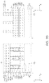
- FIG. 1 is a plan diagram illustrating a semiconductor device according to an exemplary embodiment of the present inventive concept
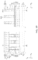
- FIG. 2A is a cross-sectional diagram illustrating a semiconductor device according to an exemplary embodiment of the present inventive concept
- FIGS. 2B, 2C, 2D and 2E are enlarged cross-sectional diagrams illustrating a portion of a semiconductor device according to an exemplary embodiment of the present inventive concept
- FIG. 3A is a cross-sectional diagram illustrating a semiconductor device according to an exemplary embodiment of the present inventive concept
- FIGS. 3B, 3C, 3D and 3E are enlarged cross-sectional diagrams illustrating a portion of a semiconductor device according to an exemplary embodiment of the present inventive concept
- FIG. 4A is a cross-sectional diagram illustrating a semiconductor device according to an exemplary embodiment of the present inventive concept
- FIGS. 4B, 4C, 4D and 4E are enlarged cross-sectional diagrams illustrating a portion of a semiconductor device according to an exemplary embodiment of the present inventive concept
- FIG. 5 is a cross-sectional diagram illustrating a semiconductor device according to an exemplary embodiment of the present inventive concept
- FIG. 6 is a cross-sectional diagram illustrating a semiconductor device according to an exemplary embodiment of the present inventive concept
- FIG. 7 is a cross-sectional diagram illustrating a semiconductor device according to an exemplary embodiment of the present inventive concept.
- FIGS. 8, 9, 10, 11, 12, 13, 14, 15, 16, 17, 18, 19, 20, 21, 22, 23, 24, 25 and 26 are cross-sectional diagrams illustrating a method of manufacturing a semiconductor device according to an exemplary embodiment of the present inventive concept.
- FIG. 1 is a plan diagram illustrating a semiconductor device according to an exemplary embodiment of the present inventive concept.
- a first conductive structure 12 and a second conductive structure 72 on the first conductive structure 12 may be disposed.
- memory cell structures MC 1 and MC 2 may be disposed between the first conductive structure 12 and the second conductive structure 72 .
- the memory cell structures MC 1 and MC 2 may include various patterns such as a quadrangular shape (e.g., a square shape, a rectangular shape, and the like), or a circular shape, and the like.
- the memory cell structures MC 1 and MC 2 may include a switching material pattern 26 and a data storage material pattern 36 .
- each of the switching material pattern 26 and the data storage material pattern 36 may have a square shape.
- the data storage material pattern 36 may be disposed on a central portion of an upper surface of the switching material pattern 26 .
- FIG. 2A is a cross-sectional diagram illustrating cross-sectional surfaces of the semiconductor device taken along lines I-I′ and II-II′ in FIG. 1 according to an exemplary embodiment of the present inventive concept
- FIGS. 2B and 2C are enlarged diagrams illustrating region ‘A’ illustrated in FIG. 2A according to an exemplary embodiment of the present inventive concept.
- the base structure 3 may include a semiconductor substrate 6 and a circuit region 9 on the semiconductor substrate 6 .
- the semiconductor substrate 6 may be, for example, a substrate formed of a semiconductor material such as silicon.
- the circuit region 9 may be a region in which a circuit required for driving memory cells is disposed.
- a plurality of the first conductive structures 12 may be disposed in parallel to each other on the base structure 3 .
- Each of the first conductive structures 12 may have a linear shape extending in a first direction X, and the first conductive structures 12 may be spaced apart from each other in a second direction Y and may be disposed side by side.
- Each of the second conductive structures 72 may have a linear shape extending in the second direction Y, and the second conductive structures 72 may be spaced apart from each other in the first direction X and may be disposed in parallel to each other.
- Each of the third conductive structures 112 may have a linear shape extending in the first direction X, and the third conductive structures 112 may be spaced apart from each other in the second direction Y and may be disposed side by side.
- the first direction X and the second direction Y may be substantially perpendicular to each other, and may be in parallel to an upper surface 6 s of the semiconductor substrate 6 .
- one of the first conductive structure 12 and the second conductive structure 72 may be a word line, and the other may be a bit line.
- the third conductive structure 112 may be a word line.
- first conductive structures 12 , the second conductive structures 72 , and the third conductive structures 112 may be referred to as first conducive lines, second conductive lines, and third conductive lines, respectively.
- a gap-fill insulating pattern 20 may be disposed on each of lateral surfaces of the first conductive structure 12 .
- the gap-fill insulating pattern 20 may be disposed between the first conductive structures 12 , and may have a linear shape extending in the first direction X.
- the gap-fill insulating pattern 20 may be include an insulating material such as silicon oxide, and the like.
- the memory cell structures MC 1 and MC 2 may be disposed between the first conductive structure 12 and the second conductive structure 72 and between the second conductive structure 72 and the third conductive structure 112 .
- the memory cell structures MC 1 and MC 2 may include a first memory cell structure MC 1 disposed between the first conductive structure 12 and the second conductive structure 72 , and a second memory cell structure MC 2 disposed between the second conductive structure 72 and the third conductive structure 112 .
- the memory cell structures MC 1 and MC 2 may have a stacked structure in a third direction Z.
- the memory structures MC 1 and MC 2 may form a two-stack structure.
- the third direction Z may be substantially perpendicular to the first and second directions X and Y, and may be substantially perpendicular to the upper surface 6 s of the substrate 6 .
- a basic unit of the memory cell structures MC 1 and MC 2 will be described, and a two-stack structure of the memory cell structures MC 1 and MC 2 will be described.
- the first memory cell structure MC 1 may include a switching structure 22 on the first conductive structure 12 , a data storage structure 32 on the switching structure 22 , and an upper conductive pattern 44 on the data storage structure 32 .
- the second memory cell structure MC 2 may include a switching structure 22 on the second conductive structure 72 , a data storage structure 32 on the switching structure 22 , and an upper conductive pattern 44 on the data storage structure 32 .
- the switching structure 22 may include a lower conductive pattern 24 on the first conductive structure 12 .
- the switching structure 22 may include the switching material pattern 26 on the lower conductive pattern 24 , and an intermediate conductive pattern 28 on the switching material pattern 26 .
- the lower conductive pattern 24 may be disposed between the first conductive structure 12 and the switching material pattern 26 .
- the switching material pattern 26 may be disposed between the lower conductive pattern 24 and the intermediate conductive pattern 28 .
- the intermediate conductive pattern 28 may be disposed between the switching material pattern 26 and the data storage structure 32 .
- the data storage structure 32 may include a lower electrode pattern 34 on the intermediate conductive pattern 28 . Further the data storage structure 32 may include the data storage material pattern 36 on the lower electrode pattern 34 , and an upper electrode pattern 38 on the data storage material pattern 36 .
- the lower electrode pattern 34 may be disposed between the intermediate conductive pattern 28 and the data storage material pattern 36 .
- the data storage material pattern 36 may be disposed between the lower electrode pattern 34 and the upper electrode pattern 38 .
- the upper electrode pattern 38 may be disposed between the data storage material pattern 36 and the upper conductive pattern 44 .
- the data storage material pattern 36 may be disposed on a central portion of an upper surface of the lower electrode pattern 34 .
- the lower electrode pattern 34 may have a width in the second direction Y that is greater than that of the data storage material pattern 36 .
- the upper electrode pattern 36 may be disposed on a central portion of an upper surface of the data storage material pattern 36 .
- a first insulating pattern 70 and a second insulating pattern 72 may be disposed.
- the first insulating pattern 70 may be disposed on a lateral surface of each of the first memory cell structures MC 1 and fill a region between the first conductive structure 12 and the second conductive structure 72
- a second insulating pattern 71 may be disposed on a lateral surface of each of the second memory cell structures MC 2 and fill a region between the second conductive structure 72 and the third conductive structure 112 .
- the first insulating pattern 70 may surround lateral surfaces of the first memory cell structures MC 1 .
- the second insulating pattern 71 may surround lateral surfaces of the second memory cell structures MC 2 .
- the first and second insulating patterns 70 and 71 may be formed of an insulating material such as silicon oxide, silicon nitride, or the like.
- the switching structure 22 may form an ovonic threshold switching device.
- the switching material pattern 26 may be formed of a chalcogenide-based ovonic threshold switching material which may maintain an amorphous phase when the semiconductor device operates.
- the switching material pattern 26 may include an alloy material including at least two or more elements from among As, S, Se, Te, and/or Ge, or may include an additional element (e.g., elements Si, N, or the like) which may maintain an amorphous phase at a relatively higher temperature in addition to the above-mentioned alloy material.
- the switching material pattern 26 may be formed of at least one of an alloy material including Te, As, Ge, and Si, an alloy material including Ge, Te, and Pb, an alloy material including Ge, Se, and Te, an alloy material including Al, As, and Te, an alloy material including Se, As, Ge, and Si, an alloy material including Se, As, Ge, and C, an alloy material including Se, Te, Ge, and Si, an alloy material including Ge, Sb, Te, and Sc, an alloy material including Ge, Bi, Te, and Se, an alloy material including Ge, As, Sb, and Se, an alloy material including Ge, As, Bi, and Te, and/or an alloy material including Ge, As, Bi, and Se.
- the lower conductive pattern 24 , the intermediate conductive pattern 28 , and the upper conductive pattern 44 may include a carbon layer or a material layer including carbon.
- the material layer including carbon may include a metal element such as tungsten (W) and carbon (C).
- the material layer including carbon may include other metal elements such as titanium (Ti), tantalum (Ta), ruthenium (Ru), or the like, in addition to tungsten (W).
- the material layer including carbon may further include elements such as nitride (N), boron (B), or the like, in addition to carbon (C) and metal elements.
- the data storage material pattern 36 may include of a chalcogenide-based phase change memory material, a phase of which may change from an amorphous phase having high resistivity to a crystalline phase having low resistivity or from a crystalline phase to an amorphous phase in accordance with a temperature and a time of heating the data storage material pattern 36 by an applied current.
- the data storage material pattern 36 may be configured as a phase change memory material such as a chalcogenide material including Ge, Sb, and/or Te, and the like.
- the data storage material pattern 36 may be a phase change memory material including at least one of Te or Se and at least one of Ge, Sb, Bi, Pb, Sn, As, S, Si, P, O, N, or In.
- the data storage material pattern 36 may be formed of a data storage material which may store data in a different manner, instead of a phase change memory material.
- the lower electrode pattern 34 and the upper electrode pattern 38 may be formed of a conductive material such as tungsten, or the like.
- the lower electrode pattern 34 and the upper electrode pattern 38 may be formed of a conductive material including W, TiN, TiAlN, TaN, WN, MoN, TiSiN, TiCN, TiBN, ZrSiN, WSiN, WBN, ZrAlN, MoAlN, TaSiN, TaAlN, TiON, TiAlON, WON, and TaON, or combinations thereof.
- the memory cell structures MC 1 and MC 2 may be referred to as memory cell regions, and the memory cell regions may include a first memory cell region and a second memory cell region adjacent to each other.
- the memory cell regions may be provided to describe a distance relationship between the first memory cell region and the second memory cell region adjacent to each other, and may be the same as the memory cell structures MC 1 and MC 2 .
- the first memory cell region (e.g., a first memory cell structure MC 1 ) may include a first switching material pattern, a first data storage material pattern on the first switching material pattern, a first upper electrode pattern on the first data storage material pattern, and a first upper conductive pattern on the first upper electrode pattern.
- the second memory cell region (e.g., another first memory cell structure) may include a second switching material pattern, a second data storage material pattern on the second switching material pattern, a second upper electrode pattern on the second data storage material pattern, and a second upper conductive pattern on the second upper electrode pattern.
- a lateral surface of an upper region of the first data storage material pattern and a lateral surface of an upper region of the second data storage material pattern that opposes the lateral surface of an upper region of the first data storage material pattern may be spaced apart from each other by a first distance D 1 a.
- a lateral surface of the first upper conductive pattern and a lateral surface of the second upper conductive pattern that opposes the lateral surface of the first upper conductive pattern may be spaced apart from each other by a second distance D 2 a.
- a lateral surface of the first upper electrode pattern and a lateral surface of the second upper electrode pattern that opposes the lateral surface of the first upper electrode pattern may be spaced apart from each other by a third distance D 3 a.
- the first distance D 1 a may be less than a minimum value of the second distance D 2 a
- a maximum value of the third distance D 3 a may be substantially the same as a minimum value of the second distance D 2 a.
- the descriptions off the first to third distances D 1 a , D 2 a , and D 3 a may be applied in both the first and second directions X and Y.
- the present inventive concept is not limited thereto.
- the first to third distances D 1 a , D 2 a , and D 3 a may change in accordance with a modified exemplary embodiment of the present inventive concept.
- each of the lower conductive pattern 24 , the switching material pattern 26 , the intermediate conductive pattern 28 , the lower electrode pattern 34 , the data storage material pattern 36 , the upper electrode pattern 38 , and the upper conductive pattern 44 may have a sloped lateral surface, and a width of an upper portion of the first memory cell structure MC 1 is less than a width of a lower portion of the first memory cell structure MC 1 .
- the present inventive concept is not limited thereto.
- the data storage material pattern 36 may include an upper region adjacent to an interfacial surface between the data storage material pattern 36 and the upper electrode pattern 38 .
- the interfacial surface may be where the upper surface of the data storage material 36 contacts the lower surface of the upper electrode pattern 38 .
- the data storage material 36 may include a lower region adjacent to an interfacial surface between the data storage material pattern 36 and the lower electrode pattern 34 , and an intermediate region between the upper region and the lower region.
- the interfacial surface may be where the lower surface of the data storage material 36 contacts the upper surface of the lower electrode pattern 38 .
- the data storage material pattern 36 may have a shape in which a width of the upper region and a width of the lower region may be greater than a width of the intermediate region.
- the data storage material pattern 36 may have lateral surfaces that are partially recessed such that the intermediate region may have an inwardly recessed shape.
- the data storage material pattern 36 may have a concave shape.
- the present inventive concept is not limited thereto.
- lateral surfaces of each of the switching material pattern 26 , the lower conductive pattern 24 , the intermediate conductive pattern 28 , and the lower electrode pattern 34 may be substantially coplanar with one another.
- a width of the switching material pattern 26 may be referred to as a first width W 1 .
- the data storage material pattern 36 may have a width W 2 a of in the upper region, and may have a width W 2 b of in the lower region.
- a maximum value of the width W 2 b of the lower region may be less than a minimum value of the first width W 1 .
- the maximum value of the width W 2 b may be adjacent the lower surface of the data storage material 36
- the minimum value of the first width W 1 may be adjacent an upper surface of the switching material pattern 26 .
- the upper electrode pattern 38 may have a third width W 3 , and a maximum value of the third width W 3 may be less than the width W 2 b of the lower region of the data storage material 36 .
- the maximum value of the third width W 3 may be adjacent a lower surface of the upper electrode pattern 38 .
- the upper conductive pattern 44 may have a fourth width W 4 , and a maximum value of the fourth width W 4 may be less than the width W 2 b of the lower region and may be substantially the same as a minimum value of the third width W 3 .
- the maximum value of the fourth width W 4 may be adjacent a lower surface of the upper conductive pattern 44 .
- the descriptions of the first to fourth widths W 1 to W 4 may be applied in both the first and second directions X and Y.
- a leaning defect of the memory cell structures may be prevented such that durability and reliability of the semiconductor device may increases.
- Layers disposed on an upper portion of the data storage material pattern 36 may be etched, and a protective spacer may be disposed on lateral surfaces of the etched layers.
- a width of the protective spacer By adjusting a width of the protective spacer, the widths W 2 a and W 2 b of the upper region and the lower region of the data storage material pattern 36 may be adjusted.
- a residue of the conductive material including tungsten (W) and a residue of the data storage material may be deposited on the protective spacer, and when a cleaning process is performed, a residue of the data storage material may be effectively removed along with the protective spacer. Accordingly, damage to the memory cell structures MC 1 and MC 2 caused during an etching process and a cleaning process may be prevented.
- first spacer structures may be disposed between the first memory cell structure MC 1 and the first insulating pattern 70 in the second direction Y.
- Second spacer structures may be disposed between the first memory cell structures MC 1 and the first insulating pattern 70 in the first direction X.
- the first and second spacer structures may be formed of an insulating material such as silicon oxide, silicon nitride, or the like.
- the first spacer structures 63 a may include a first spacer 65 a adjacent to the memory cell structures MC 1 and MC 2 and a second spacer 67 a adjacent to the first insulating pattern 70 .
- the first spacer 65 a may extend in the third direction Z from the lower electrode pattern 34 , and may be disposed on a first lateral surface 36 S_ 1 of the data storage material pattern 36 , a first lateral surface 38 S_ 11 of the upper electrode pattern 38 , and a first lateral surface 44 S_ 11 of the upper conductive pattern 44 .
- the first spacer 65 a may have a substantially uniform thickness and may have a first spacer width WS 1 .
- the first lateral surface 38 S_ 1 of the upper electrode pattern 38 and the first lateral surface 44 S_ 1 of the upper conductive pattern 44 may be substantially coplanar with each other.
- the first spacer 65 a may cover an edge of an upper surface of the storage material pattern 36 .
- the first spacer 65 a may have a curved shape to surround an end of an upper surface of the data storage material pattern 36 .
- a sum of widths of edges of both side of the upper surface of the storage material pattern 36 , covered by the first spacer 65 a may be substantially the same as a difference between the width W 2 a of the upper region and the third width W 3 .
- the second spacer 67 a may extend in the third direction Z from the first conductive structure 12 , and may be disposed on an external lateral surface of the first spacer 65 a and a first lateral surface 22 S_ 1 of the switching structure 22 .
- the second spacer 67 a may have a substantially uniform thickness and may have a second spacer width WS 2 .
- the second spacer 67 a may have a curved shape to surround an end of an upper surface of the data storage material pattern 36 .
- the second spacer 67 a may cover an edge of an upper surface of the first conductive structure 12 .
- a sum of width of edges of both sides of the upper surface of the first conductive structure 12 , covered by the second spacer 67 a may be substantially the same as a difference between a width of the first conductive line 12 and the first width W 1 .
- a difference between a width of the first conductive line 12 and the first width W 1 may be substantially the same as twice the second spacer width WS 2 .
- second spacer structures 63 b may include a third spacer 65 b and a fourth spacer 67 b .
- the third spacer 65 b may be on the memory cell structures MC 1 and MC 2
- the fourth spacer 67 b may be adjacent to the second insulating pattern 71 .
- the third spacer 65 b may extend from the lower electrode pattern 34 in the third direction Z, and may be disposed on a second lateral surface 36 S_ 2 of the data storage material pattern 36 , a second lateral surface 38 S_ 2 of the upper electrode pattern 38 , and a second lateral surface 44 S_ 2 of the upper conductive pattern 44 .
- the third spacer 65 b may have a substantially uniform thickness and may have a first spacer width WS 1 .
- the second lateral surface 38 S_ 2 of the upper electrode pattern 38 and the second lateral surface 44 S_ 2 of the upper conductive pattern 44 may be substantially coplanar with each other.
- the third spacer 65 b may cover an edge of an upper surface of the data storage material pattern 36 .
- the third spacer 65 b may have a curved shape to surround an end of the upper surface of the data storage material pattern 36 .
- the third spacer 65 b may cover an edge of an upper surface of the lower electrode pattern 34 .
- the fourth spacer 67 b may extend from the first conductive structure 12 in the third direction Z, and may be disposed on an external lateral surface of the third spacer 65 b and a second lateral surface 22 S_ 12 of the switching structure 22 .
- the fourth spacer 67 b may have a substantially uniform thickness and may have a second spacer width WS 2 .
- the fourth spacer 67 b may have a curved shape to surround an end of an upper surface of the data storage material pattern 36 .
- the fourth spacer 67 b may cover an edge of an upper surface of the first conductive structure 12 .
- the second spacer structures 63 b may include a portion extending further than the first spacer structures 63 a . Accordingly, a height of each of the second spacer structures 63 b in the third direction Z may be greater than a height of each of the first spacer structures 63 a in the third direction Z. Accordingly, the third spacer 65 b may extend further than the first spacer 65 a in the third direction Z and may be in contact with a lateral surface of the second conductive structure 72 , and the fourth spacer 67 b may extend further than the second spacer 67 a and may be disposed on a lateral surface of the second conductive structure 72 .
- the first spacer width WS 1 and the second spacer width WS 2 may not be limited to the examples illustrated in the diagram, and may be different.
- first spacer 65 a and the third spacer 65 b may be referred to as a first region
- second spacer 67 a and the fourth spacer 67 b may be referred to as a second region.
- FIGS. 2D and 2E are enlarged cross-sectional diagrams illustrating a portion of a semiconductor device according to an exemplary embodiment of the present inventive concept, and the semiconductor device further includes a protective spacer.
- FIG. 2D illustrates a region corresponding to region “A” illustrated in FIG. 2A
- FIG. 2E illustrates a region corresponding to region “A- 1 ” illustrated in FIG. 2A .
- first spacer structures 163 a may include a first spacer 165 a adjacent to the first memory cell structure MC 1 , a second spacer 167 a adjacent to the first insulating pattern 70 , and a first protective spacer 161 a disposed between the first spacer 165 a and the first memory cell structure MC 1 .
- the first protective spacer 161 a may extend from the data storage material pattern 36 in the third direction Z, and may be disposed on a first lateral surface 38 S_ 1 of the upper electrode pattern 38 and a first lateral surface 44 S_ 1 of the upper conductive pattern 44 .
- the first spacer 165 a may be disposed on an external lateral surface of the first protective spacer 161 a and a first lateral surface 36 S_ 1 of the data storage material pattern 36 .
- the first protective spacer 161 a may be disposed between the first spacer 165 a and the upper conductive pattern 44 .
- the first spacer 165 a may be directly in contact with the first lateral surface 36 S_ 1 of the data storage material pattern 36 .
- the first spacer 165 a may cover an edge of an upper surface of the lower electrode pattern 34 .
- the second spacer 167 a may extend from the first conductive structure 12 in the third direction Z, and may be disposed on an external lateral surface of the first spacer 165 a and a first lateral surface 22 S_ 1 of the switching structure 22 .
- the second spacer 167 a may cover an edge of an upper surface of the first conductive structure 12 .
- second spacer structures 163 b may include a third spacer 165 b adjacent to the first memory cell structure MC 1 , a fourth spacer 167 b adjacent to the first insulating pattern 70 , and a second protective spacer 161 b disposed between the third spacer 165 b and the first memory cell structure MC 1 .
- the second protective spacer 161 b may extend from the data storage material pattern 36 in the third direction Z, and may be disposed on a second lateral surface 38 S_ 2 of the upper electrode pattern 38 and a second lateral surface 44 S_ 2 of the upper conductive pattern 44 .
- the third spacer 165 b may be disposed on an external lateral surface of the second protective spacer 161 b and a second lateral surface 36 S_ 2 of the data storage material pattern 36 .
- the second protective spacer 161 b may be disposed between the third spacer 165 b and the upper conductive pattern 44 .
- the third spacer 165 b may be directly in contact with a second lateral surface 36 S_ 2 of the data storage material pattern 36 .
- the third spacer 165 b may cover an edge of an upper surface of the lower electrode pattern 34 .
- the fourth spacer 167 b may extend from the first conductive structure 12 in the third direction Z, and may be disposed on an external lateral surface of the third spacer 165 b and a second lateral surface 22 S_ 2 of the switching structure 22 .
- the fourth spacer 167 b may cover an edge of an upper surface of the first conductive structure 12 .
- the first and second protective spacers 161 a and 161 b may be referred to as protective spacers.
- the second memory cell structure MC 2 may have a structure formed by rotating the first memory cell structure MC 1 by, for example, 90 degrees on a plane. Accordingly, in FIG.
- the second memory cell structure MC 2 in the region marked by line may have a structure substantially the same as a structure of the first memory cell structure MC 1 in the region marked by line II-II′, and the second memory cell structure MC 2 in the region marked by line II-II′ may have may have a structure substantially the same as a structure of the first memory cell structure MC 1 in the region marked by line I-I′.
- FIGS. 3A to 7 In the description below, one or more exemplary embodiments of the present inventive concept will be described with reference to FIGS. 3A to 7 . In the descriptions of one or more exemplary embodiments of the present inventive concept, only modified portions of the semiconductor device described in the aforementioned exemplary embodiment of the present inventive concept with reference to FIGS. 2A to 2E will be described. Thus, other elements and portions of the modified exemplary embodiments of the present inventive concept may be understood from the aforementioned exemplary embodiment described with reference to FIGS. 2A to 2E unless otherwise indicated.
- FIG. 3A is a cross-sectional diagram illustrating cross-sectional surfaces of the semiconductor device taken along lines I-I′ and II-II′ in FIG. 1 according to an exemplary embodiment of the present inventive concept
- FIGS. 3B and 3C are enlarged diagrams illustrating region “B” illustrated in FIG. 3A according to an exemplary embodiment of the present inventive concept.
- a maximum value of a third distance D 3 b may be smaller than a minimum value of a second distance D 2 a , and a minimum value of the third distance D 3 b may be substantially the same as a first distance D 1 a.
- the description of the third distance D 3 b may be applied in both the first and second directions X and Y.
- a first spacer 65 c may cover an edge of an upper surface of an upper electrode pattern 38 a .
- the first spacer 65 c may have a curved shape to surround an end of an upper surface of the upper electrode pattern 38 a.
- a sum of widths of edges of both sides of the upper surface of the upper electrode pattern 38 a , covered by the first spacer 65 c may be substantially the same as a difference between a third width W 3 a and a fourth width W 4 .
- a second spacer 67 c may have a curved shape to surround an end of an upper surface of the upper electrode pattern 38 a.
- first spacer 65 c and the second spacer 67 c may also be applied to a third spacer 65 d and a fourth spacer 67 d.
- the upper electrode pattern 38 a may have the third width W 3 a , and a minimum value of the third width W 3 a may be substantially the same as a width W 2 a of an upper region.
- a minimum value of the third width W 3 a may be greater than a maximum value of the fourth width W 4 .
- the description of the third width W 3 a may be applied in both the first and second directions X and Y.
- a first lateral surface 38 a S_ 1 of the upper electrode pattern 38 a and a first lateral surface 36 S_ 1 of a data storage material pattern 36 may be substantially coplanar with each other.
- the first lateral surface 38 a S_ 1 of the upper electrode pattern 38 a and the first lateral surface 36 S_ 1 of a data storage material pattern 36 may be self-aligned.
- FIGS. 3D and 3E are enlarged cross-sectional diagrams illustrating a portion of a semiconductor device, according to an exemplary embodiment of the present inventive concept, further including a protective spacer.
- FIG. 3D illustrates a region corresponding to region “B” illustrated in FIG. 3A
- FIG. 3E illustrates a region corresponding to region “B- 1 ” illustrated in FIG. 3A .
- first spacer structures 163 c may include a first spacer 165 c adjacent to a first memory cell structure MC 1 , a second spacer 167 c adjacent to a first insulating pattern 70 , and a first protective spacer 161 c disposed between the first spacer 165 c and the first memory cell structure MC 1 .
- the first protective spacer 161 c may extend from the upper electrode pattern 38 a in the third direction Z, and may be disposed on a first lateral surface 44 S_ 1 of the upper conductive pattern 44 .
- the first spacer 165 c may be disposed on an external lateral surface of the first protective spacer 161 c and a first lateral surface 36 S_ 1 of the data storage material pattern 36 .
- the first protective spacer 161 c may be disposed between the first spacer 165 c and the upper conductive pattern 44 .
- the first spacer 165 c may cover an edge of an upper surface of the lower electrode pattern 34 .
- the second spacer 167 c may extend from the first conductive structure 12 in the third direction Z, and may be disposed on an external lateral surface of the first spacer 165 e and a first lateral surface 22 S_ 1 of a switching structure 22 .
- the second spacer 167 c may cover an edge of an upper surface of the first conductive structure 12 .
- first spacer 165 c the second spacer 167 c , and the first protective spacer 161 c may also be applied to a third spacer 165 d , a fourth spacer 167 d , and a second protective spacer 161 d (in, e.g., FIG. 3E ).
- FIG. 4A is a cross-sectional diagram illustrating cross-sectional surfaces of a semiconductor device taken along lines I-I′ and II-II′ in FIG. 1 according to an exemplary embodiment of the present inventive concept.
- FIGS. 4B and 4C are enlarged diagrams illustrating region “C” illustrated in FIG. 4A according to an exemplary embodiment of the present inventive concept.
- a minimum value of a second distance D 2 b may be greater than a first distance D 1 a.
- a minimum value of a third distance D 3 b may be greater than the third distance D 3 b .
- a maximum value of the third distance D 3 b may be less than a minimum value of the second distance D 2 b.
- the descriptions of the second distance D 2 a and the third distance D 3 b may be applied in both the first and second directions X and Y.
- a first spacer 65 e may cover an edge of an upper surface of a data storage material pattern 36 and an edge of an upper surface of an upper electrode pattern 38 b .
- the first spacer 65 e may have a curved shape to surround an end of an upper surface of the data storage material pattern 36 and an end of an upper surface of the upper electrode pattern 38 b.
- a sum of widths of edges of both sides of the upper surface of the data storage material pattern 36 and widths of edges of both sides of an upper surface of the upper electrode pattern 38 b may be substantially the same as a difference between a width W 2 a of an upper region and a fourth width W 4 a.
- a second spacer 67 e may have a curved shape to surround an end of an upper surface of the data storage material pattern 36 and an end of an upper surface of the upper electrode pattern 38 b.
- first spacer 65 e and the second spacer 67 e may also be applied to a third spacer 65 f and a fourth spacer 67 f.
- an upper electrode pattern 38 b may have a third width W 3 b , and a maximum value of the third width W 3 b may be less than a width W 2 a of the upper region of the data storage material pattern 36 .
- an upper conductive pattern 44 a may have a fourth width W 4 a , and a maximum value of the fourth width W 4 a may be less than a minimum value of the third width W 3 b .
- a maximum value of the third width W 3 b may be less than the width W 2 a of the upper region of the data storage material pattern 36 .
- the descriptions of the third width W 3 b and the fourth width W 4 a may be applied in both the first and second directions X and Y.
- a first lateral surface 44 a S_ 1 of the upper conductive pattern 44 a , a first lateral surface 38 b S_ 1 of the upper electrode pattern 38 b , and a first lateral surface 36 S_ 1 of the data storage material pattern 36 may not be coplanar with one another.
- FIGS. 4D and 4E are enlarged cross-sectional diagrams illustrating a portion of a semiconductor device, according to an exemplary embodiment of the present inventive concept, further including protective spacers.
- first spacer structures 163 e may include a first spacer 165 e adjacent to first memory cell structures MC 1 , a second spacer 167 e adjacent to a first insulating pattern 70 , and a first internal protective spacer 161 e and a first external protective spacer 161 ee disposed between the first spacer 165 e and the first memory cell structures MC 1 .
- the first internal protective spacer 161 e may extend from an upper electrode pattern 38 b in the third direction Z, and may be disposed on a first lateral surface 44 a S_ 1 of the upper conductive pattern 44 a.
- the first external protective spacer 161 ee may extend from a data storage material pattern 36 in the third direction Z, and may be disposed on the first lateral surface 44 a S_ 1 of the upper conductive pattern 44 a and on a first lateral surface 38 b S_ 1 of the upper electrode pattern 38 b.
- the first internal protective spacer 161 e may be disposed between the first external protective spacer 161 ee and the upper conductive pattern 44 a .
- the first external protective spacer 161 ee may be disposed between the first internal protective spacer 161 e and the first spacer 165 e .
- the first lateral surface 44 a S_ 1 of the upper conductive pattern 44 a may be directly in contact with the first internal protective spacer 161 e .
- the first lateral surface 38 b S_ 1 of the upper electrode pattern 38 b may be directly in contact with the first external protective spacer 161 ee.
- the first spacer 165 e may be disposed on an external lateral surface of the first external protective spacer 161 ee and a first lateral surface 36 S_ 1 of the data storage material pattern 36 .
- the first spacer 165 e may cover an edge of an upper surface of a lower electrode pattern 34 .
- the second spacer 167 e may extend from a first conductive structure 12 in the third direction Z, and may be disposed on an external lateral surface of the first spacer 165 e and a first lateral surface 22 S_ 1 of a switching structure 22 .
- the second spacer 167 e may cover an edge of an upper surface of the first conductive structure 12 .
- first spacer 165 e the second spacer 167 e , the first internal protective spacer 161 e , and the first external protective spacer 161 ee may also be applied to a third spacer 165 f , a fourth spacer 167 f , a second internal protective spacer 161 f , and a second external protective spacer 161 ff.
- FIGS. 5 to 7 are cross-sectional diagrams illustrating cross-sectional surfaces of a semiconductor device taken along lines I-I′ and II-II′ in FIG. 1 according to an exemplary embodiment of the present inventive concept.
- each of a second memory cell structure MC 2 in a region marked by line I-I′ in FIG. 5 and a first memory cell structure MC 1 in a region marked by line II-II′ in FIG. 5 may have a structure different from a structure of each of the memory cell structures in FIG. 2A .
- a width of a switching structure 222 in the first direction X may be greater than a width of the switching structure 222 in the second direction Y.
- the switching structure 222 may include a switching material pattern 226 , and a width of the switching material pattern 226 in the first direction X may be greater than width of the switching material pattern 226 in the second direction Y.
- a width of a data storage structure 232 in the first direction X may be greater than a width of the data storage structure 232 in the second direction Y.
- the data storage structure 232 may include a data storage material pattern 236 , and a width of the data storage material pattern 236 in the first direction X may be greater than a width of the data storage material pattern 236 in the second direction Y.
- a first distance D 1 a between upper regions of the data storage material patterns 236 in the second direction Y may be greater than a first distance D 1 a ′ between upper regions of the data storage material patterns 236 in the first direction X.
- a second distance D 2 a between upper conductive patterns 244 adjacent to each other in the second direction Y may be greater than a second distance D 2 a ′ between upper conductive patterns 244 adjacent to each other in the first direction X.
- a third distance D 3 a between upper electrode patterns 238 adjacent to each other in the second direction Y may be greater than a third distance D 3 a ′ between upper electrode patterns 238 adjacent to each other in the first direction X.
- the first distance D 1 a ′ may be less than a minimum value of the second distance D 2 a ′, and a maximum value of the third distance D 3 a ′ may be substantially the same as a minimum value of the second distance D 2 a′.
- each of the second memory cell structure MC 2 in a region marked by line I-I′ in FIG. 6 and the first memory cell structure MC 1 in a region marked by line II-II′ in FIG. 6 may have a structure different from a structure of each of the memory cell structures in FIG. 3A .
- a width of a data storage structure 232 a in the first direction X may be greater than a width of the data storage structure 232 a in the second direction Y.
- the data storage structure 232 a may include a data storage material pattern 236 , and a width of the data storage material pattern 236 in the first direction X may be greater than a width of the data storage material pattern 236 in the second direction Y.
- a first distance D 1 a between the data storage material patterns 236 adjacent to each other in the second direction Y may be greater than a first distance D 1 a ′ between the data storage material patterns 236 adjacent to each other in the first direction X.
- a second distance D 2 a between the upper conductive patterns 244 adjacent to each other in the second direction Y may be greater than a second direction D 2 a ′ between the upper conductive patterns 244 adjacent to each other in the first direction X.
- a third distance D 3 b between upper electrode patterns 238 adjacent to each other in the second direction Y may be greater than a third distance D 3 b ′ between upper electrode patterns 238 adjacent to each other in the first direction X.
- a maximum value of the third distance D 3 b ′ may be greater than a minimum value of the second distance D 2 a ′, and a minimum value of the third distance D 3 b ′ may be substantially the same as the first distance D 1 a′.
- each of the second memory cell structure MC 2 in a region marked by line I-I′ in FIG. 7 and the first memory cell structure MC 1 in a region marked by line II-II′ in FIG. 7 may have a structure different from the structure of each of the memory cell structures in FIG. 4A .
- a width of a data storage structure 232 b in the first direction X may be greater than a width of the data storage structure 232 b in the second direction Y.
- the data storage structure 232 b may include a data storage material pattern 236 , and a width of the data storage material pattern 236 in the first direction X may be greater than a width of the data storage material pattern 236 in the second direction Y.
- a first distance D 1 a between the data storage material patterns 236 adjacent to each other in the second direction V may be greater than a first distance D 1 a ′ between the data storage material patterns 236 adjacent to each other in the first direction X.
- a second distance D 2 b between the upper conductive patterns 244 adjacent to each other in the second direction Y may be greater than a second distance D 2 b ′ in the first direction X.
- a third distance D 3 c between upper electrode patterns 238 adjacent to each other in the second direction V may be greater than a third distance D 3 c ′ between upper electrode patterns 238 adjacent to each other in the first direction X.
- the second distance D 2 b ′ may be greater than the first distance D 1 a ′.
- a minimum value of the second distance D 2 b ′ may be greater than a minimum value of the first distance D 1 a′.
- a minimum value of the third distance D 3 c ′ may be greater than the first distance D 1 a ′, and a maximum value of the third distance D 3 c ′ may be less than a minimum value of the second direction D 2 b′.
- Each of the switching structure 22 , the data storage structure 32 , and the upper conductive pattern 44 included in the memory cell structures MC 1 and MC 2 of the semiconductor device described with reference to FIGS. 1 to 7 above may have a sloped lateral surface, a width of an upper portion of which is narrower than a width of a lower portion, in accordance with an aspect ratio.
- the present inventive concept is not limited thereto.
- FIGS. 8 to 27 are cross-sectional diagrams illustrating regions taken along lines I-I′ and II-II′ in FIG. 1 according to an exemplary embodiment of the present inventive.
- a base structure 3 may include a semiconductor substrate 6 and a lower circuit region 9 on the semiconductor substrate 6 .
- the lower circuit region 9 may be a peripheral circuit region.
- a first conducive structure 12 extending in the first direction X may be disposed on the base structure 3 .
- a gap-fill insulating pattern 20 may be formed on lateral surfaces of the first conductive structure 12 .
- the gap-fill insulating pattern 20 may be formed of an insulating material such as silicon oxide, or the like.
- a plurality of layers in parallel to an upper surface 6 s of the semiconductor substrate 6 and extending in the first and second directions X and Y may be formed on the first conductive structure 12 and the gap-fill insulating pattern 20 .
- the plurality of layers may include a lower conductive layer 124 , a switching material layer 126 , an intermediate conductive layer 128 , a lower electrode layer 134 , a data storage material layer 136 , an upper electrode layer 138 , and an upper conductive layer 144 stacked in that order.
- First mask patterns 51 each having a linear shape extending in the first direction X may be formed on an upper surface of the upper conductive layer 144 .
- the first mask patterns 51 may include a polysilicon layer 55 and a silicon oxide layer 59 stacked in that order.
- partial regions of the upper conductive layer 144 and the upper electrode layer 138 may be removed using an etching process. Regions which are not removed by the etching process may remain as an upper conductive line 144 ′ and an upper electrode line 138 ′. Each of the upper conductive line 144 ′ and the upper electrode line 138 ′ may have a linear shape extending in the first direction X. As a partial region of the upper electrode layer 138 on the data storage material layer 136 is removed, a portion of an upper surface of the data storage material layer 136 may be exposed.
- a first protective spacer 161 a covering a lateral surface of the upper conductive line 144 ′, a lateral surface of the upper electrode line 138 ′, and lateral surfaces of the first mask patterns 51 may be formed.
- the first protective spacer 161 a may extend from a portion of the upper surface of the data storage material layer 136 in the third direction Z.
- the first protective spacer 161 a may be formed of an insulating material such as silicon oxide, silicon nitride, or the like.
- the first protective spacer 161 a may be formed using atomic layer deposition (ALD).
- the first protective spacer 161 a may be formed by the atomic layer deposition method at a temperature of about 0° C. or higher and 250° C. or lower approximately.
- a width of the first protective spacer 161 a may be varied according to an exemplary embodiment of the present inventive concept.
- an acid-based cleaning process or an alkali-based cleaning process may be performed.
- a partial region of the data storage material layer 136 may be removed using an etching process.
- a region which is not removed by the etching process may remain as a data storage material line 136 ′.
- the data storage material line 136 ′ may have a linear shape extending in the first direction X.
- a partial region of the data storage material layer 136 is removed, a portion of an upper surface of the lower electrode layer 134 may be exposed.
- the data storage material line 136 ′ disposed in a lower portion of the upper conductive line 144 ′ may have a width greater than a width of the upper conductive line 144 ′.
- a width of the data storage material line 136 ′ may be greater than a width of the upper conductive line 144 ′ by a width WP 1 of the first protective spacer.
- a residue of the data storage material may be deposited on an external lateral surface of the first protective spacer 161 a .
- the residue of the data storage material may also be removed. Accordingly, the residue of the data storage material may remain on the lower electrode layer 134 , the data storage material line 136 ′, and the upper conductive line 144 ′ such that damage to the pattern caused during the cleaning process may be prevented.
- the cleaning process may be performed under a condition of acid of pH0 to pH4 or alkali of pH6 to pH11. In an exemplary embodiment of the present inventive concept, the first protective spacer 161 a may not be removed.
- the first protective spacer 161 a may remain on a lateral surface of the upper conductive line 144 ′ and a lateral surface of the upper electrode line 138 ′ while the residue of the data storage material is deposited on the external lateral surface.
- an exemplary embodiment of the present inventive concept is not limited thereto.
- the residue of the data storage material deposited on the external surface of the first protective spacer 161 a may be removed through the cleaning process.
- a first spacer 65 a extending from the lower electrode layer 134 in the third direction Z and the first direction X may be formed.
- the first spacer 65 a may be disposed on a lateral surface of the data storage material line 136 ′, a lateral surface of the upper electrode line 138 ′, and a lateral surface of the upper conductive line 144 ′.
- the first spacer 65 a may cover an edge of an upper surface of the data storage material line 136 ′.
- the first spacer 65 a may have a curved shape to surround an end of an upper surface of the data storage material line 136 ′.
- the first spacer 65 a may have a substantially uniform thickness.
- the first spacer 65 a may be formed through atomic layer deposition (ALD).
- the first spacer 65 a may be formed of an insulating material such as silicon oxide, silicon nitride, or the like.
- partial regions of the lower electrode layer 134 , the intermediate conductive layer 128 , the switching material layer 126 , and the lower conductive layer 124 may be removed using an etching process. Regions which are not removed by the etching process may remain as a lower electrode line 134 ′, an intermediate conductive line 128 ′, a switching material line 126 ′, and a lower conductive line 124 ′.
- Each of the lower electrode line 134 ′, the intermediate conductive line 128 ′, the switching material line 126 ′, and the lower conductive line 124 ′ may have a linear shape extending in the first direction X. As the partial regions of the lower electrode layer 134 , the intermediate conductive layer 128 , the switching material layer 126 , and the lower conductive layer 124 are removed, an edge of an upper surface of the first conductive structure 12 and an upper surface of the gap-fill insulating pattern 20 may be exposed.
- a second spacer 67 a extending from an edge of an upper surface of the first conductive structure 12 in the third direction Z may be formed.
- the second spacer 67 a may be disposed on a lateral surface of the lower conductive line 124 ′, a lateral surface, of the switching material line 126 ′, a lateral surface of the intermediate conductive line 128 ′, and a lateral surface of the lower electrode line 134 ′.
- the second spacer 67 a may be disposed on an external lateral surface of the first spacer 65 a.
- the second spacer 67 a may have a curved shape to surround an end of an upper portion of the data storage material line 136 ′.
- the second spacer 67 a may have a substantially uniform thickness.
- the second spacer 67 a may be formed through atomic layer deposition (ALD).
- the second spacer 67 a may be formed of an insulating material such as silicon oxide, silicon nitride, or the like.
- a first insulating pattern 70 extending from the gap-fill insulating pattern 20 in the third direction Z may be formed.
- the first insulating pattern 70 may be in contact with an external lateral surface of the second spacer 67 a .
- the first insulating pattern 70 may be formed of an insulating material such as silicon oxide, silicon nitride, or the like.
- the first mask patterns 51 , an upper portion of the first spacer 65 a , an upper portion of the second spacer 67 a , and an upper portion of the first insulating pattern 70 may be removed.
- An upper surface of the upper conductive line 144 ′ may be exposed.
- a second preliminary conductive layer 72 ′ covering the exposed upper surface of the upper conductive line 144 ′ and an upper surface of the first insulating pattern 70 may be formed.
- the second preliminary conductive layer 72 ′ may be in parallel to the upper surface 6 s of the semiconductor substrate 6 and may extend in the first and second directions X and Y.
- a structure of a semiconductor device according to an exemplary embodiment of the present inventive concept may be manufactured by changing an etching process and a process of forming a spacer.
- a partial region of the upper conductive layer 144 may be removed using an etching process, and a protective spacer may be formed.
- the protective spacer may be formed.
- the protective spacer may be formed through a cleaning process, a partial region of an upper electrode layer 138 may be removed, and another protective spacer may be formed.
- second mask patterns 151 each having a linear shape extending in the second direction Y may be formed on an upper surface of a second preliminary conductive layer 72 ′.
- the second mask patterns 151 may include a poly silicon layer 155 and a silicon oxide layer 159 stacked in that order.
- partial regions of the second preliminary conductive layer 72 ′, the upper conductive line 144 ′, and the upper electrode line 138 ′ may be removed. Accordingly, a second conductive structure 72 , an upper conductive pattern 44 , and an upper electrode pattern 38 may be formed. A portion of an upper surface of the data storage material line 136 ′ may be exposed through the etching process.
- a second protective spacer 161 b covering a lateral surface of the upper conductive pattern 44 , a lateral surface of the upper electrode pattern 38 , and a lateral surface of the second mask patterns 151 may be formed.
- the second protective spacer 161 b may extend from a portion of an upper surface of the data storage material line 136 ′ in the third direction Z.
- the second protective spacer 161 b may be formed of an insulating material such as silicon oxide, silicon nitride, or the like.
- the second protective spacer 161 b may be formed through atomic layer deposition.
- the second protective spacer 161 b may be formed using an atomic layer deposition method at a temperature of about 0° C. or higher and 250° C. or lower approximately.
- a width of the second protective spacer 161 b may be vary in an exemplary embodiment of the present inventive concept.
- an acid-based cleaning process or an alkali-based cleaning process may be performed.
- a partial region of the data storage material line 136 ′ may be removed using an etching process. As the partial region of the data storage material line 136 ′ having a linear shape is removed, a data storage material pattern 36 may be formed. A portion of an upper surface of the lower electrode line 134 ′ may be exposed through the etching process.
- the data storage material pattern 36 disposed on a lower portion of the upper conductive pattern 44 may have a width greater than a width of the upper conductive pattern 44 .
- a width of the data storage material pattern 36 may be greater than a width of the upper conductive pattern 44 by a width WP 2 of the second protective spacer.
- a residue of a data storage material may be deposited on an external lateral surface of the second protective spacer 161 b .
- the residue of the data storage material may be effectively removed as the second protective spacer 161 b is removed. Accordingly, the residue of the data storage material may remain on the lower electrode line 134 ′, the data storage material pattern 36 , and the upper conductive pattern 44 such that damage to the pattern, which may occur in the cleaning process, may be prevented.
- the second protective spacer 161 b may not be removed. Accordingly, the second protective spacer 161 b may remain on a lateral surface of the upper conductive pattern 44 and a lateral surface of the upper electrode pattern 38 while the residue of the data storage material is deposited on an external lateral surface of the second protective spacer 161 b .
- the present inventive concept is not limited thereto. The residue of the data storage material deposited on the external lateral surface of the second protective spacer 161 b may be removed through a cleaning process.
- a third spacer 65 b extending from the intermediate conductive line 134 ′ in the third direction Z and the first direction X may be formed.
- the third spacer 65 b may be disposed on a lateral surface of the data storage material pattern 36 , a lateral surface of the upper electrode pattern 38 , and a lateral surface of the upper conductive pattern 44 .
- the third spacer 65 b may include a portion extending further than the first spacer 65 a in the third direction Z and may be disposed on a lateral surface of the second conductive structure 72 .
- the third spacer 65 b may cover an edge of an upper surface of the data storage material pattern 36 .
- the third spacer 65 b may have a curved shape to surround an end of an upper surface of the data storage material pattern 36 .
- the third spacer 65 b may have a substantially uniform thickness and may have a first spacer width WS 1 .
- the third spacer 65 b may be formed through atomic layer deposition.
- the third spacer 65 b may be formed of an insulating material such as silicon oxide, silicon nitride, or the like.
- Partial regions of the lower electrode line 134 ′, the intermediate conductive line 128 ′, the switching material line 126 ′, and the lower conductive line 124 ′ may be removed. Accordingly, the lower electrode pattern 34 , the intermediate conductive pattern 28 , the switching material pattern 26 , and the lower conductive pattern 24 may be formed.
- An upper surface of the first conductive structure 12 and an upper surface of the gap-fill insulating pattern 20 may be exposed through the etching process.
- a fourth spacer 67 b extending from an upper surface of the first conductive structure 12 in the third direction Z may be formed.
- the fourth spacer 67 b may be disposed on a lateral surface of the lower conductive pattern 24 , a lateral surface of the switching material pattern 26 , a lateral surface of the intermediate conductive pattern 28 , and a lateral surface of the lower electrode pattern 34 .
- the fourth spacer 67 b may be disposed on an external lateral surface of the third spacer 65 b .
- the fourth spacer 67 b may include a portion extending further than the second spacer 67 a in the third direction Z and may be disposed on a lateral surface of the second conductive structure 72 .
- the fourth spacer 67 b may have a curved shape to surround an end of an upper portion of the data storage material pattern 36 .
- the fourth spacer 67 b may have a substantially uniform thickness.
- fourth spacer 67 b may be formed through atomic layer deposition.
- the fourth spacer 67 b may be formed of an insulating material such as silicon oxide, silicon nitride, or the like.
- a first insulating pattern 70 extending from the first conductive structure 12 in the third direction Z may be formed.
- the first insulating pattern 70 may be in contact with an external lateral surface of the fourth spacer 67 b .
- the first insulating pattern 70 may be formed of an insulating material such as silicon oxide, silicon nitride, or the like.
- the second mask patterns 151 , an upper portion of the third spacer 65 b , an upper portion of the fourth spacer 67 b , and an upper portion of the first insulating pattern 70 may be removed. An upper surface of the first insulating pattern 70 may be exposed.
- a structure of a semiconductor device according to a modified exemplary embodiment of the present inventive concept may be manufactured by changing an etching process and a process of forming a spacer.
- partial regions of the second preliminary conductive layer 72 ′ and the upper conductive line 144 ′ may be removed using an etching process.
- a protective spacer may be formed, and partial regions of the upper electrode line 138 ′ and the data storage material line 136 may be removed using an etching process. Accordingly, a modified exemplary embodiment of the exemplary embodiment illustrated in FIGS. 3A and 3B may be provided.
- partial regions of the second preliminary conductive layer 72 ′ and the upper conductive line 144 ′ may be removed using an etching process.
- a protective spacer may be formed, and the protective spacer may be removed through a cleaning process.
- a partial region of the upper electrode line 138 ′ may be removed, and another protective spacer may be formed. Accordingly, a modified exemplary embodiment of the exemplary embodiment illustrated FIGS. 4A and 4B may be provided.
- a leaning defect of the semiconductor device pattern may be prevented.
- the spacers which may remove residual metals remaining in the etching process, may be formed, damage to the semiconductor device caused by the residual metals may be prevented.
Landscapes
- Engineering & Computer Science (AREA)
- Manufacturing & Machinery (AREA)
- Physics & Mathematics (AREA)
- Condensed Matter Physics & Semiconductors (AREA)
- General Physics & Mathematics (AREA)
- Computer Hardware Design (AREA)
- Microelectronics & Electronic Packaging (AREA)
- Power Engineering (AREA)
- Semiconductor Memories (AREA)
Applications Claiming Priority (2)
| Application Number | Priority Date | Filing Date | Title |
|---|---|---|---|
| KR1020190088807A KR20210012079A (ko) | 2019-07-23 | 2019-07-23 | 정보 저장 물질 패턴을 포함하는 반도체 소자 |
| KR10-2019-0088807 | 2019-07-23 |
Publications (2)
| Publication Number | Publication Date |
|---|---|
| US20210028360A1 US20210028360A1 (en) | 2021-01-28 |
| US11217748B2 true US11217748B2 (en) | 2022-01-04 |
Family
ID=74189454
Family Applications (1)
| Application Number | Title | Priority Date | Filing Date |
|---|---|---|---|
| US16/807,245 Active 2040-03-19 US11217748B2 (en) | 2019-07-23 | 2020-03-03 | Semiconductor device including a data storage material pattern |
Country Status (3)
| Country | Link |
|---|---|
| US (1) | US11217748B2 (ko) |
| KR (1) | KR20210012079A (ko) |
| CN (1) | CN112310147A (ko) |
Cited By (1)
| Publication number | Priority date | Publication date | Assignee | Title |
|---|---|---|---|---|
| US11393977B2 (en) * | 2019-08-29 | 2022-07-19 | Samsung Electronics Co., Ltd. | Semiconductor device including vertical structures and a method of manufacturing the same |
Families Citing this family (1)
| Publication number | Priority date | Publication date | Assignee | Title |
|---|---|---|---|---|
| KR20210069164A (ko) | 2019-12-02 | 2021-06-11 | 삼성전자주식회사 | 가변 저항 메모리 소자 및 이의 제조 방법 |
Citations (10)
| Publication number | Priority date | Publication date | Assignee | Title |
|---|---|---|---|---|
| JP2010225872A (ja) | 2009-03-24 | 2010-10-07 | Toshiba Corp | 半導体装置及びその製造方法 |
| JP2011071302A (ja) | 2009-09-25 | 2011-04-07 | Toshiba Corp | 不揮発性記憶装置の製造方法および不揮発性記憶装置 |
| US8394667B2 (en) | 2010-07-14 | 2013-03-12 | Micron Technology, Inc. | Methods of forming memory cells, and methods of patterning chalcogenide-containing stacks |
| US8686387B2 (en) | 2011-06-10 | 2014-04-01 | Kabushiki Kaisha Toshiba | Semiconductor memory device and method for manufacturing the same |
| US8729667B2 (en) | 2012-01-23 | 2014-05-20 | Kabushiki Kaisha Toshiba | Non-volatile memory device and method of manufacturing the same |
| US20150287916A1 (en) | 2014-04-03 | 2015-10-08 | Micron Technology, Inc. | Semiconductor structures including multi-portion liners and related methods |
| US9484196B2 (en) | 2014-02-25 | 2016-11-01 | Micron Technology, Inc. | Semiconductor structures including liners comprising alucone and related methods |
| US20170271581A1 (en) * | 2016-03-18 | 2017-09-21 | Dong-Jun Seong | Semiconductor memory devices |
| US20170364306A1 (en) | 2016-06-17 | 2017-12-21 | SK Hynix Inc. | Electronic device and method for fabricating the same |
| US20180158869A1 (en) * | 2016-04-15 | 2018-06-07 | Taiwan Semiconductor Manufacturing Company Ltd. | Semiconductor structure |
Family Cites Families (8)
| Publication number | Priority date | Publication date | Assignee | Title |
|---|---|---|---|---|
| KR102171267B1 (ko) * | 2014-01-28 | 2020-10-28 | 삼성전자 주식회사 | 랜딩 패드를 구비하는 반도체 소자 |
| US9806129B2 (en) * | 2014-02-25 | 2017-10-31 | Micron Technology, Inc. | Cross-point memory and methods for fabrication of same |
| KR102316317B1 (ko) * | 2015-06-05 | 2021-10-22 | 삼성전자주식회사 | 반도체 소자 및 이의 제조 방법 |
| KR102453349B1 (ko) * | 2016-02-25 | 2022-10-07 | 삼성전자주식회사 | 가변 저항 메모리 장치 및 이의 제조 방법 |
| KR102463023B1 (ko) * | 2016-02-25 | 2022-11-03 | 삼성전자주식회사 | 가변 저항 메모리 장치 및 이의 제조 방법 |
| US9842882B1 (en) * | 2016-05-18 | 2017-12-12 | SK Hynix Inc. | Electronic device |
| KR102323249B1 (ko) * | 2017-03-28 | 2021-11-08 | 삼성전자주식회사 | 정보 저장 패턴을 포함하는 반도체 소자 |
| KR102396119B1 (ko) * | 2017-09-15 | 2022-05-11 | 에스케이하이닉스 주식회사 | 전자 장치 및 그 제조 방법 |
-
2019
- 2019-07-23 KR KR1020190088807A patent/KR20210012079A/ko not_active Application Discontinuation
-
2020
- 2020-03-03 US US16/807,245 patent/US11217748B2/en active Active
- 2020-07-08 CN CN202010652460.8A patent/CN112310147A/zh active Pending
Patent Citations (10)
| Publication number | Priority date | Publication date | Assignee | Title |
|---|---|---|---|---|
| JP2010225872A (ja) | 2009-03-24 | 2010-10-07 | Toshiba Corp | 半導体装置及びその製造方法 |
| JP2011071302A (ja) | 2009-09-25 | 2011-04-07 | Toshiba Corp | 不揮発性記憶装置の製造方法および不揮発性記憶装置 |
| US8394667B2 (en) | 2010-07-14 | 2013-03-12 | Micron Technology, Inc. | Methods of forming memory cells, and methods of patterning chalcogenide-containing stacks |
| US8686387B2 (en) | 2011-06-10 | 2014-04-01 | Kabushiki Kaisha Toshiba | Semiconductor memory device and method for manufacturing the same |
| US8729667B2 (en) | 2012-01-23 | 2014-05-20 | Kabushiki Kaisha Toshiba | Non-volatile memory device and method of manufacturing the same |
| US9484196B2 (en) | 2014-02-25 | 2016-11-01 | Micron Technology, Inc. | Semiconductor structures including liners comprising alucone and related methods |
| US20150287916A1 (en) | 2014-04-03 | 2015-10-08 | Micron Technology, Inc. | Semiconductor structures including multi-portion liners and related methods |
| US20170271581A1 (en) * | 2016-03-18 | 2017-09-21 | Dong-Jun Seong | Semiconductor memory devices |
| US20180158869A1 (en) * | 2016-04-15 | 2018-06-07 | Taiwan Semiconductor Manufacturing Company Ltd. | Semiconductor structure |
| US20170364306A1 (en) | 2016-06-17 | 2017-12-21 | SK Hynix Inc. | Electronic device and method for fabricating the same |
Cited By (1)
| Publication number | Priority date | Publication date | Assignee | Title |
|---|---|---|---|---|
| US11393977B2 (en) * | 2019-08-29 | 2022-07-19 | Samsung Electronics Co., Ltd. | Semiconductor device including vertical structures and a method of manufacturing the same |
Also Published As
| Publication number | Publication date |
|---|---|
| US20210028360A1 (en) | 2021-01-28 |
| KR20210012079A (ko) | 2021-02-03 |
| CN112310147A (zh) | 2021-02-02 |
Similar Documents
| Publication | Publication Date | Title |
|---|---|---|
| US7642622B2 (en) | Phase changeable memory cells and methods of forming the same | |
| US7667221B2 (en) | Phase change memory devices and methods for fabricating the same | |
| US9118003B2 (en) | Variable resistance memory devices and method of forming the same | |
| US11094745B2 (en) | Variable resistance memory device and method of fabricating the same | |
| US8592790B2 (en) | Phase-change random access memory device and method of manufacturing the same | |
| US11245073B2 (en) | Switching element, variable resistance memory device, and method of manufacturing the switching element | |
| US11217748B2 (en) | Semiconductor device including a data storage material pattern | |
| US20180166502A1 (en) | Semiconductor device including a line pattern having threshold switching devices | |
| US20180019281A1 (en) | Variable resistance memory devices and methods of fabricating the same | |
| KR20170085409A (ko) | 가변 저항 메모리 소자 및 이의 제조 방법 | |
| US8765521B2 (en) | Variable resistance memory devices and methods of manufacturing the same | |
| US11276821B2 (en) | Variable resistance memory device | |
| US8853660B2 (en) | Semiconductor memory devices having lower and upper interconnections, selection components and memory components | |
| US10971548B2 (en) | Variable resistance memory device including symmetrical memory cell arrangements and method of forming the same | |
| US8686385B2 (en) | Phase-change random access memory device and method of manufacturing the same | |
| US11502130B2 (en) | Variable resistance memory device and method of fabricating the same | |
| US11393977B2 (en) | Semiconductor device including vertical structures and a method of manufacturing the same | |
| US10833124B2 (en) | Semiconductor devices including data storage patterns | |
| US11387410B2 (en) | Semiconductor device including data storage material pattern | |
| US10916584B2 (en) | Semiconductor device including a data storage pattern and a method of manufacturing the same | |
| US11177320B2 (en) | Variable resistance memory device and method of fabricating the same | |
| KR20100088406A (ko) | 상변화 기억 소자 및 그 제조방법 | |
| US20130171798A1 (en) | Method of manufacturing phase-change random access memory device | |
| KR20120087713A (ko) | 상변화 메모리 장치의 제조방법 | |
| KR20130087197A (ko) | 상변화 메모리 장치의 제조방법 |
Legal Events
| Date | Code | Title | Description |
|---|---|---|---|
| AS | Assignment |
Owner name: SAMSUNG ELECTRONICS CO., LTD., KOREA, REPUBLIC OF Free format text: ASSIGNMENT OF ASSIGNORS INTEREST;ASSIGNORS:KIM, YOUNGTAK;PARK, SANGJINE;LEE, WONJUN;AND OTHERS;REEL/FRAME:051988/0617 Effective date: 20200120 |
|
| FEPP | Fee payment procedure |
Free format text: ENTITY STATUS SET TO UNDISCOUNTED (ORIGINAL EVENT CODE: BIG.); ENTITY STATUS OF PATENT OWNER: LARGE ENTITY |
|
| STPP | Information on status: patent application and granting procedure in general |
Free format text: DOCKETED NEW CASE - READY FOR EXAMINATION |
|
| STPP | Information on status: patent application and granting procedure in general |
Free format text: NON FINAL ACTION MAILED |
|
| STPP | Information on status: patent application and granting procedure in general |
Free format text: NOTICE OF ALLOWANCE MAILED -- APPLICATION RECEIVED IN OFFICE OF PUBLICATIONS |
|
| STPP | Information on status: patent application and granting procedure in general |
Free format text: PUBLICATIONS -- ISSUE FEE PAYMENT VERIFIED |
|
| STCF | Information on status: patent grant |
Free format text: PATENTED CASE |