US10566200B2 - Method of fabricating transistors, including ambient oxidizing after etchings into barrier layers and anti-reflecting coatings - Google Patents
Method of fabricating transistors, including ambient oxidizing after etchings into barrier layers and anti-reflecting coatings Download PDFInfo
- Publication number
- US10566200B2 US10566200B2 US15/944,550 US201815944550A US10566200B2 US 10566200 B2 US10566200 B2 US 10566200B2 US 201815944550 A US201815944550 A US 201815944550A US 10566200 B2 US10566200 B2 US 10566200B2
- Authority
- US
- United States
- Prior art keywords
- layer
- semiconductor substrate
- thickness
- oxide
- forming
- Prior art date
- Legal status (The legal status is an assumption and is not a legal conclusion. Google has not performed a legal analysis and makes no representation as to the accuracy of the status listed.)
- Active
Links
Images


Classifications
-
- H—ELECTRICITY
- H10—SEMICONDUCTOR DEVICES; ELECTRIC SOLID-STATE DEVICES NOT OTHERWISE PROVIDED FOR
- H10D—INORGANIC ELECTRIC SEMICONDUCTOR DEVICES
- H10D30/00—Field-effect transistors [FET]
- H10D30/01—Manufacture or treatment
- H10D30/021—Manufacture or treatment of FETs having insulated gates [IGFET]
- H10D30/0221—Manufacture or treatment of FETs having insulated gates [IGFET] having asymmetry in the channel direction, e.g. lateral high-voltage MISFETs having drain offset region or extended-drain MOSFETs [EDMOS]
-
- H01L21/266—
-
- H—ELECTRICITY
- H10—SEMICONDUCTOR DEVICES; ELECTRIC SOLID-STATE DEVICES NOT OTHERWISE PROVIDED FOR
- H10P—GENERIC PROCESSES OR APPARATUS FOR THE MANUFACTURE OR TREATMENT OF DEVICES COVERED BY CLASS H10
- H10P30/00—Ion implantation into wafers, substrates or parts of devices
- H10P30/20—Ion implantation into wafers, substrates or parts of devices into semiconductor materials, e.g. for doping
- H10P30/22—Ion implantation into wafers, substrates or parts of devices into semiconductor materials, e.g. for doping using masks
-
- H01L29/6659—
-
- H—ELECTRICITY
- H10—SEMICONDUCTOR DEVICES; ELECTRIC SOLID-STATE DEVICES NOT OTHERWISE PROVIDED FOR
- H10D—INORGANIC ELECTRIC SEMICONDUCTOR DEVICES
- H10D30/00—Field-effect transistors [FET]
- H10D30/01—Manufacture or treatment
- H10D30/021—Manufacture or treatment of FETs having insulated gates [IGFET]
- H10D30/0223—Manufacture or treatment of FETs having insulated gates [IGFET] having source and drain regions or source and drain extensions self-aligned to sides of the gate
- H10D30/0227—Manufacture or treatment of FETs having insulated gates [IGFET] having source and drain regions or source and drain extensions self-aligned to sides of the gate having both lightly-doped source and drain extensions and source and drain regions self-aligned to the sides of the gate, e.g. lightly-doped drain [LDD] MOSFET or double-diffused drain [DDD] MOSFET
-
- H—ELECTRICITY
- H10—SEMICONDUCTOR DEVICES; ELECTRIC SOLID-STATE DEVICES NOT OTHERWISE PROVIDED FOR
- H10D—INORGANIC ELECTRIC SEMICONDUCTOR DEVICES
- H10D30/00—Field-effect transistors [FET]
- H10D30/60—Insulated-gate field-effect transistors [IGFET]
- H10D30/601—Insulated-gate field-effect transistors [IGFET] having lightly-doped drain or source extensions, e.g. LDD IGFETs or DDD IGFETs
- H10D30/603—Insulated-gate field-effect transistors [IGFET] having lightly-doped drain or source extensions, e.g. LDD IGFETs or DDD IGFETs having asymmetry in the channel direction, e.g. lateral high-voltage MISFETs having drain offset region or extended drain IGFETs [EDMOS]
-
- H—ELECTRICITY
- H10—SEMICONDUCTOR DEVICES; ELECTRIC SOLID-STATE DEVICES NOT OTHERWISE PROVIDED FOR
- H10D—INORGANIC ELECTRIC SEMICONDUCTOR DEVICES
- H10D30/00—Field-effect transistors [FET]
- H10D30/60—Insulated-gate field-effect transistors [IGFET]
- H10D30/64—Double-diffused metal-oxide semiconductor [DMOS] FETs
- H10D30/65—Lateral DMOS [LDMOS] FETs
-
- H—ELECTRICITY
- H10—SEMICONDUCTOR DEVICES; ELECTRIC SOLID-STATE DEVICES NOT OTHERWISE PROVIDED FOR
- H10D—INORGANIC ELECTRIC SEMICONDUCTOR DEVICES
- H10D64/00—Electrodes of devices having potential barriers
- H10D64/20—Electrodes characterised by their shapes, relative sizes or dispositions
- H10D64/27—Electrodes not carrying the current to be rectified, amplified, oscillated or switched, e.g. gates
- H10D64/311—Gate electrodes for field-effect devices
- H10D64/411—Gate electrodes for field-effect devices for FETs
- H10D64/511—Gate electrodes for field-effect devices for FETs for IGFETs
- H10D64/514—Gate electrodes for field-effect devices for FETs for IGFETs characterised by the insulating layers
- H10D64/516—Gate electrodes for field-effect devices for FETs for IGFETs characterised by the insulating layers the thicknesses being non-uniform
-
- H—ELECTRICITY
- H10—SEMICONDUCTOR DEVICES; ELECTRIC SOLID-STATE DEVICES NOT OTHERWISE PROVIDED FOR
- H10D—INORGANIC ELECTRIC SEMICONDUCTOR DEVICES
- H10D84/00—Integrated devices formed in or on semiconductor substrates that comprise only semiconducting layers, e.g. on Si wafers or on GaAs-on-Si wafers
- H10D84/01—Manufacture or treatment
- H10D84/0123—Integrating together multiple components covered by H10D12/00 or H10D30/00, e.g. integrating multiple IGBTs
- H10D84/0126—Integrating together multiple components covered by H10D12/00 or H10D30/00, e.g. integrating multiple IGBTs the components including insulated gates, e.g. IGFETs
- H10D84/0144—Manufacturing their gate insulating layers
-
- H—ELECTRICITY
- H10—SEMICONDUCTOR DEVICES; ELECTRIC SOLID-STATE DEVICES NOT OTHERWISE PROVIDED FOR
- H10D—INORGANIC ELECTRIC SEMICONDUCTOR DEVICES
- H10D84/00—Integrated devices formed in or on semiconductor substrates that comprise only semiconducting layers, e.g. on Si wafers or on GaAs-on-Si wafers
- H10D84/01—Manufacture or treatment
- H10D84/02—Manufacture or treatment characterised by using material-based technologies
- H10D84/03—Manufacture or treatment characterised by using material-based technologies using Group IV technology, e.g. silicon technology or silicon-carbide [SiC] technology
- H10D84/038—Manufacture or treatment characterised by using material-based technologies using Group IV technology, e.g. silicon technology or silicon-carbide [SiC] technology using silicon technology, e.g. SiGe
-
- H—ELECTRICITY
- H10—SEMICONDUCTOR DEVICES; ELECTRIC SOLID-STATE DEVICES NOT OTHERWISE PROVIDED FOR
- H10D—INORGANIC ELECTRIC SEMICONDUCTOR DEVICES
- H10D84/00—Integrated devices formed in or on semiconductor substrates that comprise only semiconducting layers, e.g. on Si wafers or on GaAs-on-Si wafers
- H10D84/80—Integrated devices formed in or on semiconductor substrates that comprise only semiconducting layers, e.g. on Si wafers or on GaAs-on-Si wafers characterised by the integration of at least one component covered by groups H10D12/00 or H10D30/00, e.g. integration of IGFETs
- H10D84/82—Integrated devices formed in or on semiconductor substrates that comprise only semiconducting layers, e.g. on Si wafers or on GaAs-on-Si wafers characterised by the integration of at least one component covered by groups H10D12/00 or H10D30/00, e.g. integration of IGFETs of only field-effect components
- H10D84/83—Integrated devices formed in or on semiconductor substrates that comprise only semiconducting layers, e.g. on Si wafers or on GaAs-on-Si wafers characterised by the integration of at least one component covered by groups H10D12/00 or H10D30/00, e.g. integration of IGFETs of only field-effect components of only insulated-gate FETs [IGFET]
- H10D84/8314—Integrated devices formed in or on semiconductor substrates that comprise only semiconducting layers, e.g. on Si wafers or on GaAs-on-Si wafers characterised by the integration of at least one component covered by groups H10D12/00 or H10D30/00, e.g. integration of IGFETs of only field-effect components of only insulated-gate FETs [IGFET] the IGFETs characterised by having gate insulating layers with different properties
-
- H—ELECTRICITY
- H10—SEMICONDUCTOR DEVICES; ELECTRIC SOLID-STATE DEVICES NOT OTHERWISE PROVIDED FOR
- H10D—INORGANIC ELECTRIC SEMICONDUCTOR DEVICES
- H10D84/00—Integrated devices formed in or on semiconductor substrates that comprise only semiconducting layers, e.g. on Si wafers or on GaAs-on-Si wafers
- H10D84/80—Integrated devices formed in or on semiconductor substrates that comprise only semiconducting layers, e.g. on Si wafers or on GaAs-on-Si wafers characterised by the integration of at least one component covered by groups H10D12/00 or H10D30/00, e.g. integration of IGFETs
- H10D84/82—Integrated devices formed in or on semiconductor substrates that comprise only semiconducting layers, e.g. on Si wafers or on GaAs-on-Si wafers characterised by the integration of at least one component covered by groups H10D12/00 or H10D30/00, e.g. integration of IGFETs of only field-effect components
- H10D84/83—Integrated devices formed in or on semiconductor substrates that comprise only semiconducting layers, e.g. on Si wafers or on GaAs-on-Si wafers characterised by the integration of at least one component covered by groups H10D12/00 or H10D30/00, e.g. integration of IGFETs of only field-effect components of only insulated-gate FETs [IGFET]
- H10D84/836—Integrated devices formed in or on semiconductor substrates that comprise only semiconducting layers, e.g. on Si wafers or on GaAs-on-Si wafers characterised by the integration of at least one component covered by groups H10D12/00 or H10D30/00, e.g. integration of IGFETs of only field-effect components of only insulated-gate FETs [IGFET] comprising EDMOS
Definitions
- transistors having a relatively low specific resistance In many applications, it is desirable to fabricate transistors having a relatively low specific resistance.
- some field-effect-transistors such as drain-extended metal-oxide-semiconductor (DEMOS) transistors, increasing the oxide thickness over part of the gate oxide may lower specific resistance.
- DEMOS drain-extended metal-oxide-semiconductor
- a method to fabricate a transistor comprises: forming a first dielectric layer on a semiconductor substrate; depositing a barrier layer on the first dielectric layer; depositing an anti-reflective coating on the barrier layer; depositing a photoresist layer; exposing a pattern in the photoresist layer to radiation; etching the photoresist layer according to the pattern to provide an opening in the photoresist layer; etching a portion of the anti-reflective coating below the opening in the photoresist layer; etching a portion of the barrier layer below the opening to expose a portion of the first dielectric layer; providing an ambient oxidizing agent after etching the portion of the barrier layer below the opening to grow an oxide region; removing the barrier layer after providing the ambient oxidizing agent; implanting dopants into the semiconductor substrate after removing the barrier layer; removing the first dielectric layer after implanting dopants into the semiconductor substrate; and forming a second dielectric layer after removing the first dielectric layer
- a method to fabricate a transistor comprises: forming a sacrificial oxide layer on a semiconductor substrate; depositing a silicon nitride layer on the sacrificial oxide layer; depositing an anti-reflective coating on the silicon nitride layer; depositing a photoresist layer; exposing a pattern in the photoresist layer to radiation; etching the photoresist layer according to the pattern to provide an opening in the photoresist layer; etching a portion of the anti-reflective coating below the opening; etching a portion of the silicon nitride layer below the opening to expose a portion of the sacrificial oxide layer; and growing an oxide region on the exposed portion of the sacrificial oxide layer; removing the silicon nitride layer after growing the oxide region; implanting dopants into the semiconductor substrate after removing the silicon nitride layer; removing the sacrificial oxide layer after implanting dopants into the
- a method to fabricate a transistor comprises: forming a sacrificial oxide layer on a semiconductor substrate; depositing a silicon nitride layer on the sacrificial oxide layer; depositing a photoresist layer; exposing a pattern in the photoresist layer to radiation; etching the photoresist layer according to the pattern to provide an opening in the photoresist layer; etching a portion of the silicon nitride layer below the opening to expose a portion of the sacrificial oxide layer; growing an oxide region of at least 400 angstroms thick on the exposed portion of the sacrificial oxide layer; removing the silicon nitride layer after growing the oxide region; implanting dopants into the semiconductor substrate after removing the silicon nitride layer to form a drain region in the semiconductor substrate; removing the sacrificial oxide layer after implanting dopants into the semiconductor substrate; and forming a gate oxide layer on the semiconductor substrate after removing the
- FIG. 1 shows a transistor in accordance with various examples
- FIG. 2 shows a semiconductor substrate with several layers in accordance with various examples
- FIG. 3 shows a silicon substrate after etching in accordance with various examples
- FIG. 4 shows a silicon substrate with an oxide region in accordance with various examples
- FIG. 5 shows a process flow in accordance with various examples.
- FIG. 6 shows two transistors in accordance with various examples.
- a method to fabricate transistors includes growing a thick oxide below the transistor gate, where the process steps can be incorporated into a standard bipolar complementary-metal-oxide-semiconductor (BiCMOS) process flow.
- BiCMOS bipolar complementary-metal-oxide-semiconductor
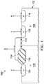
- FIG. 1 shows a cross-sectional view of an illustrative transistor 100 , not drawn to scale.
- the illustrative transistor 100 is a DEMOS transistor.
- Formed in a semiconductor substrate 102 is a drain region 104 and a source region 106 .
- the semiconductor substrate 102 is a silicon crystal
- the illustrative transistor 100 is an n-type DEMOS transistor, where the drain region 104 and the source region 106 are each highly doped n-type regions.
- the source region 106 is formed within a lightly doped p-type well 108 , and the drain region 104 is extended by way of the lightly doped n-type region 110 .
- a dielectric layer 112 is formed on the semiconductor substrate 102 .
- the dielectric layer 112 is usually silicon dioxide, and the dielectric layer 112 will be referred to as a gate oxide layer 112 .
- a gate 114 is formed over the gate oxide layer 112 .
- the gate 114 may comprise polysilicon.
- An oxide region 116 is grown on and into the semiconductor substrate 102 .
- the oxide region 116 is adjacent to the drain region 104 and is below the gate 114 , and the oxide region 116 is thicker than the dielectric layer 112 .
- the oxide region 116 may comprise silicon dioxide.
- the presence of the oxide region 116 provides a lift-up to the gate 114 .
- a highly doped p-type region 118 serves as a body contact for the illustrative transistor 100 .
- a channel current of majority carriers (e.g., electrons for an n-type channel) flows from the source region 106 to the drain region 104 .
- the presence of the oxide region 116 affects the path of the channel current.
- the relatively large depth of the oxide region 116 into the channel forces the majority carriers of the channel current to accelerate as they move underneath the oxide region 116 and toward the drain region 104 .
- the acceleration of the majority carriers helps to reduce the specific resistance of the illustrative transistor 100 .
- the oxide region 116 may be employed in other types of transistors, such as for example a double-diffusion metal-oxide-semiconductor (DMOS) transistor, as well as other types of lateral or vertical transistors.
- DMOS double-diffusion metal-oxide-semiconductor
- other semiconductor devices may be formed in the semiconductor substrate 102 and coupled to the illustrative transistor 100 to realize various circuits.
- a silicon trench isolation (STI) region is formed around the illustrative transistor 100 to provide electrical isolation from other semiconductor devices.
- FIG. 2 shows a cross-sectional view (not drawn to scale) of the semiconductor substrate 102 and several layers formed during part of a process flow according to embodiments.
- a sacrificial dielectric layer 204 is formed over the semiconductor substrate 102 .
- the sacrificial dielectric layer 204 typically comprises silicon dioxide, and will be referred to as a sacrificial oxide layer 204 .
- a barrier layer 206 typically silicon nitride, is deposited on the sacrificial oxide layer 204 .
- a bottom antireflective coating (BARC) 208 is deposited on the barrier layer 206 , and a photoresist layer 210 is deposited on the BARC 208 .
- BARC bottom antireflective coating
- the photoresist layer 210 is exposed to radiation according to an illumination pattern defined by a mask (not shown).
- the pattern illuminated on the photoresist layer 210 defines an opening for growing the oxide region 116 of FIG. 1 .
- arrows such as for example an arrow 212 , pictorially represent the radiation.
- the radiation may be in the deep ultraviolet (DUV) region, such as, for example, a wavelength of 248 nm, or a wavelength of 193 nm for an argon fluoride excimer laser source.
- DUV deep ultraviolet
- embodiments may utilize other types of illumination sources and masks, such as for example extreme ultraviolet (EUC) lasers used with reflective masks (not shown).
- EUC extreme ultraviolet
- FIG. 2 does not show all features formed within and on the semiconductor substrate 102 .
- buried layers and STI regions may be formed to electrically isolate various devices formed within and on the semiconductor substrate 102 .
- FIG. 3 shows a cross-sectional view (not drawn to scale) of the silicon substrate 102 , with the layers of FIG. 2 , after etching is performed to provide an opening 302 , according to embodiments.
- the etching may include plasma reactive-ion etching (RIE).
- FIG. 4 shows a cross-sectional view (not drawn to scale) of the silicon substrate 102 , with the layers of FIG. 3 , where the oxide region 116 has been grown, according to embodiments.
- the oxide region 116 may have a thickness of at least 400 angstroms, for example in the range of 400 angstroms to 4000 angstroms.
- the semiconductor substrate 102 is exposed to an ambient oxidizing agent to grow the oxide region 116 .
- the ambient oxidizing is performed in a thermal furnace oxidation process using oxygen and/or steam.
- the semiconductor substrate 102 is exposed to oxygen and/or steam at a temperature above 900° C., for example in the range of 950° C. to 1000° C.
- the thickness of the barrier layer 206 affects formation of the “bird's beak” (also sometimes referred to as a “birds beak”) shape of the oxide region 116 because of lateral oxidation under the barrier layer 206 .
- the thickness of the barrier layer 206 may have a thickness from 300 angstroms to 1000 angstroms. In some embodiments, the barrier layer 206 may be about 950 angstroms thick.
- the various layers (excluding the oxide region 116 ) above the semiconductor substrate 102 illustrated in FIG. 4 are removed, followed by additional process steps to fabricate a transistor, such the illustrative transistor 100 of FIG. 1 .
- dopants can be implanted to form the lightly doped n-type region 110 , the drain region 104 , and the source region 106 .
- the sacrificial oxide layer 204 is removed before growing the gate oxide layer 112 , and the gate 114 is formed over the gate oxide layer 112 .
- FIG. 5 shows an illustrative process flow 500 .
- the illustrative process flow 500 includes, in step 501 , formation of one or more STI regions; in step 502 , forming a first dielectric layer (e.g., the sacrificial oxide layer 204 ) on a semiconductor substrate (e.g., the semiconductor substrate 102 ); in step 504 , depositing a barrier layer 206 (e.g., a silicon nitride layer) on the first dielectric layer; in step 506 , depositing an anti-reflective coating (e.g., the BARC 208 ) on the barrier layer; in step 508 , depositing a photoresist layer (e.g., the photoresist layer 210 ); in step 510 , exposing a pattern in the photoresist layer to radiation; in step 512 , etching the photoresist layer according to the pattern to provide an opening in the photoresist layer; in step 514 , etch
- step 520 removing the barrier layer after providing the ambient oxidizing agent; in step 522 , implanting dopants into the semiconductor substrate after removing the barrier layer (e.g., to form the drain region 104 or the source region 106 ); in step 524 , removing the first dielectric layer after implanting dopants into the semiconductor substrate; and in step 526 , forming a second dielectric layer (e.g., the gate oxide layer 112 ) after removing the first dielectric layer.
- a gate electrode, e.g. the gate 114 may be formed over the second dielectric layer 112 and the oxide region 116 .
- the process steps in fabricating a transistor according to embodiments can be incorporated into a standard process flow, for example, a standard BiCMOS process, or a linear BiCMOS (LBC) process. Additional process steps may be performed prior to and after the process steps in an embodiment, such as the process steps described with respect to FIG. 5 .
- implanting dopants into the semiconductor substrate 102 to form buried regions may be performed prior to the process flow 500 .
- an epitaxial layer may be grown on the semiconductor substrate 102 prior to the process flow 500 .
- step 526 may be repeated to fabricate multiple transistors having different thicknesses for their respective gate oxide layers.
- the dielectric layer formed in an iteration of step 526 may have a thickness of about 40 angstroms, so that one or more transistors are fabricated having a gate oxide layer of about 40 angstroms.
- the dielectric layer may have a thickness of about 100 angstroms, so that one or more transistors are fabricated having a gate oxide layer of about 100 angstroms, suitable for a higher operating voltage.
- a second gate electrode e.g. the gate 614 ( FIG. 6 ) may be formed over the third dielectric layer 612 and the second gate electrode 616 .
- FIG. 6 shows a cross-sectional view (not drawn to scale) of two illustrative transistors.
- FIG. 6 shows a semiconductor substrate 602 in which the illustrative transistor 100 is formed, but where the highly doped p-type region 118 (body contact) is not shown.
- Formed in the semiconductor substrate 602 is an illustrative transistor 600 (with its body contact not shown).
- An STI region 601 isolates the illustrative transistor 100 from the illustrative transistor 600 .
- the illustrative transistor 600 comprises a drain region 604 and a source region 606 .
- the illustrative transistor 600 is an n-type DEMOS transistor, where the drain region 604 and the source region 606 are each highly doped n-type regions.
- the source region 606 is formed within a lightly doped p-type well 608 , and the drain region 604 is extended by way of the lightly doped n-type region 610 .
- a gate oxide layer (a dielectric layer) 612 is formed on the semiconductor substrate 602 .
- a gate 614 is formed over the gate oxide layer 612 .
- An oxide region 616 is grown on and into the semiconductor substrate 602 .
- the oxide region 616 is adjacent to the drain region 604 and is below the gate 614 , and the oxide region 616 is thicker than the gate oxide layer 612 .
- the gate oxide layer 612 is thicker than the gate oxide layer 112 , so that the illustrative transistor 600 can withstand a higher operating voltage than the illustrative transistor 100 .
Landscapes
- Insulated Gate Type Field-Effect Transistor (AREA)
- Metal-Oxide And Bipolar Metal-Oxide Semiconductor Integrated Circuits (AREA)
Priority Applications (5)
| Application Number | Priority Date | Filing Date | Title |
|---|---|---|---|
| US15/944,550 US10566200B2 (en) | 2018-04-03 | 2018-04-03 | Method of fabricating transistors, including ambient oxidizing after etchings into barrier layers and anti-reflecting coatings |
| PCT/US2019/025599 WO2019195435A1 (en) | 2018-04-03 | 2019-04-03 | Method of fabricating transistors |
| JP2020554400A JP2021521629A (ja) | 2018-04-03 | 2019-04-03 | トランジスタを製造する方法 |
| EP19781451.0A EP3776637A4 (en) | 2018-04-03 | 2019-04-03 | METHOD FOR MANUFACTURING TRANSISTORS |
| CN201980029913.7A CN112074932A (zh) | 2018-04-03 | 2019-04-03 | 制造晶体管的方法 |
Applications Claiming Priority (1)
| Application Number | Priority Date | Filing Date | Title |
|---|---|---|---|
| US15/944,550 US10566200B2 (en) | 2018-04-03 | 2018-04-03 | Method of fabricating transistors, including ambient oxidizing after etchings into barrier layers and anti-reflecting coatings |
Publications (2)
| Publication Number | Publication Date |
|---|---|
| US20190304786A1 US20190304786A1 (en) | 2019-10-03 |
| US10566200B2 true US10566200B2 (en) | 2020-02-18 |
Family
ID=68055429
Family Applications (1)
| Application Number | Title | Priority Date | Filing Date |
|---|---|---|---|
| US15/944,550 Active US10566200B2 (en) | 2018-04-03 | 2018-04-03 | Method of fabricating transistors, including ambient oxidizing after etchings into barrier layers and anti-reflecting coatings |
Country Status (5)
| Country | Link |
|---|---|
| US (1) | US10566200B2 (https=) |
| EP (1) | EP3776637A4 (https=) |
| JP (1) | JP2021521629A (https=) |
| CN (1) | CN112074932A (https=) |
| WO (1) | WO2019195435A1 (https=) |
Families Citing this family (2)
| Publication number | Priority date | Publication date | Assignee | Title |
|---|---|---|---|---|
| US11227926B2 (en) * | 2020-06-01 | 2022-01-18 | Nanya Technology Corporation | Semiconductor device and method for fabricating the same |
| CN116417404B (zh) * | 2021-12-30 | 2026-04-14 | 无锡华润上华科技有限公司 | 双栅结构、场氧结构及半导体器件的制造方法 |
Citations (7)
| Publication number | Priority date | Publication date | Assignee | Title |
|---|---|---|---|---|
| US4040168A (en) | 1975-11-24 | 1977-08-09 | Rca Corporation | Fabrication method for a dual gate field-effect transistor |
| US5512495A (en) * | 1994-04-08 | 1996-04-30 | Texas Instruments Incorporated | Method of manufacturing extended drain resurf lateral DMOS devices |
| US6121133A (en) * | 1997-08-22 | 2000-09-19 | Micron Technology, Inc. | Isolation using an antireflective coating |
| US20060003518A1 (en) | 2004-06-30 | 2006-01-05 | Johann Harter | Method for fabricating field-effect transistor structures with gate electrodes with a metal layer |
| KR20060070334A (ko) | 2004-12-20 | 2006-06-23 | 삼성전자주식회사 | 박막 트랜지스터 표시판의 제조 방법 |
| US20100270614A1 (en) * | 2009-04-22 | 2010-10-28 | Stmicroelectronics S.R.L. | Process for manufacturing devices for power applications in integrated circuits |
| EP2479790A2 (en) | 2005-07-20 | 2012-07-25 | Cree, Inc. | Nitride-based transistors and fabrication methods with an etch stop layer |
Family Cites Families (15)
| Publication number | Priority date | Publication date | Assignee | Title |
|---|---|---|---|---|
| KR100225411B1 (ko) * | 1997-03-24 | 1999-10-15 | 김덕중 | LDMOS(a lateral double-diffused MOS) 트랜지스터 소자 및 그의 제조 방법 |
| JPH1167904A (ja) * | 1997-08-15 | 1999-03-09 | Hitachi Ltd | 半導体集積回路装置の製造方法 |
| JP2000353804A (ja) * | 1999-06-11 | 2000-12-19 | Mitsubishi Electric Corp | 半導体装置およびその製造方法 |
| JP2001196578A (ja) * | 1999-10-29 | 2001-07-19 | Sanyo Electric Co Ltd | 半導体装置とその製造方法 |
| KR100867574B1 (ko) * | 2002-05-09 | 2008-11-10 | 페어차일드코리아반도체 주식회사 | 고전압 디바이스 및 그 제조방법 |
| JP2004200359A (ja) * | 2002-12-18 | 2004-07-15 | Ricoh Co Ltd | 半導体装置及びその製造方法 |
| JP2005123314A (ja) * | 2003-10-15 | 2005-05-12 | Semiconductor Leading Edge Technologies Inc | パターン形成方法 |
| SG113599A1 (en) * | 2004-01-29 | 2005-08-29 | Rohm & Haas Elect Mat | T-gate formation |
| CN101218675A (zh) * | 2005-07-07 | 2008-07-09 | 密克罗奇普技术公司 | 具有不同厚度栅极氧化物的esd结构 |
| JP5272410B2 (ja) * | 2008-01-11 | 2013-08-28 | 富士電機株式会社 | 半導体装置およびその製造方法 |
| JP5754334B2 (ja) * | 2011-10-04 | 2015-07-29 | 富士通セミコンダクター株式会社 | 半導体装置及び半導体装置の製造方法 |
| JP5887233B2 (ja) * | 2012-09-10 | 2016-03-16 | ルネサスエレクトロニクス株式会社 | 半導体装置およびその製造方法 |
| JP2014192361A (ja) * | 2013-03-27 | 2014-10-06 | Sharp Corp | 半導体装置およびその製造方法 |
| US9218978B1 (en) * | 2015-03-09 | 2015-12-22 | Cypress Semiconductor Corporation | Method of ONO stack formation |
| US9583612B1 (en) * | 2016-01-21 | 2017-02-28 | Texas Instruments Incorporated | Drift region implant self-aligned to field relief oxide with sidewall dielectric |
-
2018
- 2018-04-03 US US15/944,550 patent/US10566200B2/en active Active
-
2019
- 2019-04-03 WO PCT/US2019/025599 patent/WO2019195435A1/en not_active Ceased
- 2019-04-03 CN CN201980029913.7A patent/CN112074932A/zh active Pending
- 2019-04-03 EP EP19781451.0A patent/EP3776637A4/en not_active Withdrawn
- 2019-04-03 JP JP2020554400A patent/JP2021521629A/ja active Pending
Patent Citations (7)
| Publication number | Priority date | Publication date | Assignee | Title |
|---|---|---|---|---|
| US4040168A (en) | 1975-11-24 | 1977-08-09 | Rca Corporation | Fabrication method for a dual gate field-effect transistor |
| US5512495A (en) * | 1994-04-08 | 1996-04-30 | Texas Instruments Incorporated | Method of manufacturing extended drain resurf lateral DMOS devices |
| US6121133A (en) * | 1997-08-22 | 2000-09-19 | Micron Technology, Inc. | Isolation using an antireflective coating |
| US20060003518A1 (en) | 2004-06-30 | 2006-01-05 | Johann Harter | Method for fabricating field-effect transistor structures with gate electrodes with a metal layer |
| KR20060070334A (ko) | 2004-12-20 | 2006-06-23 | 삼성전자주식회사 | 박막 트랜지스터 표시판의 제조 방법 |
| EP2479790A2 (en) | 2005-07-20 | 2012-07-25 | Cree, Inc. | Nitride-based transistors and fabrication methods with an etch stop layer |
| US20100270614A1 (en) * | 2009-04-22 | 2010-10-28 | Stmicroelectronics S.R.L. | Process for manufacturing devices for power applications in integrated circuits |
Non-Patent Citations (1)
| Title |
|---|
| PCT Search Report for Application No. PCT/US 2019/025599, dated Jul. 11, 2019. |
Also Published As
| Publication number | Publication date |
|---|---|
| JP2021521629A (ja) | 2021-08-26 |
| CN112074932A (zh) | 2020-12-11 |
| EP3776637A4 (en) | 2021-05-05 |
| EP3776637A1 (en) | 2021-02-17 |
| US20190304786A1 (en) | 2019-10-03 |
| WO2019195435A1 (en) | 2019-10-10 |
Similar Documents
| Publication | Publication Date | Title |
|---|---|---|
| US6153455A (en) | Method of fabricating ultra shallow junction CMOS transistors with nitride disposable spacer | |
| US5382534A (en) | Field effect transistor with recessed buried source and drain regions | |
| CN112825327B (zh) | 半导体结构及其形成方法 | |
| JP2006261703A (ja) | メサ分離soiトランジスタおよびそれの製造方法 | |
| KR20020076386A (ko) | 수직형 채널을 가지는 초미세 mos 트랜지스터 및 그제조방법 | |
| KR100506055B1 (ko) | 반도체 소자의 트랜지스터 및 그의 제조 방법 | |
| KR100468785B1 (ko) | 포켓영역을 구비하는 모스 전계효과 트랜지스터의 제조방법 | |
| CN111048420A (zh) | 横向双扩散晶体管的制造方法 | |
| JP2010517323A (ja) | トランジスタにシリコン/ゲルマニウム(Si/Ge)含有ドレイン/ソース領域をシリコン/ゲルマニウム損失を削減して形成する方法 | |
| US20080230801A1 (en) | Trench type power semiconductor device and method for manufacturing same | |
| US10566200B2 (en) | Method of fabricating transistors, including ambient oxidizing after etchings into barrier layers and anti-reflecting coatings | |
| US9461131B1 (en) | High quality deep trench oxide | |
| JP2005101602A (ja) | 高耐圧電界効果トランジスタ及びこれの形成方法 | |
| TWI453834B (zh) | Semiconductor device and method for manufacturing semiconductor device | |
| CN113223945B (zh) | 横向变掺杂结构的制造方法及横向功率半导体器件 | |
| KR20050069170A (ko) | 반도체 장치의 모스 트랜지스터 제조 방법 | |
| TW202032789A (zh) | 半導體裝置及其製造方法 | |
| CN116525450A (zh) | 一种ldmos器件及其制造方法 | |
| CN1934686B (zh) | 场效应晶体管及场效应晶体管的制造方法 | |
| KR100372645B1 (ko) | 에스오아이 소자의 제조방법 | |
| KR20100020688A (ko) | Ldmos 반도체 소자와 그 제조 방법 | |
| KR100595857B1 (ko) | 다공 영역을 이용한 반도체 소자 형성 방법 | |
| US20070152270A1 (en) | Transistors and manufacturing methods thereof | |
| CN119943659A (zh) | 半导体器件的制造方法 | |
| KR100632043B1 (ko) | 반도체 장치의 모스 트랜지스터 제조 방법 |
Legal Events
| Date | Code | Title | Description |
|---|---|---|---|
| AS | Assignment |
Owner name: TEXAS INSTRUMENTS INCORPORATED, TEXAS Free format text: ASSIGNMENT OF ASSIGNORS INTEREST;ASSIGNORS:ALI, ABBAS;HU, BINGHUA;HILBUN, STEPHANIE L.;AND OTHERS;SIGNING DATES FROM 20180305 TO 20180402;REEL/FRAME:045428/0180 |
|
| FEPP | Fee payment procedure |
Free format text: ENTITY STATUS SET TO UNDISCOUNTED (ORIGINAL EVENT CODE: BIG.); ENTITY STATUS OF PATENT OWNER: LARGE ENTITY |
|
| STPP | Information on status: patent application and granting procedure in general |
Free format text: FINAL REJECTION MAILED |
|
| STPP | Information on status: patent application and granting procedure in general |
Free format text: NOTICE OF ALLOWANCE MAILED -- APPLICATION RECEIVED IN OFFICE OF PUBLICATIONS |
|
| STCF | Information on status: patent grant |
Free format text: PATENTED CASE |
|
| MAFP | Maintenance fee payment |
Free format text: PAYMENT OF MAINTENANCE FEE, 4TH YEAR, LARGE ENTITY (ORIGINAL EVENT CODE: M1551); ENTITY STATUS OF PATENT OWNER: LARGE ENTITY Year of fee payment: 4 |