US10192944B2 - Thin film transistor array panel with diffusion barrier layer and gate insulation layer and organic light emitting diode display including the same - Google Patents
Thin film transistor array panel with diffusion barrier layer and gate insulation layer and organic light emitting diode display including the same Download PDFInfo
- Publication number
- US10192944B2 US10192944B2 US15/237,866 US201615237866A US10192944B2 US 10192944 B2 US10192944 B2 US 10192944B2 US 201615237866 A US201615237866 A US 201615237866A US 10192944 B2 US10192944 B2 US 10192944B2
- Authority
- US
- United States
- Prior art keywords
- diffusion barrier
- barrier layer
- semiconductor
- disposed
- layer
- Prior art date
- Legal status (The legal status is an assumption and is not a legal conclusion. Google has not performed a legal analysis and makes no representation as to the accuracy of the status listed.)
- Active
Links
- 238000009792 diffusion process Methods 0.000 title claims abstract description 140
- 230000004888 barrier function Effects 0.000 title claims abstract description 139
- 238000009413 insulation Methods 0.000 title claims abstract description 93
- 239000010409 thin film Substances 0.000 title claims abstract description 32
- 239000004065 semiconductor Substances 0.000 claims abstract description 114
- 239000000758 substrate Substances 0.000 claims abstract description 33
- 229910052751 metal Inorganic materials 0.000 claims abstract description 17
- 239000002184 metal Substances 0.000 claims abstract description 17
- 229910044991 metal oxide Inorganic materials 0.000 claims abstract description 7
- 150000004706 metal oxides Chemical class 0.000 claims abstract description 7
- 239000010410 layer Substances 0.000 claims description 334
- 239000011229 interlayer Substances 0.000 claims description 14
- 239000010936 titanium Substances 0.000 claims description 14
- GWEVSGVZZGPLCZ-UHFFFAOYSA-N Titan oxide Chemical compound O=[Ti]=O GWEVSGVZZGPLCZ-UHFFFAOYSA-N 0.000 claims description 12
- 239000010949 copper Substances 0.000 claims description 12
- OGIDPMRJRNCKJF-UHFFFAOYSA-N titanium oxide Inorganic materials [Ti]=O OGIDPMRJRNCKJF-UHFFFAOYSA-N 0.000 claims description 12
- 239000000463 material Substances 0.000 claims description 10
- RYGMFSIKBFXOCR-UHFFFAOYSA-N Copper Chemical compound [Cu] RYGMFSIKBFXOCR-UHFFFAOYSA-N 0.000 claims description 9
- 229910052581 Si3N4 Inorganic materials 0.000 claims description 9
- RTAQQCXQSZGOHL-UHFFFAOYSA-N Titanium Chemical compound [Ti] RTAQQCXQSZGOHL-UHFFFAOYSA-N 0.000 claims description 9
- 229910052802 copper Inorganic materials 0.000 claims description 9
- HQVNEWCFYHHQES-UHFFFAOYSA-N silicon nitride Chemical compound N12[Si]34N5[Si]62N3[Si]51N64 HQVNEWCFYHHQES-UHFFFAOYSA-N 0.000 claims description 9
- 229910052719 titanium Inorganic materials 0.000 claims description 9
- 239000007769 metal material Substances 0.000 description 33
- 238000003860 storage Methods 0.000 description 17
- PQXKHYXIUOZZFA-UHFFFAOYSA-M lithium fluoride Chemical compound [Li+].[F-] PQXKHYXIUOZZFA-UHFFFAOYSA-M 0.000 description 16
- 229920002120 photoresistant polymer Polymers 0.000 description 15
- 238000000059 patterning Methods 0.000 description 12
- 238000000151 deposition Methods 0.000 description 11
- VYPSYNLAJGMNEJ-UHFFFAOYSA-N silicon dioxide Inorganic materials O=[Si]=O VYPSYNLAJGMNEJ-UHFFFAOYSA-N 0.000 description 11
- 238000000034 method Methods 0.000 description 10
- 238000002161 passivation Methods 0.000 description 10
- 238000004519 manufacturing process Methods 0.000 description 9
- 239000011575 calcium Substances 0.000 description 8
- 229910052814 silicon oxide Inorganic materials 0.000 description 8
- 229910004205 SiNX Inorganic materials 0.000 description 7
- 238000005530 etching Methods 0.000 description 5
- OYPRJOBELJOOCE-UHFFFAOYSA-N Calcium Chemical compound [Ca] OYPRJOBELJOOCE-UHFFFAOYSA-N 0.000 description 4
- 229910052782 aluminium Inorganic materials 0.000 description 4
- XAGFODPZIPBFFR-UHFFFAOYSA-N aluminium Chemical compound [Al] XAGFODPZIPBFFR-UHFFFAOYSA-N 0.000 description 4
- 229910052791 calcium Inorganic materials 0.000 description 4
- 239000010931 gold Substances 0.000 description 4
- 239000012535 impurity Substances 0.000 description 4
- 229910003437 indium oxide Inorganic materials 0.000 description 4
- PJXISJQVUVHSOJ-UHFFFAOYSA-N indium(iii) oxide Chemical compound [O-2].[O-2].[O-2].[In+3].[In+3] PJXISJQVUVHSOJ-UHFFFAOYSA-N 0.000 description 4
- 239000011777 magnesium Substances 0.000 description 4
- 239000011248 coating agent Substances 0.000 description 3
- 238000000576 coating method Methods 0.000 description 3
- 230000002542 deteriorative effect Effects 0.000 description 3
- 230000001590 oxidative effect Effects 0.000 description 3
- WHXSMMKQMYFTQS-UHFFFAOYSA-N Lithium Chemical compound [Li] WHXSMMKQMYFTQS-UHFFFAOYSA-N 0.000 description 2
- FYYHWMGAXLPEAU-UHFFFAOYSA-N Magnesium Chemical compound [Mg] FYYHWMGAXLPEAU-UHFFFAOYSA-N 0.000 description 2
- BQCADISMDOOEFD-UHFFFAOYSA-N Silver Chemical compound [Ag] BQCADISMDOOEFD-UHFFFAOYSA-N 0.000 description 2
- XLOMVQKBTHCTTD-UHFFFAOYSA-N Zinc monoxide Chemical compound [Zn]=O XLOMVQKBTHCTTD-UHFFFAOYSA-N 0.000 description 2
- 239000003990 capacitor Substances 0.000 description 2
- 239000004020 conductor Substances 0.000 description 2
- 239000010408 film Substances 0.000 description 2
- PCHJSUWPFVWCPO-UHFFFAOYSA-N gold Chemical compound [Au] PCHJSUWPFVWCPO-UHFFFAOYSA-N 0.000 description 2
- 229910052737 gold Inorganic materials 0.000 description 2
- AMGQUBHHOARCQH-UHFFFAOYSA-N indium;oxotin Chemical compound [In].[Sn]=O AMGQUBHHOARCQH-UHFFFAOYSA-N 0.000 description 2
- 238000002347 injection Methods 0.000 description 2
- 239000007924 injection Substances 0.000 description 2
- 229910052744 lithium Inorganic materials 0.000 description 2
- 229910052749 magnesium Inorganic materials 0.000 description 2
- 229910052709 silver Inorganic materials 0.000 description 2
- 239000004332 silver Substances 0.000 description 2
- YVTHLONGBIQYBO-UHFFFAOYSA-N zinc indium(3+) oxygen(2-) Chemical compound [O--].[Zn++].[In+3] YVTHLONGBIQYBO-UHFFFAOYSA-N 0.000 description 2
- UFHFLCQGNIYNRP-UHFFFAOYSA-N Hydrogen Chemical compound [H][H] UFHFLCQGNIYNRP-UHFFFAOYSA-N 0.000 description 1
- 239000004642 Polyimide Substances 0.000 description 1
- 239000000919 ceramic Substances 0.000 description 1
- 230000008021 deposition Effects 0.000 description 1
- 239000003989 dielectric material Substances 0.000 description 1
- 238000001312 dry etching Methods 0.000 description 1
- 230000005281 excited state Effects 0.000 description 1
- 239000011521 glass Substances 0.000 description 1
- 230000005283 ground state Effects 0.000 description 1
- 230000005525 hole transport Effects 0.000 description 1
- 229910052739 hydrogen Inorganic materials 0.000 description 1
- 239000001257 hydrogen Substances 0.000 description 1
- 229910010272 inorganic material Inorganic materials 0.000 description 1
- 239000011147 inorganic material Substances 0.000 description 1
- 239000011810 insulating material Substances 0.000 description 1
- 230000003647 oxidation Effects 0.000 description 1
- 238000007254 oxidation reaction Methods 0.000 description 1
- 239000004033 plastic Substances 0.000 description 1
- 229920000058 polyacrylate Polymers 0.000 description 1
- 229920001721 polyimide Polymers 0.000 description 1
- 239000010453 quartz Substances 0.000 description 1
- -1 region Substances 0.000 description 1
- 239000011347 resin Substances 0.000 description 1
- 229920005989 resin Polymers 0.000 description 1
- 239000000377 silicon dioxide Substances 0.000 description 1
- 229910001220 stainless steel Inorganic materials 0.000 description 1
- 239000010935 stainless steel Substances 0.000 description 1
- 238000001039 wet etching Methods 0.000 description 1
Images


Classifications
-
- H01L27/3262—
-
- H—ELECTRICITY
- H10—SEMICONDUCTOR DEVICES; ELECTRIC SOLID-STATE DEVICES NOT OTHERWISE PROVIDED FOR
- H10K—ORGANIC ELECTRIC SOLID-STATE DEVICES
- H10K59/00—Integrated devices, or assemblies of multiple devices, comprising at least one organic light-emitting element covered by group H10K50/00
- H10K59/10—OLED displays
- H10K59/12—Active-matrix OLED [AMOLED] displays
- H10K59/121—Active-matrix OLED [AMOLED] displays characterised by the geometry or disposition of pixel elements
- H10K59/1213—Active-matrix OLED [AMOLED] displays characterised by the geometry or disposition of pixel elements the pixel elements being TFTs
-
- H—ELECTRICITY
- H01—ELECTRIC ELEMENTS
- H01L—SEMICONDUCTOR DEVICES NOT COVERED BY CLASS H10
- H01L27/00—Devices consisting of a plurality of semiconductor or other solid-state components formed in or on a common substrate
- H01L27/02—Devices consisting of a plurality of semiconductor or other solid-state components formed in or on a common substrate including semiconductor components specially adapted for rectifying, oscillating, amplifying or switching and having at least one potential-jump barrier or surface barrier; including integrated passive circuit elements with at least one potential-jump barrier or surface barrier
- H01L27/12—Devices consisting of a plurality of semiconductor or other solid-state components formed in or on a common substrate including semiconductor components specially adapted for rectifying, oscillating, amplifying or switching and having at least one potential-jump barrier or surface barrier; including integrated passive circuit elements with at least one potential-jump barrier or surface barrier the substrate being other than a semiconductor body, e.g. an insulating body
- H01L27/1214—Devices consisting of a plurality of semiconductor or other solid-state components formed in or on a common substrate including semiconductor components specially adapted for rectifying, oscillating, amplifying or switching and having at least one potential-jump barrier or surface barrier; including integrated passive circuit elements with at least one potential-jump barrier or surface barrier the substrate being other than a semiconductor body, e.g. an insulating body comprising a plurality of TFTs formed on a non-semiconducting substrate, e.g. driving circuits for AMLCDs
- H01L27/1222—Devices consisting of a plurality of semiconductor or other solid-state components formed in or on a common substrate including semiconductor components specially adapted for rectifying, oscillating, amplifying or switching and having at least one potential-jump barrier or surface barrier; including integrated passive circuit elements with at least one potential-jump barrier or surface barrier the substrate being other than a semiconductor body, e.g. an insulating body comprising a plurality of TFTs formed on a non-semiconducting substrate, e.g. driving circuits for AMLCDs with a particular composition, shape or crystalline structure of the active layer
- H01L27/1225—Devices consisting of a plurality of semiconductor or other solid-state components formed in or on a common substrate including semiconductor components specially adapted for rectifying, oscillating, amplifying or switching and having at least one potential-jump barrier or surface barrier; including integrated passive circuit elements with at least one potential-jump barrier or surface barrier the substrate being other than a semiconductor body, e.g. an insulating body comprising a plurality of TFTs formed on a non-semiconducting substrate, e.g. driving circuits for AMLCDs with a particular composition, shape or crystalline structure of the active layer with semiconductor materials not belonging to the group IV of the periodic table, e.g. InGaZnO
-
- H—ELECTRICITY
- H01—ELECTRIC ELEMENTS
- H01L—SEMICONDUCTOR DEVICES NOT COVERED BY CLASS H10
- H01L27/00—Devices consisting of a plurality of semiconductor or other solid-state components formed in or on a common substrate
- H01L27/02—Devices consisting of a plurality of semiconductor or other solid-state components formed in or on a common substrate including semiconductor components specially adapted for rectifying, oscillating, amplifying or switching and having at least one potential-jump barrier or surface barrier; including integrated passive circuit elements with at least one potential-jump barrier or surface barrier
- H01L27/12—Devices consisting of a plurality of semiconductor or other solid-state components formed in or on a common substrate including semiconductor components specially adapted for rectifying, oscillating, amplifying or switching and having at least one potential-jump barrier or surface barrier; including integrated passive circuit elements with at least one potential-jump barrier or surface barrier the substrate being other than a semiconductor body, e.g. an insulating body
- H01L27/1214—Devices consisting of a plurality of semiconductor or other solid-state components formed in or on a common substrate including semiconductor components specially adapted for rectifying, oscillating, amplifying or switching and having at least one potential-jump barrier or surface barrier; including integrated passive circuit elements with at least one potential-jump barrier or surface barrier the substrate being other than a semiconductor body, e.g. an insulating body comprising a plurality of TFTs formed on a non-semiconducting substrate, e.g. driving circuits for AMLCDs
- H01L27/124—Devices consisting of a plurality of semiconductor or other solid-state components formed in or on a common substrate including semiconductor components specially adapted for rectifying, oscillating, amplifying or switching and having at least one potential-jump barrier or surface barrier; including integrated passive circuit elements with at least one potential-jump barrier or surface barrier the substrate being other than a semiconductor body, e.g. an insulating body comprising a plurality of TFTs formed on a non-semiconducting substrate, e.g. driving circuits for AMLCDs with a particular composition, shape or layout of the wiring layers specially adapted to the circuit arrangement, e.g. scanning lines in LCD pixel circuits
-
- H—ELECTRICITY
- H01—ELECTRIC ELEMENTS
- H01L—SEMICONDUCTOR DEVICES NOT COVERED BY CLASS H10
- H01L27/00—Devices consisting of a plurality of semiconductor or other solid-state components formed in or on a common substrate
- H01L27/02—Devices consisting of a plurality of semiconductor or other solid-state components formed in or on a common substrate including semiconductor components specially adapted for rectifying, oscillating, amplifying or switching and having at least one potential-jump barrier or surface barrier; including integrated passive circuit elements with at least one potential-jump barrier or surface barrier
- H01L27/12—Devices consisting of a plurality of semiconductor or other solid-state components formed in or on a common substrate including semiconductor components specially adapted for rectifying, oscillating, amplifying or switching and having at least one potential-jump barrier or surface barrier; including integrated passive circuit elements with at least one potential-jump barrier or surface barrier the substrate being other than a semiconductor body, e.g. an insulating body
- H01L27/1214—Devices consisting of a plurality of semiconductor or other solid-state components formed in or on a common substrate including semiconductor components specially adapted for rectifying, oscillating, amplifying or switching and having at least one potential-jump barrier or surface barrier; including integrated passive circuit elements with at least one potential-jump barrier or surface barrier the substrate being other than a semiconductor body, e.g. an insulating body comprising a plurality of TFTs formed on a non-semiconducting substrate, e.g. driving circuits for AMLCDs
- H01L27/1255—Devices consisting of a plurality of semiconductor or other solid-state components formed in or on a common substrate including semiconductor components specially adapted for rectifying, oscillating, amplifying or switching and having at least one potential-jump barrier or surface barrier; including integrated passive circuit elements with at least one potential-jump barrier or surface barrier the substrate being other than a semiconductor body, e.g. an insulating body comprising a plurality of TFTs formed on a non-semiconducting substrate, e.g. driving circuits for AMLCDs integrated with passive devices, e.g. auxiliary capacitors
-
- H—ELECTRICITY
- H01—ELECTRIC ELEMENTS
- H01L—SEMICONDUCTOR DEVICES NOT COVERED BY CLASS H10
- H01L29/00—Semiconductor devices adapted for rectifying, amplifying, oscillating or switching, or capacitors or resistors with at least one potential-jump barrier or surface barrier, e.g. PN junction depletion layer or carrier concentration layer; Details of semiconductor bodies or of electrodes thereof ; Multistep manufacturing processes therefor
- H01L29/40—Electrodes ; Multistep manufacturing processes therefor
- H01L29/41—Electrodes ; Multistep manufacturing processes therefor characterised by their shape, relative sizes or dispositions
- H01L29/423—Electrodes ; Multistep manufacturing processes therefor characterised by their shape, relative sizes or dispositions not carrying the current to be rectified, amplified or switched
- H01L29/42312—Gate electrodes for field effect devices
- H01L29/42316—Gate electrodes for field effect devices for field-effect transistors
- H01L29/4232—Gate electrodes for field effect devices for field-effect transistors with insulated gate
- H01L29/42384—Gate electrodes for field effect devices for field-effect transistors with insulated gate for thin film field effect transistors, e.g. characterised by the thickness or the shape of the insulator or the dimensions, the shape or the lay-out of the conductor
-
- H—ELECTRICITY
- H01—ELECTRIC ELEMENTS
- H01L—SEMICONDUCTOR DEVICES NOT COVERED BY CLASS H10
- H01L29/00—Semiconductor devices adapted for rectifying, amplifying, oscillating or switching, or capacitors or resistors with at least one potential-jump barrier or surface barrier, e.g. PN junction depletion layer or carrier concentration layer; Details of semiconductor bodies or of electrodes thereof ; Multistep manufacturing processes therefor
- H01L29/40—Electrodes ; Multistep manufacturing processes therefor
- H01L29/43—Electrodes ; Multistep manufacturing processes therefor characterised by the materials of which they are formed
- H01L29/49—Metal-insulator-semiconductor electrodes, e.g. gates of MOSFET
- H01L29/4908—Metal-insulator-semiconductor electrodes, e.g. gates of MOSFET for thin film semiconductor, e.g. gate of TFT
-
- H—ELECTRICITY
- H01—ELECTRIC ELEMENTS
- H01L—SEMICONDUCTOR DEVICES NOT COVERED BY CLASS H10
- H01L29/00—Semiconductor devices adapted for rectifying, amplifying, oscillating or switching, or capacitors or resistors with at least one potential-jump barrier or surface barrier, e.g. PN junction depletion layer or carrier concentration layer; Details of semiconductor bodies or of electrodes thereof ; Multistep manufacturing processes therefor
- H01L29/66—Types of semiconductor device ; Multistep manufacturing processes therefor
- H01L29/68—Types of semiconductor device ; Multistep manufacturing processes therefor controllable by only the electric current supplied, or only the electric potential applied, to an electrode which does not carry the current to be rectified, amplified or switched
- H01L29/76—Unipolar devices, e.g. field effect transistors
- H01L29/772—Field effect transistors
- H01L29/78—Field effect transistors with field effect produced by an insulated gate
- H01L29/786—Thin film transistors, i.e. transistors with a channel being at least partly a thin film
- H01L29/78645—Thin film transistors, i.e. transistors with a channel being at least partly a thin film with multiple gate
-
- H—ELECTRICITY
- H01—ELECTRIC ELEMENTS
- H01L—SEMICONDUCTOR DEVICES NOT COVERED BY CLASS H10
- H01L29/00—Semiconductor devices adapted for rectifying, amplifying, oscillating or switching, or capacitors or resistors with at least one potential-jump barrier or surface barrier, e.g. PN junction depletion layer or carrier concentration layer; Details of semiconductor bodies or of electrodes thereof ; Multistep manufacturing processes therefor
- H01L29/66—Types of semiconductor device ; Multistep manufacturing processes therefor
- H01L29/68—Types of semiconductor device ; Multistep manufacturing processes therefor controllable by only the electric current supplied, or only the electric potential applied, to an electrode which does not carry the current to be rectified, amplified or switched
- H01L29/76—Unipolar devices, e.g. field effect transistors
- H01L29/772—Field effect transistors
- H01L29/78—Field effect transistors with field effect produced by an insulated gate
- H01L29/786—Thin film transistors, i.e. transistors with a channel being at least partly a thin film
- H01L29/7869—Thin film transistors, i.e. transistors with a channel being at least partly a thin film having a semiconductor body comprising an oxide semiconductor material, e.g. zinc oxide, copper aluminium oxide, cadmium stannate
-
- H01L2227/323—
-
- H—ELECTRICITY
- H01—ELECTRIC ELEMENTS
- H01L—SEMICONDUCTOR DEVICES NOT COVERED BY CLASS H10
- H01L27/00—Devices consisting of a plurality of semiconductor or other solid-state components formed in or on a common substrate
- H01L27/02—Devices consisting of a plurality of semiconductor or other solid-state components formed in or on a common substrate including semiconductor components specially adapted for rectifying, oscillating, amplifying or switching and having at least one potential-jump barrier or surface barrier; including integrated passive circuit elements with at least one potential-jump barrier or surface barrier
- H01L27/12—Devices consisting of a plurality of semiconductor or other solid-state components formed in or on a common substrate including semiconductor components specially adapted for rectifying, oscillating, amplifying or switching and having at least one potential-jump barrier or surface barrier; including integrated passive circuit elements with at least one potential-jump barrier or surface barrier the substrate being other than a semiconductor body, e.g. an insulating body
- H01L27/1214—Devices consisting of a plurality of semiconductor or other solid-state components formed in or on a common substrate including semiconductor components specially adapted for rectifying, oscillating, amplifying or switching and having at least one potential-jump barrier or surface barrier; including integrated passive circuit elements with at least one potential-jump barrier or surface barrier the substrate being other than a semiconductor body, e.g. an insulating body comprising a plurality of TFTs formed on a non-semiconducting substrate, e.g. driving circuits for AMLCDs
- H01L27/1259—Multistep manufacturing methods
- H01L27/1288—Multistep manufacturing methods employing particular masking sequences or specially adapted masks, e.g. half-tone mask
-
- H—ELECTRICITY
- H01—ELECTRIC ELEMENTS
- H01L—SEMICONDUCTOR DEVICES NOT COVERED BY CLASS H10
- H01L29/00—Semiconductor devices adapted for rectifying, amplifying, oscillating or switching, or capacitors or resistors with at least one potential-jump barrier or surface barrier, e.g. PN junction depletion layer or carrier concentration layer; Details of semiconductor bodies or of electrodes thereof ; Multistep manufacturing processes therefor
- H01L29/40—Electrodes ; Multistep manufacturing processes therefor
- H01L29/43—Electrodes ; Multistep manufacturing processes therefor characterised by the materials of which they are formed
- H01L29/49—Metal-insulator-semiconductor electrodes, e.g. gates of MOSFET
- H01L29/51—Insulating materials associated therewith
- H01L29/518—Insulating materials associated therewith the insulating material containing nitrogen, e.g. nitride, oxynitride, nitrogen-doped material
-
- H—ELECTRICITY
- H01—ELECTRIC ELEMENTS
- H01L—SEMICONDUCTOR DEVICES NOT COVERED BY CLASS H10
- H01L29/00—Semiconductor devices adapted for rectifying, amplifying, oscillating or switching, or capacitors or resistors with at least one potential-jump barrier or surface barrier, e.g. PN junction depletion layer or carrier concentration layer; Details of semiconductor bodies or of electrodes thereof ; Multistep manufacturing processes therefor
- H01L29/66—Types of semiconductor device ; Multistep manufacturing processes therefor
- H01L29/68—Types of semiconductor device ; Multistep manufacturing processes therefor controllable by only the electric current supplied, or only the electric potential applied, to an electrode which does not carry the current to be rectified, amplified or switched
- H01L29/76—Unipolar devices, e.g. field effect transistors
- H01L29/772—Field effect transistors
- H01L29/78—Field effect transistors with field effect produced by an insulated gate
- H01L29/786—Thin film transistors, i.e. transistors with a channel being at least partly a thin film
- H01L29/78606—Thin film transistors, i.e. transistors with a channel being at least partly a thin film with supplementary region or layer in the thin film or in the insulated bulk substrate supporting it for controlling or increasing the safety of the device
- H01L29/78618—Thin film transistors, i.e. transistors with a channel being at least partly a thin film with supplementary region or layer in the thin film or in the insulated bulk substrate supporting it for controlling or increasing the safety of the device characterised by the drain or the source properties, e.g. the doping structure, the composition, the sectional shape or the contact structure
-
- H—ELECTRICITY
- H01—ELECTRIC ELEMENTS
- H01L—SEMICONDUCTOR DEVICES NOT COVERED BY CLASS H10
- H01L29/00—Semiconductor devices adapted for rectifying, amplifying, oscillating or switching, or capacitors or resistors with at least one potential-jump barrier or surface barrier, e.g. PN junction depletion layer or carrier concentration layer; Details of semiconductor bodies or of electrodes thereof ; Multistep manufacturing processes therefor
- H01L29/66—Types of semiconductor device ; Multistep manufacturing processes therefor
- H01L29/68—Types of semiconductor device ; Multistep manufacturing processes therefor controllable by only the electric current supplied, or only the electric potential applied, to an electrode which does not carry the current to be rectified, amplified or switched
- H01L29/76—Unipolar devices, e.g. field effect transistors
- H01L29/772—Field effect transistors
- H01L29/78—Field effect transistors with field effect produced by an insulated gate
- H01L29/786—Thin film transistors, i.e. transistors with a channel being at least partly a thin film
- H01L29/78696—Thin film transistors, i.e. transistors with a channel being at least partly a thin film characterised by the structure of the channel, e.g. multichannel, transverse or longitudinal shape, length or width, doping structure, or the overlap or alignment between the channel and the gate, the source or the drain, or the contacting structure of the channel
-
- H—ELECTRICITY
- H10—SEMICONDUCTOR DEVICES; ELECTRIC SOLID-STATE DEVICES NOT OTHERWISE PROVIDED FOR
- H10K—ORGANIC ELECTRIC SOLID-STATE DEVICES
- H10K59/00—Integrated devices, or assemblies of multiple devices, comprising at least one organic light-emitting element covered by group H10K50/00
- H10K59/10—OLED displays
- H10K59/12—Active-matrix OLED [AMOLED] displays
- H10K59/1201—Manufacture or treatment
Definitions
- Exemplary embodiments of the present invention relate to a thin film transistor array panel, and more particularly to an organic light emitting diode display including the same.
- An organic light emitting diode display may include two electrodes and an organic emission layer disposed between the two electrodes. Electrons injected from one electrode and holes injected from the other electrode may combine to form excitons in the organic emission layer. When the excitons are changed from an excited state to a ground state, energy is released, thereby emitting light.
- An organic light emitting diode display may include a plurality of pixels each of which may include an organic light emitting diode that is a self-emissive element.
- a plurality of transistors and at least one capacitor may be formed in each of the pixels to drive the organic light emitting diode.
- the transistors may include a switching transistor and a driving transistor.
- the transistors may be top-gate type transistors in which a gate electrode is disposed on a semiconductor.
- the semiconductor may include an oxide semiconductor material, and the gate electrode may include a relatively low resistance metal such as copper.
- Exemplary embodiments of the present invention may provide a thin film transistor array panel and an organic light emitting diode display including the same.
- An exemplary embodiment of the present invention provides a thin film transistor array panel including a substrate, a semiconductor disposed on the substrate, a first gate insulation layer disposed on the semiconductor, and a first diffusion barrier layer disposed on the first gate insulation layer.
- a second diffusion barrier layer is disposed on a lateral surface of the first diffusion barrier layer.
- a first gate electrode is disposed on the first diffusion barrier layer.
- a source electrode and a drain electrode are connected to the semiconductor.
- the first diffusion barrier layer includes a metal
- the second diffusion barrier layer includes a metal oxide including the metal.
- Lateral edges of the first diffusion barrier layer and the first gate electrode may be substantially aligned with each other.
- the semiconductor may include an oxide semiconductor material, and the first gate electrode may include copper.
- the first diffusion barrier layer may include titanium, and the second diffusion barrier layer may include titanium oxide.
- the semiconductor may include a channel region, and a source region and a drain region disposed on opposite sides of the channel region.
- the first gate insulation layer, the first diffusion barrier layer, and the first gate electrode may overlap the channel region of the semiconductor.
- the second diffusion barrier layer may overlap the source region and the drain region of the semiconductor.
- the second diffusion barrier layer may contact a lateral surface of the first gate insulation layer.
- the second diffusion barrier layer may be disposed directly on the source region and the drain region of the semiconductor.
- the first gate insulation layer need not overlap the source region and the drain region of the semiconductor.
- the second diffusion barrier layer may cover upper surfaces and lateral surfaces of the source region and the drain region of the semiconductor.
- the second diffusion barrier layer may be substantially entirely overlapped with the source region and the drain region of the semiconductor.
- the first gate insulation layer may be disposed directly on the channel region, the source region, and the drain region of the semiconductor.
- the second diffusion barrier layer may be disposed directly on the first gate insulation layer.
- the second diffusion barrier layer may be substantially entirely overlapped with the source region and the drain region of the semiconductor.
- a second gate insulation layer disposed on the first gate electrode, the second diffusion barrier layer, and the semiconductor may further be included.
- the second gate insulation layer may be disposed directly on the source region and the drain region of the semiconductor.
- the second diffusion barrier layer may be partially overlapped with the source region and the drain region of the semiconductor.
- An exemplary embodiment of the present invention may provide a thin film transistor array panel that may include a second gate insulation layer disposed on the first gate electrode and the second diffusion barrier layer, a second gate electrode disposed on the second gate insulation layer, and an interlayer insulation layer disposed on the second gate electrode and the second gate insulation layer.
- the source electrode and the drain electrode may be disposed on the interlayer insulation layer.
- the second gate insulation layer may include silicon nitride.
- An exemplary embodiment of the present invention provides an organic light emitting diode display including a substrate, a semiconductor disposed on the substrate, a first gate insulation layer disposed on the semiconductor, and a first diffusion barrier layer disposed on the first gate insulation layer.
- a second diffusion barrier layer is disposed on a lateral surface of the first diffusion barrier layer.
- a first gate electrode is disposed on the first diffusion barrier layer.
- a source electrode and a drain electrode are connected to the semiconductor.
- a first electrode is connected to the drain electrode.
- An organic emission layer is disposed on the first electrode, and a second electrode is disposed on the organic emission layer.
- the first diffusion barrier layer includes a metal
- the second diffusion barrier layer includes a metal oxide including the metal.
- Lateral edges of the first diffusion barrier layer and the first gate electrode may be substantially aligned with each other.
- the semiconductor may include an oxide semiconductor material.
- the first gate electrode may include copper.
- the first diffusion barrier layer may include titanium.
- the second diffusion barrier layer may include titanium oxide.
- the semiconductor may include a channel region and a source region and a drain region disposed on opposite sides of the channel region.
- the first gate insulation layer, the first diffusion barrier layer, and the first gate electrode may overlap the channel region of the semiconductor.
- the second diffusion barrier layer may overlap the source region and the drain region of the semiconductor.
- the edges of the first diffusion barrier layer and the first gate electrode may be substantially aligned with each other by forming the second diffusion barrier layer which contacts the lateral surface of the first diffusion barrier layer.
- performance of the thin film transistor may be prevented from deteriorating.
- the first diffusion barrier layer might not be protruded more than the first gate electrode, and thus a reduction in performance of the thin film transistor according to an exemplary embodiment of the present invention may be reduced or prevented.
- FIG. 1 is a cross-sectional view illustrating an organic light emitting diode display according to an exemplary embodiment of the present invention.
- FIG. 2 to FIG. 6 are process cross-sectional views illustrating a manufacturing method of an organic light emitting diode display according to an exemplary embodiment of the present invention.
- FIG. 7 is a cross-sectional view illustrating an organic light emitting diode display according to an exemplary embodiment of the present invention.
- FIG. 8 to FIG. 11 are process cross-sectional views illustrating a manufacturing method of an organic light emitting diode display according to an exemplary embodiment of the present invention.
- FIG. 12 is a cross-sectional view illustrating an organic light emitting diode display according to an exemplary embodiment of the present invention.
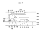
- FIG. 13 to FIG. 17 are process cross-sectional views illustrating a manufacturing method of an organic light emitting diode display according to an exemplary embodiment of the present invention.
- FIG. 1 is a cross-sectional view illustrating an organic light emitting diode display according to an exemplary embodiment of the present invention.
- the organic light emitting diode display may include a substrate 110 , a semiconductor 130 disposed on the substrate 110 , a first gate insulation layer 141 disposed on the semiconductor 130 , a first diffusion barrier layer 151 disposed on the first gate insulation layer 141 , a second diffusion barrier layer 159 in contact with a lateral surface of the first diffusion barrier layer 151 , and a first gate electrode 152 disposed on the first diffusion barrier layer 151 .
- the substrate 110 may include an insulating substrate.
- the insulating substrate may include glass, quartz, ceramic, or plastic.
- exemplary embodiments of the present invention are not limited thereto, and the substrate 110 may include a metal substrate.
- the metal substrate may include stainless steel.
- a buffer layer 120 may be disposed on the substrate 110 .
- the buffer layer 120 may include a silicon nitride (SiN x ) or a silicon oxide (SiO x ).
- the buffer layer 120 may reduce or prevent impurities or moisture from infiltrating the substrate 110 (e.g., while planarizing a surface of the substrate 110 ). According to an exemplary embodiment of the present invention, the buffer layer 120 may be omitted.
- the semiconductor 130 may be disposed on the buffer layer 120 .
- the semiconductor 130 may include an oxide semiconductor material.
- the semiconductor 130 may include a channel region 131 to which an impurity is not doped, and contact doping regions 132 and 133 disposed on opposite sides of the channel region 131 and to which an impurity is doped.
- the contact doping regions 132 and 133 may include a source region 132 and a drain region 133 .
- the impurity may be selected depending on a type of a thin film transistor.
- the first gate insulation layer 141 may include silicon nitride (SiN x ) or silicon oxide (SiO x ).
- the first gate insulation layer 141 may overlap the channel region 131 of the semiconductor 130 .
- the first gate insulation layer 141 need not overlap the source region 132 and the drain region 133 of the semiconductor 130 .
- the first diffusion barrier layer 151 may include a metal.
- the first diffusion barrier layer 151 may include titanium (Ti).
- Ti titanium
- the first diffusion barrier layer 151 may overlap the channel region 131 of the semiconductor 130 .
- the first diffusion barrier layer 151 need not overlap the source region 132 and the drain region 133 of the semiconductor 130 .
- the second diffusion barrier layer 159 may include a metal oxide including the same metal as the first diffusion barrier layer 151 .
- the second diffusion barrier layer 159 may include titanium oxide (TiO x ).
- the second diffusion barrier layer 159 may overlap the source region 132 and the drain region 133 of the semiconductor 130 .
- the second diffusion barrier layer 159 may be disposed directly on the source region 132 and the drain region 133 of the semiconductor 130 .
- the second diffusion barrier layer 159 may cover upper surfaces and lateral surfaces of the source region 132 and the drain region 133 of the semiconductor 130 .
- the second diffusion barrier layer 159 may be substantially entirely overlapped with the source region 132 and the drain region 133 of the semiconductor 130 .
- the second diffusion barrier layer 159 may contact a lateral surface of the first gate insulation layer 141 and may be disposed on the buffer layer 120 .
- the first gate electrode 152 may include copper (Cu).
- the first gate electrode 152 may overlap the channel region 131 of the semiconductor 130 .
- Planar shapes of the first gate electrode 152 and the first diffusion barrier layer 151 may be substantially identical to each other.
- the first gate electrode 152 and the first diffusion barrier layer 151 may have a substantially identical planar shape at a contacting surface between the first gate electrode 152 and the first diffusion barrier layer 151 .
- Lateral surfaces of the first gate electrode 152 and the first diffusion barrier layer 151 may have a tapered shape, and thus, planar shapes of the first gate electrode 152 and the first diffusion barrier layer 151 may be substantially identical to each other.
- planar sizes of the first gate electrode 152 and the first diffusion barrier layer 151 may be slightly different from each other.
- lateral edges of the first gate electrode 152 and the first diffusion barrier layer 151 may be substantially aligned with each other.
- a second gate insulation layer 142 may be disposed on the first gate electrode 152 and the second diffusion barrier layer 159 .
- the second gate insulation layer 142 may include silicon nitride (SiN x ).
- the first gate electrode 152 may include copper (Cu).
- the second gate insulation layer 142 may be formed after the first gate electrode 152 is formed. Since the second gate insulation layer 142 may include silicon nitride (SiN x ), oxidation of copper may be reduced or prevented during a process of forming the second gate insulation layer 142 . Since the first diffusion barrier layer 151 may be disposed under the first gate electrode 152 , a diffusion of hydrogen into the semiconductor 130 during the process of forming the second gate insulation layer 142 may be reduced or prevented.
- the semiconductor 130 may be an oxide semiconductor.
- the second diffusion barrier layer 159 contacting the first diffusion barrier layer 151 may include a metal oxide instead of a metallic material, and edges of the first diffusion barrier layer 151 and the first gate electrode 152 may substantially coincide with each other. Thus, a relatively high current may be prevented from flowing at an edge of the first diffusion barrier layer 151 . Thus, performance of the thin film transistor may be prevented from deteriorating.
- a second gate electrode 154 may be disposed on the second gate insulation layer 142 .
- the second gate electrode 154 may overlap the first gate electrode 152 .
- An interlayer insulation layer 160 may be disposed on the second gate electrode 154 and the second gate insulation layer 142 .
- Contact holes 162 and 164 exposing at least a part of the semiconductor 130 may be formed in the second diffusion barrier layer 159 , the second gate insulation layer 142 , and the interlayer insulation layer 160 .
- the contact holes 162 and 164 may expose the contact doping regions 132 and 133 of the semiconductor 130 .
- a source electrode 173 and a drain electrode 175 may be disposed on the interlayer insulation layer 160 .
- the source electrode 173 may be connected to the source region 132 of the semiconductor 130 through the contact hole 162
- the drain electrode 175 may be connected to the drain region 133 of the semiconductor 130 through the contact hole 164 .
- the semiconductor 130 , the first gate electrode 152 , the source electrode 173 , and the drain electrode 175 may be included in one thin film transistor.
- the thin film transistor may be a switching transistor or a driving transistor.
- the substrate 110 in which the thin film transistor is formed may be referred to as a thin film transistor array panel.
- a passivation layer 180 may be disposed on the interlayer insulation layer 160 , the source electrode 173 , and the drain electrode 175 .
- a contact hole 181 may be formed in the passivation layer 180 to expose at least a part of the drain electrode.
- a pixel electrode 191 may be disposed on the passivation layer 180 .
- the pixel electrode 191 may include a transparent conductive material such as indium-tin oxide (ITO), indium-zinc oxide (IZO), zinc oxide (ZnO), or indium oxide (In 2 O 3 ), or a reflective metal such as lithium (Li), calcium (Ca), lithium fluoride/calcium (LiF/Ca), lithium fluoride/aluminum (LiF/Al), aluminum (Al), silver (Ag), magnesium (Mg), or gold (Au).
- the pixel electrode 191 may be electrically connected to the drain electrode 175 through the contact hole 181 to serve as an anode of an organic light emitting diode (OLED).
- OLED organic light emitting diode
- a pixel definition layer 350 may be disposed on the passivation layer 180 and an edge portion of the pixel electrode 191 .
- the pixel definition layer 350 may include a pixel opening 351 exposing the pixel electrode 191 .
- the pixel definition layer 350 may include a resin such as a polyacrylate, or a polyimide, or a silica-based inorganic material.
- An organic emission layer 370 may be formed in the pixel opening 351 of the pixel definition layer 350 .
- the organic emission layer 370 may include at least one of an emission layer, a hole-injection layer (HIL), a hole-transport layer (HTL), an electron-transport layer (ETL), and an electron-injection layer (EIL).
- HIL hole-injection layer
- HTL hole-transport layer
- ETL electron-transport layer
- EIL electron-injection layer
- the organic emission layer 370 may include a red organic emission layer emitting red light, a green organic emission layer emitting green light, and a blue organic emission layer emitting blue light.
- the red organic emission layer, the green organic emission layer, and the blue organic emission layer may be respectively formed in a red pixel, a green pixel, and a blue pixel to display a color image.
- the organic emission layer 370 may display a color image by stacking a red organic emission layer, a green organic emission layer, and a blue organic emission layer in each of a red pixel, a green pixel, and a blue pixel to form a red filter, a green filter, and a blue filter for each pixel.
- a color image may be displayed by forming a white organic emission layer emitting white light in each of the red pixel, the green pixel, and the blue pixel to form a red filter, a green filter, and a blue filter for each pixel.
- a deposition mask for depositing a red organic emission layer, a green organic emission layer, and a blue organic emission layer on each of the pixels may be omitted.
- the white organic emission layer may include one organic emission layer, or may include a plurality of organic emission layers to emit white light.
- the white organic emission layer may include at least one yellow organic emission layer and at least one blue organic emission layer to emit white light, by combining at least one cyan organic emission layer and at least one red organic emission layer to emit white light, by combining at least one magenta organic emission layer and at least one green organic emission layer to emit white light, and the like.
- a common electrode 270 may be disposed on the pixel definition layer 350 and the organic emission layer 370 .
- the common electrode 270 may include a transparent conductive material such as indium-tin oxide (ITO), indium-zinc oxide (IZO), zinc oxide (ZnO), indium oxide (In 2 O 3 ), or the like, or a reflective metal such as lithium (Li), calcium (Ca), lithium fluoride/calcium (LiF/Ca), lithium fluoride/aluminum (LiF/Al), aluminum (Al), silver (Ag), magnesium (Mg), or gold (Au).
- the common electrode 270 may serve as a cathode of an organic light emitting diode (OLED).
- the pixel electrode 191 , the organic emission layer 370 , and the common electrode 270 may be included in the organic light emitting diode (OLED).
- An organic light emitting diode display may include a first storage electrode 153 disposed on the substrate 110 and a second storage electrode 155 overlapping the first storage electrode 153 .
- the first diffusion barrier layer 151 , the first gate insulation layer 141 , and the buffer layer 120 may be disposed under the first storage electrode 153 .
- the second gate insulation layer 142 may be disposed between the first storage electrode 153 and the second storage electrode 155 .
- the first storage electrode 153 and the second storage electrode 155 may be included in a storage capacitor together with the second gate insulation layer 142 as a dielectric material.
- a manufacturing method of an organic light emitting diode display according to an exemplary embodiment of the present invention will be described in more detail below with reference to FIG. 2 to FIG. 6 .
- FIG. 2 to FIG. 6 are process cross-sectional views illustrating a manufacturing method of an organic light emitting diode display according to an exemplary embodiment of the present invention.
- the buffer layer 120 may be formed by depositing silicon nitride (SiN x ) or silicon oxide (SiO x ) on the substrate 110 .
- the semiconductor 130 may be formed by depositing an oxide semiconductor material on the buffer layer 120 and then patterning it.
- the first gate insulation layer 141 may be formed by depositing silicon nitride (SiN x ) or silicon oxide (SiO x ) on the semiconductor 130 and the buffer layer 120 and then patterning it.
- the semiconductor 130 may include the channel region 131 , and the source region 132 and the drain region 133 disposed on opposite sides of the channel region 131 .
- the first gate insulation layer 141 may overlap the channel region 131 of the semiconductor 130 .
- a first metallic material layer 510 and a second metallic material layer 520 may be sequentially deposited on the first gate insulation layer 141 , the semiconductor 130 , and the buffer layer 120 .
- the first metallic material layer 510 may include titanium (Ti), and the second metallic material layer 520 may include copper (Cu).
- a photoresist pattern 600 may be formed by coating a photosensitive material on the second metallic material layer 520 and then patterning it.
- the first gate electrode 152 and the first storage electrode 153 may be formed by etching the second metallic material layer 520 using the photoresist pattern 600 as a mask.
- the second diffusion barrier layer 159 may be formed by oxidizing the first metallic material layer 510 using the photoresist pattern 600 as a mask. A part of the first metallic material layer 510 , which is disposed under the photoresist pattern 600 , and thus might not be oxidized, may serve as the first diffusion barrier layer 151 .
- the first diffusion barrier layer 151 may include titanium (Ti), and the second diffusion barrier layer 159 may include titanium oxide (TiO x ).
- the photoresist pattern 600 may be employed as a mask to etch the second metallic material layer 520 and to oxidize the first metallic material layer 510 .
- planar shapes of the first gate electrode 152 and the first diffusion barrier layer 151 may be substantially identical to each other. Edges of the first gate electrode 152 and the first diffusion barrier layer 151 may substantially coincide with each other, and the first diffusion barrier layer 151 need not protrude more than the first gate electrode 152 .
- a relatively high current may be reduced or prevented from being generated at an edge of the first diffusion barrier layer 151 , and performance of the thin film transistor may be prevented from deteriorating.
- the photoresist pattern 600 may be removed.
- the second gate insulation layer 142 may be formed by depositing silicon nitride (SiN x ) on the first gate electrode 152 and the second diffusion barrier layer 159 .
- the second gate electrode 154 overlapping the first gate electrode 152 and the second storage electrode 155 formed overlapping the first storage electrode 153 may be formed by depositing a metal material on the second gate insulation layer 142 and then patterning it.
- the interlayer insulation layer 160 may be disposed on the second storage electrode 155 and the second gate insulation layer 142 .
- the contact holes 162 and 164 exposing the source region 132 and the drain region 133 of the semiconductor 130 may be formed by patterning the interlayer insulation layer 160 .
- the source electrode 173 and the drain electrode 175 may be formed by depositing a metal material on the interlayer insulation layer 160 and then patterning it.
- the source electrode 173 and the drain electrode 175 may be respectively connected to the source region 132 and the drain region 133 of the semiconductor 130 through the contact holes 162 and 164 .
- the passivation layer 180 may be disposed on the source electrode 173 , the drain electrode 175 , and the interlayer insulation layer 160 .
- the contact hole 181 exposing the drain electrode 175 may be formed by patterning the passivation layer 180 .
- the pixel electrode 191 may be formed by depositing a metal material on the passivation layer 180 and then patterning it. The pixel electrode 191 may be connected to the drain electrode 175 through the contact hole 181 .
- the pixel definition layer 350 may be formed by depositing an insulating material on the pixel electrode 191 and the passivation layer 180 and then patterning it.
- the pixel definition layer 350 may include the pixel opening 351 formed to expose the pixel electrode 191 .
- the organic emission layer 370 may be formed in the pixel opening 351 .
- the common electrode 270 may be formed by depositing a metal material on the organic emission layer 370 and the pixel definition layer 350 and then patterning it.
- a first gate insulation layer may cover a source region and a drain region as well as a channel region of a semiconductor. The semiconductor will be described in more detail below with reference to FIG. 7 .
- FIG. 7 is a cross-sectional view illustrating the organic light emitting diode display according to an exemplary embodiment of the present invention.
- the organic light emitting diode display may include the substrate 110 , the semiconductor 130 disposed on the substrate 110 , the first gate insulation layer 141 disposed on the semiconductor 130 , the first diffusion barrier layer 151 disposed on the first gate insulation layer 141 , the second diffusion barrier layer 159 in contact with a lateral surface of the first diffusion barrier layer 151 , and the first gate electrode 152 disposed on the first diffusion barrier layer 151 .
- the first gate insulation layer 141 may overlap the channel region 131 of the semiconductor 130 , and might not overlap the source region 132 and the drain region 133 .
- the first gate insulation layer 141 may overlap the channel region 131 , the source region 132 , and the drain region 133 of the semiconductor 130 .
- the first gate insulation layer 141 may be disposed directly on the channel region 131 , the source region 132 , and the drain region 133 of the semiconductor 130 .
- the first gate insulation layer 141 may cover both of an upper surface and a lateral surface of the semiconductor 130 .
- the second diffusion barrier layer 159 may be disposed directly on the source region 132 and the drain region 133 of the semiconductor 130 .
- the first gate insulation layer 141 may be disposed between the second diffusion barrier layer 159 and the source region 132 of the semiconductor 130 and between the second diffusion barrier layer 159 and the drain region 133 of the semiconductor 130 .
- the second diffusion barrier layer 159 may be disposed directly on the first gate insulation layer 141 .
- a manufacturing method of an organic light emitting diode display according to an exemplary embodiment of the present invention will be described in more detail below with reference to FIG. 8 to FIG. 11 .
- the organic light emitting diode display according to an exemplary embodiment of the present invention described with reference to FIG. 8 to FIG. 11 may include substantially identical elements to those of the organic light emitting diode display according to an exemplary embodiment of the present invention described with reference to FIG. 2 to FIG. 6 , duplicative descriptions may be omitted.
- FIG. 8 to FIG. 11 are process cross-sectional views illustrating a manufacturing method of an organic light emitting diode display according to an exemplary embodiment of the present invention.
- the buffer layer 120 may be disposed on the substrate 110 , and the semiconductor 130 may be disposed on the buffer layer 120 .
- the first gate insulation layer 141 , the first metallic material layer 510 , and the second metallic material layer 520 may be sequentially deposited on the semiconductor 130 and the buffer layer 120 .
- the photoresist pattern 600 may be formed by coating a photosensitive material on the second metallic material layer 520 and then patterning it.
- the first gate electrode 152 and the first storage electrode 153 may be formed by etching the second metallic material layer 520 using the photoresist pattern 600 as a mask.
- the second diffusion barrier layer 159 may be formed by oxidizing the first metallic material layer 510 using the photoresist pattern 600 as a mask. A part of the first metallic material layer 510 , which is disposed under the first gate electrode 152 and the first storage electrode 153 and thus might not be oxidized, may serve as the first diffusion barrier layer 151 .
- the first diffusion barrier layer 151 may include titanium (Ti), and the second diffusion barrier layer 159 may include titanium oxide (TiO x ).
- the photoresist pattern 600 may then be removed, and the second gate insulation layer 142 , the second gate electrode 154 , the interlayer insulation layer 160 , the source electrode 173 , the drain electrode 175 , the passivation layer 180 , the pixel electrode 191 , the pixel definition layer 350 , the organic emission layer 370 , and the common electrode 270 may be sequentially formed (see, e.g., FIG. 11 ).
- the organic light emitting diode display according to an exemplary embodiment of the present invention described with reference to FIG. 12 may include substantially identical elements to those of the organic light emitting diode display according to an exemplary embodiment of the present invention described with reference to FIG. 1 , duplicative descriptions may be omitted.
- a source region and a drain region of a semiconductor may be partially rather than entirely overlapped with a second diffusion barrier layer. The semiconductor will be described below in more detail.
- FIG. 12 is a cross-sectional view illustrating an organic light emitting diode display according to an exemplary embodiment of the present invention.
- the organic light emitting diode display may include the substrate 110 , the semiconductor 130 disposed on the substrate 110 , the first gate insulation layer 141 disposed on the semiconductor 130 , the first diffusion barrier layer 151 disposed on the first gate insulation layer 141 , the second diffusion barrier layer 159 contacting a lateral surface of the first diffusion barrier layer 151 , and the first gate electrode 152 disposed on the first diffusion barrier layer 151 .
- the second diffusion barrier layer 159 may cover upper surfaces and lateral surfaces of the source region 132 and the drain region 133 of the semiconductor 130 , and may be substantially entirely overlapped with the source region 132 and the drain region 133 of the semiconductor 130 . According to another exemplary embodiment of the present invention, the second diffusion barrier layer 159 may be partially overlapped with the source region 132 and the drain region 133 of the semiconductor 130 . Most of the source region 132 and the drain region 133 of the semiconductor 130 might not be covered with the second diffusion barrier layer 159 .
- the second gate insulation layer 142 may be disposed on the first gate electrode 152 , the second diffusion barrier layer 159 , and the semiconductor 130 .
- the second gate insulation layer 142 may be disposed directly on the source region 132 and the drain region 133 of the semiconductor 130 .
- a manufacturing method of an organic light emitting diode display according to an exemplary embodiment of the present invention will be described in more detail below with reference to FIG. 13 to FIG. 17 .
- the organic light emitting diode display according to an exemplary embodiment of the present invention described with reference to FIG. 13 to FIG. 17 may include substantially identical elements to those of the organic light emitting diode display according to an exemplary embodiment of the present invention described with reference to FIG. 2 to FIG. 6 , duplicative descriptions may be omitted.
- FIG. 13 to FIG. 17 are process cross-sectional views illustrating a manufacturing method of an organic light emitting diode display according to an exemplary embodiment of the present invention.
- the buffer layer 120 may be disposed on the substrate 110 , and the semiconductor 130 may be disposed on the buffer layer 120 .
- the first gate insulation layer 141 , the first metallic material layer 510 , and the second metallic material layer 520 may be sequentially deposited on the semiconductor 130 and the buffer layer 120 .
- the photoresist pattern 600 may be formed by coating a photosensitive material on the second metallic material layer 520 and then patterning it.
- the first gate electrode 152 and the first storage electrode 153 may be formed by jointly etching the second metallic material layer 520 and the first metallic material layer 510 using the photoresist pattern 600 as a mask.
- the second metallic material layer 520 and the first metallic material layer 510 may be jointly etched by a wet etching method.
- a part of the first metallic material layer 510 may be protruded more than the first gate electrode 152 because of a difference between an etching rate of the first metallic material layer 510 and an etching rate of the second metallic material layer 520 .
- the first gate insulation layer 141 is etched by using the photoresist pattern 600 as a mask.
- the first gate insulation layer 141 may be etched by a dry etching method.
- the second diffusion barrier layer 159 may be formed by oxidizing the first metallic material layer 510 using the photoresist pattern 600 as a mask. A part of the first metallic material layer 510 which is disposed under the first gate electrode 152 and the first storage electrode 153 and thus might not be oxidized may serve as the first diffusion barrier layer 151 .
- the first diffusion barrier layer 151 may include titanium (Ti), and the second diffusion barrier layer 159 may include titanium oxide (TiO x ).
- the photoresist pattern 600 may be removed, and the second gate insulation layer 142 , the second gate electrode 154 , the interlayer insulation layer 160 , the source electrode 173 , the drain electrode 175 , the passivation layer 180 , the pixel electrode 191 , the pixel definition layer 350 , the organic emission layer 370 , and the common electrode 270 may be sequentially formed (see, e.g., FIG. 17 ).
Priority Applications (1)
| Application Number | Priority Date | Filing Date | Title |
|---|---|---|---|
| US16/250,642 US10734461B2 (en) | 2015-12-02 | 2019-01-17 | Thin film transistor array panel and organic light emitting diode display including the same |
Applications Claiming Priority (2)
| Application Number | Priority Date | Filing Date | Title |
|---|---|---|---|
| KR10-2015-0170781 | 2015-12-02 | ||
| KR1020150170781A KR102517127B1 (ko) | 2015-12-02 | 2015-12-02 | 박막 트랜지스터 표시판 및 이를 포함하는 유기 발광 표시 장치 |
Related Child Applications (1)
| Application Number | Title | Priority Date | Filing Date |
|---|---|---|---|
| US16/250,642 Continuation US10734461B2 (en) | 2015-12-02 | 2019-01-17 | Thin film transistor array panel and organic light emitting diode display including the same |
Publications (2)
| Publication Number | Publication Date |
|---|---|
| US20170162640A1 US20170162640A1 (en) | 2017-06-08 |
| US10192944B2 true US10192944B2 (en) | 2019-01-29 |
Family
ID=58798593
Family Applications (2)
| Application Number | Title | Priority Date | Filing Date |
|---|---|---|---|
| US15/237,866 Active US10192944B2 (en) | 2015-12-02 | 2016-08-16 | Thin film transistor array panel with diffusion barrier layer and gate insulation layer and organic light emitting diode display including the same |
| US16/250,642 Active US10734461B2 (en) | 2015-12-02 | 2019-01-17 | Thin film transistor array panel and organic light emitting diode display including the same |
Family Applications After (1)
| Application Number | Title | Priority Date | Filing Date |
|---|---|---|---|
| US16/250,642 Active US10734461B2 (en) | 2015-12-02 | 2019-01-17 | Thin film transistor array panel and organic light emitting diode display including the same |
Country Status (2)
| Country | Link |
|---|---|
| US (2) | US10192944B2 (ko) |
| KR (1) | KR102517127B1 (ko) |
Families Citing this family (8)
| Publication number | Priority date | Publication date | Assignee | Title |
|---|---|---|---|---|
| JP2017034060A (ja) * | 2015-07-31 | 2017-02-09 | 株式会社ジャパンディスプレイ | 半導体装置及び表示装置 |
| KR102490895B1 (ko) * | 2017-12-14 | 2023-01-25 | 삼성디스플레이 주식회사 | 디스플레이 장치 및 그 제조방법 |
| KR102630641B1 (ko) | 2018-01-25 | 2024-01-30 | 삼성디스플레이 주식회사 | 표시장치 및 그의 제조방법 |
| KR102548987B1 (ko) | 2018-08-09 | 2023-06-29 | 삼성디스플레이 주식회사 | 디스플레이 장치 |
| CN110197831B (zh) * | 2019-06-19 | 2021-09-10 | 京东方科技集团股份有限公司 | 一种阵列基板及其制作方法和显示面板 |
| KR20210004795A (ko) * | 2019-07-04 | 2021-01-13 | 엘지디스플레이 주식회사 | 디스플레이 장치 |
| CN112186004A (zh) * | 2019-07-04 | 2021-01-05 | 乐金显示有限公司 | 显示设备 |
| CN111710726B (zh) * | 2020-06-12 | 2021-10-08 | 深圳市华星光电半导体显示技术有限公司 | 薄膜晶体管基板及薄膜晶体管基板的制备方法 |
Citations (7)
| Publication number | Priority date | Publication date | Assignee | Title |
|---|---|---|---|---|
| KR20100059586A (ko) | 2008-11-26 | 2010-06-04 | 엘지디스플레이 주식회사 | 산화물 박막 트랜지스터 및 그 제조방법 |
| US20110084272A1 (en) | 2009-10-09 | 2011-04-14 | Semiconductor Energy Laboratory Co., Ltd. | Semiconductor device and method for manufacturing the same |
| KR20130094161A (ko) | 2012-02-15 | 2013-08-23 | 엘지디스플레이 주식회사 | 박막트랜지스터, 박막트랜지스터 어레이 기판 및 이의 제조방법 |
| KR20130129674A (ko) | 2012-05-21 | 2013-11-29 | 삼성디스플레이 주식회사 | 박막 트랜지스터 및 이를 포함하는 박막 트랜지스터 표시판 |
| US20130320317A1 (en) * | 2012-06-05 | 2013-12-05 | Innolux Corporation | Thin film transistor substrate and display |
| US20140048800A1 (en) * | 2009-11-30 | 2014-02-20 | Samsung Display Co., Ltd. | Thin film transistor having oxide semiconductor layer as ohmic contact layer |
| KR101479917B1 (ko) | 2009-02-20 | 2015-01-07 | 가부시키가이샤 한도오따이 에네루기 켄큐쇼 | 박막 트랜지스터 및 그 제작 방법, 및 반도체 장치 |
Family Cites Families (9)
| Publication number | Priority date | Publication date | Assignee | Title |
|---|---|---|---|---|
| JP4955848B2 (ja) * | 2000-02-28 | 2012-06-20 | エルジー ディスプレイ カンパニー リミテッド | 電子素子用基板製造方法 |
| JP4434644B2 (ja) * | 2003-07-18 | 2010-03-17 | 東芝モバイルディスプレイ株式会社 | 薄膜トランジスタの製造方法と、この薄膜トランジスタを備える表示装置の製造方法 |
| KR100873081B1 (ko) * | 2007-05-29 | 2008-12-09 | 삼성모바일디스플레이주식회사 | 박막 트랜지스터, 그의 제조 방법 및 박막 트랜지스터를구비하는 평판 표시 장치 |
| JP2011159908A (ja) * | 2010-02-03 | 2011-08-18 | Sony Corp | 薄膜トランジスタおよびその製造方法、並びに表示装置 |
| JP2012039019A (ja) * | 2010-08-11 | 2012-02-23 | Renesas Electronics Corp | 半導体装置およびその製造方法 |
| CN106920907B (zh) | 2011-04-28 | 2021-01-15 | 佐尔循环公司 | 用于将电池组保持在电池室内的闩锁组件 |
| US9653614B2 (en) * | 2012-01-23 | 2017-05-16 | Semiconductor Energy Laboratory Co., Ltd. | Semiconductor device and method for manufacturing the same |
| KR101486038B1 (ko) * | 2012-08-02 | 2015-01-26 | 삼성디스플레이 주식회사 | 유기 발광 표시 장치 |
| JP6111458B2 (ja) * | 2013-03-28 | 2017-04-12 | 株式会社Joled | 半導体装置、表示装置および電子機器 |
-
2015
- 2015-12-02 KR KR1020150170781A patent/KR102517127B1/ko active IP Right Grant
-
2016
- 2016-08-16 US US15/237,866 patent/US10192944B2/en active Active
-
2019
- 2019-01-17 US US16/250,642 patent/US10734461B2/en active Active
Patent Citations (8)
| Publication number | Priority date | Publication date | Assignee | Title |
|---|---|---|---|---|
| KR20100059586A (ko) | 2008-11-26 | 2010-06-04 | 엘지디스플레이 주식회사 | 산화물 박막 트랜지스터 및 그 제조방법 |
| KR101479917B1 (ko) | 2009-02-20 | 2015-01-07 | 가부시키가이샤 한도오따이 에네루기 켄큐쇼 | 박막 트랜지스터 및 그 제작 방법, 및 반도체 장치 |
| US20110084272A1 (en) | 2009-10-09 | 2011-04-14 | Semiconductor Energy Laboratory Co., Ltd. | Semiconductor device and method for manufacturing the same |
| KR20120084760A (ko) | 2009-10-09 | 2012-07-30 | 가부시키가이샤 한도오따이 에네루기 켄큐쇼 | 반도체 장치 및 이를 제조하기 위한 방법 |
| US20140048800A1 (en) * | 2009-11-30 | 2014-02-20 | Samsung Display Co., Ltd. | Thin film transistor having oxide semiconductor layer as ohmic contact layer |
| KR20130094161A (ko) | 2012-02-15 | 2013-08-23 | 엘지디스플레이 주식회사 | 박막트랜지스터, 박막트랜지스터 어레이 기판 및 이의 제조방법 |
| KR20130129674A (ko) | 2012-05-21 | 2013-11-29 | 삼성디스플레이 주식회사 | 박막 트랜지스터 및 이를 포함하는 박막 트랜지스터 표시판 |
| US20130320317A1 (en) * | 2012-06-05 | 2013-12-05 | Innolux Corporation | Thin film transistor substrate and display |
Also Published As
| Publication number | Publication date |
|---|---|
| US10734461B2 (en) | 2020-08-04 |
| US20170162640A1 (en) | 2017-06-08 |
| KR102517127B1 (ko) | 2023-04-03 |
| KR20170065069A (ko) | 2017-06-13 |
| US20190157367A1 (en) | 2019-05-23 |
Similar Documents
| Publication | Publication Date | Title |
|---|---|---|
| US10734461B2 (en) | Thin film transistor array panel and organic light emitting diode display including the same | |
| US10840481B2 (en) | Organic light-emitting display apparatus and method of manufacturing the same | |
| US20220123262A1 (en) | Organic light-emitting display apparatus and method of manufacturing the same | |
| KR101084177B1 (ko) | 유기 발광 디스플레이 장치 및 그의 제조 방법 | |
| US8203264B2 (en) | Flat panel display and method of fabricating the same | |
| US8981362B2 (en) | Organic light-emitting display device and method of manufacturing the same | |
| US8455893B2 (en) | Light-emitting apparatus and production method thereof | |
| US10347705B2 (en) | Organic light emitting diode display and manufacturing method thereof | |
| CN104051493A (zh) | 有机发光显示装置 | |
| US10672844B2 (en) | Organic light emitting diode display | |
| KR102539076B1 (ko) | 표시 장치 | |
| US10032849B2 (en) | Organic light emitting diode display device and manufacturing method thereof | |
| US9640761B2 (en) | Organic light-emitting diode display and method of manufacturing the same | |
| KR20150027434A (ko) | 유기 발광 표시 장치 및 그 제조 방법 | |
| KR20170080996A (ko) | 표시 장치용 박막 트랜지스터 및 이를 포함하는 유기 발광 표시 장치 | |
| US9245905B2 (en) | Back plane for flat panel display device and method of manufacturing the same | |
| JP5063294B2 (ja) | 発光装置及びその製造方法 | |
| KR101899477B1 (ko) | 박막 트랜지스터, 그 제조방법 및 이를 포함하는 유기 발광 표시장치 | |
| US20150270323A1 (en) | Organic light-emitting display apparatus and manufacturing method thereof | |
| US9806275B2 (en) | Organic light emitting diode display | |
| KR20220143252A (ko) | 유기발광 표시장치 및 제조방법 | |
| US20150200238A1 (en) | Thin film transistor, method of manufacturing the thin film transistor and flat panel display device having the thin film transistor | |
| KR20180012686A (ko) | 표시 장치 |
Legal Events
| Date | Code | Title | Description |
|---|---|---|---|
| AS | Assignment |
Owner name: SAMSUNG DISPLAY CO., LTD., KOREA, REPUBLIC OF Free format text: ASSIGNMENT OF ASSIGNORS INTEREST;ASSIGNORS:LEE, DONG HEE;KANG, HYUN JU;SHIN, SANG WON;REEL/FRAME:039453/0413 Effective date: 20160427 |
|
| STCF | Information on status: patent grant |
Free format text: PATENTED CASE |
|
| MAFP | Maintenance fee payment |
Free format text: PAYMENT OF MAINTENANCE FEE, 4TH YEAR, LARGE ENTITY (ORIGINAL EVENT CODE: M1551); ENTITY STATUS OF PATENT OWNER: LARGE ENTITY Year of fee payment: 4 |