JP5063294B2 - 発光装置及びその製造方法 - Google Patents
発光装置及びその製造方法 Download PDFInfo
- Publication number
- JP5063294B2 JP5063294B2 JP2007280166A JP2007280166A JP5063294B2 JP 5063294 B2 JP5063294 B2 JP 5063294B2 JP 2007280166 A JP2007280166 A JP 2007280166A JP 2007280166 A JP2007280166 A JP 2007280166A JP 5063294 B2 JP5063294 B2 JP 5063294B2
- Authority
- JP
- Japan
- Prior art keywords
- electrode
- light emitting
- layer
- light
- conductive layer
- Prior art date
- Legal status (The legal status is an assumption and is not a legal conclusion. Google has not performed a legal analysis and makes no representation as to the accuracy of the status listed.)
- Active
Links
- 238000004519 manufacturing process Methods 0.000 title claims description 24
- 238000002955 isolation Methods 0.000 claims description 41
- XLOMVQKBTHCTTD-UHFFFAOYSA-N Zinc monoxide Chemical compound [Zn]=O XLOMVQKBTHCTTD-UHFFFAOYSA-N 0.000 claims description 32
- 239000000758 substrate Substances 0.000 claims description 30
- 239000000956 alloy Substances 0.000 claims description 17
- 229910045601 alloy Inorganic materials 0.000 claims description 17
- 229910052782 aluminium Inorganic materials 0.000 claims description 17
- XAGFODPZIPBFFR-UHFFFAOYSA-N aluminium Chemical compound [Al] XAGFODPZIPBFFR-UHFFFAOYSA-N 0.000 claims description 17
- 239000011787 zinc oxide Substances 0.000 claims description 16
- 150000001875 compounds Chemical class 0.000 claims description 12
- RTAQQCXQSZGOHL-UHFFFAOYSA-N Titanium Chemical compound [Ti] RTAQQCXQSZGOHL-UHFFFAOYSA-N 0.000 claims description 11
- 238000000034 method Methods 0.000 claims description 11
- 239000010936 titanium Substances 0.000 claims description 11
- 229910052719 titanium Inorganic materials 0.000 claims description 11
- AMGQUBHHOARCQH-UHFFFAOYSA-N indium;oxotin Chemical compound [In].[Sn]=O AMGQUBHHOARCQH-UHFFFAOYSA-N 0.000 claims description 9
- GYHNNYVSQQEPJS-UHFFFAOYSA-N Gallium Chemical compound [Ga] GYHNNYVSQQEPJS-UHFFFAOYSA-N 0.000 claims description 8
- XUIMIQQOPSSXEZ-UHFFFAOYSA-N Silicon Chemical compound [Si] XUIMIQQOPSSXEZ-UHFFFAOYSA-N 0.000 claims description 8
- 229910052733 gallium Inorganic materials 0.000 claims description 8
- 229910052710 silicon Inorganic materials 0.000 claims description 8
- 239000010703 silicon Substances 0.000 claims description 8
- RYGMFSIKBFXOCR-UHFFFAOYSA-N Copper Chemical compound [Cu] RYGMFSIKBFXOCR-UHFFFAOYSA-N 0.000 claims description 6
- 229910052802 copper Inorganic materials 0.000 claims description 6
- 239000010949 copper Substances 0.000 claims description 6
- 229910052758 niobium Inorganic materials 0.000 claims description 6
- 239000010955 niobium Substances 0.000 claims description 6
- GUCVJGMIXFAOAE-UHFFFAOYSA-N niobium atom Chemical compound [Nb] GUCVJGMIXFAOAE-UHFFFAOYSA-N 0.000 claims description 6
- 229910052706 scandium Inorganic materials 0.000 claims description 6
- SIXSYDAISGFNSX-UHFFFAOYSA-N scandium atom Chemical compound [Sc] SIXSYDAISGFNSX-UHFFFAOYSA-N 0.000 claims description 6
- ZOKXTWBITQBERF-UHFFFAOYSA-N Molybdenum Chemical compound [Mo] ZOKXTWBITQBERF-UHFFFAOYSA-N 0.000 claims description 5
- NRTOMJZYCJJWKI-UHFFFAOYSA-N Titanium nitride Chemical compound [Ti]#N NRTOMJZYCJJWKI-UHFFFAOYSA-N 0.000 claims description 5
- 229910052750 molybdenum Inorganic materials 0.000 claims description 5
- 239000011733 molybdenum Substances 0.000 claims description 5
- 229910052715 tantalum Inorganic materials 0.000 claims description 5
- GUVRBAGPIYLISA-UHFFFAOYSA-N tantalum atom Chemical compound [Ta] GUVRBAGPIYLISA-UHFFFAOYSA-N 0.000 claims description 5
- WFKWXMTUELFFGS-UHFFFAOYSA-N tungsten Chemical compound [W] WFKWXMTUELFFGS-UHFFFAOYSA-N 0.000 claims description 5
- 229910052721 tungsten Inorganic materials 0.000 claims description 5
- 239000010937 tungsten Substances 0.000 claims description 5
- 239000002131 composite material Substances 0.000 claims description 4
- 238000005192 partition Methods 0.000 claims description 4
- 239000000126 substance Substances 0.000 claims description 2
- 238000007740 vapor deposition Methods 0.000 claims description 2
- 238000010030 laminating Methods 0.000 claims 1
- 208000024891 symptom Diseases 0.000 claims 1
- 239000010410 layer Substances 0.000 description 116
- 239000010408 film Substances 0.000 description 24
- 238000010586 diagram Methods 0.000 description 9
- 239000000463 material Substances 0.000 description 9
- 239000012044 organic layer Substances 0.000 description 9
- 239000011521 glass Substances 0.000 description 7
- 238000005530 etching Methods 0.000 description 5
- 239000011159 matrix material Substances 0.000 description 4
- 239000007769 metal material Substances 0.000 description 4
- 238000003825 pressing Methods 0.000 description 4
- 230000015572 biosynthetic process Effects 0.000 description 3
- 239000004020 conductor Substances 0.000 description 3
- 230000005525 hole transport Effects 0.000 description 3
- 238000000059 patterning Methods 0.000 description 3
- 230000000737 periodic effect Effects 0.000 description 3
- 238000007789 sealing Methods 0.000 description 3
- 229910052709 silver Inorganic materials 0.000 description 3
- 239000004332 silver Substances 0.000 description 3
- 229910052779 Neodymium Inorganic materials 0.000 description 2
- 229910052581 Si3N4 Inorganic materials 0.000 description 2
- 229910004298 SiO 2 Inorganic materials 0.000 description 2
- VYPSYNLAJGMNEJ-UHFFFAOYSA-N Silicium dioxide Chemical compound O=[Si]=O VYPSYNLAJGMNEJ-UHFFFAOYSA-N 0.000 description 2
- BQCADISMDOOEFD-UHFFFAOYSA-N Silver Chemical compound [Ag] BQCADISMDOOEFD-UHFFFAOYSA-N 0.000 description 2
- 239000003086 colorant Substances 0.000 description 2
- 238000000151 deposition Methods 0.000 description 2
- 239000011229 interlayer Substances 0.000 description 2
- 238000001459 lithography Methods 0.000 description 2
- QEFYFXOXNSNQGX-UHFFFAOYSA-N neodymium atom Chemical compound [Nd] QEFYFXOXNSNQGX-UHFFFAOYSA-N 0.000 description 2
- 229910021420 polycrystalline silicon Inorganic materials 0.000 description 2
- 229920001721 polyimide Polymers 0.000 description 2
- 238000000926 separation method Methods 0.000 description 2
- HQVNEWCFYHHQES-UHFFFAOYSA-N silicon nitride Chemical compound N12[Si]34N5[Si]62N3[Si]51N64 HQVNEWCFYHHQES-UHFFFAOYSA-N 0.000 description 2
- 229910052814 silicon oxide Inorganic materials 0.000 description 2
- 238000004544 sputter deposition Methods 0.000 description 2
- IATRAKWUXMZMIY-UHFFFAOYSA-N strontium oxide Chemical compound [O-2].[Sr+2] IATRAKWUXMZMIY-UHFFFAOYSA-N 0.000 description 2
- GOLORTLGFDVFDW-UHFFFAOYSA-N 3-(1h-benzimidazol-2-yl)-7-(diethylamino)chromen-2-one Chemical compound C1=CC=C2NC(C3=CC4=CC=C(C=C4OC3=O)N(CC)CC)=NC2=C1 GOLORTLGFDVFDW-UHFFFAOYSA-N 0.000 description 1
- 239000004925 Acrylic resin Substances 0.000 description 1
- 229920000178 Acrylic resin Polymers 0.000 description 1
- 239000004642 Polyimide Substances 0.000 description 1
- 229910007541 Zn O Inorganic materials 0.000 description 1
- 238000010521 absorption reaction Methods 0.000 description 1
- BRPQOXSCLDDYGP-UHFFFAOYSA-N calcium oxide Chemical compound [O-2].[Ca+2] BRPQOXSCLDDYGP-UHFFFAOYSA-N 0.000 description 1
- ODINCKMPIJJUCX-UHFFFAOYSA-N calcium oxide Inorganic materials [Ca]=O ODINCKMPIJJUCX-UHFFFAOYSA-N 0.000 description 1
- 239000000292 calcium oxide Substances 0.000 description 1
- 239000000470 constituent Substances 0.000 description 1
- 230000008021 deposition Effects 0.000 description 1
- 230000006866 deterioration Effects 0.000 description 1
- 238000009826 distribution Methods 0.000 description 1
- 230000000694 effects Effects 0.000 description 1
- 238000005401 electroluminescence Methods 0.000 description 1
- 239000003822 epoxy resin Substances 0.000 description 1
- 230000001747 exhibiting effect Effects 0.000 description 1
- 238000000605 extraction Methods 0.000 description 1
- 238000003384 imaging method Methods 0.000 description 1
- CECAIMUJVYQLKA-UHFFFAOYSA-N iridium 1-phenylisoquinoline Chemical compound [Ir].C1=CC=CC=C1C1=NC=CC2=CC=CC=C12.C1=CC=CC=C1C1=NC=CC2=CC=CC=C12.C1=CC=CC=C1C1=NC=CC2=CC=CC=C12 CECAIMUJVYQLKA-UHFFFAOYSA-N 0.000 description 1
- 229910052751 metal Inorganic materials 0.000 description 1
- 239000002184 metal Substances 0.000 description 1
- 239000012299 nitrogen atmosphere Substances 0.000 description 1
- 229920003986 novolac Polymers 0.000 description 1
- 239000011368 organic material Substances 0.000 description 1
- 230000002093 peripheral effect Effects 0.000 description 1
- 125000002080 perylenyl group Chemical group C1(=CC=C2C=CC=C3C4=CC=CC5=CC=CC(C1=C23)=C45)* 0.000 description 1
- CSHWQDPOILHKBI-UHFFFAOYSA-N peryrene Natural products C1=CC(C2=CC=CC=3C2=C2C=CC=3)=C3C2=CC=CC3=C1 CSHWQDPOILHKBI-UHFFFAOYSA-N 0.000 description 1
- 229920002120 photoresistant polymer Polymers 0.000 description 1
- 229920000647 polyepoxide Polymers 0.000 description 1
- 239000009719 polyimide resin Substances 0.000 description 1
- 230000001681 protective effect Effects 0.000 description 1
- 238000009751 slip forming Methods 0.000 description 1
- 238000000638 solvent extraction Methods 0.000 description 1
- 238000004528 spin coating Methods 0.000 description 1
- 239000010409 thin film Substances 0.000 description 1
- 238000002834 transmittance Methods 0.000 description 1
- TVIVIEFSHFOWTE-UHFFFAOYSA-K tri(quinolin-8-yloxy)alumane Chemical compound [Al+3].C1=CN=C2C([O-])=CC=CC2=C1.C1=CN=C2C([O-])=CC=CC2=C1.C1=CN=C2C([O-])=CC=CC2=C1 TVIVIEFSHFOWTE-UHFFFAOYSA-K 0.000 description 1
Images


Description
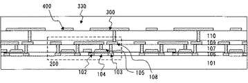
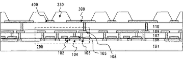
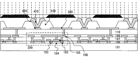
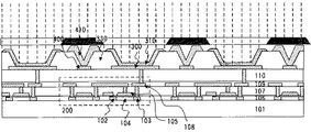
基板の上に第1電極と発光媒体と第2電極とを順に有する複数の発光素子と、
前記複数の発光素子の間に形成されて各発光素子を区画する素子分離層と、
前記基板と前記素子分離層との間に形成されて前記第2電極と電気的に接続される補助電極と、を有する発光装置の製造方法であって、
基板の上に、第1電極と、補助電極とを形成する工程と、
前記第1電極を露出する開口と前記補助電極を露出する開口とを有する素子分離層を形成する工程と、
前記素子分離層と前記補助電極を露出する開口とを覆う導電層を形成する工程と、
前記導電層にシャドウマスクを当接させて、前記第1電極を露出する開口に、前記導電層よりも厚みの薄い発光媒体を形成する工程と、
前記発光媒体と、前記素子分離層と、前記導電層とを覆う第2電極を形成する工程と、を有することを特徴とする。
前記複数の発光素子の間に形成されて各発光素子を区画する素子分離層と、
前記基板と前記素子分離層との間に形成されて前記第2電極と電気的に接続される補助電極と、を有する発光装置であって、
前記素子分離層は前記補助電極を露出する開口を有し、
前記素子分離層と、前記補助電極を露出する開口とには導電層が配置され、
前記導電層を介して前記第2電極と前記補助電極とが電気的に接続されており、
前記導電層の厚みは、前記発光媒体の厚みよりも厚いことを特徴とする。
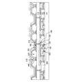
102 ソース領域
103 ドレイン領域
104 Poly−Si
105 ゲート電極
106 ゲート絶縁膜
107 層間絶縁膜
108 ドレイン電極
109 無機絶縁膜
110 平坦化層
200 TFT
300 第1電極
310 発光媒体
311 正孔輸送層
312 発光層
313 電子輸送層
320 第2電極
330 素子分離層
400 補助電極
410 導電層
Claims (9)
- 基板の上に第1電極と発光媒体と第2電極とを順に有する複数の発光素子と、
前記複数の発光素子の間に形成されて各発光素子を区画する素子分離層と、
前記基板と前記素子分離層との間に形成されて前記第2電極と電気的に接続される補助電極と、を有する発光装置の製造方法であって、
基板の上に、第1電極と、補助電極とを形成する工程と、
前記第1電極を露出する開口と前記補助電極を露出する開口とを有する素子分離層を形成する工程と、
前記素子分離層と前記補助電極を露出する開口とを覆う導電層を形成する工程と、
前記導電層にシャドウマスクを当接させて、前記第1電極を露出する開口に、前記導電層よりも厚みの薄い発光媒体を形成する工程と、
前記発光媒体と、前記素子分離層と、前記導電層とを覆う第2電極を形成する工程と、を有することを特徴とする発光装置の製造方法。 - 前記発光媒体を形成する工程は、マスク開口パターンの異なる複数のシャドウマスクを用いて、複数の層を形成する工程を有することを特徴とする請求項1に記載の発光装置の製造方法。
- 前記導電層を形成する工程は、マスクを用いた蒸着法によって形成する工程であることを特徴とする請求項1または請求項2に記載の発光装置の製造方法。
- 前記発光媒体を形成する工程において、前記シャドウマスクは、前記素子分離層の前記補助電極を露出する開口に倣って形成された前記導電層の窪みを覆っていることを特徴とする請求項1乃至請求項3のいずれか一項に記載の発光装置の製造方法。
- 前記補助電極を、アルミニウム、アルミニウムとチタン、スカンジウム、ニオブ、銅若しくはシリコンとの合金、又はチタン、窒化チタン、タンタル、タングステン若しくはモリブデンの単体若しくはこれらの合金若しくは積層膜で形成した反射性電極上に酸化インジウム・スズ、酸化亜鉛、ガリウムが添加された酸化亜鉛、若しくはこれらの化合物を積層した複合層として形成し、前記導電層を、アルミニウム、アルミニウムとチタン、スカンジウム、ニオブ、銅若しくはシリコンとの合金、又はチタン、窒化チタン、タンタル、タングステン若しくはモリブデンの単体若しくはこれらの合金若しくは積層膜で形成し、前記第2電極を、酸化インジウム・スズ、酸化亜鉛、ガリウムが添加された酸化亜鉛又はこれらの化合物で形成することを特徴とする請求項1乃至請求項4のいずれか一項に記載の発光装置の製造方法。
- 基板の上に第1電極と発光媒体と第2電極とを順に有する複数の発光素子と、
前記複数の発光素子の間に形成されて各発光素子を区画する素子分離層と、
前記基板と前記素子分離層との間に形成されて前記第2電極と電気的に接続される補助電極と、を有する発光装置であって、
前記素子分離層は前記補助電極を露出する開口を有し、
前記素子分離層と、前記補助電極を露出する開口とには導電層が配置され、
前記導電層を介して前記第2電極と前記補助電極とが電気的に接続されており、
前記導電層の厚みは、前記発光媒体の厚みよりも厚いことを特徴とする発光装置。 - 前記導電層は、互いに離間して形成されている複数のドット状の部材であることを特徴とする請求項6に記載の発光装置。
- 前記補助電極は、前記第1電極と同一の平面に形成された層であることを特徴とする請求項6または請求項7に記載の発光装置。
- 前記補助電極は、アルミニウム、アルミニウムとチタン、スカンジウム、ニオブ、銅若しくはシリコンとの合金、又はチタン、窒化チタン、タンタル、タングステン若しくはモリブデンの単体若しくはこれらの合金若しくは積層膜で形成された反射性電極上に酸化インジウム・スズ、酸化亜鉛、ガリウムが添加された酸化亜鉛、若しくはこれらの化合物を積層した複合層であり、前記導電層は、アルミニウム、アルミニウムとチタン、スカンジウム、ニオブ、銅若しくはシリコンとの合金、又はチタン、窒化チタン、タンタル、タングステン若しくはモリブデンの単体若しくはこれらの合金若しくは積層膜で形成され前記第2電極は、酸化インジウム・スズ、酸化亜鉛、ガリウムが添加された酸化亜鉛又はこれらの化合物で形成されることを特徴とする請求項6乃至請求項8のいずれか一項に記載の発光装置。
Priority Applications (3)
| Application Number | Priority Date | Filing Date | Title |
|---|---|---|---|
| JP2007280166A JP5063294B2 (ja) | 2006-11-17 | 2007-10-29 | 発光装置及びその製造方法 |
| US11/939,733 US7985609B2 (en) | 2006-11-17 | 2007-11-14 | Light-emitting apparatus and production method thereof |
| US13/163,971 US8455893B2 (en) | 2006-11-17 | 2011-06-20 | Light-emitting apparatus and production method thereof |
Applications Claiming Priority (3)
| Application Number | Priority Date | Filing Date | Title |
|---|---|---|---|
| JP2006311252 | 2006-11-17 | ||
| JP2006311252 | 2006-11-17 | ||
| JP2007280166A JP5063294B2 (ja) | 2006-11-17 | 2007-10-29 | 発光装置及びその製造方法 |
Publications (3)
| Publication Number | Publication Date |
|---|---|
| JP2008146026A JP2008146026A (ja) | 2008-06-26 |
| JP2008146026A5 JP2008146026A5 (ja) | 2010-12-16 |
| JP5063294B2 true JP5063294B2 (ja) | 2012-10-31 |
Family
ID=39606231
Family Applications (1)
| Application Number | Title | Priority Date | Filing Date |
|---|---|---|---|
| JP2007280166A Active JP5063294B2 (ja) | 2006-11-17 | 2007-10-29 | 発光装置及びその製造方法 |
Country Status (1)
| Country | Link |
|---|---|
| JP (1) | JP5063294B2 (ja) |
Families Citing this family (7)
| Publication number | Priority date | Publication date | Assignee | Title |
|---|---|---|---|---|
| KR20100007266A (ko) * | 2008-07-11 | 2010-01-22 | 삼성모바일디스플레이주식회사 | 유기 발광 표시 장치 및 그 제조 방법 |
| JP2010062003A (ja) * | 2008-09-04 | 2010-03-18 | Hitachi Displays Ltd | 表示装置 |
| CN102172101B (zh) * | 2008-10-06 | 2015-07-08 | 旭硝子株式会社 | 电子器件用基板及其制造方法、使用该基板的电子器件及其制造方法以及有机led元件用基板 |
| JP2014029814A (ja) * | 2012-07-31 | 2014-02-13 | Sony Corp | 表示装置および電子機器 |
| KR102155815B1 (ko) * | 2014-08-05 | 2020-09-14 | 엘지디스플레이 주식회사 | 유기 발광 표시 장치 및 이의 제조 방법 |
| WO2018225183A1 (ja) * | 2017-06-07 | 2018-12-13 | シャープ株式会社 | 表示デバイス、表示デバイスの製造方法、表示デバイスの製造装置 |
| TW202232752A (zh) * | 2020-12-24 | 2022-08-16 | 日商半導體能源研究所股份有限公司 | 顯示裝置 |
Family Cites Families (6)
| Publication number | Priority date | Publication date | Assignee | Title |
|---|---|---|---|---|
| JP3077688B1 (ja) * | 1999-02-12 | 2000-08-14 | 日本電気株式会社 | 有機薄膜elパネルとその製造方法 |
| JP2002151255A (ja) * | 2000-11-10 | 2002-05-24 | Sharp Corp | 有機エレクトロルミネッセンスディスプレイパネル及びその製造方法 |
| JP2002318556A (ja) * | 2001-04-20 | 2002-10-31 | Toshiba Corp | アクティブマトリクス型平面表示装置およびその製造方法 |
| JP2004031262A (ja) * | 2002-06-28 | 2004-01-29 | Matsushita Electric Ind Co Ltd | 有機エレクトロルミネッセンスパネル |
| JP2005322564A (ja) * | 2004-05-11 | 2005-11-17 | Sony Corp | 表示装置の製造方法および表示装置 |
| JP4725054B2 (ja) * | 2004-08-24 | 2011-07-13 | ソニー株式会社 | 表示装置 |
-
2007
- 2007-10-29 JP JP2007280166A patent/JP5063294B2/ja active Active
Also Published As
| Publication number | Publication date |
|---|---|
| JP2008146026A (ja) | 2008-06-26 |
Similar Documents
| Publication | Publication Date | Title |
|---|---|---|
| US7985609B2 (en) | Light-emitting apparatus and production method thereof | |
| KR101920766B1 (ko) | 유기 발광 표시 장치의 제조 방법 | |
| US9062852B2 (en) | Organic light emitting display panel and method of manufacturing the same | |
| JP5008606B2 (ja) | 有機el表示装置及びその製造方法 | |
| US7132801B2 (en) | Dual panel-type organic electroluminescent device and method for fabricating the same | |
| US9236419B2 (en) | Organic light emitting display device having electrodes of subpixels with different thicknesses and method of manufacturing the same | |
| US11056509B2 (en) | Display device having a plurality of thin-film transistors with different semiconductors | |
| US7863814B2 (en) | Organic electroluminescent device comprising a stack partition structure | |
| KR102575459B1 (ko) | 유기발광 표시장치 및 이의 제조방법 | |
| US20180108781A1 (en) | Light emitting diode display substrate, a method for manufacturing the same, and display device | |
| TW200421926A (en) | Display apparatus and method of manufacturing the same | |
| JP5063294B2 (ja) | 発光装置及びその製造方法 | |
| CN104576957A (zh) | 有机电致发光显示设备及其制造方法 | |
| US10192944B2 (en) | Thin film transistor array panel with diffusion barrier layer and gate insulation layer and organic light emitting diode display including the same | |
| CN111785744A (zh) | 一种oled显示面板及其制备方法、显示装置 | |
| JP6837410B2 (ja) | 発光領域を含むディスプレイ装置 | |
| JP4488557B2 (ja) | El表示装置 | |
| KR100949509B1 (ko) | 표시장치 및 그 제조방법 | |
| KR20140084844A (ko) | 유기 발광 표시 장치 및 이의 제조 방법 | |
| JP2010020926A (ja) | 表示装置 | |
| KR20150059196A (ko) | 유기 발광 표시 장치 및 이의 제조 방법 | |
| JP5058690B2 (ja) | 有機発光装置 | |
| CN114220821A (zh) | 显示面板 | |
| KR20100067218A (ko) | 유기전계발광 표시장치와 그 제조방법 | |
| JP2006294490A (ja) | 表示装置および表示装置の製造方法 |
Legal Events
| Date | Code | Title | Description |
|---|---|---|---|
| A521 | Request for written amendment filed |
Free format text: JAPANESE INTERMEDIATE CODE: A523 Effective date: 20101027 |
|
| A621 | Written request for application examination |
Free format text: JAPANESE INTERMEDIATE CODE: A621 Effective date: 20101027 |
|
| A977 | Report on retrieval |
Free format text: JAPANESE INTERMEDIATE CODE: A971007 Effective date: 20120418 |
|
| A131 | Notification of reasons for refusal |
Free format text: JAPANESE INTERMEDIATE CODE: A131 Effective date: 20120424 |
|
| A521 | Request for written amendment filed |
Free format text: JAPANESE INTERMEDIATE CODE: A523 Effective date: 20120625 |
|
| TRDD | Decision of grant or rejection written | ||
| A01 | Written decision to grant a patent or to grant a registration (utility model) |
Free format text: JAPANESE INTERMEDIATE CODE: A01 Effective date: 20120710 |
|
| A01 | Written decision to grant a patent or to grant a registration (utility model) |
Free format text: JAPANESE INTERMEDIATE CODE: A01 |
|
| A61 | First payment of annual fees (during grant procedure) |
Free format text: JAPANESE INTERMEDIATE CODE: A61 Effective date: 20120807 |
|
| R151 | Written notification of patent or utility model registration |
Ref document number: 5063294 Country of ref document: JP Free format text: JAPANESE INTERMEDIATE CODE: R151 |
|
| FPAY | Renewal fee payment (event date is renewal date of database) |
Free format text: PAYMENT UNTIL: 20150817 Year of fee payment: 3 |