US10177529B2 - Optical transmitter providing coplanar line on carrier - Google Patents
Optical transmitter providing coplanar line on carrier Download PDFInfo
- Publication number
- US10177529B2 US10177529B2 US15/496,548 US201715496548A US10177529B2 US 10177529 B2 US10177529 B2 US 10177529B2 US 201715496548 A US201715496548 A US 201715496548A US 10177529 B2 US10177529 B2 US 10177529B2
- Authority
- US
- United States
- Prior art keywords
- metal
- carrier
- signal line
- ground
- transmitter apparatus
- Prior art date
- Legal status (The legal status is an assumption and is not a legal conclusion. Google has not performed a legal analysis and makes no representation as to the accuracy of the status listed.)
- Active, expires
Links
Images


Classifications
-
- H—ELECTRICITY
- H01—ELECTRIC ELEMENTS
- H01S—DEVICES USING THE PROCESS OF LIGHT AMPLIFICATION BY STIMULATED EMISSION OF RADIATION [LASER] TO AMPLIFY OR GENERATE LIGHT; DEVICES USING STIMULATED EMISSION OF ELECTROMAGNETIC RADIATION IN WAVE RANGES OTHER THAN OPTICAL
- H01S5/00—Semiconductor lasers
- H01S5/02—Structural details or components not essential to laser action
- H01S5/022—Mountings; Housings
- H01S5/023—Mount members, e.g. sub-mount members
- H01S5/02315—Support members, e.g. bases or carriers
-
- H01S5/02236—
-
- H01S5/02276—
-
- H—ELECTRICITY
- H01—ELECTRIC ELEMENTS
- H01S—DEVICES USING THE PROCESS OF LIGHT AMPLIFICATION BY STIMULATED EMISSION OF RADIATION [LASER] TO AMPLIFY OR GENERATE LIGHT; DEVICES USING STIMULATED EMISSION OF ELECTROMAGNETIC RADIATION IN WAVE RANGES OTHER THAN OPTICAL
- H01S5/00—Semiconductor lasers
- H01S5/02—Structural details or components not essential to laser action
- H01S5/022—Mountings; Housings
- H01S5/023—Mount members, e.g. sub-mount members
-
- H—ELECTRICITY
- H01—ELECTRIC ELEMENTS
- H01S—DEVICES USING THE PROCESS OF LIGHT AMPLIFICATION BY STIMULATED EMISSION OF RADIATION [LASER] TO AMPLIFY OR GENERATE LIGHT; DEVICES USING STIMULATED EMISSION OF ELECTROMAGNETIC RADIATION IN WAVE RANGES OTHER THAN OPTICAL
- H01S5/00—Semiconductor lasers
- H01S5/02—Structural details or components not essential to laser action
- H01S5/022—Mountings; Housings
- H01S5/0233—Mounting configuration of laser chips
- H01S5/02345—Wire-bonding
-
- H—ELECTRICITY
- H01—ELECTRIC ELEMENTS
- H01S—DEVICES USING THE PROCESS OF LIGHT AMPLIFICATION BY STIMULATED EMISSION OF RADIATION [LASER] TO AMPLIFY OR GENERATE LIGHT; DEVICES USING STIMULATED EMISSION OF ELECTROMAGNETIC RADIATION IN WAVE RANGES OTHER THAN OPTICAL
- H01S5/00—Semiconductor lasers
- H01S5/02—Structural details or components not essential to laser action
- H01S5/022—Mountings; Housings
- H01S5/0235—Method for mounting laser chips
-
- H—ELECTRICITY
- H01—ELECTRIC ELEMENTS
- H01S—DEVICES USING THE PROCESS OF LIGHT AMPLIFICATION BY STIMULATED EMISSION OF RADIATION [LASER] TO AMPLIFY OR GENERATE LIGHT; DEVICES USING STIMULATED EMISSION OF ELECTROMAGNETIC RADIATION IN WAVE RANGES OTHER THAN OPTICAL
- H01S5/00—Semiconductor lasers
- H01S5/02—Structural details or components not essential to laser action
- H01S5/024—Arrangements for thermal management
- H01S5/02407—Active cooling, e.g. the laser temperature is controlled by a thermo-electric cooler or water cooling
- H01S5/02415—Active cooling, e.g. the laser temperature is controlled by a thermo-electric cooler or water cooling by using a thermo-electric cooler [TEC], e.g. Peltier element
-
- H—ELECTRICITY
- H01—ELECTRIC ELEMENTS
- H01S—DEVICES USING THE PROCESS OF LIGHT AMPLIFICATION BY STIMULATED EMISSION OF RADIATION [LASER] TO AMPLIFY OR GENERATE LIGHT; DEVICES USING STIMULATED EMISSION OF ELECTROMAGNETIC RADIATION IN WAVE RANGES OTHER THAN OPTICAL
- H01S5/00—Semiconductor lasers
- H01S5/02—Structural details or components not essential to laser action
- H01S5/026—Monolithically integrated components, e.g. waveguides, monitoring photo-detectors, drivers
- H01S5/0265—Intensity modulators
-
- H—ELECTRICITY
- H01—ELECTRIC ELEMENTS
- H01S—DEVICES USING THE PROCESS OF LIGHT AMPLIFICATION BY STIMULATED EMISSION OF RADIATION [LASER] TO AMPLIFY OR GENERATE LIGHT; DEVICES USING STIMULATED EMISSION OF ELECTROMAGNETIC RADIATION IN WAVE RANGES OTHER THAN OPTICAL
- H01S5/00—Semiconductor lasers
- H01S5/04—Processes or apparatus for excitation, e.g. pumping, e.g. by electron beams
- H01S5/042—Electrical excitation ; Circuits therefor
-
- H—ELECTRICITY
- H01—ELECTRIC ELEMENTS
- H01S—DEVICES USING THE PROCESS OF LIGHT AMPLIFICATION BY STIMULATED EMISSION OF RADIATION [LASER] TO AMPLIFY OR GENERATE LIGHT; DEVICES USING STIMULATED EMISSION OF ELECTROMAGNETIC RADIATION IN WAVE RANGES OTHER THAN OPTICAL
- H01S5/00—Semiconductor lasers
- H01S5/06—Arrangements for controlling the laser output parameters, e.g. by operating on the active medium
- H01S5/0601—Arrangements for controlling the laser output parameters, e.g. by operating on the active medium comprising an absorbing region
-
- H—ELECTRICITY
- H04—ELECTRIC COMMUNICATION TECHNIQUE
- H04B—TRANSMISSION
- H04B10/00—Transmission systems employing electromagnetic waves other than radio-waves, e.g. infrared, visible or ultraviolet light, or employing corpuscular radiation, e.g. quantum communication
- H04B10/50—Transmitters
- H04B10/501—Structural aspects
-
- H—ELECTRICITY
- H01—ELECTRIC ELEMENTS
- H01S—DEVICES USING THE PROCESS OF LIGHT AMPLIFICATION BY STIMULATED EMISSION OF RADIATION [LASER] TO AMPLIFY OR GENERATE LIGHT; DEVICES USING STIMULATED EMISSION OF ELECTROMAGNETIC RADIATION IN WAVE RANGES OTHER THAN OPTICAL
- H01S5/00—Semiconductor lasers
- H01S5/02—Structural details or components not essential to laser action
- H01S5/022—Mountings; Housings
- H01S5/02208—Mountings; Housings characterised by the shape of the housings
-
- H—ELECTRICITY
- H01—ELECTRIC ELEMENTS
- H01S—DEVICES USING THE PROCESS OF LIGHT AMPLIFICATION BY STIMULATED EMISSION OF RADIATION [LASER] TO AMPLIFY OR GENERATE LIGHT; DEVICES USING STIMULATED EMISSION OF ELECTROMAGNETIC RADIATION IN WAVE RANGES OTHER THAN OPTICAL
- H01S5/00—Semiconductor lasers
- H01S5/02—Structural details or components not essential to laser action
- H01S5/022—Mountings; Housings
- H01S5/0225—Out-coupling of light
- H01S5/02253—Out-coupling of light using lenses
-
- H—ELECTRICITY
- H01—ELECTRIC ELEMENTS
- H01S—DEVICES USING THE PROCESS OF LIGHT AMPLIFICATION BY STIMULATED EMISSION OF RADIATION [LASER] TO AMPLIFY OR GENERATE LIGHT; DEVICES USING STIMULATED EMISSION OF ELECTROMAGNETIC RADIATION IN WAVE RANGES OTHER THAN OPTICAL
- H01S5/00—Semiconductor lasers
- H01S5/02—Structural details or components not essential to laser action
- H01S5/024—Arrangements for thermal management
- H01S5/02438—Characterized by cooling of elements other than the laser chip, e.g. an optical element being part of an external cavity or a collimating lens
-
- H—ELECTRICITY
- H01—ELECTRIC ELEMENTS
- H01S—DEVICES USING THE PROCESS OF LIGHT AMPLIFICATION BY STIMULATED EMISSION OF RADIATION [LASER] TO AMPLIFY OR GENERATE LIGHT; DEVICES USING STIMULATED EMISSION OF ELECTROMAGNETIC RADIATION IN WAVE RANGES OTHER THAN OPTICAL
- H01S5/00—Semiconductor lasers
- H01S5/40—Arrangement of two or more semiconductor lasers, not provided for in groups H01S5/02 - H01S5/30
- H01S5/4025—Array arrangements, e.g. constituted by discrete laser diodes or laser bar
- H01S5/4031—Edge-emitting structures
Definitions
- the present invention relates to an optical transmitter apparatus that provides a co-planar line on a carrier, in particular, the carrier with a back metal floated from chassis ground.
- a transmission line type of the co-planar line has been well known for transmitting high frequency signals thereon.
- the co-planar line includes a signal line and ground lines or patterns sandwiching the signal line therebetween.
- an additional ground metal is placed closer to the co-planar line, such an additional metal pattern possibly influences the transmission characteristic of the co-planar line, in particular, the transmission impedance thereof.
- an apparatus implementing the co-planar line is requested to securely connect the ground lines to the ground.
- An aspect of the present invention relates to an optical transmitter apparatus that includes an optical module and a package that encloses the optical module therein.
- the package provides a chassis ground.
- the optical module includes a semiconductor element and a carrier that mounts the semiconductor element thereon.
- the semiconductor element of this aspect of the invention integrates a semiconductor laser diode (LD) with an electro-absorption modulator.
- the carrier has top and back surfaces and two sides opposite to each other. The top surface implements a co-planar line that includes a signal line and a ground metal having two portions sandwiching the signal line as leaving a preset gap therebetween. The signal line extends closer to one of the two sides.
- One of the portions of the ground metal which is disposed apart from the one of the sides, mounts the semiconductor element thereon.
- a feature of the optical transmitter apparatus of this aspect of the invention is that the back surface of the carrier provides a float metal that is electrically connected to the ground metal on the top surface but electrically isolated from the chassis ground of the package.
- the optical transmitter apparatus of the present aspect includes a plurality of optical modules corresponding to the lanes, a thermo-electric cooler (TEC), and a package.
- Each of the optical modules includes a semiconductor laser element and a carrier.
- the semiconductor element integrates a semiconductor laser diode (LD) with an electro-absorption modulator.
- the carrier includes a top surface, a back surface and two sides opposite to each other.
- the top surface implements a co-planar line including a signal line and a ground metal having two portions sandwiching the signal line as leaving a preset gap therebetween.
- the signal line extends closer to the one of the sides.
- the ground metal in one of the portions thereof that is disposed apart from the one of the sides mounts the semiconductor element thereon.
- the TEC which mounts the optical modules thereon, has a top plate made of electrically insulating material, where the top plate includes a metal pad that mounts optical modules thereon.
- the package encloses the semiconductor element and the optical module therein.
- the package provides a chassis ground.
- a feature of the optical transmitter apparatus of the present aspect is that the back surfaces of the carriers provide float metals electrically connected to the ground metals on the respective top surfaces thereof but electrically isolated from the chassis ground.
- FIG. 1 is a plan view of an optical module installed within an optical transmitter apparatus according to one aspect of the present invention
- FIG. 2 shows a crass section taken along the line indicated in FIG. 1 ;
- FIG. 3 is a plan view of the optical transmitter apparatus of the first embodiment of the present invention, where the optical transmitter apparatus provides the optical module shown in FIG. 1 ;
- FIG. 4 is a plan view of another optical module modified from that shown in FIG. 1 ;
- FIG. 5 shows a cross section of the modified optical module, which is taken along the line V-V in FIG. 4 ;
- FIG. 6 is a plan view of another optical module still modified from that shown in FIG. 1 ;
- FIG. 7 shows a cross section of the modified optical module, which is taken along the line VII-VII appearing in FIG. 6 ;
- FIG. 8A shows reflection performance of the modified optical module shown in FIG. 6
- FIG. 8B shows reflection performance of the optical module of the first embodiment shown in FIG. 1 ;
- FIG. 9 is a plan view of another optical transmitter apparatus according to the second embodiment of the present invention.
- FIG. 10 magnifies a primary portion of the optical transmitter apparatus of the second embodiment
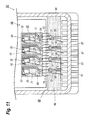
- FIG. 11 magnifies a primary portion of an optical transmitter apparatus modified from the optical transmitter apparatus shown in FIG. 10 .
- FIG. 1 is a plan view of an optical module 1 A and FIG. 2 shows a cross section of the optical module 1 A taken along a line II-II indicated in FIG. 1 .
- the optical module 1 A of the present embodiment which may be implemented within an optical transmitter apparatus used in an optical communication system, includes a carrier 10 , a co-planar line 11 , a ground metal 13 , a bias pad 14 , a termination pad 15 , a side metal 16 , a back metal 17 , and a semiconductor element 20 .
- the semiconductor element 20 integrates a semiconductor laser diode (LD) monolithically with an optical modulator type of an electron-absorption (EA) on a substrate common to the LD and the EA.
- LD semiconductor laser diode
- EA electron-absorption
- the semiconductor element provides an anode pad 21 through which the LD is provided with a bias current and a signal pad 23 connected to an anode pad 22 of the EA, where the EA is driven by a driving signal provided through the signal pad 23 and the anode pad 22 .
- the anode pad 21 of the LD and the signal pad 23 may be formed by plated gold (Au).
- the carrier 10 which has a rectangular slab shape made of electrically insulating material but having a substantial thermal conductivity, includes a top surface 10 a , a back surface 10 b , sides, 10 c and 10 d , opposite to each other, and other sides, 10 e and 10 f , also opposite to each other.
- the former two sides, 10 c and 10 d longitudinally extend, white, the latter two sides, 10 e and 10 f , laterally extend and connect the former two sides, 10 c and 10 d .
- the carrier 10 mounts the semiconductor element 20 in a side closer to the side 10 e of the top surface 10 a .
- the carrier 10 may be made of, for instance, aluminum nitride (AlN) with a thickness T of greater than 0.3 mm.
- the carrier 10 of the present embodiment has the thickness of 0.4 mm.
- the co-planar line 11 comprises a signal line 12 and the ground metal 13 putting the signal line 12 therebetween.
- the signal line 12 which may be a metal pattern, longitudinally extends from the side 10 e to the other side 10 f along the side 10 c .
- the signal line 12 in one end thereof provides a pad 12 a to which a bonding wire is to be bonded, while in the other end thereof closer to the side 10 e also provides another pad 12 b to which another bonding wire 41 extending to the signal pad 23 is bonded.
- the signal line 12 extends along the side 10 c , which means that the signal line 12 and the semiconductor element 20 are arranged in side by side in an end closer to the side 10 e .
- the signal line 12 is bent in an end closer to the side 10 f , and the pad 12 a is arranged in a center but slightly shift closer to the side 10 c in the side 10 f.
- the signal line 12 is arranged closer to the side 10 c in a whole.
- the ground metal 13 which are a metal pattern, extends in respective sides of the signal line 12 leaving a predetermined gap therebetween.
- the optical module 1 A of the present embodiment provides the ground metal 13 on the whole top surface 10 a of the carrier 10 except for areas surrounding the signal line 12 , the bias pad 14 , and the termination pad 15 .
- the ground metal 13 in a portion closer to the side 10 d provides an area B 1 that mounts the semiconductor element 20 thereon such that the semiconductor element 20 in a back metal, which is a cathode electrode common to the LD and the EA, is physically and electrically connected to the ground metal 13 .
- the ground metal 13 also provides areas B 2 in respective sides of the signal line 12 in the side 10 f , to which bonding wires 73 are wire-bonded, which will be described later.
- the bias pad 14 which is a metal pattern, may be arranged in a longitudinal center close to the side 10 d .
- a bonding wire 43 electrically connects the bias pad 14 to the anode pad 21 .
- another bonding wire connects the bias pad 14 to a lead terminal provided in a package within which the optical module 1 A is enclosed, which will be illustrated in FIG. 3 .
- the termination pad 15 which is also a metal pattern isolated from the ground metal 13 , is arranged in the side 10 d and close to the side 10 e .
- a bonding wire 42 electrically connects the termination pad 15 to the signal pad 23 .
- a terminator 31 which is a resistor chip, connects the termination pad 15 to the ground metal. That is, the signal pad 23 of the BA is terminated by the terminator 31 through the bonding wire 42 and the termination pad 15 .
- the back metal 17 is provided in the back surface 10 b in a whole of the carrier 10 .
- the back metal 17 is only connected to the ground metal in the top surface 10 a of the carrier but floated from a chassis ground of the package. That is, the optical module 1 A shown in FIG. 1 is mounted on an electrically insulating plate provided on a thermo-electric cooler (TEC) 68 that provides a metal pattern reflecting dimensions of the back metal 17 of the carrier for mounting the carrier 10 thereon.
- TEC thermo-electric cooler
- the back metal 17 is floated from the chassis ground, and electrically connected only to the ground metal 13 , which is the signal ground, on the top surface 10 a of the carrier. Accordingly, the back metal 17 is sometimes called as a float metal in the present specification.
- the carrier 10 provides the back metal 17 . That is, to bond the carrier 10 in the back surface thereof 10 b onto the metal pattern provided in the electrically insulating top plate of the TEC. Another reason why the carrier 10 provides the back metal 17 is for testing the semiconductor element 20 during an assembly of the optical module 1 A. That is, in advance to install the optical module 1 A within the package, electrical tests of the LD and EA are carried out by probing the signal line 12 between the end pad 12 a and the ground metal 13 , and between the bias pad 14 and the ground metal 13 .
- static characteristic of the LD is investigated by supplying a DC bias between the bias pad 14 and the ground metal 13 as supplying a DC or a low frequency signal between the end pad 12 a of the signal line 12 and the ground metal 13 .
- dynamic characteristic of the PA is tested by supplying a high frequency signal between the end pad 12 a and the ground metal 13 as supplying a DC bias between the bias pad 14 and the ground metal 13 .
- complex probing is required for the test during the assembly of the optical module 1 A. Placing the carrier 10 with the back metal 17 on an electrically conductive substrate during the test, the probing to the ground metal 13 may be replaced to probe the electrically conductive substrate by connecting the back metal 17 to the ground metal 13 by the side metal 16 .
- the intermediate test during the assembly may be simplified.
- the back metal 17 possibly changes propagation characteristics of the driving signal carried on the signal line 12 when the back metal 17 is electrically connected to the chassis ground.
- noises externally entering the package possibly influence the driving signal on the signal line 12 through the chassis ground, the back metal 17 and the ground metal 13 .
- the back metal 17 is preferably isolated from the chassis ground.
- the side metal 16 is provided only in the side 10 d of the carrier in a portion closer to the side 10 f . That is, the side 10 d removes the side metal 16 in a portion closer to the side 10 e . Because the side metal 16 is apart from the signal line 12 , the side metal 16 causes no influence of the transmission of the driving signal carried on the signal line 12 .
- the signal line 12 , the ground metal 13 , the bias pad 14 , the termination pad 15 , the side metal 16 , and the back metal 17 may be made of plated gold (Au) accompanying with a titanium (Ti) layer, a platinum (Pt) layer, and another gold (Au) layer as seed layers for the metal plating.
- Ti titanium
- Pt platinum
- Au gold
- the Ti layer, the Pt layer, and the Au layer have thicknesses of 0.1 ⁇ m, 0.2 ⁇ m, and 3 ⁇ m, respectively.
- FIG. 3 shows a plan view of an optical transmitter apparatus 2 A that implements the optical module 1 A therein.
- the optical transmitter apparatus 2 A includes, in addition to the optical module 1 A, a package 61 , a lens 32 , a wiring substrate 63 , and a thermoelectric cooler 68 therein.
- the package 61 which has a box shape, encloses the optical module 1 A, the lens 32 , the wiring substrate 63 , and the TEC 68 air-tightly.
- the package 61 provides a feedthrough 69 and lead terminals 67 in a rear thereof.
- the feedthrough 69 provides another co-planar line also comprised of a signal line 65 and ground metal 66 sandwiching the signal line therebetween.
- the lead terminals 67 are formed on a ceramic layer extending from an interior to an exterior of the package 61 .
- FIG. 3 only illustrates a top surface of the ceramic layer, the ceramic layer provides other lead terminals connected to the signal line 65 in a back surface thereof, which also extends from the interior to the exterior of the package 61 .
- the lens 32 which is also mounted on the TEC 68 , optically couples with an output facet of the semiconductor element 20 .
- the lens 32 collimates light L 1 emitted from the semiconductor element 20 .
- the collimated light L 1 is externally output from the package 61 through a window 70 provided in a front side of the package 61 .
- the wiring substrate 63 which is arranged between the feedthrough 69 and the optical module 1 A and mounted on the TEC 68 , provides a co-planar line comprising a signal line 63 a and ground metal 63 b sandwiching the signal line 63 a therebetween.
- One end of the signal line 63 a is wire-bonded to the end pad 12 a of the signal line 12 on the carrier 10 by a bonding wire 73
- the other end of the signal line 63 a is wire-bonded to the signal line 65 on the feedthrough 69 by a bonding wire 77 .
- the driving signal may be provided to, the signal pad 23 of the EA through one of the lead terminal 67 , the signal line 65 of the feedthrough 69 , the bonding wire 77 , the signal line 63 a on the wiring substrate 63 , the bonding wire 73 , the signal line 12 on the carrier 10 , and the bonding wire 41 .
- the ground metal 63 b is formed in the respective sides of the signal line 63 a as leaving a predetermined gap therebetween and wire-bonded to the ground metal 13 on the carrier 10 with bonding wires 74 . Also, other ends of the ground metal 63 b is wire-bonded to the ground metal 66 on the feedthrough 69 with bonding wires, 75 and 76 , and the ground metal. 66 on the feedthrough 69 is electrically and externally connected to the signal ground of a system where the optical transmitter apparatus 2 A is implemented therein.
- the ground metal 63 b on the wiring substrate 63 mounts a capacitor 64 of a type of a die-capacitor with a bottom electrode facing and in contact to the ground metal 63 b , while, a top electrode thereof is wire-bonded to the lead terminal 67 with a bonding wire 72 and to the bias pad 14 on the carrier 10 with another bonding wire 71 .
- the lead terminal 67 receives a DC bias and this DC bias is supplied to the semiconductor element 20 , in particular, to the anode pad 21 of the LD through the bonding wire 72 , the bypassing capacitor 64 , the bonding wire 71 , the bias pad 14 and the bonding wire 43 .
- the optical module 1 A of the embodiment provides the carrier 10 whose back surface 10 b is coated with the back metal 17 .
- the back metal 17 is only for testing the optical module 1 A during the assembly thereof and electrically connected to nowhere except for the ground metal 13 on the top surface 10 a of the carrier after the completion of the assembly.
- the back metal 17 is electrically connected to the ground metal 13 on the top surface 10 a through the side metal 16 .
- the back metal 17 is physically connected to the top plate of the TEC 68 made of electrically insulating material. Thus, the back metal 17 causes no influence for the electrical transmission of the driving signal on the signal line 12 .
- the signal line 12 may be the co-planar line combined only with the ground metal 13 provided in the respective sides thereof as leaving the gap therebetween.
- the back, metal 17 is useful for the test during the assembly of the optical transmitter apparatus 2 A. That is, the optical module 1 A, in particular, the semiconductor element 20 , is necessary to be tested in the static characteristic in the LD and the EA, namely, the I-L characteristic of the LD and the extinction ratio of the EA, and the temperature dependence thereof; and the dynamic characteristic of the EA, namely, the frequency dependence of the extinction ratio of the EA.
- the optical module 1 A is mounted on a stage of the testing apparatus and probing the bias pad 14 and the stage for the test of the LD and the end pad 12 a of the signal line 12 and the stage for the EA, the test procedures may be simplified and the test may be accelerated.
- the side metal 16 of the embodiment may electrically connect the back metal 17 to the ground metal 13 .
- the carrier 10 provides the side metal 16 only in the side 10 d apart enough from the signal line 12 compared with the thickness T of the carrier 10 .
- the back metal 17 may be electrically connected to the ground metal 13 without influencing the signal transmission on the signal line 12 , in particular, the high frequency performance of the driving signal carried on the signal line 12 .
- the carrier 10 has the thickness T preferably greater than 0.3 mm, where the present embodiment of the carrier 10 has the thickness of 0.4 mm.
- the back metal 17 may be set apart from the signal line at least 0.3 mm. Accordingly, the back metal 17 causes no influence for the co-planar arrangement of the signal line 12 and the top ground metal 13 .
- the carrier 10 of the embodiment is made of aluminum nitride (AlN)
- AlN aluminum nitride
- the back metal 17 possibly causes or degrades the co-planar characteristic on the top surface 10 a when the thickness T of the carrier becomes less than 0.15 mm.
- the carrier 10 with the thickness T greater than 0.3 mm the back metal 17 may cause substantially no influence on the transmission of the driving signal on the signal line 12 .
- FIGS. 4 and 5 show a plan view of the optical module 1 B and a cross section thereof taken along the line V-V indicated in FIG. 4 , respectively.
- the optical module 1 B in particular, the carrier 10 B provides, instead of the side metal 16 in the aforementioned embodiment, vias 18 in respective sides of the signal line 12 and in an area for wire-bonding to the wiring substrate 63 .
- the vias 18 are filled with a metal to secure electrical conductivity thereof.
- the carrier 10 B in FIG. 4 provides only three vias 18 , the carrier 10 B may provide four or more vias to securely connect the back metal 17 to the top ground 13 .
- FIGS. 6 and 7 show a plan view of the optical module 1 C and a cross section thereof taken along the line VII-VII appearing in FIG. 6 , respectively.
- the optical module 1 C shown in FIGS. 6 and 7 in particular, the carrier 10 C provides a side metal 19 in a whole of the side 10 c from the side 10 e to the other side 10 f , where the side 10 c is closer to the co-planar arrangement 11 different from the arrangement of the carrier 10 shown in FIG. 1 .
- the co-planar line 11 possibly degrades the transmission characteristic thereof such as S-parameters, namely, varies the transmission impedance thereof from designed impedance. Accordingly, taking the thickness T of the carrier 10 C, a distance from the signal line 12 to the side metal 19 is greater than the predetermined gap left between the signal line 12 and the ground metal 13 .
- the sides 10 e and/or 10 f may also provide a side metal electrically connecting the back metal 17 to the ground 13 . Similar to the previous modifications, a distance from the signal line 12 to the side metal provided in the sides, 10 e and/or 10 f , is greater than the predetermined gap between the signal line 12 and the ground metal 13 .
- FIG. 8A and FIG. 8B compare the transmission impedance of the co-planar line 11 of the first embodiment shown in FIG. 1 and that of the second modification shown in FIG. 6 . That is, FIGS. 8A and 8B compare the influence of the side metals, 16 and 19 , provided apart from the signal line 12 ( FIG. 8B ) and closer to the signal line 12 ( FIG. 8A ), respectively.
- the S-parameter S 11 is requested to be not only low enough, which means that the transmission impedance of the co-planar line 11 becomes equal to the designed characteristic impedance, but smooth enough in an operating frequency range.
- FIGS. 8A and FIG. 8B compare the transmission impedance of the co-planar line 11 of the first embodiment shown in FIG. 1 and that of the second modification shown in FIG. 6 . That is, FIGS. 8A and 8B compare the influence of the side metals, 16 and 19 , provided apart from the signal line 12 ( FIG. 8B ) and closer to the signal line 12 ( FIG. 8A ),
- the signal reflection S 11 causes a substantial dip in frequencies around 25 GHz, which is a high end of the operating frequency range for the optical modules, 1 A and 1 B.
- the dip in the signal reflection S 11 means that, although the smoothness thereof is slightly sacrificed, the characteristic impedance of the co-planar line 11 becomes closer to the designed one.
- the amount of the dip is within an acceptable range for the practical operation of the optical module 1 C.
- the carrier 10 of the embodiment may provide a side metal in the side 10 f and in the other side 10 e as long as the gap with a minimum distance at least 0.15 mm is secured against the signal line 12 .
- FIG. 9 shows a plan view of an optical transmitter apparatus 2 B according to the second embodiment of the present invention.
- the optical transmitter apparatus 2 B implements four optical modules 1 A and four lenses 32 within the package 61 , where a unit of one optical module 1 A including one semiconductor element 20 and one lens 32 constitute one lane of the optical transmitter apparatus 2 B.
- Each of the lanes is independently driven by a driving signal supplied from the outside of the package 61 through the co-planar lines.
- FIG. 9 explicitly shows that optical modules installed within the optical transmitter apparatus 2 B are the type of the first embodiment 1 A shown in FIG. 1 , other types of the optical module, 1 B and 1 C, may be implemented within the optical transmitter apparatus 2 B.
- the rear end of the package 61 opposite to those installing the lenses 32 provides lead terminals 67 through which the driving signals for the respective lanes are provided.
- the lead terminals 67 appearing in FIG. 9 are grouped in two types, one of which are for providing the driving signals while others secure the ground, where they are alternately disposed to each other.
- the lead terminals involved within the former group continue to the signal lines 65 on the feedthrough 69 and those within the latter group continue to the ground metal 66 also provided on the feedthrough 69 .
- the signal lines 65 are wire-bonded to the signal lines 63 a on the wiring substrate 63 . Similar to the first embodiment shown in FIG. 3 , the wiring substrate 63 , the optical modules 1 A and the lenses 32 are mounted on the top plate of the TEC 68 , where the top plate is made of electrically insulating material.
- FIG. 10 magnifies a primary portion of the optical transmitter apparatus 2 B, that is, the arrangement on the wiring substrate 63 and four optical modules 1 A mounted on the TEC 68 .
- the wiring substrate 63 provides four co-planar lines, that is, four signal lines 63 a and the ground metal 63 b between the signal lines 63 a leaving the gap of the predetermined distance therebetween.
- the signal lines 63 a in one ends 63 e are wire-bonded to the signal lines 65 on the feedthrough 69 by bonding wires 77 .
- the ground metals 63 b are wire-bonded to the ground metals 66 on the feedthrough 69 by bonding wires, 75 and 76 .
- the ground metals 66 on the feedthrough 69 are connected to the signal ground provided outside of the package 61 but isolated from the chassis ground of the package 61 .
- the wiring substrate 63 also mounts on the ground metal 63 b four capacitors 64 that correspond to the respective lanes.
- the capacitors 64 are the type of a die-capacitor having a top electrode and a bottom electrode.
- the bottom electrode faces and in contact to the ground metal 63 b , while, the top electrode is wire-bonded to the lead terminals 67 with bonding wires 72 , where the terminals 67 supply the DC biases, and also to the bias pads 14 on the optical modules 1 A with bonding wires 71 .
- the optical modules 1 A each has an arrangement shown in FIG. 1 , that is, the optical modules 1 A each has the lateral width smaller than 1 mm, the present embodiment has the lateral with of 0.7 mm, and the longitudinal length of about 2 mm.
- Four optical modules 1 A are arranged in side by side such that a total lateral width thereof is within about 3 mm, which means that a gap about 0.07 mm is secured therebetween.
- Each of the optical modules 1 A provides the carrier 10 with the top surface 10 a and the back surface 10 b .
- the back surface 10 h accompanies with the back metal 17
- the top surface 10 a provides the ground metal 13 and the signal line 12 that form the co-planar line 11 .
- the ground metal 13 mounts the semiconductor element 20 thereon.
- the top surface 10 a also provides the bias pad 14 and the termination pad 15 .
- the co-planar line 11 and the semiconductor element 20 are disposed in side by side in the side 10 e facing the lens 32 , while, the co-planar line 11 is disposed in a center portion in the side 10 f facing the wiring substrate 63 .
- the semiconductor element 20 of the present embodiment integrates the LD with the EA, where the LD emits the continuous wave (CW) light while the EA modulates this CW light.
- the semiconductor element 20 may output the modulated light to the lens 32 .
- the lens 32 may collimate the modulated light that is dispersive from the semiconductor element 20 .
- the optical transmitter apparatus 2 B provides an optical coupling system that multiplexes the four collimated light output from the lenses 32 into one multiplexed light.
- the multiplexed light is output from the package 61 passing through the window 70 in the front wall of the package 61 .
- the co-planar line 11 carries the driving signal thereon to the semiconductor element 20 , specifically, to the signal pad 23 of the EA in the semiconductor element 20 .
- the co-planar line 11 in one end 12 a thereof locates in a center portion in the side 10 f facing the wiring substrate 63 , exactly, in the center portion but slightly closer to the side 10 c , while the co-planar line 11 in the other end 12 b thereof and the semiconductor elements 20 are arranged in side by side in the side 10 e facing the lens 32 . Accordingly, the signal line 12 of the co-planar line 11 runs along the side 10 c of the carrier 10 as a whole.
- the signal line from the co-planar line 11 to the termination resistor 31 crosses the semiconductor element 20 in the side of the EA thereof through two bonding wires, 41 and 42 .
- the driving signal in the present embodiment has the speed of, for instance, 28 Gb/s. Because the bonding wires, 41 and 42 , extend in perpendicular to the signal line 12 provided in the neighbor optical modules, the crosstalk between the bonding wires, 41 and 42 , and the neighbor signal lines 12 may be suppressed.
- the present optical transmitter apparatus 2 B arranges the optical modules 1 A in side by side with an extremely limited spaces therebetween; accordingly, arrangements of the optical modules, 1 A may suppress the crosstalk between the lanes is inevitable.
- one portion of the ground metal 13 closer to the side 10 c has a width narrower than a width of the other portion of the ground metal 13 in the side of the bias pad 14 and the terminator pad 15 .
- the narrower ground metal 13 preferably extends more than a half of the side 10 c .
- the narrower ground metal 13 closer to the sides 10 c has an average width thereof that is narrower than an average width of the ground metal 13 disposed in the opposite side.
- the signal line 12 is bent toward the center portion in the side closer to the side 10 f of the carrier 10 . That is, the signal line 12 becomes gradually apart from the side 10 c as close to the side 10 f .
- the narrower ground metal 13 has a width w 1 at the side 10 f that is wider than a width w 2 thereof at the side 10 e ; but the width w 2 of the narrower ground metal 13 is wider than a width w 3 of the signal line.
- a co-planar line generally has a ground metal in respective sides of the signal line have widths wider enough compared to a width of the signal line.
- the arrangement of the co-planar line of the present embodiment, opposite to the conventional arrangement for the co-planar line, has the signal line whose width is wider than that of the ground line.
- the signal line 12 of the embodiment has the width w 3 of, for instance, smaller than 1/10 of the lateral width of the optical module 1 A, where the present embodiment provides the signal line 12 with the width about 70 ⁇ m and that of the narrower ground line 13 at the side 10 e has a width of 10 to 70 ⁇ m.
- This arrangement of the narrower ground metal 13 may be effective for reducing the crosstalk affected from an optical module arranged in the neighbor to the side 10 c in addition to the positional relation between the bonding wires, 41 and 42 , and the signal line 12 , which makes a substantially right angle therebetween.
- the signal pattern 12 , the ground metal 13 , and two pads, 14 and 15 may be made of plated gold (Au), exactly, a stacked seed metals of titanium (Ti), platinum (Pt), and gold (Au), and the plated gold (Au) thereof, with thicknesses of 0.1 ⁇ m, 0.2 ⁇ m, and 3 ⁇ m, respectively.
- the wiring substrate 63 provides four co-planar structures 63 c constituted by the signal lines 63 a and the ground metal 63 b sandwiching the signal lines 63 a therebetween.
- the wiring substrate 63 has a rectangular shape with a lateral width of 3.5 mm and a longitudinal length of 1.0 mm.
- the wiring substrate 63 also has a side 63 d facing the optical modules 1 A and another side 63 e facing the feedthrough 69 .
- the ground metal 63 b mounts the de-coupling capacitors 64 thereon.
- the de-coupling capacitors 64 and the co-planar structures 63 c are laterally and alternately arranged in side by side on the wiring substrate 63 .
- the signal lines 63 a have a pitch substantially equal to a pitch of the optical modules 1 A in the side 63 d thereof, while, another pitch in the side 63 e substantially equal to a pitch of the lead terminals 67 in the first group that carry the driving signals.
- the former pitch is smaller than the latter, that is, the wiring substrate 63 may show a function of the pitch-conversion.
- the signal lines 63 a provide pads 63 f in one ends facing the optical modules 1 A, while, other pads 63 g in other ends facing the feedthrough 69 .
- the former pads 63 f are wire-bonded to the pads 12 a in the optical modules 1 A with the bonding wires 73
- the latter pads 63 g are wire-bonded to the signal lines 65 on the feedthrough 69 with bonding wires 77 .
- the pads, 63 f and 63 g extend in the edges of the respective sides, 63 d and 63 e , which means that the four ground metals 63 b are isolated in the top surface 63 c of the wiring substrate 63 .
- the wiring substrate 63 similar to the optical modules 1 A, provides a back metal in a back surface thereof; and each of the ground metals 63 b provides vias 63 h that electrically connect the ground metals 63 b on the top surface to the back metal on the back surface of the wiring substrate.
- the ground metals 63 b are electrically connected to each other.
- the wiring substrate 63 is mounted on the top plate of the TEC, which may be made of electrically insulating materials but provides a metal pad that is electrically isolated from the chassis ground.
- the optical modules, 1 A to 1 C, of the present invention arranges the co-planar lines 11 closer to the side 10 c of the carriers 10 not a center thereof.
- the carrier 10 provides the metal in the side 10 c , or the side 10 d in the optical module 1 A arranged neighbor thereto, that connects the back metal 17 to the ground metal 13 on the top surface 10 a of the carrier 10 , the crosstalk, or the noise leaking from the signal line 12 to the semiconductor element 20 in the neighbor lane may be effectively reduced.
- the ground metal 13 along the side 10 c has the width w 2 smaller than the width w 3 of the signal line, which may further reduce high frequency components contained in the driving signal from leaking to the neighbor channel.
- the arrangement on the optical module 1 A of the embodiment may effectively eliminate the crosstalk between the lanes.
- the ground metal 13 with the width w 2 thereof narrower than the width w 3 of the signal line extends at least half of the side 10 c .
- an average width of the ground metal in the side 10 d is greater than an average width of the other ground metal 13 in the side 10 c , which may also effective reduce the crosstalk.
- the optical transmitter apparatus 2 B of the second embodiment mounts the die-capacitors 64 on the wiring substrate 63 .
- each of the optical modules 1 A may mount the die-capacitor 64 on the ground metal 13 thereon.
- each of the carrier 10 provide the side metal in at least one of the sides, 10 c or 10 d , thereof, that is, the side metals are provided between the signal lines 12 , the crosstalk between the lanes may be effectively suppressed. Because the die-capacitor 64 is mounted on the carrier 10 , a leaking path for high frequency components from the EA to the ground metal 13 through the die capacitor 64 may close within the optical module 1 A, the crosstalk of the high frequency components to the neighbor lanes may be suppressed.
- the leaking path from the EA to the ground metal 13 includes the bonding wire 74 that connects the ground metal 63 b on the wiring substrate 63 to the ground metal 13 on the carrier 10 , which may possibly degrade the crosstalk between the lanes.
- the optical transmitter apparatus 2 B of the present embodiment provides the wiring substrate 63 between the feedthrough 69 and the optical modules 1 A; and the wiring substrate 63 may show the function of the pitch conversion. That is, the pitch of the signal lines 63 a in the side 63 e facing the feedthrough 69 is set wider than the pitch of the signal lines 63 a in the side 63 d facing the optical modules 1 A.
- the optical module 1 B may remove the wiring substrate 63 by arranging an optical modules 1 E in the pitch corresponding to the pitch of the lead terminals 67 for the driving signals, or setting the function of the pitch conversion in the signal lines 65 on the feedthrough 69 ; and mounting the die-capacitors 64 on the respective optical modules 1 E.
- FIG. 11 shows such an arrangement of the optical transmitter apparatus 2 C according to a modification of the optical transmitter apparatus 2 B shown in FIG. 9 .
- the optical transmitter apparatus 2 C removes the wiring substrate 63 and disposes the optical modules 1 E by a pitch substantially equal to the pitch of the lead terminals 67 in the first group for the driving signals. Because the pitches in the optical modules 1 E and the lead terminals 67 are comparable to each other, the signal lines 65 on the feedthrough 69 extend substantially straight, which means that the lengths of the signal lines 65 become minimum such that the degradation in the shapes of the driving signals may be effectively reduced.
- the optical modules 1 E shown in FIG. 11 have a feature that the bias pads 14 provided on the top of the carriers 10 disappear.
- the biases supplied to the LD are directly provided from the die-capacitors 64 through the bonding wires 71 without interposing the bias pads 14 .
- This arrangement of the removal of the bias pads 14 enables that the side metal in the side 10 d of the carrier extends from the edge 10 f facing the feedthrough 69 to an end of the ground metal facing the terminator pad 15 , that is, almost all of the side 10 f is covered with the side metal.
- the side metal in the side 10 f connected to the ground metal 13 may be put between the signal lines 12 ; the crosstalk between the lanes may be further eliminated.
- the arrangement of the modified optical transmitter apparatus 2 C may form a wider space for mounting the optical coupling system in front of the optical modules 1 E, where the optical coupling system optically couples the semiconductor elements 20 with the optical fiber set in the window 70 .
- such an arrangement may narrower a size of the top plate of the TEC 68 which may save the power consumption of the TEC 68 .
Landscapes
- Physics & Mathematics (AREA)
- Electromagnetism (AREA)
- Condensed Matter Physics & Semiconductors (AREA)
- General Physics & Mathematics (AREA)
- Optics & Photonics (AREA)
- Engineering & Computer Science (AREA)
- Computer Networks & Wireless Communication (AREA)
- Signal Processing (AREA)
- Semiconductor Lasers (AREA)
Priority Applications (1)
| Application Number | Priority Date | Filing Date | Title |
|---|---|---|---|
| US16/209,231 US10411432B2 (en) | 2016-04-25 | 2018-12-04 | Optical transmitter providing coplanar line on carrier |
Applications Claiming Priority (4)
| Application Number | Priority Date | Filing Date | Title |
|---|---|---|---|
| JP2016-087091 | 2016-04-25 | ||
| JP2016087091 | 2016-04-25 | ||
| JP2016-087092 | 2016-04-25 | ||
| JP2016087092 | 2016-04-25 |
Related Child Applications (1)
| Application Number | Title | Priority Date | Filing Date |
|---|---|---|---|
| US16/209,231 Continuation US10411432B2 (en) | 2016-04-25 | 2018-12-04 | Optical transmitter providing coplanar line on carrier |
Publications (2)
| Publication Number | Publication Date |
|---|---|
| US20170310078A1 US20170310078A1 (en) | 2017-10-26 |
| US10177529B2 true US10177529B2 (en) | 2019-01-08 |
Family
ID=60089101
Family Applications (2)
| Application Number | Title | Priority Date | Filing Date |
|---|---|---|---|
| US15/496,548 Active 2037-04-27 US10177529B2 (en) | 2016-04-25 | 2017-04-25 | Optical transmitter providing coplanar line on carrier |
| US16/209,231 Active US10411432B2 (en) | 2016-04-25 | 2018-12-04 | Optical transmitter providing coplanar line on carrier |
Family Applications After (1)
| Application Number | Title | Priority Date | Filing Date |
|---|---|---|---|
| US16/209,231 Active US10411432B2 (en) | 2016-04-25 | 2018-12-04 | Optical transmitter providing coplanar line on carrier |
Country Status (2)
| Country | Link |
|---|---|
| US (2) | US10177529B2 (zh) |
| CN (1) | CN107306009B (zh) |
Cited By (2)
| Publication number | Priority date | Publication date | Assignee | Title |
|---|---|---|---|---|
| DE102021104885A1 (de) | 2020-03-04 | 2021-09-09 | Schott Ag | Sockel und Gehäuse mit integriertem Kühler für elektronische Bauelemente |
| DE102020120167A1 (de) | 2020-07-30 | 2022-02-03 | Schott Ag | Gehäuse, vorzugsweise TO-Gehäuse, Sockel für Gehäuse und Baugruppe mit einem solchen Gehäuse und/oder Sockel |
Families Citing this family (15)
| Publication number | Priority date | Publication date | Assignee | Title |
|---|---|---|---|---|
| JP2018074057A (ja) * | 2016-11-01 | 2018-05-10 | 住友電工デバイス・イノベーション株式会社 | 半導体レーザキャリア組立体、光半導体装置、及び光半導体装置の製造方法 |
| CN109638638B (zh) | 2017-10-05 | 2023-06-13 | 住友电工光电子器件创新株式会社 | 光学模块 |
| JP6988493B2 (ja) | 2018-01-11 | 2022-01-05 | 住友電気工業株式会社 | 光モジュール及びその製造方法 |
| CN111801842B (zh) * | 2018-03-07 | 2022-03-22 | 住友电工光电子器件创新株式会社 | 半导体装置 |
| US10374386B1 (en) * | 2018-06-07 | 2019-08-06 | Finisar Corporation | Chip on carrier |
| US10547158B1 (en) * | 2018-10-31 | 2020-01-28 | Avago Technologies International Sales Pte. Limited | Optical communication device and system |
| KR102388885B1 (ko) | 2018-11-06 | 2022-04-20 | 미쓰비시덴키 가부시키가이샤 | 광 반도체 장치, 광 모듈 및 광 반도체 장치의 제조 방법 |
| JP7416435B2 (ja) * | 2018-12-26 | 2024-01-17 | 住友電工デバイス・イノベーション株式会社 | 光半導体装置 |
| WO2020133381A1 (zh) * | 2018-12-29 | 2020-07-02 | 泉州三安半导体科技有限公司 | 一种激光器封装结构 |
| CN110190504B (zh) * | 2019-05-24 | 2020-12-15 | 宁波东立创芯光电科技有限公司 | 半导体激光器阵列封装结构 |
| CN112467513A (zh) * | 2019-08-22 | 2021-03-09 | 住友电工光电子器件创新株式会社 | 光学半导体装置和载体 |
| JP7474112B2 (ja) * | 2020-05-15 | 2024-04-24 | CIG Photonics Japan株式会社 | 光モジュール |
| US11178473B1 (en) * | 2020-06-05 | 2021-11-16 | Marvell Asia Pte, Ltd. | Co-packaged light engine chiplets on switch substrate |
| US11165509B1 (en) | 2020-06-05 | 2021-11-02 | Marvell Asia Pte, Ltd. | Method for co-packaging light engine chiplets on switch substrate |
| JP2023005501A (ja) * | 2021-06-29 | 2023-01-18 | 新光電気工業株式会社 | 半導体パッケージ用ステム、半導体パッケージ |
Citations (8)
| Publication number | Priority date | Publication date | Assignee | Title |
|---|---|---|---|---|
| JPH05251939A (ja) | 1992-03-02 | 1993-09-28 | Mitsubishi Electric Corp | マイクロ波回路 |
| JP2001209017A (ja) | 1999-11-15 | 2001-08-03 | Mitsubishi Electric Corp | 光電変換半導体装置 |
| US20040264835A1 (en) * | 2002-08-29 | 2004-12-30 | Hitachi, Ltd. | Optical module and optical transmission apparatus |
| US20050213882A1 (en) * | 2004-02-19 | 2005-09-29 | Hisao Go | Optical sub-assembly having a thermo-electric cooler and an optical transceiver using the optical sub-assembly |
| US20070053639A1 (en) * | 2005-09-05 | 2007-03-08 | Mitsubishi Electric Corporation | Optical module |
| US20080196929A1 (en) * | 2007-02-15 | 2008-08-21 | Hisashi Takamatsu | Optical transmitter module |
| US20120128290A1 (en) * | 2010-11-19 | 2012-05-24 | Electronics And Telecommunications Research Institute | Optical modules |
| JP2015125153A (ja) | 2013-12-25 | 2015-07-06 | 日本電信電話株式会社 | 光モジュール |
Family Cites Families (5)
| Publication number | Priority date | Publication date | Assignee | Title |
|---|---|---|---|---|
| DE69721272T2 (de) * | 1997-11-11 | 2004-02-05 | Agilent Technologies Inc., A Delaware Corp., Palo Alto | Elektrische Isolierung optoelektronischer Bauelemente |
| JP2003509851A (ja) * | 1999-09-03 | 2003-03-11 | ザ リージェンツ オブ ザ ユニバーシティ オブ カリフォルニア | 一体型光学変調器を有する波長可変レーザソース |
| US6873449B1 (en) * | 2003-09-05 | 2005-03-29 | The Furukawa Electric Co., Ltd. | Signal transmission line for an optical modulator |
| GB2430548B (en) * | 2005-09-27 | 2011-08-10 | Agilent Technologies Inc | An integrated modulator-laser structure and a method of producing same |
| WO2014022971A1 (zh) * | 2012-08-07 | 2014-02-13 | 华为技术有限公司 | 外调制激光器、无源光通信设备及系统 |
-
2017
- 2017-04-24 CN CN201710273581.XA patent/CN107306009B/zh active Active
- 2017-04-25 US US15/496,548 patent/US10177529B2/en active Active
-
2018
- 2018-12-04 US US16/209,231 patent/US10411432B2/en active Active
Patent Citations (9)
| Publication number | Priority date | Publication date | Assignee | Title |
|---|---|---|---|---|
| JPH05251939A (ja) | 1992-03-02 | 1993-09-28 | Mitsubishi Electric Corp | マイクロ波回路 |
| JP2001209017A (ja) | 1999-11-15 | 2001-08-03 | Mitsubishi Electric Corp | 光電変換半導体装置 |
| US6437899B1 (en) | 1999-11-15 | 2002-08-20 | Mitsubishi Denki Kabushiki Kaisha | Opto-electric conversion semiconductor device |
| US20040264835A1 (en) * | 2002-08-29 | 2004-12-30 | Hitachi, Ltd. | Optical module and optical transmission apparatus |
| US20050213882A1 (en) * | 2004-02-19 | 2005-09-29 | Hisao Go | Optical sub-assembly having a thermo-electric cooler and an optical transceiver using the optical sub-assembly |
| US20070053639A1 (en) * | 2005-09-05 | 2007-03-08 | Mitsubishi Electric Corporation | Optical module |
| US20080196929A1 (en) * | 2007-02-15 | 2008-08-21 | Hisashi Takamatsu | Optical transmitter module |
| US20120128290A1 (en) * | 2010-11-19 | 2012-05-24 | Electronics And Telecommunications Research Institute | Optical modules |
| JP2015125153A (ja) | 2013-12-25 | 2015-07-06 | 日本電信電話株式会社 | 光モジュール |
Cited By (4)
| Publication number | Priority date | Publication date | Assignee | Title |
|---|---|---|---|---|
| DE102021104885A1 (de) | 2020-03-04 | 2021-09-09 | Schott Ag | Sockel und Gehäuse mit integriertem Kühler für elektronische Bauelemente |
| US20210281042A1 (en) * | 2020-03-04 | 2021-09-09 | Schott Ag | Header and package with integrated cooler for electronic components |
| DE102020120167A1 (de) | 2020-07-30 | 2022-02-03 | Schott Ag | Gehäuse, vorzugsweise TO-Gehäuse, Sockel für Gehäuse und Baugruppe mit einem solchen Gehäuse und/oder Sockel |
| WO2022023403A1 (en) | 2020-07-30 | 2022-02-03 | Schott Ag | Housing, preferably a transistor outline housing, socket for housing, and assembly comprising such a housing and/or socket |
Also Published As
| Publication number | Publication date |
|---|---|
| US20170310078A1 (en) | 2017-10-26 |
| US20190131762A1 (en) | 2019-05-02 |
| CN107306009B (zh) | 2021-04-13 |
| CN107306009A (zh) | 2017-10-31 |
| US10411432B2 (en) | 2019-09-10 |
Similar Documents
| Publication | Publication Date | Title |
|---|---|---|
| US10411432B2 (en) | Optical transmitter providing coplanar line on carrier | |
| JP4923542B2 (ja) | 光素子用ステムとこれを用いた光半導体装置 | |
| US7317742B2 (en) | Optical sub-assembly having a thermo-electric cooler and an optical transceiver using the optical sub-assembly | |
| US7130100B2 (en) | Optical module | |
| US10416400B2 (en) | Semiconductor module | |
| JP3553222B2 (ja) | 光変調器モジュール | |
| US6599032B1 (en) | Transmitter/receiver for optical parallel transmission and board for optical module | |
| US20080196929A1 (en) | Optical transmitter module | |
| JP6881745B2 (ja) | 光半導体装置 | |
| US6567439B1 (en) | Radio-frequency laser module and a method for producing it | |
| US20240097399A1 (en) | Semiconductor laser light source device | |
| JP2020178117A (ja) | 光変調器キャリア組立体及び光モジュール | |
| JP2017199906A (ja) | 光半導体装置 | |
| JPH10275957A (ja) | 光半導体チップキャリア | |
| US11811191B2 (en) | Optical semiconductor device and carrier | |
| US6796723B2 (en) | Submount for opto-electronic module and packaging method using the same | |
| JP2004093606A (ja) | 光モジュール及び光伝送装置 | |
| CN114142335A (zh) | 用于电子元件的接头 | |
| JP7020590B1 (ja) | レーザ光源装置 | |
| US20220149592A1 (en) | Optical semiconductor module | |
| US7391099B2 (en) | Optical modulator module | |
| US11398866B2 (en) | Optical semiconductor device, optical transmission module, and optical transceiver | |
| JP7264320B1 (ja) | 半導体レーザ光源装置 | |
| JP2000164970A (ja) | 光素子モジュール | |
| US11722221B2 (en) | Optical module |
Legal Events
| Date | Code | Title | Description |
|---|---|---|---|
| AS | Assignment |
Owner name: SUMITOMO ELECTRIC DEVICE INNOVATIONS, INC., JAPAN Free format text: ASSIGNMENT OF ASSIGNORS INTEREST;ASSIGNOR:HIRAYAMA, MASAHIRO;REEL/FRAME:042138/0745 Effective date: 20170421 |
|
| STCF | Information on status: patent grant |
Free format text: PATENTED CASE |
|
| MAFP | Maintenance fee payment |
Free format text: PAYMENT OF MAINTENANCE FEE, 4TH YEAR, LARGE ENTITY (ORIGINAL EVENT CODE: M1551); ENTITY STATUS OF PATENT OWNER: LARGE ENTITY Year of fee payment: 4 |