US10037924B2 - Fin-FET device and fabrication method thereof - Google Patents
Fin-FET device and fabrication method thereof Download PDFInfo
- Publication number
- US10037924B2 US10037924B2 US15/287,302 US201615287302A US10037924B2 US 10037924 B2 US10037924 B2 US 10037924B2 US 201615287302 A US201615287302 A US 201615287302A US 10037924 B2 US10037924 B2 US 10037924B2
- Authority
- US
- United States
- Prior art keywords
- layer
- fin
- ions
- covering layer
- covering
- Prior art date
- Legal status (The legal status is an assumption and is not a legal conclusion. Google has not performed a legal analysis and makes no representation as to the accuracy of the status listed.)
- Active
Links
- 238000000034 method Methods 0.000 title claims abstract description 164
- 238000004519 manufacturing process Methods 0.000 title description 16
- 230000008569 process Effects 0.000 claims abstract description 117
- -1 titanium ions Chemical class 0.000 claims abstract description 105
- 229910052751 metal Inorganic materials 0.000 claims abstract description 95
- 239000002184 metal Substances 0.000 claims abstract description 95
- 229910021332 silicide Inorganic materials 0.000 claims abstract description 88
- FVBUAEGBCNSCDD-UHFFFAOYSA-N silicide(4-) Chemical compound [Si-4] FVBUAEGBCNSCDD-UHFFFAOYSA-N 0.000 claims abstract description 88
- 238000000137 annealing Methods 0.000 claims abstract description 24
- 239000010936 titanium Substances 0.000 claims abstract description 20
- 229910052719 titanium Inorganic materials 0.000 claims abstract description 20
- 230000004888 barrier function Effects 0.000 claims description 83
- 150000002500 ions Chemical class 0.000 claims description 55
- 238000002955 isolation Methods 0.000 claims description 50
- 229910052796 boron Inorganic materials 0.000 claims description 34
- 229910052732 germanium Inorganic materials 0.000 claims description 33
- 239000000758 substrate Substances 0.000 claims description 29
- 229910000577 Silicon-germanium Inorganic materials 0.000 claims description 22
- 238000005137 deposition process Methods 0.000 claims description 18
- 230000007423 decrease Effects 0.000 claims description 7
- 238000005530 etching Methods 0.000 claims description 7
- 239000004020 conductor Substances 0.000 claims description 4
- RTAQQCXQSZGOHL-UHFFFAOYSA-N Titanium Chemical compound [Ti] RTAQQCXQSZGOHL-UHFFFAOYSA-N 0.000 abstract description 2
- 239000004065 semiconductor Substances 0.000 description 43
- 229910052814 silicon oxide Inorganic materials 0.000 description 22
- VYPSYNLAJGMNEJ-UHFFFAOYSA-N Silicium dioxide Chemical compound O=[Si]=O VYPSYNLAJGMNEJ-UHFFFAOYSA-N 0.000 description 17
- 239000000463 material Substances 0.000 description 17
- 238000005229 chemical vapour deposition Methods 0.000 description 11
- 239000007789 gas Substances 0.000 description 11
- 229910052710 silicon Inorganic materials 0.000 description 11
- GNPVGFCGXDBREM-UHFFFAOYSA-N germanium atom Chemical compound [Ge] GNPVGFCGXDBREM-UHFFFAOYSA-N 0.000 description 10
- 238000005468 ion implantation Methods 0.000 description 9
- XUIMIQQOPSSXEZ-UHFFFAOYSA-N Silicon Chemical compound [Si] XUIMIQQOPSSXEZ-UHFFFAOYSA-N 0.000 description 8
- 238000000231 atomic layer deposition Methods 0.000 description 8
- 238000005240 physical vapour deposition Methods 0.000 description 8
- 230000015572 biosynthetic process Effects 0.000 description 7
- 238000001312 dry etching Methods 0.000 description 7
- 239000010703 silicon Substances 0.000 description 7
- 229910004205 SiNX Inorganic materials 0.000 description 6
- UGACIEPFGXRWCH-UHFFFAOYSA-N [Si].[Ti] Chemical compound [Si].[Ti] UGACIEPFGXRWCH-UHFFFAOYSA-N 0.000 description 5
- 239000003989 dielectric material Substances 0.000 description 5
- 238000011065 in-situ storage Methods 0.000 description 5
- OAICVXFJPJFONN-UHFFFAOYSA-N Phosphorus Chemical compound [P] OAICVXFJPJFONN-UHFFFAOYSA-N 0.000 description 3
- LEVVHYCKPQWKOP-UHFFFAOYSA-N [Si].[Ge] Chemical compound [Si].[Ge] LEVVHYCKPQWKOP-UHFFFAOYSA-N 0.000 description 3
- 239000002800 charge carrier Substances 0.000 description 3
- 238000000151 deposition Methods 0.000 description 3
- 230000008021 deposition Effects 0.000 description 3
- 230000000694 effects Effects 0.000 description 3
- 229920002120 photoresistant polymer Polymers 0.000 description 3
- HBMJWWWQQXIZIP-UHFFFAOYSA-N silicon carbide Chemical compound [Si+]#[C-] HBMJWWWQQXIZIP-UHFFFAOYSA-N 0.000 description 3
- 229910010271 silicon carbide Inorganic materials 0.000 description 3
- 125000006850 spacer group Chemical group 0.000 description 3
- 239000000126 substance Substances 0.000 description 3
- ZOXJGFHDIHLPTG-UHFFFAOYSA-N Boron Chemical compound [B] ZOXJGFHDIHLPTG-UHFFFAOYSA-N 0.000 description 2
- BLRPTPMANUNPDV-UHFFFAOYSA-N Silane Chemical compound [SiH4] BLRPTPMANUNPDV-UHFFFAOYSA-N 0.000 description 2
- MJYCNMNFXMMHDL-UHFFFAOYSA-N [P].[Si].[Ti] Chemical compound [P].[Si].[Ti] MJYCNMNFXMMHDL-UHFFFAOYSA-N 0.000 description 2
- 238000000347 anisotropic wet etching Methods 0.000 description 2
- AIOWANYIHSOXQY-UHFFFAOYSA-N cobalt silicon Chemical compound [Si].[Co] AIOWANYIHSOXQY-UHFFFAOYSA-N 0.000 description 2
- 150000001875 compounds Chemical class 0.000 description 2
- 229910021419 crystalline silicon Inorganic materials 0.000 description 2
- 238000010586 diagram Methods 0.000 description 2
- 238000005516 engineering process Methods 0.000 description 2
- 239000012212 insulator Substances 0.000 description 2
- 230000010354 integration Effects 0.000 description 2
- 229910021645 metal ion Inorganic materials 0.000 description 2
- 229910021421 monocrystalline silicon Inorganic materials 0.000 description 2
- 229910052759 nickel Inorganic materials 0.000 description 2
- PEUPIGGLJVUNEU-UHFFFAOYSA-N nickel silicon Chemical compound [Si].[Ni] PEUPIGGLJVUNEU-UHFFFAOYSA-N 0.000 description 2
- 230000003647 oxidation Effects 0.000 description 2
- 238000007254 oxidation reaction Methods 0.000 description 2
- 229910052698 phosphorus Inorganic materials 0.000 description 2
- 238000000623 plasma-assisted chemical vapour deposition Methods 0.000 description 2
- 238000007517 polishing process Methods 0.000 description 2
- 229910021420 polycrystalline silicon Inorganic materials 0.000 description 2
- WGPCGCOKHWGKJJ-UHFFFAOYSA-N sulfanylidenezinc Chemical group [Zn]=S WGPCGCOKHWGKJJ-UHFFFAOYSA-N 0.000 description 2
- JBRZTFJDHDCESZ-UHFFFAOYSA-N AsGa Chemical compound [As]#[Ga] JBRZTFJDHDCESZ-UHFFFAOYSA-N 0.000 description 1
- 229910002601 GaN Inorganic materials 0.000 description 1
- 229910001218 Gallium arsenide Inorganic materials 0.000 description 1
- JMASRVWKEDWRBT-UHFFFAOYSA-N Gallium nitride Chemical compound [Ga]#N JMASRVWKEDWRBT-UHFFFAOYSA-N 0.000 description 1
- 229910003818 SiH2Cl2 Inorganic materials 0.000 description 1
- 229910003828 SiH3 Inorganic materials 0.000 description 1
- HZVLKSNOABSCQP-UHFFFAOYSA-N [Ti].[Ge].[Si] Chemical compound [Ti].[Ge].[Si] HZVLKSNOABSCQP-UHFFFAOYSA-N 0.000 description 1
- 229910052782 aluminium Inorganic materials 0.000 description 1
- 229910052785 arsenic Inorganic materials 0.000 description 1
- 229910052802 copper Inorganic materials 0.000 description 1
- 239000013078 crystal Substances 0.000 description 1
- 238000009713 electroplating Methods 0.000 description 1
- 230000009969 flowable effect Effects 0.000 description 1
- QUZPNFFHZPRKJD-UHFFFAOYSA-N germane Chemical compound [GeH4] QUZPNFFHZPRKJD-UHFFFAOYSA-N 0.000 description 1
- 229910052986 germanium hydride Inorganic materials 0.000 description 1
- 239000011521 glass Substances 0.000 description 1
- 230000006872 improvement Effects 0.000 description 1
- 229910001449 indium ion Inorganic materials 0.000 description 1
- 230000001939 inductive effect Effects 0.000 description 1
- 239000011261 inert gas Substances 0.000 description 1
- 238000005224 laser annealing Methods 0.000 description 1
- 230000004048 modification Effects 0.000 description 1
- 238000012986 modification Methods 0.000 description 1
- 238000007747 plating Methods 0.000 description 1
- 230000000717 retained effect Effects 0.000 description 1
- 229910021341 titanium silicide Inorganic materials 0.000 description 1
- 229910052721 tungsten Inorganic materials 0.000 description 1
Images


Classifications
-
- H—ELECTRICITY
- H01—ELECTRIC ELEMENTS
- H01L—SEMICONDUCTOR DEVICES NOT COVERED BY CLASS H10
- H01L21/00—Processes or apparatus adapted for the manufacture or treatment of semiconductor or solid state devices or of parts thereof
- H01L21/70—Manufacture or treatment of devices consisting of a plurality of solid state components formed in or on a common substrate or of parts thereof; Manufacture of integrated circuit devices or of parts thereof
- H01L21/77—Manufacture or treatment of devices consisting of a plurality of solid state components or integrated circuits formed in, or on, a common substrate
- H01L21/78—Manufacture or treatment of devices consisting of a plurality of solid state components or integrated circuits formed in, or on, a common substrate with subsequent division of the substrate into plural individual devices
- H01L21/82—Manufacture or treatment of devices consisting of a plurality of solid state components or integrated circuits formed in, or on, a common substrate with subsequent division of the substrate into plural individual devices to produce devices, e.g. integrated circuits, each consisting of a plurality of components
- H01L21/822—Manufacture or treatment of devices consisting of a plurality of solid state components or integrated circuits formed in, or on, a common substrate with subsequent division of the substrate into plural individual devices to produce devices, e.g. integrated circuits, each consisting of a plurality of components the substrate being a semiconductor, using silicon technology
- H01L21/8232—Field-effect technology
- H01L21/8234—MIS technology, i.e. integration processes of field effect transistors of the conductor-insulator-semiconductor type
- H01L21/823431—MIS technology, i.e. integration processes of field effect transistors of the conductor-insulator-semiconductor type with a particular manufacturing method of transistors with a horizontal current flow in a vertical sidewall of a semiconductor body, e.g. FinFET, MuGFET
-
- H—ELECTRICITY
- H01—ELECTRIC ELEMENTS
- H01L—SEMICONDUCTOR DEVICES NOT COVERED BY CLASS H10
- H01L21/00—Processes or apparatus adapted for the manufacture or treatment of semiconductor or solid state devices or of parts thereof
- H01L21/70—Manufacture or treatment of devices consisting of a plurality of solid state components formed in or on a common substrate or of parts thereof; Manufacture of integrated circuit devices or of parts thereof
- H01L21/77—Manufacture or treatment of devices consisting of a plurality of solid state components or integrated circuits formed in, or on, a common substrate
- H01L21/78—Manufacture or treatment of devices consisting of a plurality of solid state components or integrated circuits formed in, or on, a common substrate with subsequent division of the substrate into plural individual devices
- H01L21/82—Manufacture or treatment of devices consisting of a plurality of solid state components or integrated circuits formed in, or on, a common substrate with subsequent division of the substrate into plural individual devices to produce devices, e.g. integrated circuits, each consisting of a plurality of components
- H01L21/822—Manufacture or treatment of devices consisting of a plurality of solid state components or integrated circuits formed in, or on, a common substrate with subsequent division of the substrate into plural individual devices to produce devices, e.g. integrated circuits, each consisting of a plurality of components the substrate being a semiconductor, using silicon technology
- H01L21/8232—Field-effect technology
- H01L21/8234—MIS technology, i.e. integration processes of field effect transistors of the conductor-insulator-semiconductor type
- H01L21/8238—Complementary field-effect transistors, e.g. CMOS
- H01L21/823871—Complementary field-effect transistors, e.g. CMOS interconnection or wiring or contact manufacturing related aspects
-
- H—ELECTRICITY
- H01—ELECTRIC ELEMENTS
- H01L—SEMICONDUCTOR DEVICES NOT COVERED BY CLASS H10
- H01L21/00—Processes or apparatus adapted for the manufacture or treatment of semiconductor or solid state devices or of parts thereof
- H01L21/02—Manufacture or treatment of semiconductor devices or of parts thereof
- H01L21/04—Manufacture or treatment of semiconductor devices or of parts thereof the devices having potential barriers, e.g. a PN junction, depletion layer or carrier concentration layer
- H01L21/18—Manufacture or treatment of semiconductor devices or of parts thereof the devices having potential barriers, e.g. a PN junction, depletion layer or carrier concentration layer the devices having semiconductor bodies comprising elements of Group IV of the Periodic Table or AIIIBV compounds with or without impurities, e.g. doping materials
- H01L21/26—Bombardment with radiation
- H01L21/263—Bombardment with radiation with high-energy radiation
- H01L21/265—Bombardment with radiation with high-energy radiation producing ion implantation
- H01L21/26506—Bombardment with radiation with high-energy radiation producing ion implantation in group IV semiconductors
-
- H—ELECTRICITY
- H01—ELECTRIC ELEMENTS
- H01L—SEMICONDUCTOR DEVICES NOT COVERED BY CLASS H10
- H01L21/00—Processes or apparatus adapted for the manufacture or treatment of semiconductor or solid state devices or of parts thereof
- H01L21/02—Manufacture or treatment of semiconductor devices or of parts thereof
- H01L21/04—Manufacture or treatment of semiconductor devices or of parts thereof the devices having potential barriers, e.g. a PN junction, depletion layer or carrier concentration layer
- H01L21/18—Manufacture or treatment of semiconductor devices or of parts thereof the devices having potential barriers, e.g. a PN junction, depletion layer or carrier concentration layer the devices having semiconductor bodies comprising elements of Group IV of the Periodic Table or AIIIBV compounds with or without impurities, e.g. doping materials
- H01L21/28—Manufacture of electrodes on semiconductor bodies using processes or apparatus not provided for in groups H01L21/20 - H01L21/268
- H01L21/283—Deposition of conductive or insulating materials for electrodes conducting electric current
- H01L21/285—Deposition of conductive or insulating materials for electrodes conducting electric current from a gas or vapour, e.g. condensation
- H01L21/28506—Deposition of conductive or insulating materials for electrodes conducting electric current from a gas or vapour, e.g. condensation of conductive layers
- H01L21/28512—Deposition of conductive or insulating materials for electrodes conducting electric current from a gas or vapour, e.g. condensation of conductive layers on semiconductor bodies comprising elements of Group IV of the Periodic Table
- H01L21/28518—Deposition of conductive or insulating materials for electrodes conducting electric current from a gas or vapour, e.g. condensation of conductive layers on semiconductor bodies comprising elements of Group IV of the Periodic Table the conductive layers comprising silicides
-
- H—ELECTRICITY
- H01—ELECTRIC ELEMENTS
- H01L—SEMICONDUCTOR DEVICES NOT COVERED BY CLASS H10
- H01L21/00—Processes or apparatus adapted for the manufacture or treatment of semiconductor or solid state devices or of parts thereof
- H01L21/02—Manufacture or treatment of semiconductor devices or of parts thereof
- H01L21/04—Manufacture or treatment of semiconductor devices or of parts thereof the devices having potential barriers, e.g. a PN junction, depletion layer or carrier concentration layer
- H01L21/18—Manufacture or treatment of semiconductor devices or of parts thereof the devices having potential barriers, e.g. a PN junction, depletion layer or carrier concentration layer the devices having semiconductor bodies comprising elements of Group IV of the Periodic Table or AIIIBV compounds with or without impurities, e.g. doping materials
- H01L21/30—Treatment of semiconductor bodies using processes or apparatus not provided for in groups H01L21/20 - H01L21/26
- H01L21/302—Treatment of semiconductor bodies using processes or apparatus not provided for in groups H01L21/20 - H01L21/26 to change their surface-physical characteristics or shape, e.g. etching, polishing, cutting
- H01L21/306—Chemical or electrical treatment, e.g. electrolytic etching
- H01L21/30604—Chemical etching
-
- H—ELECTRICITY
- H01—ELECTRIC ELEMENTS
- H01L—SEMICONDUCTOR DEVICES NOT COVERED BY CLASS H10
- H01L21/00—Processes or apparatus adapted for the manufacture or treatment of semiconductor or solid state devices or of parts thereof
- H01L21/02—Manufacture or treatment of semiconductor devices or of parts thereof
- H01L21/04—Manufacture or treatment of semiconductor devices or of parts thereof the devices having potential barriers, e.g. a PN junction, depletion layer or carrier concentration layer
- H01L21/18—Manufacture or treatment of semiconductor devices or of parts thereof the devices having potential barriers, e.g. a PN junction, depletion layer or carrier concentration layer the devices having semiconductor bodies comprising elements of Group IV of the Periodic Table or AIIIBV compounds with or without impurities, e.g. doping materials
- H01L21/30—Treatment of semiconductor bodies using processes or apparatus not provided for in groups H01L21/20 - H01L21/26
- H01L21/324—Thermal treatment for modifying the properties of semiconductor bodies, e.g. annealing, sintering
-
- H—ELECTRICITY
- H01—ELECTRIC ELEMENTS
- H01L—SEMICONDUCTOR DEVICES NOT COVERED BY CLASS H10
- H01L21/00—Processes or apparatus adapted for the manufacture or treatment of semiconductor or solid state devices or of parts thereof
- H01L21/70—Manufacture or treatment of devices consisting of a plurality of solid state components formed in or on a common substrate or of parts thereof; Manufacture of integrated circuit devices or of parts thereof
- H01L21/71—Manufacture of specific parts of devices defined in group H01L21/70
- H01L21/768—Applying interconnections to be used for carrying current between separate components within a device comprising conductors and dielectrics
- H01L21/76838—Applying interconnections to be used for carrying current between separate components within a device comprising conductors and dielectrics characterised by the formation and the after-treatment of the conductors
- H01L21/76895—Local interconnects; Local pads, as exemplified by patent document EP0896365
-
- H—ELECTRICITY
- H01—ELECTRIC ELEMENTS
- H01L—SEMICONDUCTOR DEVICES NOT COVERED BY CLASS H10
- H01L21/00—Processes or apparatus adapted for the manufacture or treatment of semiconductor or solid state devices or of parts thereof
- H01L21/70—Manufacture or treatment of devices consisting of a plurality of solid state components formed in or on a common substrate or of parts thereof; Manufacture of integrated circuit devices or of parts thereof
- H01L21/77—Manufacture or treatment of devices consisting of a plurality of solid state components or integrated circuits formed in, or on, a common substrate
- H01L21/78—Manufacture or treatment of devices consisting of a plurality of solid state components or integrated circuits formed in, or on, a common substrate with subsequent division of the substrate into plural individual devices
- H01L21/82—Manufacture or treatment of devices consisting of a plurality of solid state components or integrated circuits formed in, or on, a common substrate with subsequent division of the substrate into plural individual devices to produce devices, e.g. integrated circuits, each consisting of a plurality of components
- H01L21/822—Manufacture or treatment of devices consisting of a plurality of solid state components or integrated circuits formed in, or on, a common substrate with subsequent division of the substrate into plural individual devices to produce devices, e.g. integrated circuits, each consisting of a plurality of components the substrate being a semiconductor, using silicon technology
- H01L21/8232—Field-effect technology
- H01L21/8234—MIS technology, i.e. integration processes of field effect transistors of the conductor-insulator-semiconductor type
- H01L21/823475—MIS technology, i.e. integration processes of field effect transistors of the conductor-insulator-semiconductor type interconnection or wiring or contact manufacturing related aspects
-
- H—ELECTRICITY
- H01—ELECTRIC ELEMENTS
- H01L—SEMICONDUCTOR DEVICES NOT COVERED BY CLASS H10
- H01L21/00—Processes or apparatus adapted for the manufacture or treatment of semiconductor or solid state devices or of parts thereof
- H01L21/70—Manufacture or treatment of devices consisting of a plurality of solid state components formed in or on a common substrate or of parts thereof; Manufacture of integrated circuit devices or of parts thereof
- H01L21/77—Manufacture or treatment of devices consisting of a plurality of solid state components or integrated circuits formed in, or on, a common substrate
- H01L21/78—Manufacture or treatment of devices consisting of a plurality of solid state components or integrated circuits formed in, or on, a common substrate with subsequent division of the substrate into plural individual devices
- H01L21/82—Manufacture or treatment of devices consisting of a plurality of solid state components or integrated circuits formed in, or on, a common substrate with subsequent division of the substrate into plural individual devices to produce devices, e.g. integrated circuits, each consisting of a plurality of components
- H01L21/822—Manufacture or treatment of devices consisting of a plurality of solid state components or integrated circuits formed in, or on, a common substrate with subsequent division of the substrate into plural individual devices to produce devices, e.g. integrated circuits, each consisting of a plurality of components the substrate being a semiconductor, using silicon technology
- H01L21/8232—Field-effect technology
- H01L21/8234—MIS technology, i.e. integration processes of field effect transistors of the conductor-insulator-semiconductor type
- H01L21/8238—Complementary field-effect transistors, e.g. CMOS
- H01L21/823814—Complementary field-effect transistors, e.g. CMOS with a particular manufacturing method of the source or drain structures, e.g. specific source or drain implants or silicided source or drain structures or raised source or drain structures
-
- H—ELECTRICITY
- H01—ELECTRIC ELEMENTS
- H01L—SEMICONDUCTOR DEVICES NOT COVERED BY CLASS H10
- H01L21/00—Processes or apparatus adapted for the manufacture or treatment of semiconductor or solid state devices or of parts thereof
- H01L21/70—Manufacture or treatment of devices consisting of a plurality of solid state components formed in or on a common substrate or of parts thereof; Manufacture of integrated circuit devices or of parts thereof
- H01L21/77—Manufacture or treatment of devices consisting of a plurality of solid state components or integrated circuits formed in, or on, a common substrate
- H01L21/78—Manufacture or treatment of devices consisting of a plurality of solid state components or integrated circuits formed in, or on, a common substrate with subsequent division of the substrate into plural individual devices
- H01L21/82—Manufacture or treatment of devices consisting of a plurality of solid state components or integrated circuits formed in, or on, a common substrate with subsequent division of the substrate into plural individual devices to produce devices, e.g. integrated circuits, each consisting of a plurality of components
- H01L21/822—Manufacture or treatment of devices consisting of a plurality of solid state components or integrated circuits formed in, or on, a common substrate with subsequent division of the substrate into plural individual devices to produce devices, e.g. integrated circuits, each consisting of a plurality of components the substrate being a semiconductor, using silicon technology
- H01L21/8232—Field-effect technology
- H01L21/8234—MIS technology, i.e. integration processes of field effect transistors of the conductor-insulator-semiconductor type
- H01L21/8238—Complementary field-effect transistors, e.g. CMOS
- H01L21/823821—Complementary field-effect transistors, e.g. CMOS with a particular manufacturing method of transistors with a horizontal current flow in a vertical sidewall of a semiconductor body, e.g. FinFET, MuGFET
-
- H—ELECTRICITY
- H01—ELECTRIC ELEMENTS
- H01L—SEMICONDUCTOR DEVICES NOT COVERED BY CLASS H10
- H01L23/00—Details of semiconductor or other solid state devices
- H01L23/52—Arrangements for conducting electric current within the device in operation from one component to another, i.e. interconnections, e.g. wires, lead frames
- H01L23/535—Arrangements for conducting electric current within the device in operation from one component to another, i.e. interconnections, e.g. wires, lead frames including internal interconnections, e.g. cross-under constructions
-
- H—ELECTRICITY
- H01—ELECTRIC ELEMENTS
- H01L—SEMICONDUCTOR DEVICES NOT COVERED BY CLASS H10
- H01L27/00—Devices consisting of a plurality of semiconductor or other solid-state components formed in or on a common substrate
- H01L27/02—Devices consisting of a plurality of semiconductor or other solid-state components formed in or on a common substrate including semiconductor components specially adapted for rectifying, oscillating, amplifying or switching and having potential barriers; including integrated passive circuit elements having potential barriers
- H01L27/04—Devices consisting of a plurality of semiconductor or other solid-state components formed in or on a common substrate including semiconductor components specially adapted for rectifying, oscillating, amplifying or switching and having potential barriers; including integrated passive circuit elements having potential barriers the substrate being a semiconductor body
- H01L27/08—Devices consisting of a plurality of semiconductor or other solid-state components formed in or on a common substrate including semiconductor components specially adapted for rectifying, oscillating, amplifying or switching and having potential barriers; including integrated passive circuit elements having potential barriers the substrate being a semiconductor body including only semiconductor components of a single kind
- H01L27/085—Devices consisting of a plurality of semiconductor or other solid-state components formed in or on a common substrate including semiconductor components specially adapted for rectifying, oscillating, amplifying or switching and having potential barriers; including integrated passive circuit elements having potential barriers the substrate being a semiconductor body including only semiconductor components of a single kind including field-effect components only
- H01L27/088—Devices consisting of a plurality of semiconductor or other solid-state components formed in or on a common substrate including semiconductor components specially adapted for rectifying, oscillating, amplifying or switching and having potential barriers; including integrated passive circuit elements having potential barriers the substrate being a semiconductor body including only semiconductor components of a single kind including field-effect components only the components being field-effect transistors with insulated gate
- H01L27/092—Devices consisting of a plurality of semiconductor or other solid-state components formed in or on a common substrate including semiconductor components specially adapted for rectifying, oscillating, amplifying or switching and having potential barriers; including integrated passive circuit elements having potential barriers the substrate being a semiconductor body including only semiconductor components of a single kind including field-effect components only the components being field-effect transistors with insulated gate complementary MIS field-effect transistors
- H01L27/0924—Devices consisting of a plurality of semiconductor or other solid-state components formed in or on a common substrate including semiconductor components specially adapted for rectifying, oscillating, amplifying or switching and having potential barriers; including integrated passive circuit elements having potential barriers the substrate being a semiconductor body including only semiconductor components of a single kind including field-effect components only the components being field-effect transistors with insulated gate complementary MIS field-effect transistors including transistors with a horizontal current flow in a vertical sidewall of a semiconductor body, e.g. FinFET, MuGFET
-
- H—ELECTRICITY
- H01—ELECTRIC ELEMENTS
- H01L—SEMICONDUCTOR DEVICES NOT COVERED BY CLASS H10
- H01L29/00—Semiconductor devices specially adapted for rectifying, amplifying, oscillating or switching and having potential barriers; Capacitors or resistors having potential barriers, e.g. a PN-junction depletion layer or carrier concentration layer; Details of semiconductor bodies or of electrodes thereof ; Multistep manufacturing processes therefor
- H01L29/02—Semiconductor bodies ; Multistep manufacturing processes therefor
- H01L29/06—Semiconductor bodies ; Multistep manufacturing processes therefor characterised by their shape; characterised by the shapes, relative sizes, or dispositions of the semiconductor regions ; characterised by the concentration or distribution of impurities within semiconductor regions
- H01L29/0603—Semiconductor bodies ; Multistep manufacturing processes therefor characterised by their shape; characterised by the shapes, relative sizes, or dispositions of the semiconductor regions ; characterised by the concentration or distribution of impurities within semiconductor regions characterised by particular constructional design considerations, e.g. for preventing surface leakage, for controlling electric field concentration or for internal isolations regions
- H01L29/0642—Isolation within the component, i.e. internal isolation
- H01L29/0649—Dielectric regions, e.g. SiO2 regions, air gaps
-
- H—ELECTRICITY
- H01—ELECTRIC ELEMENTS
- H01L—SEMICONDUCTOR DEVICES NOT COVERED BY CLASS H10
- H01L29/00—Semiconductor devices specially adapted for rectifying, amplifying, oscillating or switching and having potential barriers; Capacitors or resistors having potential barriers, e.g. a PN-junction depletion layer or carrier concentration layer; Details of semiconductor bodies or of electrodes thereof ; Multistep manufacturing processes therefor
- H01L29/02—Semiconductor bodies ; Multistep manufacturing processes therefor
- H01L29/36—Semiconductor bodies ; Multistep manufacturing processes therefor characterised by the concentration or distribution of impurities in the bulk material
-
- H—ELECTRICITY
- H01—ELECTRIC ELEMENTS
- H01L—SEMICONDUCTOR DEVICES NOT COVERED BY CLASS H10
- H01L29/00—Semiconductor devices specially adapted for rectifying, amplifying, oscillating or switching and having potential barriers; Capacitors or resistors having potential barriers, e.g. a PN-junction depletion layer or carrier concentration layer; Details of semiconductor bodies or of electrodes thereof ; Multistep manufacturing processes therefor
- H01L29/40—Electrodes ; Multistep manufacturing processes therefor
- H01L29/43—Electrodes ; Multistep manufacturing processes therefor characterised by the materials of which they are formed
- H01L29/45—Ohmic electrodes
-
- H—ELECTRICITY
- H01—ELECTRIC ELEMENTS
- H01L—SEMICONDUCTOR DEVICES NOT COVERED BY CLASS H10
- H01L29/00—Semiconductor devices specially adapted for rectifying, amplifying, oscillating or switching and having potential barriers; Capacitors or resistors having potential barriers, e.g. a PN-junction depletion layer or carrier concentration layer; Details of semiconductor bodies or of electrodes thereof ; Multistep manufacturing processes therefor
- H01L29/66—Types of semiconductor device ; Multistep manufacturing processes therefor
- H01L29/66007—Multistep manufacturing processes
- H01L29/66075—Multistep manufacturing processes of devices having semiconductor bodies comprising group 14 or group 13/15 materials
- H01L29/66227—Multistep manufacturing processes of devices having semiconductor bodies comprising group 14 or group 13/15 materials the devices being controllable only by the electric current supplied or the electric potential applied, to an electrode which does not carry the current to be rectified, amplified or switched, e.g. three-terminal devices
- H01L29/66409—Unipolar field-effect transistors
- H01L29/66477—Unipolar field-effect transistors with an insulated gate, i.e. MISFET
- H01L29/66787—Unipolar field-effect transistors with an insulated gate, i.e. MISFET with a gate at the side of the channel
- H01L29/66795—Unipolar field-effect transistors with an insulated gate, i.e. MISFET with a gate at the side of the channel with a horizontal current flow in a vertical sidewall of a semiconductor body, e.g. FinFET, MuGFET
-
- H—ELECTRICITY
- H01—ELECTRIC ELEMENTS
- H01L—SEMICONDUCTOR DEVICES NOT COVERED BY CLASS H10
- H01L29/00—Semiconductor devices specially adapted for rectifying, amplifying, oscillating or switching and having potential barriers; Capacitors or resistors having potential barriers, e.g. a PN-junction depletion layer or carrier concentration layer; Details of semiconductor bodies or of electrodes thereof ; Multistep manufacturing processes therefor
- H01L29/66—Types of semiconductor device ; Multistep manufacturing processes therefor
- H01L29/68—Types of semiconductor device ; Multistep manufacturing processes therefor controllable by only the electric current supplied, or only the electric potential applied, to an electrode which does not carry the current to be rectified, amplified or switched
- H01L29/76—Unipolar devices, e.g. field effect transistors
- H01L29/772—Field effect transistors
- H01L29/78—Field effect transistors with field effect produced by an insulated gate
- H01L29/785—Field effect transistors with field effect produced by an insulated gate having a channel with a horizontal current flow in a vertical sidewall of a semiconductor body, e.g. FinFET, MuGFET
-
- H—ELECTRICITY
- H01—ELECTRIC ELEMENTS
- H01L—SEMICONDUCTOR DEVICES NOT COVERED BY CLASS H10
- H01L29/00—Semiconductor devices specially adapted for rectifying, amplifying, oscillating or switching and having potential barriers; Capacitors or resistors having potential barriers, e.g. a PN-junction depletion layer or carrier concentration layer; Details of semiconductor bodies or of electrodes thereof ; Multistep manufacturing processes therefor
- H01L29/40—Electrodes ; Multistep manufacturing processes therefor
- H01L29/41—Electrodes ; Multistep manufacturing processes therefor characterised by their shape, relative sizes or dispositions
- H01L29/417—Electrodes ; Multistep manufacturing processes therefor characterised by their shape, relative sizes or dispositions carrying the current to be rectified, amplified or switched
- H01L29/41725—Source or drain electrodes for field effect devices
- H01L29/41791—Source or drain electrodes for field effect devices for transistors with a horizontal current flow in a vertical sidewall, e.g. FinFET, MuGFET
Definitions
- the present disclosure generally relates to the field of semiconductor fabrication technology and, more particularly, relates to a Fin-FET device and fabrication methods thereof.
- semiconductor devices are developed towards a direction of having a higher component density and a higher integration degree.
- transistors have been widely used.
- the size of the gate electrode in planar transistors becomes smaller and smaller.
- the ability of traditional planar transistors in controlling the channel current becomes less sufficient, which may cause short channel effect and leakage current, and thus may ultimately affect the electrical performance of the semiconductor devices.
- Fin-FET fin-field effect transistor
- a Fin-FET may include a substrate, a fin structure formed on the surface of the substrate, and an isolation layer formed on the surface of the substrate.
- the isolation layer covers a portion of the sidewall of the fin structure and the top surface of the isolation layer is lower than the top surface of the fin structure.
- the Fin-FET also includes a gate structure formed across the fin structure. Specifically, the gate structure is formed on the surface of the isolation layer and the top and the side surfaces of the fin structure.
- the Fin-FET further includes a source region and a drain region formed in the fin structure on the two sides of the gate structure.
- the Fin-FET also includes an epitaxial layer formed in the fin structure on the two sides of the gate structure in order to improve the performance of the Fin-FET.
- the source region and the drain region are formed in the epitaxial layer by inducing P-type or N-type ions into the epitaxial layer. Forming the epitaxial layer may raise the surface height for the source region and the drain region so that the stress in the source region and the drain region may be released.
- a stress may be induced to the fin structure situated under the gate structure. Therefore, the carrier mobility in the channel region may be improved.
- the disclosed fabrication method and transistor device are directed to solve one or more problems set forth above and other problems in the art.
- One aspect of the present disclosure includes a method for fabricating a Fin-FET device.
- the method includes providing a substrate including a plurality of P-type regions and a plurality of N-type regions, and forming a plurality of fin structures on each of the P-type regions and the N-type regions with one gate structure formed on the top surface of each fin structure.
- the method further includes forming a first epitaxial layer on the top surface of each fin structure on both sides of the corresponding gate structure in the P-type regions, and forming a first covering layer covering each first epitaxial layer.
- the first epitaxial layer is doped with P-type ions, while the first covering layer is also doped with P-type ions and contains germanium ions.
- the method also includes forming a second epitaxial layer on the top surface of each fin structure on both sides of the corresponding gate structure in the N-type regions, and forming a second covering layer covering each second epitaxial layer.
- the second covering layer is doped with N-type ions and contains germanium ions.
- the method further includes forming a silicification layer containing titanium ions on at least a portion of the first covering layer and on at least a portion of the second covering layer, and then performing a first annealing process to let the titanium ions in the silicification layer diffuse into the first covering layer to form a first metal silicide layer and also diffuse into the second covering layer to form a second metal silicide layer.
- the Fin-FET device includes a plurality of P-type regions and a plurality of N-type regions formed on a substrate with each of the P-type regions and the N-type regions including a plurality of fin structures. For each fin structure, one gate structure is formed on the top.
- the Fin-FET further includes a first epitaxial layer formed on the top surface of each fin structure on both sides of the corresponding gate structure in the P-type regions, and a first covering layer formed on the top surface of each first epitaxial layer.
- the first epitaxial layer is doped with P-type ions, while the first covering layer is also doped with P-type ions and contains germanium ions.
- the Fin-FET device also includes a second epitaxial layer formed on the top surface of each fin structure on both sides of the corresponding gate structure in the N-type regions, and a second covering layer formed on a top surface of each second epitaxial layer.
- the second covering layer contains germanium ions and is doped with N-type ions.
- the Fin-FET device further includes a titanium-containing silicification layer formed on at least a portion of the first covering layer and on at least a portion of the second covering layer.
- the Fin-FET includes a first metal silicide layer formed from a top portion of the first covering layer and a second metal silicide layer formed from a top portion of the second covering layer by performing a first annealing process to let titanium ions in the silicification layer diffuse into the top portion of the first covering layer and the top portion of the second covering layer.
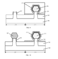
- FIG. 1 illustrates a schematic cross-section view of a Fin-FET fabricated by an existing method
- FIGS. 2-16 illustrate schematic views of semiconductor structures corresponding to certain stages of an exemplary fabrication method consistent with disclosed embodiments
- FIG. 17 illustrates variation of atom percentage concentration for Ge, Si, and B in the first epitaxial layer and the first covering layer along a direction from the top of the first covering layer to the bottom of the first epitaxial layer;
- FIG. 18 illustrates variation of atom percentage concentration for Ge, Si, and P in the second epitaxial layer and the second covering layer along a direction from the top of the second covering layer to the bottom of the second epitaxial layer;
- FIG. 19 illustrates a flowchart of the exemplary fabrication process consistent with disclosed embodiments.
- the epitaxial layer is often made of a semiconductor material and the conductive structure formed on the epitaxial layer is usually made of a metal. Therefore, the interface between the epitaxial layer and the conductive structure is a semiconductor/metal interface and, thus, a Schottky barrier may be formed at the interface between the epitaxial layer and the conductive structure. As a result, charge carriers may not be able to easily pass through the interface between the epitaxial layer and the conductive structure and, thus, the contact resistance between the epitaxial layer and the conductive structure may be large. Moreover, such a large contact resistance between the epitaxial layer and the conductive structure may affect the performance of the ultimately-formed semiconductor device.
- An existing method to reduce the contact resistance between the epitaxial layer and the conductive structure is to use a metal silicide to form an electric contact layer on the surface of a stress layer.
- the use of the metal silicide may reduce the contact resistance between the conductive structure and the stress layer.
- FIG. 1 shows a schematic cross-section view of a Fin-FET fabricated by an existing method.
- the Fin-FET includes a substrate 100 , a fin structure 101 formed on the surface of the substrate 100 , and an isolation layer 102 .
- the isolation layer 102 is formed to cover a portion of each side surface of the fin structure 101 .
- the top surface of the isolation layer 102 is lower than the top surface of the fin structure 101 .
- the Fin-FET further includes a gate structure 104 formed across the fin structure 101 .
- the gate structure 104 covers a portion of the side surface and the top surface of the fin structure 101 .
- the Fin-FET also includes an epitaxial layer 105 formed in the fin structure 101 on the two sides of the gate structure 104 and a covering layer 106 formed on the surface of the epitaxial layer 105 .
- the epitaxial layer 105 contains P-type ions or N-type ions.
- the covering layer 106 is then converted into an electric contact layer through a metal silicide process performed subsequently.
- the electric contact layer is made of a metal silicide material.
- the metal silicide process includes forming a metal layer on the surface of the covering layer 106 , and then performing an annealing process to allow the metal ions in the metal layer to diffuse into the covering layer 106 . After annealing, an electric contact layer is formed from the covering layer 106 . Finally, the metal silicide process further includes removing the remaining portion of the metal layer after the annealing process.
- the covering layer 106 is made of single crystalline silicon while the metal layer is made of Ni or Co.
- the electric contact layer is used to connect to a subsequently-formed conductive structure, such as a conductive plug, etc. By introducing the electric contact layer, the contact resistance between the conductive structure and the epitaxial layer 105 may be reduced and, thus, the performance of the Fin-FET is improved.
- the feature size of Fin-FETs also becomes smaller. Therefore, the contact area between the electric contact layer and the conductive structure may also be reduced, leading to an increase in the contact resistance between the conductive structure and the epitaxial layer 105 . As a result, the performance of Fin-FET may be degraded.
- one method is to reduce the height of the Schottky barrier between the electric contact layer and the epitaxial layer 105
- the other method is to increase the doping concentration of P-type ions or N-type ions at the interface between the electric contact layer and the epitaxial layer.
- introducing metal ions may cause Fermi level pinning in the semiconductor material. Therefore, after forming the electric contact layer using Ni or Co, further doping the semiconductor with P-type or N-type ions may not be able to effectively reduce the contact resistance between the electric contact layer and the epitaxial layer.
- FIG. 19 shows a flowchart of an exemplary process for fabricating a Fin-FET device consistent with disclosed embodiments.
- FIGS. 2-16 show schematic views of semiconductor structures corresponding to certain stages of the exemplary fabrication method.
- FIG. 19 at the beginning of the fabrication process, a substrate including a plurality of P-type regions and a plurality of N-type regions may be provided and a plurality of fin structures may be formed in each of the P-type regions and the N-type regions (S 101 ).
- FIG. 2 shows a schematic cross-section view of the semiconductor structure.
- a substrate 200 may be provided.
- a plurality of P-type regions 210 and a plurality of N-type regions 220 may be formed in the substrate 200 .
- a plurality of fin structures 201 may be formed on the surface of each of the P-type regions 210 and the N-type regions 220 .
- an isolation layer 202 may also be formed on the surface of the substrate 200 .
- the isolation layer 202 may cover a portion of the side surfaces of each fin structure 201 and the top surface of the isolation layer 202 may be lower than the top surfaces of the fin structures 201 .
- the structure shown in FIG. 2 includes only one P-type region 210 and one N-type region 220 .
- the number of the P-type regions 210 may be greater than one, while the number of the N-type regions 220 may also be greater than one.
- each of the P-type region and the N-type region only includes one fin structure 201 .
- the number of the fin structures 201 formed in each of the P-type regions 210 may be more than one and the number of the fin structures 201 formed in each of the N-type regions 220 may also be more than one.
- the P-type region 210 may be used to form a PMOS transistor while the N-type region 220 may be used to form an NMOS transistor. Further, the width of the fin structures 201 in the P-type region 210 and the N-type region 220 may be smaller than or equal to 20 nm.
- the substrate 200 and the fin structures 201 may be formed by a method including the following steps. First, a semiconductor base is provided. A mask layer may then be formed on the surface of the semiconductor base. The mask layer may cover the regions on the semiconductor base corresponding to the fin structures 201 to be formed. A plurality of trenches may be formed in the semiconductor base by etching the semiconductor base using the mask layer as an etch mask. Simultaneously with the formation of the plurality of trenches, a plurality of fin structures 201 may also be formed in the semiconductor base between neighboring trenches. The portion of the semiconductor base below the plurality of fin structures 201 and the plurality of the trenches may form the substrate 200 .
- the semiconductor base may be made of single crystal silicon, single crystal germanium, silicon germanium, and/or silicon carbide.
- the substrate 200 and the fin structures 201 are formed from single crystal silicon.
- the fin structures 201 may be formed by a method including the following steps. First, a substrate 200 is provided. A fin structure layer may then be formed on the surface of the substrate 200 by an epitaxial process. A mask layer may be formed on the surface of the fin structure layer with the mask layer covering the regions corresponding to the plurality of fin structures 201 to be formed. A plurality of trenches may be formed in the fin structure layer by etching the fin structure layer using the mask layer as an etch mask. Simultaneously with the formation of the plurality of trenches, a plurality of fin structures 201 may also be formed in the fin structure layer between neighboring trenches.
- the substrate 200 may be made of silicon, silicon germanium, silicon carbide, silicon on insulator (SOI), germanium on insulator (GOI), glass, or a Group III-V semiconductor material such as gallium nitride, gallium arsenide, etc.
- the fin structures 201 may be made of silicon, germanium, silicon carbide, and/or silicon germanium.
- the isolation layer 202 may be used to separate neighboring fin structures 201 .
- the isolation layer 202 may be made of one or more of SiO x , SiN x , SiON, a low-k dielectric material (e.g., a material with a dielectric constant greater than or equal to 2.5 but less than 3.9), and an ultra-low-k dielectric material (e.g., a material with a dielectric constant less than 2.5).
- the isolation layer 202 is made of SiO x .
- the thickness of the isolation layer 202 may be in a range of 50 nm to 80 nm. For example, the thickness of the isolation layer 202 may be 60 nm.
- the isolation layer 202 may be formed by a method including the following steps. First, an isolation film may be formed on the surfaces of the substrate 200 and the plurality of fin structures 201 . A planarization process may then be performed on the isolation film until the top surface of the fin structures 201 is exposed. After the planarization process, the isolation film may then be etched back to expose a portion of the side surfaces of each fin structure 201 . As such, the isolation layer 202 may be formed.
- a mask layer may be used for forming the plurality of fin structures 201 in a previous process. Accordingly, after forming the isolation layer 202 , the mask layer situated on the top surfaces of the fin structures 201 may be removed. The mask layer may serve as a stop layer during the planarization process performed on the isolation film. Therefore, the mask layer may be used to protect the top surface of the plurality of fin structures 201 .
- the fabrication method may further include forming a first well region in the substrate 200 and the fin structures 201 of the P-type region while a second well region in the substrate 200 and the fin structures 201 of the N-type region.
- the first well region and the second well region may be formed by an ion implantation process performed before or after the formation of the fin structures 201 .
- FIG. 3 shows a schematic view of the corresponding semiconductor structure.
- FIG. 4 shows a cross-section view of the semiconductor structure shown in FIG. 3 along a BB′ line.
- a gate structure 203 across each fin structure 201 in the P-type region 210 and the N-type region 220 may be formed.
- Each gate structure 203 (shown in FIG. 4 ) may be formed on a portion of the side and the top surfaces of the corresponding fin structure 201 .
- the gate structure 203 may include a gate dielectric layer formed on a portion of the isolation layer 202 and a portion of the side and the top surfaces of the corresponding fin structure 201 .
- the gate structure 203 may also include a gate electrode layer formed on the surface of a gate dielectric layer and sidewall spacers formed on the side surfaces of the gate electrode layer and the dielectric layer.
- the gate structure 203 may be a dummy gate structure.
- the dummy gate structure may be used to occupy a space for a subsequently-formed high-k metal gate (HKMG) structure. Therefore, the HKMG structure may be formed by a gate last process.
- the gate electrode layer may be made of polycrystalline silicon.
- the gate dielectric layer may be made of SiO x or a high-k dielectric material (e.g., a material with a dielectric constant greater than 3.9).
- the sidewall spacers (not labeled) may be made of one or more of SiO x , SiN X , SiON, etc.
- the gate electrode layer may be removed and a metal gate electrode may be formed.
- the gate dielectric layer is made of SiO x
- the gate dielectric layer may also be removed and a high-k dielectric layer may then be formed prior to the formation of the metal gate electrode.
- the gate structure 203 may be directly adopted in the ultimately-formed transistor.
- the gate electrode layer may be made of polycrystalline silicon
- the gate dielectric layer may be made of SiO x
- the sidewall spacers may be made of one or more of SiO x , SiN X , SiON, etc.
- the fabrication method may further include forming a lightly-doped region in the corresponding fin structure 201 on both sides of the gate structure 203 .
- the lightly-doped region in the P-type region 210 may be doped with P-type ions and the P-type ions may include boron ions or indium ions.
- the lightly-doped region in the N-type region 220 may be doped with N-type ions and the N-type ions may include phosphor ions or arsenic ions.
- a first epitaxial layer may be formed on the top of the fin structure 201 on both sides of the gate structure 203 in the P-type region 210 .
- the first epitaxial layer may be used to form the source region and the drain region of the ultimately-formed PMOS transistor.
- a first barrier layer may be formed on the surfaces of the isolation layer, the gate structure, and the fin structure in the N-type region and also on the side surfaces of the fin structure in the P-type region (S 103 ).
- FIG. 5 shows a schematic cross-section view of the corresponding semiconductor structure.
- a first barrier layer 204 may be formed. Specifically, in the N-type region 220 , the first barrier layer 204 may be formed on the surfaces of the isolation layer 202 and the gate structure 203 (referring to FIG. 4 ) as well as the side and the top surfaces of the fin structure 201 ; while in the P-type region 210 , the first barrier layer 204 may be formed on the side surfaces of the fin structure 201 . Therefore, the first barrier layer 204 may expose a portion of the top surface of the fin structure 201 on both sides of the gate structure 203 in the P-type region (referring to FIG. 4 ).
- the first barrier layer 204 may be used as a mask in a subsequent process to form a first epitaxial layer.
- the first barrier layer 204 may be made of a material including one or two of SiO x and SiON.
- the first barrier layer 204 may be formed by a method including the following steps. First, a first barrier film may be formed on the surfaces of the isolation layer 202 , the fin structures 201 , and the gate structures 203 . Further, a first patterned layer 208 may be formed to cover the surface of the N-type region 220 . An etch back process may then be performed on the first barrier film using the first patterned layer 208 as an etch mask until the surface of the isolation layer 202 and the top surfaces of the fin structure 201 and the gate structure 203 in the P-type region 210 are exposed. After performing the etch back process, the first barrier layer 204 may be formed.
- the first barrier film may be formed by chemical vapor deposition (CVD), physical vapor deposition (PVD), or atomic layer deposition (ALD).
- the etch back process may be an anisotropic dry etching process. Therefore, after the etch back process, the first barrier film may remain on the side surface of the fin structure 201 and the side surface of the gate structure 203 .
- the first patterned layer 208 may include a patterned photoresist layer.
- the first barrier layer 204 is made of SiN x . Further, prior to forming the first barrier film, the fabrication method may also include forming a silicon oxide layer on the surface of the exposed portion of the fin structure 201 .
- the first barrier layer may be formed on the surface of the silicon oxide layer.
- the silicon oxide layer may be formed by an oxidation process, such as an in-situ steam generation (ISSG) process, etc.
- a first opening may be formed in the fin structure 201 of the P-type region 220 on each side of the gate structure 203 .
- a first opening may be formed in the fin structure 201 on each side of the gate structure 203 by etching the top of the fin structure 201 in the P-type region using the first barrier layer 204 as an etch mask.
- a first epitaxial layer may be formed to fill each first opening.
- the bottom of the first epitaxial layer may be lower than the top surface of the fin structure 201 .
- the first epitaxial layer may induce a stress into the channel region under the gate structure 203 .
- the first opening may be formed by a process including an anisotropic dry etching process.
- the first opening may be formed by a method including the following steps. First, an initial opening may be formed by performing an anisotropic dry etching process to etch the corresponding fin structure 201 . Further, an anisotropic wet etching process may be performed to etch the initial opening. After the anisotropic wet etching process, the sidewall of the initial opening and the surface of the fin structure 201 may form a vertex angle and the vertex angle may extend into the fin structure 201 on the bottom of the gate structure 203 , forming a first opening. The sidewall of the first opening and the bottom surface of the fin structure 201 may form a ⁇ shape. Therefore, the first opening may be a ⁇ -type opening.
- a first epitaxial layer may be formed on the top surface of the fin structure in the P-type region using the first barrier layer as a mask (S 104 ).
- FIG. 6 shows a schematic view of the corresponding semiconductor structure.
- FIG. 7 shows a cross-section view of the semiconductor structure shown in FIG. 6 along a CC′ line.
- a first epitaxial layer 211 may be formed on the top surface of the fin structure 201 in the P-type region 210 on both sides of the gate structure 201 .
- the first epitaxial layer may be formed by a selective epitaxial deposition process using the first barrier layer 204 as a mask. Therefore, the first epitaxial layer may fill up both first openings on the two sides of the gate structure 203 in the P-type region 210 .
- the P-type region may be used to form a PMOS transistor. Therefore, in one embodiment, the first epitaxial layer 211 may be made of SiGe and may be doped with P-type ions. The first epitaxial layer 211 may be formed on the top of the fin structure 201 on both sides of the gate structure 230 so that the first epitaxial layer 211 may form a source region and a drain region for the ultimately-formed PMOS transistor. The first epitaxial layer 211 may induce a compressive stress into the channel region under the gate structure 203 and, thus, the mobility of charge carriers in the ultimately-formed PMOS transistor may be improved.
- the first epitaxial layer 211 may be formed by a selective epitaxial deposition process.
- the deposition parameters for the selective epitaxial deposition process may include a deposition temperature in a range of 500° C. to 800° C., a deposition pressure in a range of 1 Torr to 100 Torr, and a process gas including a silicon-containing gas (such as SiH 4 , SiH 2 Cl 2 , etc.) and a germanium-containing gas (such as GeH 4 , etc.).
- the flowrate of the silicon-containing gas and the germanium-containing gas may be in a range of 1 sccm to 1000 sccm.
- the process gas may further include HCl and H 2 .
- the flowrate of HCl may be in a range of 1 sccm to 1000 sccm and the flowrate of H 2 may be in a range of 0.1 sccm to 50 sccm.
- the atomic percentage concentration of the germanium atoms in the first epitaxial layer 211 may gradually increase from a certain value to a first concentration and then gradually decrease to a second concentration.
- the first concentration may be 50% while the second concentration may be 5%.
- the first concentration may be the highest atomic percentage concentration for germanium ions in the first epitaxial layer 211 .
- a higher atomic percentage concentration of the germanium ions in the first epitaxial layer 211 may correspond to a larger mismatch in lattice constant between the first epitaxial layer 211 and the fin structure 201 . Therefore, the first epitaxial layer 211 may induce a compressive stress into the channel region so that the performance of the ultimately-formed PMOS transistor may be desired.
- the atomic percentage concentration of germanium atoms may gradually reach the highest value (e.g., the first concentration) in the formed first epitaxial layer 211 , and may then gradually decrease until reaching the second concentration of 5%. Therefore, at the surface of the first epitaxial layer 211 , the atomic percentage concentration of germanium atoms may be low, while the atomic percentage concentration of silicon atoms may be high.
- P-type ions may be introduced into the first epitaxial layer 211 using an in-situ doping method.
- the P-type ions doped into the first epitaxial layer 211 may be boron ions.
- the doping concentration of the boron ions in the first epitaxial layer 211 may be smaller than or equal to 1E21 atoms/cm 3 .
- the doping concentration of boron ions may gradually increase to 1E21 atoms/cm 3 . Therefore, the highest doping concentration in the first epitaxial layer 211 may be 1E21 atoms/cm 3 .
- a first covering layer may be formed on the surface of the first epitaxial layer 211 , and then a first metal silicide layer may be formed from the first covering layer.
- the doping concentration of boron ions may be high at the surface of the first epitaxial layer 211 , after forming the first metal silicide layer, the doping concentration of boron ions at the interface between the first metal silicide layer and the first epitaxial layer 211 may also be high. Such a high boron concentration at the interface between the first metal silicide layer and the first epitaxial layer 211 may help reduce the contact resistance between the first epitaxial layer 211 and the first metal silicide layer.
- a first covering layer may be formed on the surface of the first epitaxial layer (S 105 ).
- FIG. 8 shows a schematic cross-section view of the corresponding semiconductor structure.
- a first covering layer 212 may be formed on the surface of the first epitaxial layer 211 .
- the first covering layer 212 may be made of SiGe and may be doped with P-type ions.
- the first covering layer 212 may also be made of any other appropriate semiconductor material doped with P-type ions.
- the first covering layer 212 may be used to form a first metal silicide layer on the first epitaxial layer 211 .
- the first metal silicide layer may be used to reduce the contact resistance between the first epitaxial layer 211 and a subsequently-formed first contact plug.
- the first covering layer 212 may be made of SiGe.
- the first covering layer 212 may be formed by a selective epitaxial deposition process.
- the atomic percentage concentration of germanium ions in the first covering layer 212 may be in a range of 45% to 55%.
- the atomic percentage concentration of germanium ions in the first covering layer 212 may be the first concentration. That is, the atomic percentage concentration of germanium ions in the first covering layer 212 may be 50%. In other embodiments, the atomic percentage concentration of germanium ions in the first covering layer 212 may be greater than the first concentration.
- the germanium concentration in the first covering layer 212 may be high so that after forming a silicide layer containing titanium ions on the surface of the first covering layer 212 , titanium ions in the silicide layer may react with germanium ions in the first covering layer 212 to form a titanium-silicon compound, such as a titanium-silicon-germanium compound.
- the height of the Schottky barrier between titanium-silicon and the P-type semiconductor may be low. Specifically, the height of the Schottky barrier between titanium-silicon and the P-type semiconductor may be lower than the height of a Schottky barrier between the P-type semiconductor and a nickel-silicon compound or a cobalt-silicon compound. Therefore, the contact resistance between the first covering layer 212 and the first epitaxial layer 211 may be reduced.
- the first epitaxial layer 211 may be made of SiGe doped with boron ions, the height of the Schottky barrier between SiGe and titanium-silicon may be lower than the height of the Schottky barrier between Si and titanium-silicon. Therefore, the contact resistance between the first covering layer and the first epitaxial layer 211 may be reduced.
- the P-type ions doped into the first covering layer 212 may be boron ions. Further, during the selective epitaxial deposition process to form the first covering layer 212 , the P-type ions may be introduced into the first covering layer 212 using an in-situ doping process.
- the doping concentration of boron ions in the first covering layer 212 may be higher than the doping concentration of boron ions in the first epitaxial layer 211 .
- the doping concentration of boron ions in the first covering layer 212 may be in a range of 1E21 atoms/cm 3 to 1E22 atoms/cm 3 . In one embodiment, the doping concentration of boron ions in the first covering layer 212 may be 1E22 atoms/cm 3 .
- the doping concentration of boron ions in the first covering layer 212 may be high so that after forming the first metal silicide layer using the first covering layer 212 , the concentration of boron ions in the first metal silicide layer may also be high. Such a high boron concentration in the first metal silicide layer may further reduce the contact resistance between the first metal silicide layer and the first epitaxial layer 211 .
- FIG. 17 shows variation of atom percentage concentration for Ge, Si, and B in the first epitaxial layer and the first covering layer along a direction from the top of the first covering layer 212 to the bottom of the first epitaxial layer 211 .
- a second epitaxial layer may be formed on the top of the fin structure 201 on both sides of the fin structure 201 in the N-type region 220 .
- a second barrier layer may be formed on the surfaces of the isolation layer, the gate structure, and the fin structure in the P-type region and also on the side surfaces of the fin structure in the N-type region (S 106 ).
- FIG. 9 shows a schematic cross-section view of the corresponding semiconductor structure.
- a second barrier layer 205 may be formed. Specifically, in the P-type region 210 , the second barrier layer 205 may be formed on the surfaces of the isolation layer 202 and the gate structure 203 (referring to FIG. 4 ) as well as the side and the top surfaces of the fin structure 201 ; while in the N-type region 220 , the second barrier layer 205 may be formed on the side surfaces of the fin structure 201 . Therefore, the second barrier layer 205 may expose a portion of the top surface of the fin structure 201 on both sides of the gate structure 203 (referring to FIG. 4 ) in the N-type region 220 .
- the fabrication process may also include removing the first barrier layer 204 formed on the isolation layer 202 after forming the first covering layer 212 . In other embodiments, after forming the first covering layer 212 , the first barrier layer 204 may not be removed.
- the second barrier layer 205 may expose a portion of the top surface of the fin structure 201 on both sides of the gate structure 203 in the N-type region.
- the second barrier layer 205 may be used as a mask in a subsequent process to form a second epitaxial layer.
- the second barrier layer 205 may be made of one or two of SiN, SiON, etc.
- the second barrier layer may be formed by a process including the following steps. First, a second barrier film may be formed on the isolation layer 202 , the fin structure 201 , the gate structure 203 , and the first covering layer 212 . Further, a second patterned layer may be formed on the surface of the portion of the second barrier film formed in the P-type region 210 . Finally, a second barrier layer 205 may then be formed by performing an etch back process on the second barrier film using the second patterned layer as an etch mask until the surface of the isolation layer 202 , the top surface of the fin structure 201 , and the top surface of the gate structure in the N-type region 220 are exposed.
- the second barrier film may be formed by a process including chemical vapor deposition (CVD), physical vapor deposition (PVD), atomic layer deposition (ALD), etc.
- the etch back process may be an anisotropic dry etching process. After performing the anisotropic dry etching process, the second barrier layer formed on the sidewall surfaces of the gate structure 203 and the fin structure 201 may be retained. Further, the second patterned layer may include a patterned photoresist layer.
- the second barrier layer 205 may be made of SiN.
- the fabrication process may further include forming a SiO x layer on the exposed portion of the fin structure 201 .
- the second barrier film may then be formed on the surface of the SiO x layer.
- the SiO x layer may be formed by an oxidation process, such as an ISSG process.
- the second barrier layer 205 on the side surfaces of the fin structure 201 in the N-type region 220 may be formed from the portion of the first barrier film formed in the N-type region 220 .
- an etch back process may be performed on the portion of the first barrier film in the N-type region 220 until the surfaces of the isolation layer 202 , the top surface of the fin structure 201 , and the top surface of the gate structure 203 in the N-type region 220 are exposed.
- the remaining portion of the first barrier film on the side surfaces of the fin structure 201 in the N-type region may become the second barrier layer 205 .
- the second barrier layer 205 in the N-type region 220 may be formed simultaneously with the first barrier layer 204 in the P-type region 210 in one etch back process.
- the second barrier layer 205 in the N-type region 220 may also be formed by an etch back process different from the etch back process for forming the first barrier layer 204 in the P-type region 210 .
- a second opening may be formed in the fin structure 201 on each side of the gate structure 203 in the N-type region 220 by etching the top of the fin structure 201 in the N-type region 220 using the second barrier layer 205 as an etch mask.
- a second epitaxial layer may be formed in both second openings. The bottom of the second epitaxial layer may be lower than the top surface of the fin structure 201 . The second epitaxial layer may induce a stress into the channel region under the gate structure 203 .
- the second opening may be formed by a process including an anisotropic dry etching process.
- the depth of the second openings may be smaller than the depth of the first openings. Therefore, the bottom of the second epitaxial layer formed subsequently in the second openings may be above the bottom of the first epitaxial layer 211 formed in the first openings.
- a second epitaxial layer may be formed on the top surface of the fin structure in the N-type region using the second barrier layer as a mask (S 107 ).
- FIG. 10 shows a schematic cross-section view of the corresponding semiconductor structure.
- a second epitaxial layer 221 may be formed on the top surface of the fin structure 201 in the N-type region 220 on both sides of the gate structure 201 .
- the second epitaxial layer may be formed by a selective epitaxial deposition process using the second barrier layer 205 as a mask. Therefore, the second epitaxial layer may fill up both second openings on the two sides of the gate structure 203 in the N-type region 220 .
- the N-type region 220 may be used to further form an NMOS transistor. Therefore, in one embodiment, the second epitaxial layer 221 may be made of SiP. The second epitaxial layer 221 may be formed on the top of the fin structure 201 on both sides of the gate structure 230 so that the second epitaxial layer 221 may form the source region and the drain region for the ultimately-formed NMOS transistor.
- the concentration of the phosphor ions in the second epitaxial layer 221 may be high. Therefore, SiP in the second epitaxial layer 221 may form a zinc blende structure.
- the lattice constant of SiP in the zinc blende structure may be smaller than the lattice constant of single crystalline silicon. Therefore, the formed second epitaxial layer 221 may induce a tensile stress into the channel region under the gate structure 203 and, thus, the mobility of charge carriers in the ultimately-formed NMOS transistor may be improved.
- the depth of the second openings may be smaller than the depth of the first openings. Because the growth rate of SiP may be large, the presence of the second openings may help suppress the rapid growth of SiP and, thus, avoid forming a bridge connection between neighboring fin structure and the second epitaxial layer 221 . Therefore, forming the second openings may ensure desired morphology for the ultimately-formed second epitaxial layer 221 .
- the second epitaxial layer 221 may be formed by a selective epitaxial deposition process.
- the selective epitaxial deposition process for forming the second epitaxial layer 221 may use process parameters including a process temperature in a range of 500° C. to 800° C. and a process pressure in a range of 1 Torr to 100 Torr.
- the process gas in the selective epitaxial deposition process may include a silicon-containing gas (such as SiH 4 , SiH 3 C 12 , etc.).
- the flowrate of the silicon-containing gas may be in a range of 1 sccm to 1000 sccm.
- the process gas of the selective epitaxial deposition process may also include HCl and H 2 .
- the flowrate of HCl may be in a range of 1 sccm to 1000 sccm while the flowrate of H 2 may be in a range of 100 sccm to 50000 sccm.
- phosphor ions may be introduced into the second epitaxial layer 221 using an in-situ doping method.
- the doping concentration of phosphor ions in the second epitaxial layer 221 may be smaller than or equal to 1E21 atoms/cm 3 .
- the doping concentration of the phosphor ions may gradually increase from a certain value to 1E21 atoms/cm 3 . Therefore, at the surface of the second epitaxial layer 221 , the doping concentration of phosphor ions may reach the highest value, i.e. 1E21 atoms/cm 3 .
- a second covering layer may be formed on the surface of the second epitaxial layer 221 , and then a second metal silicide layer may be formed from the second covering layer.
- the doping concentration of phosphor ions may be high at the surface of the second epitaxial layer 221 , after forming the second metal silicide layer, the doping concentration of phosphor ions at the interface between the second metal silicide layer and the second epitaxial layer 221 may also be high. Such a high phosphor concentration at the interface between the second metal silicide layer and the second epitaxial layer 221 may help reduce the contact resistance between the second epitaxial layer 221 and the second metal silicide layer.
- FIG. 11 shows a schematic cross-section view of the corresponding semiconductor structure.
- a second covering layer 222 may be formed on the surface of the second epitaxial layer 221 .
- the second covering layer 222 may be made of SiGe and may be doped with N-type ions.
- the second covering layer 222 may be made of any other appropriate semiconductor material doped with N-type ions.
- the second covering layer 222 may be used to form a second metal silicide layer on the second epitaxial layer 221 .
- the second metal silicide layer may be used to reduce the contact resistance between the second epitaxial layer 221 and a subsequently-formed second contact plug.
- the second covering layer 222 may be made of SiGe.
- the second covering layer 222 may be formed by a selective epitaxial deposition process.
- the atomic percentage concentration of germanium ions in the second covering layer 222 may be in a range of 45% to 55%.
- the atomic percentage concentration of germanium ions in the second covering layer 222 may be the same as the atomic percentage concentration of germanium ions in the first covering layer 212 . That is, the atomic percentage concentration of germanium ions in the second covering layer 222 may also be the first concentration, i.e. 50%. In other embodiments, the atomic percentage concentration of germanium ions in the second covering layer 222 may be greater than the first concentration.
- both the first covering layer 212 and the second covering layer 222 may be made of SiGe and the atomic concentrations of germanium ions in the first covering layer 212 and the second covering layer 222 are the same. Therefore, during a subsequently-performed first annealing process, the silicification rate for the first covering layer 212 may also be the same as the silicification rate for the second covering layer 222 . Moreover, because the thickness of the first covering layer 212 may be the same as the thickness of the second covering layer 222 , the resistivity of the first covering layer 212 may also be the same as the resistivity of the second covering layer 222 . Therefore, the electrical performance of the ultimately-formed PMOS transistor and NMOS transistor may be more stable.
- the N-type ions doped into the second covering layer 222 may be phosphor ions. Further, during the selective epitaxial deposition process to form the second covering layer 222 , the N-type ions may be introduced into the second covering layer 222 using an in-situ doping process.
- the doping concentration of phosphor ions in the second covering layer 222 may be higher than the doping concentration of phosphor ions in the second epitaxial layer 221 .
- the doping concentration of phosphor ions in the second covering layer 222 may be in a range of 1E21 atoms/cm 3 to 1E22 atoms/cm 3 . In one embodiment, the doping concentration of phosphor ions in the second covering layer 222 may be 1E22 atoms/cm 3 .
- the doping concentration of phosphor ions in the second covering layer 222 may be high so that after forming the second metal silicide layer from the second covering layer 222 in a subsequent process, the concentration of phosphor ions in the second metal silicide layer may also be high. Such a high phosphor concentration in the second metal silicide layer may further reduce the contact resistance between the second metal silicide layer and the second epitaxial layer 221 .
- FIG. 18 shows variation of atom percentage concentration for Ge, Si, and P in the second epitaxial layer and the second covering layer along a direction from the top of the second covering layer 222 to the bottom of the second epitaxial layer 221 .
- a silicide layer may be formed on at least a portion of the surface of the first covering layer 212 and also on at least a portion of the second covering layer 222 .
- the silicide layer may include titanium ions.
- a dielectric layer may be formed on the surfaces of the isolation layer, the gate structures, and the fin structures with a first via exposing the first covering layer and a second via exposing the second covering layer (S 109 ).
- FIG. 12 shows a schematic cross-section view of the corresponding semiconductor structure.
- a dielectric layer 206 may be formed on the isolation layer 202 , the gate structures 203 (referring to FIG. 4 ), and the fin structures 201 in both the N-type region and the P-type region.
- a first via 213 may be formed in the dielectric layer 206 to expose the first covering layer 212 while a second via 223 may be formed in the dielectric layer 206 to expose the second covering layer 222 .
- the portion of the second barrier layer 205 formed on the surface of the isolation layer 202 may be removed.
- the dielectric layer 206 may be formed by a method including the following steps. First a dielectric film may be formed on the surfaces of the isolation layer 202 , the fin structures 201 , the first covering layer 212 , the second covering layer 222 , and the gate structures 203 (referring to FIG. 4 ). A planarization process may then be performed on the dielectric film to form the dielectric layer. A third patterned layer may be formed on the surface of the dielectric layer 206 . The third patterned layer may expose a portion of the surface of the dielectric layer 206 corresponding to the positions of the subsequently-formed first via 213 and the subsequently-formed second via 223 . Further, the first via 213 and the second via 223 may be formed by etching the dielectric layer 206 using the third patterned layer as an etch mask until the first covering layer 212 and the second covering layer 222 are exposed.
- the dielectric film may be formed by a process including CVD, PVD, ALD, etc.
- the CVD process may include flowable chemical vapor deposition (FCVD), plasma enhanced chemical vapor deposition (PECVD), and high aspect ratio chemical vapor deposition process (HARP).
- the planarization process may be a chemical mechanical polishing process.
- the process to etch the dielectric layer 206 may be an anisotropic dry etching process.
- the third patterned layer may include a patterned photoresist layer.
- the dielectric layer 206 may be made of SiO x , SiN x , SiON, a low-k dielectric material (e.g., a material with a dielectric constant greater than or equal to 2.5, but less than 3.9, such as porous SiO x and porous SiN x ), or an ultra-low-k dielectric material (e.g., a material with a dielectric constant less than 2.5, such as porous SiCOH).
- a low-k dielectric material e.g., a material with a dielectric constant greater than or equal to 2.5, but less than 3.9, such as porous SiO x and porous SiN x
- an ultra-low-k dielectric material e.g., a material with a dielectric constant less than 2.5, such as porous SiCOH.
- the gate structures 203 may be dummy gate structures.
- the dielectric layer 206 may further include a first sub-dielectric layer and a second sub-dielectric layer.
- the first sub-dielectric layer may be formed on the surfaces of the isolation layer 202 , the fin structures 201 , the first covering layer 212 , and the second covering layer 222 .
- the second sub-dielectric layer may be formed on the surfaces of the first sub-dielectric layer and the gate structures 203 .
- the surface of the first sub-dielectric layer may be leveled with the top surface of the gate structures 203 .
- the first sub-dielectric layer may be formed by a process including the following steps. First, a first sub-dielectric film may be formed on the surfaces of the substrate and the gate structures 203 . A first sub-dielectric layer may then be formed by performing a planarization process on the first sub-dielectric film until the top surface of the gate structures 203 is exposed. The first sub-dielectric layer may be used as a mask during a subsequent process to remove the dummy gate electrode in each gate structure 203 and then form a HKMG. After removing the dummy gate electrode in each gate structure and forming the corresponding HKMG, the second sub-dielectric layer may then be formed by a process including CVD, PVD, ALD, etc.
- the dummy gate electrode in each gate structure 203 may be removed to form a gate electrode opening. Further, a high-k dielectric layer may be formed on the inner surface of the sidewalls of the gate electrode opening. Finally, a metal gate electrode may be formed on the high-k dielectric layer by filling up the gate electrode opening. As such a HKMG is formed.
- the gate structure 203 may be a dummy gate structure with a high-k dielectric layer formed between the corresponding fin structure 201 and the dummy gate electrode. Accordingly, after forming the first sub-dielectric layer and removing the dummy gate electrode, a metal gate electrode may be directly formed on the high-k dielectric layer to complete a HKMG.
- an ion implantation process may be performed on the first covering layer through the first via to introduce P-type doping ions into the first covering layer (S 110 ).
- FIG. 13 shows a schematic diagram of performing the ion implantation process on the first covering layer.
- a mask layer (not labeled) may be formed to cover the N-type region 220 .
- An ion implantation process may then be performed to introduce ions into the first covering layer 212 exposed on the bottom of the first via 213 .
- P-type ions may be implanted into the surface of the first covering layer 212 to reduce the contact resistance between the first covering layer 212 and a subsequently-formed first contact plug.
- the mask layer may then be removed after the ion implantation process.
- the P-type ions implanted into the first covering layer 212 on the bottom of the first via 213 may be boron ions.
- the P-type ions may be implanted into the first covering layer 212 along a direction perpendicular to the surface of the substrate 200 .
- an ion implantation process may be performed on the second covering layer through the second via to introduce N-type doping ions into the second covering layer (S 111 ).
- FIG. 14 shows a schematic diagram of performing the ion implantation process on the second covering layer.
- a mask layer (not labeled) may be formed to cover the P-type region 210 .
- An ion implantation process may then be performed to introduce ions into the second covering layer 222 exposed on the bottom of the second via 223 .
- N-type ions may be implanted into the surface of the second covering layer 222 to reduce the contact resistance between the second covering layer 222 and a subsequently-formed second contact plug.
- the mask layer may then be removed after the ion implantation process.
- the N-type ions implanted into the second covering layer 222 on the bottom of the second via 223 may be phosphor ions.
- the N-type ions may be implanted into the second covering layer 222 along a direction perpendicular to the surface of the substrate 200 .
- a second annealing process may be performed to active the P-type ions in the first covering layer 212 and the first epitaxial layer 211 as well as the N-type ions in the second covering layer 222 and the second epitaxial layer 221 .
- the second annealing process may be a spike annealing process or a laser annealing process.
- a silicification layer may be formed on the surface of the first covering layer on the bottom of the first via and also on the surface of the second covering layer on the bottom of the second via (S 112 ).
- FIG. 15 shows a schematic cross-section view of the corresponding semiconductor structure.
- a silicification layer 207 may be formed on the surface of the first covering layer 212 on the bottom of the first via 213 and also on the surface of the second covering layer 222 on the bottom of the second via 223 .
- the silicification layer 207 may be a metal layer containing titanium ions.
- the silicification layer 207 may be formed by a process including CVD, PVD, ALD, etc. In one embodiment, the silicification layer 207 may be formed by an ALD process.
- the thickness of the silicification layer 207 made of titanium silicide, may be in a range of 10 nm to 50 nm.
- the silicification layer 207 may also be formed on the surface of the dielectric layer 206 , the sidewall surface of the first via 213 , and the sidewall surface of the second via 223 .
- a portion of the first covering layer 212 in contact with the silicification layer 207 may react with the silicification layer 207 and, thus, form a first metal silicide layer.
- a portion of the second covering layer 222 in contact with the silicification layer 207 may react with silicification layer 207 and, thus, form a second metal silicide layer.
- a first annealing process may be performed to let titanium ions diffuse into the first covering layer and the second covering layer and thus form a first metal silicide layer from the first covering layer and a second metal silicide layer from the second covering layer (S 113 ).
- FIG. 16 shows a schematic cross-section view of the corresponding semiconductor structure.
- a first annealing process may be performed.
- the titanium ions in the silicification layer 207 may diffuse into the first covering layer 212 and the second covering layer 222 , resulting in forming a first metal silicide layer 214 in the first covering layer 212 and a second silicide layer 224 in the second covering layer 222 .
- the first annealing process may be a flash annealing process.
- the process parameters used in the first annealing process may include a process temperature in a range of 750° C. to 950° C., a process time in a range of 10 ms to 500 ms, and a process gas including N 2 or an inert gas such as Ar or He.
- the first annealing process is performed at 800° C.
- the silicification layer 207 may be in contact with the first covering layer 212 and the second covering layer 222 , and may contain titanium ions. Therefore, during the first annealing process, the titanium ions may diffuse into the first covering layer 212 and the second covering layer 222 to form the first metal silicide layer 214 and the second metal silicide layer 224 .
- the first metal silicide layer 214 and the second metal silicide layer 224 may be made of TiSiGe.
- the first covering layer 212 may contain a high level of doped boron ions
- the first metal silicide layer 214 formed in the first covering layer 212 may also contain a high level of doped boron ions.
- the second covering layer 222 may contain a high level of doped phosphor ions
- the second metal silicide layer 224 formed in the second covering layer 222 may also contain a high level of doped phosphor ions.
- the first epitaxial layer 211 may be made of SiGe and the first metal silicide layer 214 may be made of TiSiGe, the height of the Schottky barrier between the first epitaxial layer 211 and the first metal silicide layer 214 may be small. Therefore, the contact resistance between the first epitaxial layer 211 and the first metal silicide layer 214 may also be small.
- the first metal silicide layer 214 may contain a high level of doped boron ions and the high doping concentration of boron ions may further reduce the height of Schottky barrier between the first epitaxial layer 211 and the first metal silicide layer 214 . Therefore, the contact resistance between the first epitaxial layer 211 and the first metal silicide layer 214 may be further reduced.
- the second epitaxial layer 221 may be made of SiP, while the second metal silicide layer 224 may be made of a phosphor-doped TiSiGe compound, i.e. a material containing titanium-silicon-phosphor.
- concentration of phosphor ions at the surface of the second epitaxial layer 221 may be high, which may help reduce the contact resistance between the second epitaxial layer 221 and the second metal silicide layer 224 .
- the second metal silicide layer 224 may contain a high level of doped phosphor ions and the high doping concentration of phosphor ions may further reduce the height of Schottky barrier between the second epitaxial layer 221 and the second metal silicide layer 224 . Therefore, the contact resistance between the second epitaxial layer 221 and the second metal silicide layer 224 may be further reduced.
- the first via 213 (referring to FIG. 15 ) and the second via 223 (referring to FIG. 15 ) may be filled with a conductive material to form a first contact plug 215 in the first via 213 and a second contact plug 225 in the second via 223 .
- the conductive material may include Cu, W, and Al.
- the first contact plug 215 and the second contact plug 225 may be formed by a process including the following steps. First, a conductive film may be formed on the surface of the dielectric layer 208 and also in the first via 213 and the second via 223 . A planarization process may then be performed on the conductive film until the surface of the dielectric layer 206 is exposed. As such, the first contact plug 215 may be formed in the first via 213 and the second contact plug 225 may be formed in the second via 223 .
- the conductive material may be formed by a process including CVD, PVD, electroplating, and chemical plating.
- the planarization process may be a chemical mechanical polishing process.
- the silicification layer 207 may not be removed prior to forming the first contact plug 215 and the second contact plug 225 .
- the silicification layer 207 may serve as a barrier layer between the first contact plug 215 and the dielectric layer 206 and also between the second contact plug 225 and the dielectric layer 206 . In other embodiments, the silicification layer 207 may be removed prior to forming the first contact plug 215 and the second contact plug 225 .
- FIG. 16 shows an exemplary semiconductor structure consistent with the disclosed embodiments.
- the Fin-FET device may include a substrate 200 with a plurality of P-type regions 210 and a plurality of N-type regions 220 . Further, each of the P-type region 210 and the N-type region 220 may include a plurality of fin structures 210 formed on the substrate 200 .
- the semiconductor structure shown in FIG. 16 is described to have one P-type region 210 and one N-type region 220 with each including one fin structure 210 .
- the width of each fin structure 210 may be smaller than or equal to 20 nm. In other embodiments, the number of P-type regions 210 and the number of N-type regions may be greater than one, while the number of fin structures formed on each P-type region 210 or on each N-type region 220 may also be greater than one.
- the Fin-FET device may include an isolation layer 202 formed on the surface of the substrate between neighboring fin structures 201 .
- the isolation layer 202 may cover a bottom portion of the side surfaces of each fin structure 201 .
- the top surface of the isolation layer 202 may be lower than the top surface of the fin structures 201 .
- the thickness of the isolation layer 202 may be in a range of 50 nm to 80 nm.
- the Fin-FET device may also include a gate structure (not shown) formed on the top surface of each fin structure 201 .
- the gate structure may be a HKMG.
- the sidewall surface of each fin structure 201 may be covered by a barrier layer.
- a first barrier layer 204 may cover the sidewall surfaces of the fin structure 201 in the P-type region while a second barrier layer 205 may cover the sidewall surfaces of the fin structure 201 in the N-type region.
- the first barrier layer 204 and the second barrier layer 205 may or may not be formed from a same barrier film.
- the Fin-FET device may further include a first epitaxial layer 211 formed on the top surface of the fin structure 201 in the P-type region and on both sides of the gate structure (not shown).
- the bottom of the first epitaxial layer 211 may be lower than the top surface of the fin structure 201 .
- the cross section of the first epitaxial layer 211 may have an/shape.
- the first epitaxial layer 211 may be made of SiGe and doped with P-type ions. Specifically, along a direction from the bottom to the top of the first epitaxial layer 211 , the atomic percentage concentration of the germanium atoms in the first epitaxial layer 211 may gradually increase from a certain value to a first concentration and then gradually decrease to a second concentration.
- the first concentration may be 50% while the second concentration may be 5%.
- the first concentration may be the highest atomic percentage concentration for germanium ions in the first epitaxial layer 211 .
- the doped P-type ions in the first epitaxial layer 211 may be boron ions.
- the doping concentration of the P-type ions in the first epitaxial layer 211 may be lower than or equal to 1E21 atoms/cm 3 .
- the Fin-FET device may also include a second epitaxial layer 221 formed on the top surface of the fin structure 201 in the N-type region and on both sides of the gate structure (not shown).
- the bottom of the second epitaxial layer 221 may be lower than the top surface of the fin structure 201 .
- the cross section of the second epitaxial layer 221 may have an/shape.
- the second epitaxial layer 221 may be made of SiP. Specifically, along a direction from the bottom to the top of the second epitaxial layer 221 , the atomic percentage concentration of the phosphor atoms in the second epitaxial layer 221 may gradually increase from a certain value to a highest concentration of 1E21 atoms/cm 3 . That is, the doping concentration of phosphor ions in the second epitaxial layer 221 may be smaller than or equal to 1E21 atoms/cm 3 .
- the Fin-FET device may further include a first covering layer 212 formed on the surface of the first epitaxial layer 211 in the P-type region, a second covering layer 222 formed on the surface of the second epitaxial layer 221 in the N-type region, and a silicification layer 207 formed over the first covering layer 212 and the second covering layer 222 .
- the silicification layer 207 may contain titanium ions.
- the Fin-FET device may include a first metal silicide layer 214 formed from a top portion of the first covering layer 212 in the P-type region and a second metal silicide layer 224 formed from a top portion of the second covering layer 222 in the N-type region.
- the first metal silicide layer 214 and the second metal silicide layer 224 may be simultaneously formed by performing a first annealing process to let the titanium ions in the silicification layer 207 diffuse into the top portion of the first covering layer 212 and the top portion of the second covering layer 222 , respectively.
- the first covering layer 212 may contain a high level of doped boron ions
- the first metal silicide layer 214 formed in the first covering layer 212 may also contain a high level of doped boron ions.
- the second covering layer 222 may contain a high level of doped phosphor ions
- the second metal silicide layer 224 formed in the second covering layer 222 may also contain a high level of doped phosphor ions.
- the Fin-FET device may also include a first contact plug 215 formed over the first metal silicide layer 214 , a second contact plug 225 formed over the second metal silicide layer 224 , and a dielectric layer 206 formed on the surfaces of the isolation layer 202 .
- the top surfaces of the dielectric layer 206 , the first contact plug 215 , and the second contact plug may be leveled with each other.
- the first epitaxial layer 211 may be made of SiGe and the first metal silicide layer 214 may be made of TiSiGe, the height of the Schottky barrier between the first epitaxial layer 211 and the first metal silicide layer 214 may be small. Therefore, the contact resistance between the first epitaxial layer 211 and the first metal silicide layer 214 may also be small.
- the first metal silicide layer 214 may contain a high level of doped boron ions and the high doping concentration of boron ions may further reduce the height of Schottky barrier between the first epitaxial layer 211 and the first metal silicide layer 214 . Therefore, the contact resistance between the first epitaxial layer 211 and the first metal silicide layer 214 may be further reduced.
- the second epitaxial layer 221 may be made of SiP, while the second metal silicide layer 224 may be made of a phosphor-doped TiSiGe compound, i.e. a material containing titanium-silicon-phosphor.
- concentration of phosphor ions at the surface of the second epitaxial layer 221 may be high, which may help reduce the contact resistance between the second epitaxial layer 221 and the second metal silicide layer 224 .
- the second metal silicide layer 224 may contain a high level of doped phosphor ions and the high doping concentration of phosphor ions may further reduce the height of Schottky barrier between the second epitaxial layer 221 and the second metal silicide layer 224 . Therefore, the contact resistance between the second epitaxial layer 221 and the second metal silicide layer 224 may be further reduced.
- the disclosed Fin-FET device and fabrication method may demonstrate several advantages in reducing the contact resistance in the formed Fin-FET devices.
- the P-type region is used to form a PMOS transistor while the N-type region is used to form an NMOS transistor.
- the first covering layer formed on the surface of the first epitaxial layer contains germanium ions, while the silicification layer subsequently-formed on the surface of the first covering layer contains titanium ions. Therefore, after performing the first annealing process, the first metal silicide layer formed from the top portion of the first covering layer is made of TiSiGe.
- the first epitaxial layer is made of SiGe. Therefore, based on the properties of the materials, the height of the Schottky barrier between TiSiGe and SiGe may be low.
- the height of the Schottky barrier between SiGe and TiSiGe may be lower than the height of a Schottky barrier between SiGe and nickel-silicon or cobalt-silicon. Therefore, the contact resistance between the first metal silicide layer and the first epitaxial layer may be reduced.
- the silicification layer formed on the surface of the second covering layer contains titanium ions while the second covering layer is doped with N-type ions.
- the second covering layer is doped with phosphor ions. Therefore, after performing the first annealing process, the second metal silicide layer formed from the top portion of the second covering layer is made of TiSiGe.
- the second metal silicide layer is also doped with N-type ions such as phosphor ions. Based on the properties of the material, the Fermi level of the TiSiGe may be changed with changing the doping concentration of phosphor ions. Therefore, for the ultimately-formed NMOS transistor, doping N-type ions into the second metal silicide layer may help reduce the contact resistance between the second epitaxial layer and the second metal silicide layer.
Landscapes
- Engineering & Computer Science (AREA)
- Power Engineering (AREA)
- Microelectronics & Electronic Packaging (AREA)
- Physics & Mathematics (AREA)
- Condensed Matter Physics & Semiconductors (AREA)
- General Physics & Mathematics (AREA)
- Computer Hardware Design (AREA)
- Manufacturing & Machinery (AREA)
- Ceramic Engineering (AREA)
- High Energy & Nuclear Physics (AREA)
- Chemical & Material Sciences (AREA)
- Chemical Kinetics & Catalysis (AREA)
- General Chemical & Material Sciences (AREA)
- Health & Medical Sciences (AREA)
- Toxicology (AREA)
- Insulated Gate Type Field-Effect Transistor (AREA)
- Metal-Oxide And Bipolar Metal-Oxide Semiconductor Integrated Circuits (AREA)
- Thin Film Transistor (AREA)
Applications Claiming Priority (3)
| Application Number | Priority Date | Filing Date | Title |
|---|---|---|---|
| CN201510993741.9 | 2015-12-25 | ||
| CN201510993741 | 2015-12-25 | ||
| CN201510993741.9A CN106920776B (zh) | 2015-12-25 | 2015-12-25 | 鳍式晶体管的形成方法 |
Publications (2)
| Publication Number | Publication Date |
|---|---|
| US20170186654A1 US20170186654A1 (en) | 2017-06-29 |
| US10037924B2 true US10037924B2 (en) | 2018-07-31 |
Family
ID=57708355
Family Applications (1)
| Application Number | Title | Priority Date | Filing Date |
|---|---|---|---|
| US15/287,302 Active US10037924B2 (en) | 2015-12-25 | 2016-10-06 | Fin-FET device and fabrication method thereof |
Country Status (3)
| Country | Link |
|---|---|
| US (1) | US10037924B2 (zh) |
| EP (1) | EP3188227A1 (zh) |
| CN (1) | CN106920776B (zh) |
Families Citing this family (19)
| Publication number | Priority date | Publication date | Assignee | Title |
|---|---|---|---|---|
| CN106952909B (zh) * | 2016-01-06 | 2020-03-10 | 中芯国际集成电路制造(上海)有限公司 | 半导体结构及其形成方法 |
| US10796924B2 (en) | 2016-02-18 | 2020-10-06 | Taiwan Semiconductor Manufacturing Co., Ltd. | Semiconductor device and manufacturing method thereof by forming thin uniform silicide on epitaxial source/drain structure |
| CN107799421B (zh) * | 2016-09-05 | 2021-04-02 | 中芯国际集成电路制造(上海)有限公司 | 半导体器件的形成方法 |
| US10164042B2 (en) * | 2016-11-29 | 2018-12-25 | Taiwan Semiconductor Manufacturing Co., Ltd. | Semiconductor device and manufacturing method thereof |
| CN108122976B (zh) * | 2016-11-29 | 2020-11-03 | 中芯国际集成电路制造(上海)有限公司 | 半导体结构及其形成方法、以及sram |
| KR102432467B1 (ko) | 2017-08-30 | 2022-08-12 | 삼성전자주식회사 | 반도체 장치 및 이의 제조 방법 |
| US10714475B2 (en) | 2017-11-27 | 2020-07-14 | Taiwan Semiconductor Manufacturing Co., Ltd. | Semiconductor device and manufacturing method thereof |
| CN109920735A (zh) * | 2017-12-12 | 2019-06-21 | 中芯国际集成电路制造(上海)有限公司 | 半导体结构及其形成方法 |
| KR102358527B1 (ko) * | 2017-12-17 | 2022-02-08 | 어플라이드 머티어리얼스, 인코포레이티드 | 선택적 증착에 의한 실리사이드 막들 |
| KR102449608B1 (ko) | 2017-12-21 | 2022-10-04 | 삼성전자주식회사 | 반도체 소자의 제조 방법 |
| JP2020047838A (ja) | 2018-09-20 | 2020-03-26 | キオクシア株式会社 | 半導体デバイス |
| CN111128880B (zh) * | 2018-10-31 | 2022-12-02 | 中芯国际集成电路制造(上海)有限公司 | 半导体结构及其形成方法 |
| US10872772B2 (en) * | 2018-10-31 | 2020-12-22 | Taiwan Semiconductor Manufacturing Company Limited | Semiconductor arrangement and method of manufacture |
| WO2020131296A1 (en) * | 2018-12-21 | 2020-06-25 | Applied Materials, Inc. | Processing system and method of forming a contact |
| US11374101B2 (en) | 2019-02-28 | 2022-06-28 | Tokyo Electron Limited | Dual metal wrap-around contacts for semiconductor devices |
| CN111696921B (zh) * | 2019-03-15 | 2023-07-14 | 中芯国际集成电路制造(上海)有限公司 | 半导体结构的形成方法 |
| US11462648B2 (en) * | 2019-12-05 | 2022-10-04 | Globalfoundries U.S. Inc. | Fin-based Schottky diode for integrated circuit (IC) products and methods of making such a Schottky diode |
| CN111048510A (zh) * | 2019-12-25 | 2020-04-21 | 上海华力集成电路制造有限公司 | 一种FinFET源漏外延三层结构及其形成方法 |
| CN113327896A (zh) * | 2021-04-28 | 2021-08-31 | 中国科学院微电子研究所 | 一种半导体器件的制造方法 |
Citations (8)
| Publication number | Priority date | Publication date | Assignee | Title |
|---|---|---|---|---|
| US20100276761A1 (en) | 2009-04-29 | 2010-11-04 | Taiwan Semiconductor Manufacturing Company, Ltd. | Non-Planar Transistors and Methods of Fabrication Thereof |
| US20130249006A1 (en) | 2012-03-20 | 2013-09-26 | International Business Machines Corporation | Selectively raised source/drain transistor |
| US20150041918A1 (en) | 2013-08-09 | 2015-02-12 | Taiwan Semiconductor Manufacturing Company, Ltd. | Self-Aligned Dual-Metal Silicide and Germanide Formation |
| US20150041852A1 (en) | 2013-08-09 | 2015-02-12 | Taiwan Semiconductor Manufacturing Comapny, Ltd. | Modulating Germanium Percentage in MOS Devices |
| US20150041855A1 (en) | 2013-08-07 | 2015-02-12 | United Microelectronics Corp. | Semiconductor device |
| US20150206942A1 (en) | 2010-12-21 | 2015-07-23 | Intel Corporation | Contact resistance reduction employing germanium overlayer pre-contact metalization |
| US20150303118A1 (en) | 2014-04-21 | 2015-10-22 | Taiwan Semiconductor Manufacturing Company, Ltd. | Wrap-Around Contact |
| US20150364579A1 (en) | 2014-06-12 | 2015-12-17 | Taiwan Semiconductor Manufacturing Co., Ltd | Structure and formation method of fin-like field effect transistor |
Family Cites Families (2)
| Publication number | Priority date | Publication date | Assignee | Title |
|---|---|---|---|---|
| US10304826B2 (en) * | 2012-12-28 | 2019-05-28 | Taiwan Semiconductor Manufacturing Company | Complimentary metal-oxide-semiconductor (CMOS) with low contact resistivity and method of forming same |
| CN104733311A (zh) * | 2013-12-18 | 2015-06-24 | 中芯国际集成电路制造(上海)有限公司 | 鳍式场效应晶体管的形成方法 |
-
2015
- 2015-12-25 CN CN201510993741.9A patent/CN106920776B/zh active Active
-
2016
- 2016-10-06 US US15/287,302 patent/US10037924B2/en active Active
- 2016-12-16 EP EP16204646.0A patent/EP3188227A1/en not_active Withdrawn
Patent Citations (8)
| Publication number | Priority date | Publication date | Assignee | Title |
|---|---|---|---|---|
| US20100276761A1 (en) | 2009-04-29 | 2010-11-04 | Taiwan Semiconductor Manufacturing Company, Ltd. | Non-Planar Transistors and Methods of Fabrication Thereof |
| US20150206942A1 (en) | 2010-12-21 | 2015-07-23 | Intel Corporation | Contact resistance reduction employing germanium overlayer pre-contact metalization |
| US20130249006A1 (en) | 2012-03-20 | 2013-09-26 | International Business Machines Corporation | Selectively raised source/drain transistor |
| US20150041855A1 (en) | 2013-08-07 | 2015-02-12 | United Microelectronics Corp. | Semiconductor device |
| US20150041918A1 (en) | 2013-08-09 | 2015-02-12 | Taiwan Semiconductor Manufacturing Company, Ltd. | Self-Aligned Dual-Metal Silicide and Germanide Formation |
| US20150041852A1 (en) | 2013-08-09 | 2015-02-12 | Taiwan Semiconductor Manufacturing Comapny, Ltd. | Modulating Germanium Percentage in MOS Devices |
| US20150303118A1 (en) | 2014-04-21 | 2015-10-22 | Taiwan Semiconductor Manufacturing Company, Ltd. | Wrap-Around Contact |
| US20150364579A1 (en) | 2014-06-12 | 2015-12-17 | Taiwan Semiconductor Manufacturing Co., Ltd | Structure and formation method of fin-like field effect transistor |
Non-Patent Citations (1)
| Title |
|---|
| The European Patent Office (EPO) The Extended European Search Report for 16204646.0 dated Jun. 2, 2017 11 Pages. |
Also Published As
| Publication number | Publication date |
|---|---|
| CN106920776B (zh) | 2019-12-03 |
| US20170186654A1 (en) | 2017-06-29 |
| EP3188227A1 (en) | 2017-07-05 |
| CN106920776A (zh) | 2017-07-04 |
Similar Documents
| Publication | Publication Date | Title |
|---|---|---|
| US10037924B2 (en) | Fin-FET device and fabrication method thereof | |
| US11646231B2 (en) | Semiconductor device and method | |
| US11211477B2 (en) | FinFETs having epitaxial capping layer on fin and methods for forming the same | |
| US10249624B2 (en) | Semiconductor structure containing low-resistance source and drain contacts | |
| US11817499B2 (en) | P-type strained channel in a fin field effect transistor (FinFET) device | |
| US9837415B2 (en) | FinFET structures having silicon germanium and silicon fins with suppressed dopant diffusion | |
| US10714585B2 (en) | Gate-all-around field-effect-transistor devices and fabrication methods thereof | |
| US8883585B1 (en) | Fin field-effect transistors and fabrication method thereof | |
| US9882030B2 (en) | Method to enhance FinFET device performance with channel stop layer depth control | |
| US8138523B2 (en) | Semiconductor device having silicon on stressed liner (SOL) | |
| US20080290370A1 (en) | Semiconductor devices and methods of manufacturing thereof | |
| US10867862B2 (en) | Semiconductor method and device | |
| US11616064B2 (en) | Semiconductor structure | |
| KR20130140523A (ko) | FinFET 디바이스를 위한 구조 및 방법 | |
| TWI729539B (zh) | 半導體裝置及其形成方法 | |
| US10679995B2 (en) | Semiconductor device and method | |
| US11532750B2 (en) | Semiconductor device and method of manufacture | |
| TW201711157A (zh) | 互連結構與其製造方法和應用其之半導體元件 | |
| US20230253254A1 (en) | Semiconductor Device and Method | |
| TWI831110B (zh) | 半導體裝置及其製造方法 | |
| US20220367717A1 (en) | Semiconductor Device and Method of Manufacture | |
| US20220262925A1 (en) | Nano-Fet Semiconductor Device and Method of Forming | |
| US20230261048A1 (en) | Semiconductor device and method of manufacture |
Legal Events
| Date | Code | Title | Description |
|---|---|---|---|
| AS | Assignment |
Owner name: SEMICONDUCTOR MANUFACTURING INTERNATIONAL (BEIJING Free format text: ASSIGNMENT OF ASSIGNORS INTEREST;ASSIGNOR:LI, YONG;REEL/FRAME:039960/0031 Effective date: 20160920 Owner name: SEMICONDUCTOR MANUFACTURING INTERNATIONAL (SHANGHA Free format text: ASSIGNMENT OF ASSIGNORS INTEREST;ASSIGNOR:LI, YONG;REEL/FRAME:039960/0031 Effective date: 20160920 |
|
| STCF | Information on status: patent grant |
Free format text: PATENTED CASE |
|
| MAFP | Maintenance fee payment |
Free format text: PAYMENT OF MAINTENANCE FEE, 4TH YEAR, LARGE ENTITY (ORIGINAL EVENT CODE: M1551); ENTITY STATUS OF PATENT OWNER: LARGE ENTITY Year of fee payment: 4 |