KR950007446B1 - Semiconductor device with amplifier - Google Patents

Semiconductor device with amplifier Download PDF

Info

Publication number
KR950007446B1
KR950007446B1 KR82002408A KR820002408A KR950007446B1 KR 950007446 B1 KR950007446 B1 KR 950007446B1 KR 82002408 A KR82002408 A KR 82002408A KR 820002408 A KR820002408 A KR 820002408A KR 950007446 B1 KR950007446 B1 KR 950007446B1
Authority
KR
South Korea
Prior art keywords
transistor
gate
output
field effect
drain
Prior art date
Application number
KR82002408A
Other languages
Korean (ko)
Other versions
KR840000034A (en
Inventor
노부요시 다니무라
쇼 야마모또
가즈오 요사자끼
이사오 아끼마
Original Assignee
미다 가쓰시게
가부시끼가이샤 히다찌세이사꾸쇼
가모시따 겐이찌
히다찌마이크로컴퓨터엔지니어링 가부시끼가이샤
Priority date (The priority date is an assumption and is not a legal conclusion. Google has not performed a legal analysis and makes no representation as to the accuracy of the date listed.)
Filing date
Publication date
Application filed by 미다 가쓰시게, 가부시끼가이샤 히다찌세이사꾸쇼, 가모시따 겐이찌, 히다찌마이크로컴퓨터엔지니어링 가부시끼가이샤 filed Critical 미다 가쓰시게
Publication of KR840000034A publication Critical patent/KR840000034A/en
Priority to KR1019900015480A priority Critical patent/KR950007191B1/en
Priority to KR1019910002612A priority patent/KR950007451B1/en
Application granted granted Critical
Publication of KR950007446B1 publication Critical patent/KR950007446B1/en

Links

Images

Classifications

    • GPHYSICS
    • G11INFORMATION STORAGE
    • G11CSTATIC STORES
    • G11C11/00Digital stores characterised by the use of particular electric or magnetic storage elements; Storage elements therefor
    • G11C11/21Digital stores characterised by the use of particular electric or magnetic storage elements; Storage elements therefor using electric elements
    • G11C11/34Digital stores characterised by the use of particular electric or magnetic storage elements; Storage elements therefor using electric elements using semiconductor devices
    • G11C11/40Digital stores characterised by the use of particular electric or magnetic storage elements; Storage elements therefor using electric elements using semiconductor devices using transistors
    • HELECTRICITY
    • H03ELECTRONIC CIRCUITRY
    • H03FAMPLIFIERS
    • H03F3/00Amplifiers with only discharge tubes or only semiconductor devices as amplifying elements
    • H03F3/72Gated amplifiers, i.e. amplifiers which are rendered operative or inoperative by means of a control signal
    • GPHYSICS
    • G11INFORMATION STORAGE
    • G11CSTATIC STORES
    • G11C11/00Digital stores characterised by the use of particular electric or magnetic storage elements; Storage elements therefor
    • G11C11/21Digital stores characterised by the use of particular electric or magnetic storage elements; Storage elements therefor using electric elements
    • G11C11/34Digital stores characterised by the use of particular electric or magnetic storage elements; Storage elements therefor using electric elements using semiconductor devices
    • G11C11/40Digital stores characterised by the use of particular electric or magnetic storage elements; Storage elements therefor using electric elements using semiconductor devices using transistors
    • G11C11/41Digital stores characterised by the use of particular electric or magnetic storage elements; Storage elements therefor using electric elements using semiconductor devices using transistors forming static cells with positive feedback, i.e. cells not needing refreshing or charge regeneration, e.g. bistable multivibrator or Schmitt trigger
    • G11C11/413Auxiliary circuits, e.g. for addressing, decoding, driving, writing, sensing, timing or power reduction
    • G11C11/417Auxiliary circuits, e.g. for addressing, decoding, driving, writing, sensing, timing or power reduction for memory cells of the field-effect type
    • G11C11/419Read-write [R-W] circuits
    • GPHYSICS
    • G11INFORMATION STORAGE
    • G11CSTATIC STORES
    • G11C7/00Arrangements for writing information into, or reading information out from, a digital store
    • G11C7/06Sense amplifiers; Associated circuits, e.g. timing or triggering circuits
    • HELECTRICITY
    • H03ELECTRONIC CIRCUITRY
    • H03FAMPLIFIERS
    • H03F3/00Amplifiers with only discharge tubes or only semiconductor devices as amplifying elements
    • H03F3/45Differential amplifiers
    • H03F3/45071Differential amplifiers with semiconductor devices only
    • H03F3/45076Differential amplifiers with semiconductor devices only characterised by the way of implementation of the active amplifying circuit in the differential amplifier
    • H03F3/45475Differential amplifiers with semiconductor devices only characterised by the way of implementation of the active amplifying circuit in the differential amplifier using IC blocks as the active amplifying circuit

Abstract

내용 없음.No content.

Description

증폭기를 갖는 반도체 기억장치Semiconductor memory with amplifier

제1도는 스테이틱 메모리 시스템의 블럭도.1 is a block diagram of a static memory system.

제2도 a는 본 발명의 센스증폭기를 구비한 스테이틱 RAM의 내부구성을 도시한 블럭도.2 is a block diagram showing the internal structure of a static RAM with a sense amplifier of the present invention.

제2도 b와 제2도 c는 제2도 a의 스테이틱 RAM의 타이밍도.2B and 2C are timing diagrams of the static RAM shown in FIG.

제3도 a는 본 발명의 다른 실시예를 도시한 센스증폭기를 구비한 스테이틱 RAM의 내부구성을 도시한 블럭도.3 is a block diagram showing an internal configuration of a static RAM having a sense amplifier showing another embodiment of the present invention.

제3도 b, 제3도 c는 제3도 a의스테이틱 RAM의 타이밍도.3B and 3C are timing diagrams of the static RAM shown in FIG. 3A.

제4도는 메모리셀 어레이중의 1비트의 메모리셀의 회로도.4 is a circuit diagram of a 1-bit memory cell in a memory cell array.

제5도는 데이타 출력버퍼의 회로도.5 is a circuit diagram of a data output buffer.

제6도는 본 발명의 센스증폭기의 회로도.6 is a circuit diagram of a sense amplifier of the present invention.

제7도는 본 발명의 다른 실시예의 센스증폭기의 블럭도.7 is a block diagram of a sense amplifier in another embodiment of the present invention.

제8도는 센스증폭기에 사용되는 다른 실시예의 비대칭형 차동증폭회로의 회로도.8 is a circuit diagram of another embodiment of an asymmetric differential amplifier circuit used in a sense amplifier.

제9도는 센스증폭기의 주요부의 배치도.9 is a layout view of main parts of a sense amplifier.

본 발명은 반도체 기억장치(이하, 메모리라 한다)에 관한 것으로, 특히 증폭기를 갖는 반도체 기억장치에 관한 것이다.BACKGROUND OF THE INVENTION 1. Field of the Invention The present invention relates to a semiconductor memory device (hereinafter referred to as a memory), and more particularly to a semiconductor memory device having an amplifier.

Figure kpo00000
)를 통해서 센스증폭기에 각각 전달된다. 센스증폭기는 한쌍의 정보에 따라서 발생되는 1쌍의 공통데이타선 사이의 전위차를 증폭하고, 하이레벨 또는 로우레벨의 출력신호를 데이타 출력버퍼로 전달한다. 데이타 출력버퍼는 센스증폭기로부터의 출력신호가 하이레벨인가 로우레벨인가를 그의 논리 임계전압을 기준으로 하여 검출하고, 그 검출된 결과에 따라서 스테이틱 RAM의 하이레벨 또는 로우레벨의 출력데이타를 송출한다.테이틱 RAM에서, 메모리셀로부터 얻어지는 것과 같이, 서로 상보적인 한쌍의 정보는 한쌍의 데이타선 및 한쌍의 공통데이타선(CDL)과 (S
Figure kpo00000
Are sent to the sense amplifiers respectively. The sense amplifier amplifies a potential difference between a pair of common data lines generated according to a pair of information and transfers a high level or low level output signal to a data output buffer. The data output buffer detects whether the output signal from the sense amplifier is high level or low level on the basis of its logic threshold voltage, and outputs the high level or low level output data of the static RAM according to the detected result. In tactile RAM, a pair of information complementary to each other, as obtained from a memory cell, includes a pair of data lines and a pair of common data lines (CDL) and (

"NIKKEL ELECTRONICS, 1980.3.7., 142페이지, 제12도 참조, 야스이"들에 의해 발표된 그 내용을 요약해 보면, 차동모드에 결합된 1쌍의 절연게이트형 전계효과 트랜지스터(이하 MISFET라 한다)와 MISFET의 부하를 형성하는 전류미러회로(능동부하)로 구성된 차동증폭회로를 상술한 센스증폭기로써 사용하는 것이 제안되어 있다. 이 센스증폭기에서, 출력신호는 차동모드에 연결된 한쌍의 MISFET의 드레인 전류 사이의 차와 동일한 양의 전류에 따라서 형성된다. 그러므로, 센스증폭기는 비교적 감도를 높게할 수 있다. 더구나, 차동증폭회로를 구성하는 부하가 능동부하이므로, 차동증폭회로 자체의 이득을 비교적 높게, 예를들면 5정도로 할 수가 있게 된다. 그러나, 스테이틱 RAM의 동작을 고속으로 하기 위해서, 센스증폭기는 다음의 이유에 의해 여전히 높은 이득을 갖는 센스증폭기가 요구된다.Summarized by "NIKKEL ELECTRONICS, 1980.3.7., Page 142, see Figure 12, Yasui", a summary of a pair of insulated gate field effect transistors (hereinafter referred to as MISFETs) coupled in differential mode ) And a differential amplifier circuit composed of a current mirror circuit (active load) forming a load of the MISFET is proposed as the sense amplifier described above. In this sense amplifier, the output signal is formed in accordance with an amount of current equal to the difference between the drain currents of a pair of MISFETs connected in differential mode. Therefore, the sense amplifier can make the sensitivity relatively high. Moreover, since the load constituting the differential amplifier circuit is an active load, the gain of the differential amplifier circuit itself can be made relatively high, for example, about five. However, in order to speed up the operation of the static RAM, the sense amplifier is still required for the following reason.

1쌍의 데이타선은 그것에 결합된 다수의 메모리셀을 갖고 있으므로 자체적으로 비교적 큰 기생용량을 갖고 있다. 확장된 메모리 용량의 스테이틱 RAM에서는 1쌍의 공통데이타선이 길게 되므로, 1쌍의 공통데이타선도 비교적 큰 축적용량을 갖는다. 따라스 메모리셀의 정보를 리드할때, 메모리셀에 의해 1쌍의 데이타선에 인가된 전위변화는 기생용량에 의해 제한된 그들의 변화율을 갖는다. 마찬가지로, 1쌍의 데이타선에서 1쌍의 공통데이타선으로 인가되는 전위변화는 1쌍의 공통데이타선의 축적용량에 의해 제한받게 된다. 즉, 메모리셀로부터 리드되는 정보에 따라서 1쌍의 공통데이타선 사이에 인가된 전위차는 신속하지 않고 천천히 크게 된다.One pair of data lines has a large number of memory cells coupled to it and thus has a relatively large parasitic capacity. In the static RAM of the extended memory capacity, since a pair of common data lines becomes long, a pair of common data lines also have a relatively large storage capacity. Therefore, when reading information of a memory cell, the potential change applied to the pair of data lines by the memory cell has their rate of change limited by the parasitic capacitance. Similarly, the potential change applied from one pair of data lines to one pair of common data lines is limited by the storage capacity of one pair of common data lines. In other words, the potential difference applied between the pair of common data lines according to the information read from the memory cell is not rapid but becomes large slowly.

상술한 센스증폭기가 비교적 높은 이득을 갖는다고 하더라도, 이 이득은 대용량의 스테이틱 RAM의 센스증폭기에 대해서는 여전히 불충분하다. 그러므로, 1쌍의 공통데이타선 사이의 전위차가 비교적 높은 값을 가질때, 데이타 출력버퍼를 구동시킬 수 있는 출력신호는 처음에 센스증폭기로부터 공급된다. 따라서, 서로에 대해서 상보적인 정보가 메모리셀에서 1쌍의 데이타선으로 출력된 후 데이타 출력버퍼의 동작되기 전까지 비교적 긴 시간이 요구된다.Even if the sense amplifier described above has a relatively high gain, this gain is still insufficient for the sense amplifier of a large capacity static RAM. Therefore, when the potential difference between a pair of common data lines has a relatively high value, an output signal capable of driving the data output buffer is initially supplied from the sense amplifier. Therefore, a relatively long time is required before the data output buffer is operated after information complementary to each other is outputted as a pair of data lines from the memory cell.

더구나, 상기의 센스증폭기에선 그것을 구성하는 차동증폭회로가 서로 상보적인 한쌍의 입력신호를 받고 회로의 접지전위에 대해서 입력신호 사이의 전위차에 따르는 전위를 가는 출력신호를 형성하는 비대칭형차동증폭회로이다. 다음에, 데이타 출력버퍼는 회로의 접지전위에 관련된 논리 임계전압에 따른 센스증폭기로부터 출력신호의 전위를 검출한다. 그러나, 이것에 대해서 데이타 출력버퍼를 구성하는 소자들의 특성은 제조조건등에 의해 변화한다. 소자들의 특성변화는 데이타 출력버퍼의 논리 임계전압의 변화를 초래한다. 데이타 출력버퍼의 논리 임계전압의 이와 같은 변화에 기인하는 스테이틱 RAM의 오동작을 막기 위해서 센스증폭기는 가능한한 가장 큰 진폭의 출력신호를 바람직하게 형성하여야 한다. 그러나, 상술한 센스증폭기의 이득은 그리 높지 않으므로, 1쌍의 공통데이타선 사이의 전위차는 큰 진폭의 출력신호를 형성하기 위해서 여전히 크게 해야 한다. 그러므로, 데이타 출력버퍼가 동작되기 전까지는 아직도 긴 시간이 소요되며, 스테이틱 RAM 의 동작속도는 그것에 따라 제한되어 있다.Moreover, in the sense amplifier described above, a differential amplifier circuit constituting the same is an asymmetric differential amplifier circuit which receives a pair of input signals complementary to each other and forms an output signal having a potential according to the potential difference between the input signals with respect to the ground potential of the circuit. . The data output buffer then detects the potential of the output signal from the sense amplifier in accordance with the logic threshold voltage associated with the ground potential of the circuit. However, on the other hand, the characteristics of the elements constituting the data output buffer vary depending on manufacturing conditions and the like. A change in the characteristics of the devices results in a change in the logic threshold voltage of the data output buffer. In order to prevent malfunction of the static RAM caused by such a change in the logic threshold voltage of the data output buffer, the sense amplifier should preferably form an output signal of the largest amplitude possible. However, since the gain of the sense amplifier described above is not so high, the potential difference between a pair of common data lines must still be large to form an output signal of large amplitude. Therefore, it takes a long time before the data output buffer is operated, and the operation speed of the static RAM is limited accordingly.

또, 센스증폭기를 구성하는 소자들의 특성은 제조조건등의 변화에 기인해서 변화한다. 그것은 센스증폭기의 오프셋을 갖게 한다. 따라서, 센스증폭기는 오프셋에 의해 발생된 오프셋 전압이 현 상태로 데이타 출력버퍼로 전달된다는 단점을 갖는다.In addition, the characteristics of the elements constituting the sense amplifier change due to changes in manufacturing conditions. It has the offset of the sense amplifier. Thus, the sense amplifier has the disadvantage that the offset voltage generated by the offset is transferred to the data output buffer as it is.

이러한 이유

Figure kpo00001
사이의 전위치가 0.5볼트 정도의 비교적 큰 값에 도달할 때까지 센스증폭기에 의해 구동될 수 없으므로 스테이틱 RAM의 고속동작을 실현하는데 중대한 방해 요소가 된다.로 하여 종전의 센스증폭기를 사용하는 경우에, 출력버퍼는 1쌍의 공통데이타선 CDL과For this reason
Figure kpo00001
Since the entire position in between is not driven by the sense amplifier until it reaches a relatively large value of about 0.5 volts, it is a serious obstacle to realizing the high speed operation of the static RAM. The output buffer is a pair of common data lines CDL and

본 발명의 목적은 고이득의 증폭기(센스증폭기)를 사용하는 것에 의해 고속동작화를 도모한 반도체 기억장치를 제공하는 것이다.SUMMARY OF THE INVENTION An object of the present invention is to provide a semiconductor memory device capable of high speed operation by using a high gain amplifier (sense amplifier).

본 발명의 떠다른 목적은 소자 특성의 변화 및 잡음의 영향을 저감한 고감도의 센스증폭기가 마련된 반도체 기억장치를 제공하는 것이다.Another object of the present invention is to provide a semiconductor memory device provided with a high-sensitivity sense amplifier which reduces the effect of changes in device characteristics and noise.

본 발명의 또 다른 목적은 동작제어가 용이한 고이득 증폭기를 갖는 반도체 기억장치를 제공하는 것이다.It is still another object of the present invention to provide a semiconductor memory device having a high gain amplifier with easy operation control.

본 발명에 따르면 전

Figure kpo00002
의 신호를 받는 제1 및 제2의 비대칭형 차동증폭회로로 이루어져 있다. 제1의 비대칭형 차동증폭회로는 공통데이타선 CDL의 신호의 전위가 변화하는 방향과 동일방향(동상)으로 변화하는 전위를 갖는 출력신호를 형성하고, 제2의 비대칭형 차동증폭회로는 공통데이타선 CDL의 신호의 전위가 변화하는 방향과 동일방향(동상)으로 변화하는 전위를 갖는 출력신호를 형성한다. 본 발명에 따르면 상기 전단증폭기와 후단증폭기는 동일 제어신호에 의해서 제어된다.단증폭기와 후단증폭기를 구비함과 동시에 적어도 상기 전단증폭기에서 센스증폭기는 한쌍의 공통데이타선 CDL,According to the invention
Figure kpo00002
It consists of first and second asymmetric differential amplifier circuits receiving the signal of. The first asymmetric differential amplifier circuit forms an output signal having a potential that changes in the same direction (same phase) as the potential of the signal of the common data line CDL. The second asymmetric differential amplifier circuit uses a common data signal. An output signal having a potential that changes in the same direction (same phase) as that in which the potential of the signal of the line CDL changes is formed. According to the present invention, the front and rear amplifiers are controlled by the same control signal. At the same time, at least the sense amplifier in the shear amplifier has a pair of common data lines CDL,

이하 본 발명에 대해서 실시예에 따라 상세히 기술한다.Hereinafter, the present invention will be described in detail with reference to Examples.

(스테이틱 메모리 시스템의 구성과 동작)(Configuration and Operation of the Static Memory System)

스테이틱 메모리 시스템의 구성을 제1도를 참조해서 설명한다. 스테이틱 메모리 시스템은 일반적으로 점선으로 둘러싸여 있다. 이 시스템은 다수의 스테이틱 RAM으로 구성된 S-RAM IC ARRAY(이하 S-RAM이라 한다), 컴퓨터내의 중앙처리장치(이하 CPU라 한다, 도시하지 않음), S-RAM 과 CPU 사이의 인터페이스회로로 되어 있다. E는 백업기능을 갖는 전원회로이다. 전원 EB는예를들면 상용 교류를 정류하고 전압을 낮추는 소자로 구성되고, EB는 배터리로 구성되어 있다. 공급전압 Vss와 Vcc는 모든 스태이틱 RAM에서 공통이다.The configuration of the static memory system will be described with reference to FIG. Static memory systems are generally surrounded by dotted lines. This system consists of an S-RAM IC ARRAY (hereinafter referred to as S-RAM) consisting of a number of static RAMs, a central processing unit (hereinafter referred to as a CPU, not shown) in the computer, and an interface circuit between the S-RAM and the CPU. It is. E is a power supply circuit having a backup function. The power supply EB consists of, for example, a device for rectifying commercial alternating current and lowering the voltage, and the EB consists of a battery. Supply voltages Vss and Vcc are common to all static RAMs.

다음에 스테이틱 메모리 시스템

Figure kpo00003
Figure kpo00004
Figure kpo00005
단자에 공급된다. MS는 S-RAM의 메모리동작을 개시시키는 메모리개시신호이다. D1~D8은 CPU와 S-RAM을 연결하는 데이타 버스선상의 입출력에이타를 표시한다. 라이트 인에이블신호이고, S-RAM의 데이타의 명령을 리드하고 라이트하는 신호이며, 모든 S-RAM의 써 사용된다. 또한 과 CPU 사이의 입력과 출력신호에 대해 설명한다. 어드레스신호 A0~AK는 실선으로 둘러싸인 S-RAM내의 2K개의 메모리셀중에서 바라는 여러개의 메모리셀을 선택하는 신호이다. 이들중, 어드레스신호 A0~A1는 각종 스테이틱 RAM에서 공통으로 어드레스신호로써 할당되어 있고, 어드레스 신호 A1+1~AK는 IC 어레이의 m열을 선택하는 신호로써 할당되고, 각 열의 스테이틱 RAM에서 공통으로 칩선택신호Static memory system
Figure kpo00003
in
Figure kpo00004
Is
Figure kpo00005
Supplied to the terminal. The MS is a memory start signal for starting the memory operation of the S-RAM. D1 to D8 indicate input / output data on the data bus line connecting the CPU and S-RAM. It is a write enable signal, a signal that reads and writes data commands of the S-RAM, and is used for all S-RAMs. It also describes the input and output signals between and the CPU. The address signals A0 to AK are signals for selecting a desired number of memory cells from the 2K memory cells in the S-RAM surrounded by solid lines. Among these, address signals A0 to A1 are commonly assigned as address signals in various static RAMs, and address signals A1 + 1 to AK are assigned as signals for selecting m columns of the IC array, and in the static RAM of each column. Chip select signal in common

다음에 스테이틱 메모리 시스템을 S-RAM과 인터페이스회로로 분리해서 기술한다. 우선, S-RAM은 n·Kbit의 기억용량을 갖는 스테이틱 RAM(이하 RAM을 n·K 스테이틱 RAM이라 하고, 1Kbit는 210=1024/bit를 나타낸다)을 각 열에 m개, 각 행에 B개 배열하고, (n×m) 워드×B비트의 매트릭스 형상으로 결선되어 있는 IC 어레이로 구성하고 있다. B행의 각각에서 스테이틱 RAM의 데이타 입력단자 Din과 데이타 출력단자 Dout는 각각 공통으로 접속되어 있다.Next, the static memory system is described by separating the S-RAM and the interface circuit. First, S-RAM has m static RAMs with n · Kbit storage capacity (hereinafter referred to as n · K static RAMs, 1Kbit represents 210 = 1024 / bit) in each column, and B in each row. It consists of IC arrays arranged in pieces and connected in a matrix form of (n × m) word × B bits. In each row B, the data input terminal Din and the data output terminal Dout of the static RAM are connected in common.

두번째로, 인터페이스회로를 설명한다. ADR은 CPU로부터 송출된 어드레스신호 A0~Ak를 받아서 그들을 S-RAM의 동작에 대한 타이밍의 어드레스신호로 변환하는 어드레스 리시버이다.Second, the interface circuit will be described. The ADR is an address receiver which receives address signals A0 to Ak sent from the CPU and converts them into address signals at the timing of operation of the S-RAM.

DCR은 S-RAM을 구성하는 다수의 스테이틱 RAM중에

Figure kpo00006
1
Figure kpo00007
m"이라 한다. 여기서 m=2K-1)를 송출하는 디코더이다.~서 어드레스신호 A1+1~Ak에 의해 지시된 스테이틱 RAM의 칩을 선택하는 칩선택 제어신호(이하, "DCR is one of the many static RAMs that make up S-RAM.
Figure kpo00006
One
Figure kpo00007
m ". Here, m = 2K-1 is a decoder for transmitting a chip selection control signal (hereinafter, "") that selects a chip of the static RAM indicated by the address signals A1 + 1 to Ak.

DBD는 DPU와 S-RAM 사이의 데이타 입출력이 게이트 제어신호 GC에

Figure kpo00008
와 메모리 개시신호 MS의 논리적 조합에 의해 형성된다. 의해 전환되는 데이타 버스 드라이버이다. 게이트 제어신호 GC는 라이트 인에이블신호DBD uses the data input / output between the DPU and S-RAM to the gate control signal GC.
Figure kpo00008
And the memory start signal MS. The data bus driver is switched by. The gate control signal GC is the write enable signal

IC 어레이로부터의 데이타 출력신호 D01~D0B는 선택된 열의 스테이틱 RAM(B개)의 데이타 출력단자로부터 리드되어 DBD로 공급되는 출력신호이다. IC 어레이의 데이타 입력신호 D11~D1B는 바라는 메모리셀로 라이트되는 데이타로써, 그들은 DBD로부터 출력되어 선택된 열의 스테이틱 RAM(B개)의 데이타 입력단자 Din에 공급된다.The data output signals D01 to D0B from the IC array are output signals read from the data output terminals of the static RAM (B) of the selected column and supplied to the DBD. The data input signals D11 to D1B of the IC array are data written to the desired memory cells, which are output from the DBD and supplied to the data input terminals Din of the static RAM (B) of the selected column.

(16K 워드×1비트 스테이틱 RMA의 회로 구성)(Circuit Configuration of 16K Word x 1-Bit Static RMA)

제2도 a는 16Kbit의 기억용량을 가지며 그의 입출력동작이 단일 비트 단위로 실행되는 스테이틱 RAM의 내부구성을 도시한 것이다.2 shows the internal structure of the static RAM, which has a storage capacity of 16 Kbit and whose input / output operations are executed in single bit units.

이 16Kbit의 스테이틱 RAM은 모두 같은 기억용량을 갖고 있는 4개의 매트릭스(메로리 어레이M-ARY1~M-ATR4)를 포함한다. 각 매트릭스에서, 메모리셀은 128열(로우) × 32행(컬럼)으로 배열된다. 그러므로, 각각의 매트릭스는 4096bit (4Kbit)의 기억용량을 갖는다. 각 매트릭스는 로우디코더의 좌우에 각각 2개씩 나누어서 배열되어 있다.This 16Kbit static RAM contains four matrices (memory arrays M-ARY1 to M-ATR4) that all have the same storage capacity. In each matrix, memory cells are arranged in 128 columns (rows) x 32 rows (columns). Therefore, each matrix has a storage capacity of 4096 bits (4K bits). Each matrix is arranged by dividing two each on the left and right of the low decoder.

어드레스 신호 A0~A5, A12와 A13에 따라서 그 상보어드레스신호

Figure kpo00009
Figure kpo00010
Figure kpo00011
Figure kpo00012
Figure kpo00013
중의 어느 한쌍에 접속된다.따라서 얻어지는 28=256개의 디코드된 출력신호는 각각 로우디코더 R-DCR로부터 열의 어드레스 선택선(워드선 WL1~WL128과 WR1~WR128)으로 송출된다. 이와 같이, 각각의 매트릭스를 구성하는 각각의 메모리셀 M-CEL은 워드선 WL1~WL128과 WR1~WR128중의 어느 하나와 다음에 기술하는 상보형 데이타선쌍 얻는다. 단 이들 상보어드레스신호Complementary address signal according to address signals A0 to A5 and A12 and A13
Figure kpo00009
Figure kpo00010
To
Figure kpo00011
on
Figure kpo00012
Figure kpo00013
Thus, 28 = 256 decoded output signals obtained are sent from the row decoder R-DCR to the address selection lines (word lines WL1 to WL128 and WR1 to WR128) of the columns, respectively. In this way, each memory cell M-CEL constituting each matrix obtains any one of the word lines WL1 to WL128 and WR1 to WR128 and the complementary data line pair described below. However, these complementary address signals

어드레스신호 a5와 a6은 4개의 메모리 매트릭스중의 하나만을 선택하는데 사용된다. 선택된 하나의 메모리 매트릭스에서 한개의 행을 선택하기 위해서는 어드레스 신호 a7~a11이 사용된다.The address signals a5 and a6 are used to select only one of four memory matrices. The address signals a7 to a11 are used to select one row in the selected memory matrix.

회로 GS는 어드레스신호 a5와 a6을 받아서 이 어드레스신호에 대응하는 4개의 메모리 매트릭스 선택신호 m1~m4를 형성한다.The circuit GS receives the address signals a5 and a6 and forms four memory matrix select signals m1 to m4 corresponding to this address signal.

각각의 컬럼디코더 C-DCR~C-DCR4는 어드레스신호 a7~a11에 따라 열을 선택하는 25=32개로 디코드된 출

Figure kpo00014
Figure kpo00015
Figure kpo00016
가 공통으로 결합되어 있다. 의해 메모리 어레이에 대응해서 4개로 분할되고, 라이트동작에서는 1쌍의 공통데이타선 CDL과 공통데이타선 분할용 트랜지스터력신호를 출력한다. 리드동작에서 1쌍의 공통데이타선 CDL과Each column decoder C-DCR to C-DCR4 has 25 = 32 decoded outputs for selecting columns according to the address signals a7 to a11.
Figure kpo00014
Is
Figure kpo00015
on
Figure kpo00016
Are commonly combined. The memory array is divided into four corresponding to the memory array, and in the write operation, a pair of common data line CDL and a common data line dividing transistor force signal are output. One pair of common data line CDL and

센스증폭기 SA1, SA2, SA3, SA4는 각각 1쌍의 공통데이타선 CDL과

Figure kpo00017
의 분할된 부분에 대응해서 배치된다.The sense amplifiers SA1, SA2, SA3 and SA4 each have a pair of common data lines CDL and
Figure kpo00017
It is arranged corresponding to the divided part of.

이와 같이 1쌍의 공통데이타선 CDL과

Figure kpo00018
Figure kpo00019
의 축적용량을 분할하고 리드동작을 고속으로 한다. 분할하고, 이 분할된 부분에 센스증폭기 SA1, SA2, SA3, SA4를 마련해서 1쌍의 공통데이타선 CDL과Thus, a pair of common data lines CDL and
Figure kpo00018
To
Figure kpo00019
The storage capacity is divided and the read operation is performed at high speed. And the sense amplifiers SA1, SA2, SA3, SA4 are provided in the divided portions, and a pair of common data lines CDL and

어드레스버퍼 ADB는 14개의 외부어드레스신호 A0~A13으로부터 각각 14쌍의 상보형 어드레스신호 a0~a13을 마련하여 그것을 디코더(R-DCR, C-DCR과 GS)에 송출한다.The address buffer ADB provides 14 pairs of complementary address signals a0 to a13 from the 14 external address signals A0 to A13 and sends them to the decoders R-DCR, C-DCR and GS.

내부제어신호 발생기 COM-GE는 2개의 외부제어신호

Figure kpo00020
(
Figure kpo00021
(라이트 인에이블신호)를 받아서 CS1(로우디코더 제어신호), SAC(센스증폭기 제어신호), WE(라이트 제어신호), DOC(데이타 출력버퍼 제어신호)와 DIC(데이타 입력버퍼 제어신호)를 송출한다.칩선택신호)와Internal control signal generator COM-GE has two external control signals.
Figure kpo00020
(
Figure kpo00021
(Write enable signal) receives CS1 (low decoder control signal), SAC (sense amplifier control signal), WE (light control signal), DOC (data output buffer control signal) and DIC (data input buffer control signal) Chip select signal)

(16K 워드×1비트 S-RAM의 회로동작)(Circuit operation of 16K word x 1 bit S-RAM)

제2도 a에 도시한 S-RAM의 회로동작을 제2도 b와 제2도 c와 관련하여 기술한다.The circuit operation of the S-RAM shown in FIG. 2A will be described with reference to FIGS. 2B and 2C.

S-RAM에서의 모든 동작, 즉 어드레스 설정동작, 리드동작, 라이트동작

Figure kpo00022
Figure kpo00023
가 하이레벨일때 실행되고, 라이트동작은 그것이 로우레벨일때 실행된다. 로우레벨인 기간에서만 실행된다. 여기서, 리드동작은 다른쪽의 외부제어신호 은 한쪽의 외부제어신호All operations in S-RAM, ie address setting operation, read operation, write operation
Figure kpo00022
end
Figure kpo00023
Is executed when is at the high level, and the write operation is executed when it is at the low level. It is executed only during the low level period. Here, in the read operation, the external control signal of the other is the external control signal of one.

우선, 어드레스 설정동작과 리드동작에 대해서 기술한다.First, the address setting operation and the read operation will be described.

외부제어신호

Figure kpo00024
Figure kpo00025
를 하이레벨로 유지하는 것에 의해서 불확정한 어드레스신호에 따른 어드레스 설정동작과 리드동작을 방지할 수 있다. 로우레벨인 경우, 어드레스 설정동작이 이 기간에 인가된 어드레스신호에 따라서 계속적으로 실행된다. 반대로, 이 외부제어신호External control signal
Figure kpo00024
end
Figure kpo00025
By keeping the level at a high level, it is possible to prevent the address setting operation and the read operation according to the indeterminate address signal. In the low level, the address setting operation is continuously executed in accordance with the address signal applied in this period. Conversely, this external control signal

외부제어신호

Figure kpo00026
Figure kpo00027
와 동기되어 하이레벨의 CS1을 생성한다. 로우디코더 R-DCR은 하이레벨의 내부제어신호 CS1을 받아들임으로 동작이 개시된다. 로우디코더(워드 드라이버로써도 기능) R-DCR은 어드레스버퍼 ADB에서 공급된 8종류의 상보형 어드레스신호쌍 a0~ a5, a12, a13을 디코드하여 다수의 워드선중에서 하나의 워드선을 선택하여 그것을 하이레벨로 구동한다. 로우레벨일때, 내부제어신호 발생기 CON-GE는 이External control signal
Figure kpo00026
end
Figure kpo00027
Synchronize with to generate a high level CS1. The low decoder R-DCR starts its operation by receiving the high level internal control signal CS1. Low Decoder (Also Functions as Word Driver) The R-DCR decodes eight types of complementary address signal pairs a0 to a5, a12, and a13 supplied from the address buffer ADB, selects one word line from a plurality of word lines, and Drive to the level. At low level, the internal control signal generator CON-GE

한편, 4개의 메모리 어레이 M

Figure kpo00028
)
Figure kpo00029
Figure kpo00030
)이 선택된다. 행 선택을 위해 디코드된 출력신호에 의해 "ON"상태로 된다. 이와 같이 상보형 데이타선쌍(D11과 이 컬럼디코더(예를들면, C-DCR1)에 의해서 선택된다. 특히, 메모리 선택신호 m1에 의해서 메모리 어레이M-ARY1이 선택되었을때, 컬럼디코더 C-DCR1은 선택신호 m1에 응답해서 그의 동작을 개시한다. 컬럼디코더 C-DCR1은 어드레스 데이타버퍼 ADB로부터 공급된 5종류의 상보형 어드레스신호쌍 a7~ a11를 디코드하고, 디코드된 출력신호중의 하나를 행 선택을 위하여 하이레벨로 한다. 상기 예에서 MISFET 1Q11과 -ARY1~M-ARY4중에서 어느 하나가 메모리 어레이 선택신호 m1~m4에 의해 선택된다. 선택된 1개의 메모리 어레이(예를들면 M-ARY1)중에서 1쌍의 상보형 데이타선(예를들면, D11,Meanwhile, four memory arrays M
Figure kpo00028
)
Figure kpo00029
silver
Figure kpo00030
) Is selected. It is turned "ON" by the decoded output signal for row selection. In this way, the complementary data line pair D11 and the column decoder (e.g., C-DCR1) are selected. In particular, when the memory array M-ARY1 is selected by the memory selection signal m1, the column decoder C-DCR1 is selected. The operation is started in response to the selection signal m1.The column decoder C-DCR1 decodes five complementary address signal pairs a7 to a11 supplied from the address data buffer ADB, and selects one of the decoded output signals for row selection. In the above example, one of MISFETs 1Q11 and -ARY1 to M-ARY4 is selected by the memory array selection signals m1 to m4.1 pair of one selected memory array (e.g., M-ARY1). Complementary data lines (e.g., D11,

이와 같이 해서 선택된 하나의 워드선과 1쌍의 상보형 데이타선에 연결된 하나의 메모리셀이 선택(어드레스설정)된다.In this way, one memory cell connected to one selected word line and one pair of complementary data lines is selected (address set).

어드레스설정동작에 의해서 선택된 메모리셀에 저장된 정보는 분할된 공통데이타선쌍중의 1쌍으로 송출되어 센스증폭기(예를들면, SA1)에 의해 증폭된다.The information stored in the memory cell selected by the address setting operation is sent out to one pair of the divided common data line pairs and amplified by a sense amplifier (for example, SA1).

이 경우, 4개의 센스증폭기 SA1, SA2, SA3, SA4중 어느 하나가 메모리 어레이의 선택신호 m1~m4에 의해서 선택된다. 선택된 하나의 센스증폭기만이 하이레벨의 내부제어신호 SAC를 받고 있는 기간동안 동작한다.In this case, any one of the four sense amplifiers SA1, SA2, SA3, SA4 is selected by the selection signals m1-m4 of the memory array. Only one selected sense amplifier operates during the period of receiving the high level internal control signal SAC.

이와 같이 4개의 센스증폭기 SA1, SA2, SA3, SA4중 사용할 필요가 없는 센스증폭기를 비동작상태로 유지하는 것에 의해 S-RAM의 저소비전력화를 도모할 수가 있다. 비동작상태에서 3개의 센스증폭기의 출력은 하이임피던스(플로팅)상태로 유지된다.In this manner, the S-RAM can be reduced in power consumption by keeping the sense amplifiers that are not required to be used among the four sense amplifiers SA1, SA2, SA3, and SA4 in an inoperative state. In the inactive state, the outputs of the three sense amplifiers remain high impedance (floating).

센스증폭기의 출력신호는 데이타 출력버퍼 DOB에 의해 증폭되고, 출력데이타 Dout로써 S-RAM의 밖으로 송출된다.The output signal of the sense amplifier is amplified by the data output buffer DOB and sent out of the S-RAM as the output data Dout.

데이타 출력버퍼 DOB는 하이레벨의 제어신호 DOC를 받고 있는 기간동안 동작하게 된다.The data output buffer DOB is operated while receiving the high level control signal DOC.

다음에, 라이트동작을 설명한다.Next, the write operation will be described.

외부제어신호

Figure kpo00031
Figure kpo00032
Figure kpo00033
도 전기적으로 연결된 단이 공통데이타선으로 된다. 인가된다. 모든 공통데이타선 분할용 트랜지스터가 "ON"상태로 되어 있기 때문에, 리드동작에서 분할된 공통데이타선이 라이트동작에서는 연결되어 있다. 즉, 라이트동작중에서 공통데이타선 CDL은 전기적으로 연결된 단일 공통데이타선으로 되고, 마찬가지로 공통데이타선 로우레벨로 될때, 그것에 동기한 하이레벨의 제어신호 WE는 제어신호 발생기 COM-GE에서 공통데이타선 분할용 트랜지스터External control signal
Figure kpo00031
end
Figure kpo00032
in
Figure kpo00033
The electrically connected stages also become common data lines. Is approved. Since all the common data line dividing transistors are in the "ON" state, the common data lines divided in the read operation are connected in the write operation. That is, during write operation, the common data line CDL becomes a single common data line electrically connected. Similarly, when the common data line becomes low level, the high level control signal WE is synchronized with the common data line in the control signal generator COM-GE. Transistor

한편, 데이타 입력버퍼 DIB는 로우레벨

Figure kpo00034
로 송출한다.의 제어신호 DIC를 받고 있는 기간동안 S-RAM의 외부로부터의 입력데이타신호 Din을 증폭시키고, 증폭된 신호를 공통으로 결합된 공통데이타선쌍 CDL과Meanwhile, the data input buffer DIB is low level
Figure kpo00034
While the control signal DIC is received, the input data signal Din from the outside of the S-RAM is amplified, and the amplified signal is combined with the common data line pair CDL.

공통데이타선쌍 CDL,

Figure kpo00035
로 송출된 입력데이타신호는 어드레스 설정동작에 의해 설정된 단일 메모리셀 M-CEL로 라이트된다.Common Data Pairs CDL,
Figure kpo00035
The input data signal sent to is written to the single memory cell M-CEL set by the address setting operation.

(2K 워드×8비트 S-RAM의 회로 구성)(Circuit configuration of 2K words x 8-bit S-RAM)

제3도 a는 16K 비트의 기억용량을 갖고, 그의 입출력동작이 8비트 단위로 실행되는 S-RAM의 내부구성을 도시한 것이다.3 shows the internal structure of an S-RAM having a storage capacity of 16K bits and whose input / output operations are performed in units of 8 bits.

16K 비트의 메모리 IC는 모두 같은 기억용량을 갖는 8개의 매트릭스(메모리 어레이 M-ARY1~M-ARY8)를 포함한다. 각각의 매트릭스에서 메모리셀은 128열×16행으로 되어 있다. 그러므로 각각의 매트릭스는 기억용량이 2048비트(2Kbit)로 된다. 도면에서 보는 바와 같이 각 매트릭스는 로우디코더 R-DCR의 좌우에 4개씩 나누어서 배치되어 있다.The 16K bit memory IC includes eight matrices (memory arrays M-ARY1 to M-ARY8) all having the same storage capacity. The memory cells in each matrix are 128 columns x 16 rows. Therefore, each matrix has a memory capacity of 2048 bits (2 Kbit). As shown in the figure, each matrix is arranged by dividing four by the left and right of the low decoder R-DCR.

어드레스신호 A0~A6에 따라서 얻어진 27=128디코드된 출력신호는 로우디코더 R-DCR에 의해 열의 어드레스 선택선(워드선WL1~WL128과 WR1~WR128)으로 각각 송출된다.The 27 = 128 decoded output signals obtained in accordance with the address signals A0 to A6 are sent to the row address selection lines (word lines WL1 to WL128 and WR1 to WR128) by the row decoder R-DCR, respectively.

이와 같이 각각의 매트릭스의 각

Figure kpo00036
중 어느 한쌍에 접속되어 있다.메모리셀 M-CEL은 워드선 WL1~WL128과 WR1~WR128중의 어느 하나와 다음에 기술하는 상보형 데이타선쌍Thus each angle of each matrix
Figure kpo00036
The memory cell M-CEL is any one of the word lines WL1 to WL128 and WR1 to WR128 and the complementary data line pair described below.

워드선 중간 버퍼 MB1과 MB2는 워드선 WL1~WL128과 WR1~WR128의 말단에서의 지연시간을 가능한한 줄이기 위해 증폭작용을하고, 메모리 어레이 M-ARY2와 M-ARY3, M-ARY6과 M-ARY7 사이에 각각 배치되어 있다.Word line intermediate buffers MB1 and MB2 amplify to reduce the delay time at the ends of word lines WL1 to WL128 and WR1 to WR128 as much as possible, and the memory arrays M-ARY2 and M-ARY3, M-ARY6 and M-ARY7 It is arrange | positioned in between, respectively.

어드레스신호 A7~A10은 8개의 매트릭스 각각에서 상보형 데이타선의 한쌍의 선택하는데 사용된다.The address signals A7 to A10 are used to select a pair of complementary data lines in each of eight matrices.

컬럼디코더 C-DCR은 어드레스 신호 A7~A10에 따라서 열을 선택하기 위한 27=16개 디코드된 출력신호를 출력한다.The column decoder C-DCR outputs 27 = 16 decoded output signals for selecting columns in accordance with the address signals A7 to A10.

어드레스버퍼 ADB는 각각 11개의 외부 어드레스신호 A0~A10으로부터 11쌍의 어드레스신호 a0~a10를 마련하여 그들을 디코더회로 (R-DCR과 C-DCR)로 출력한다.The address buffer ADB prepares 11 pairs of address signals a0 to a10 from the 11 external address signals A0 to A10 and outputs them to the decoder circuits R-DCR and C-DCR.

내부제어신호 발생기 COM-GE는 3개의

Figure kpo00037
(
Figure kpo00038
(
Figure kpo00039
(
Figure kpo00040
·C·O(데이타 출력버퍼 제어신호)를 송출한다.출력 인에이블신호)를 받아서 신호 CS1(로우디코더 제어신호), CS12(센스증폭기와 데이타 입력버퍼 제어신호), W·C(라이트 제어신호)와 라이트 인에이블신호)와 칩선택신호), 외부제어신호The internal control signal generator COM-GE has three
Figure kpo00037
(
Figure kpo00038
(
Figure kpo00039
(
Figure kpo00040
Sends the C / O (data output buffer control signal); receives the output enable signal and receives signals CS1 (low decoder control signal), CS12 (sense amplifier and data input buffer control signal), and W · C (light control signal). ), Write enable signal) and chip select signal), external control signal

(2K 워드×8비트 S-RAM의 회로동작)(Circuit operation of 2K word x 8-bit S-RAM)

제3도 a에 도시한 S-RAM의 회로동작을 제3도 b, c의 타이밍도를 참조하여 설명한다. 제2도 a에 도시한 S-RAM과 동일한 동작에 대한 설명은 생략한다.The circuit operation of the S-RAM shown in FIG. 3A will be described with reference to the timing diagrams of FIGs. The description of the same operation as that of the S-RAM shown in FIG. 2 is omitted.

외부제어신호

Figure kpo00041
는 8비트의 출력신호를 S-RAM의 외부로 송출하는 경우의 출력타이밍을 제어하기 위해 사용된다.External control signal
Figure kpo00041
Is used to control the output timing when sending an 8-bit output signal to the outside of the S-RAM.

먼저, 어드레스 설정동작과 리드동작을 설명한다.First, the address setting operation and the read operation will be described.

로우디코더(워드 드라이버로써도 작용) R-DCR은 어드레스버퍼 ADB에서 공급된 7종류의 상보형 어드레스신호쌍 a0~a6을 디코드하고, 다수의 워드선중에서 좌우 1쌍을 워드선을 선택하여 그것을 하이레벨로 구동한다.Low Decoder (Also Functions as Word Driver) The R-DCR decodes seven types of complementary address signal pairs a0 to a6 supplied from the address buffer ADB. To drive.

한편, 컬럼디코더 C-DCR은 8개의 메모리 어레이 M-ARY1~M-ARY8 각각에서 하나의 행을 선택한다. 즉, 컬럼디코더 C-DCR은 어드레스버퍼 ADB에서 공급된 상보형 어드레스신호쌍 a7~a10를 디코드하고, 각각의 메모리 어레이로부터 하나의 행을 선택하는 것과 같이 컬럼 선택을 위해 디코드된 출력신호를 공급한다.The column decoder C-DCR selects one row from each of eight memory arrays M-ARY1 to M-ARY8. That is, the column decoder C-DCR decodes the complementary address signal pairs a7 to a10 supplied from the address buffer ADB, and supplies a decoded output signal for column selection such as selecting one row from each memory array. .

이렇게 하여 각각의 메모리 어레이에 대해서 선택된 상보형 데이타선쌍과 선택된 워드선에 결합된 8개의 메모리셀이 선택(어드레스설정)된다. 즉, 하나의 메모리셀이 각 메모리 어레이에서 선택된다.In this way, eight memory cells coupled to the selected complementary data line pair and the selected word line are selected (address set) for each memory array. That is, one memory cell is selected in each memory array.

어드레스 설정동작으로

Figure kpo00042
로 송출되어 각 센스증폭기 SA에 의해 증폭된다.선택된 메모리셀의 정보는 각 메모리 어레이의 공통데이타선쌍 CDL과By address setting operation
Figure kpo00042
And the amplified by each sense amplifier SA. The information of the selected memory cell includes the common data line pair CDL and

센스증폭기 SA는 제어신호 CS

Figure kpo00043
에 동기하여 하이레벨로 되는 것에 따라서 동작을 개시한다. 또, 제어신호 CS12가 하이레벨에 있는 기간동안 계속 동작한다.12가 외부제어신호Sense amplifier SA is control signal CS
Figure kpo00043
The operation is started in accordance with the high level in synchronization with. The control signal CS12 continues to operate while the control signal CS12 is at a high level.

센스증폭기 SA의 출력신호는 데이타 출력버퍼 DOB에 의해 증폭되어 출력데이타 Dout~Dout8로서 스테이틱 RAM의 밖으로 송출된다.The output signal of the sense amplifier SA is amplified by the data output buffer DOB and sent out of the static RAM as output data Dout to Dout8.

그런데, 데이타 출력버퍼 DOB는 하이레

Figure kpo00044
·C·O를 받고 있는 기간동안 동작한다.벨의 제어신호However, the data output buffer DOB is high
Figure kpo00044
Operates while C / O is received Bell control signal

다음으로 라이트동작에 대해서 설명한다.Next, the write operation will be described.

외부제어신호

Figure kpo00045
Figure kpo00046
Figure kpo00047
Figure kpo00048
와 대응하는 데이타 입력버퍼 DIB가 결합된다. 인가한다. 그리하여, 라이트 제어트랜지스터는 "ON"상태로 되고, 각각의 공통데이타선쌍 CDL과 모두 로우레벨로 되었을때, 내부제어신호 발생기 COM-GE는 동시에 하이레벨의 제어신호 W·C를 라이트 제어트랜지스터External control signal
Figure kpo00045
Wow
Figure kpo00046
end
Figure kpo00047
on
Figure kpo00048
And the corresponding data input buffer DIB are combined. Is authorized. Thus, when the light control transistor is turned "ON", and all the common data line CDL and the low level are all low level, the internal control signal generator COM-GE simultaneously controls the high level control signal WC.

한편, 각각의 메모리 어레이에 대응하여 배치된 데

Figure kpo00049
에 증폭된 신호를 송출한다.이타 입력버퍼 DIB는 로우레벨의 세어신호 CS12를 받고 있는 기간동안 스테이틱 RAM의 외부로부터 인가된 8개의 입력데이타신호 Din1~Din8을 각각 증폭시키고, 각각의 메모리 어레이에 대응하여 배치된 공통데이타선쌍 CDL,On the other hand, it is disposed corresponding to each memory array
Figure kpo00049
The other input buffer DIB amplifies eight input data signals Din1 to Din8 applied from the outside of the static RAM during the period of receiving the low-level count signal CS12, respectively, and transmits them to each memory array. Corresponding pairs of common data lines CDL,

공통데이타선쌍으로 송출된 입력데이타신호는 각각 어드레스 설정동작에 의해 설정된 8개의 메모리셀 M-CEL로 라이트된다.The input data signals sent out to the common data line pair are written to eight memory cells M-CEL set by the address setting operation, respectively.

(메모리셀 회로)(Memory cell circuit)

제4도는 제2도 a와 제3도 a의 메모리 어레이중의 1비트의 메모리셀 M-CEL의 회로를 도시한 것이다. 이 메모리셀은 직렬 접속된 부하저항 R1, R2와 구동용 MISFETQ1, Q2로 구성된 한쌍의 인버터회로의 입력과 출력이 교차결합된 플립플롭과 1쌍의 전송게이트용 MISFETQ3, Q4로 구성되어 있다.FIG. 4 shows a circuit of a 1-bit memory cell M-CEL in the memory arrays of FIGS. 2A and 3A. This memory cell is composed of a flip-flop with a pair of inverter circuits consisting of load resistors R1 and R2 connected in series, MISFETQ1 and Q2 for driving, and a pair of MISFETQ3 and Q4 for transfer gates.

(주변회로)(Peripheral circuit)

제5도는 주변회로, 예를들면 제2도 a나 제3도 a의 데이타 출력버퍼 DOB를 도시한 것이다. 데이타 출력버퍼 DOB에서는 제어신호 Cont가 논리 "1"(+Vcc)일때, 출력 Dout가 입력신호 In에 따른 논리값으로 되고, 매우 낮은 출력 임피던스가 얻어진다. 반대로, 제어신호 Cont가 "0"이면 데이타 출력버퍼 DOB의 출력 Dout가 입력신호 In과 관계없는 불명확한 값을 갖게 된다. 즉, 매우 높은 출력 임피던스를 얻게 된다. 이러한 방법으로 높거나 낮은 출력 임피던스를 동시에 갖는 버퍼는 다수의 버퍼의 출력신호를 와이어드 OR형태로 구성하는 것을 가능하게 한다.5 shows a peripheral circuit, for example, the data output buffer DOB of FIG. 2 or FIG. In the data output buffer DOB, when the control signal Cont is logic " 1 " (+ Vcc), the output Dout becomes a logic value according to the input signal In, and a very low output impedance is obtained. On the contrary, when the control signal Cont is "0", the output Dout of the data output buffer DOB has an unclear value independent of the input signal In. That is, very high output impedance is obtained. In this way, a buffer having a high or low output impedance at the same time makes it possible to configure output signals of a plurality of buffers in a wired OR form.

최종단에서는 무거운 부하를 고속으로 구동할 수 있도록 큰

Figure kpo00050
·C·O가 사용된다.구동력을 갖는 바이폴라 트랜지스터 Q105가 사용된다. 이 바이폴라 트랜지스터 Q105는 P채널 MISFET보다 구동력이 큰 N채널 MISFET Q106과 함께 푸시풀회로를 구성하고 있다. 상기 제어신호 Cont로서는 상술한 신호 DCC 또는In the final stage, it is possible to drive heavy loads at high speed
Figure kpo00050
C · O is used. A bipolar transistor Q105 having a driving force is used. The bipolar transistor Q105 forms a push-pull circuit together with the N-channel MISFET Q106, which has a larger driving force than the P-channel MISFET. As the control signal Cont, the above-described signal DCC or

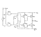
제6도는 상기 스테이틱 RAM에서 사용되는 본 발명의 센스증폭기 SA의 1실시예를 도시한 회로도이다.6 is a circuit diagram showing one embodiment of the sense amplifier SA of the present invention used in the static RAM.

이 센스증폭기 SA는 전단증폭기 A1과 후단증폭기 A2로 구성되는 것에 의해 고이득의 증폭기로 된다. 전단증폭기 A1은 제1동작전위점(GND)과 제2동작전위점(Vcc) 사이에 마련되고, 후단증폭기 A2는 마찬가지로 제3동작전위점(GND)의 제4동작전위점(Vcc) 사이에 마련된다. 이 실시예에서는 센스증폭기 SA는 차동모드에 결합된 한쌍의 MISFET Q201, Q202와 각 차등 MISFET의 드레인에 연결된 전류미러회로를 구성하는 한쌍의 능동부하 MISFET Q203, Q204로 형성된 제1의 비대칭형 차동증폭회로 P1, 제1의 비대칭형 차동증폭회로 P2과 같은 구성을 갖고 MISFET Q205~Q208로 구성된 제2의 비대칭형 차동증폭회로 P2, 비대칭형 차동증폭회로 P1 또는 P2와 같은 구성을 갖고 MISFET Q210~Q214로 구성된 제3의 비대칭형 차동증폭회로 P3으로 구성되어 있다.The sense amplifier SA is composed of a front end amplifier A1 and a rear end amplifier A2, resulting in a high gain amplifier. The shear amplifier A1 is provided between the first operating potential point GND and the second operating potential point Vcc, and the rear end amplifier A2 is likewise between the fourth operating potential point Vcc of the third operating potential point GND. Prepared. In this embodiment, the sense amplifier SA is a first asymmetric differential amplifier formed of a pair of MISFETs Q201 and Q202 coupled to the differential mode and a pair of active loads MISFETs Q203 and Q204 that constitute a current mirror circuit connected to the drain of each differential MISFET. The same configuration as the circuit P1, the first asymmetric differential amplifier circuit P2, and the second asymmetric differential amplifier circuit P2 composed of MISFETs Q205 to Q208, the asymmetric differential amplifier circuit P1 or P2, and the same configuration as the MISFET Q210 to Q214 And a third asymmetric differential amplifier circuit P3.

즉, 각각의 제1 및 제2의 비대칭형 차동증폭회로는 비반전 입력단자(+)에 결합된 게이트를 갖는 MISFET Q201 및 Q205, 반전입력단자(-)에 결합된 게이트와 MISFET Q201 및 Q205에 각각 결합된 소오스를 갖는 MISFET Q202 및 Q206, MISFET Q201, Q202, Q205, Q206의 각각의 드레인에 결합된 능동부하수단을 포함하는 비대칭형 차동증폭회로이며, 그 비반전 입력단자에서 받은 신호와 동상의 신호는 MISFET Q202 ,Q206의 드레인으로부터 얻어진다. 한편, 제3의 비대칭형 차동증폭회로 P3은 비반전 입력단자(+)에 결합된 게이트를 갖는 MISFET Q210, 반전입력단자(-)에 결합된 게이트와 MISFET Q210의 소오스에 결합된 소오스를 갖는 MISFET Q211, MISFET Q210및 Q211의 각각의 드레인에 결합된 능동부하수단을 포함하는 비대칭형 차동증폭회로이며, 그 비반전 입력단자(+)에서 받은 신호와 동상의 신호 D10는 MISFET Q211의 드레인으로부터 얻어진다.In other words, each of the first and second asymmetric differential amplifier circuits includes a gate coupled to a non-inverting input terminal (+), a gate coupled to an inverting input terminal (-), and a gate coupled to the MISFET Q201 and Q205. Asymmetric differential amplifier with active load means coupled to the respective drains of MISFETs Q202 and Q206, MISFETs Q201, Q202, Q205, and Q206, each having a coupled source, the asymmetric differential amplifier circuit of the signal and in-phase The signal is obtained from the drains of MISFETs Q202 and Q206. On the other hand, the third asymmetric differential amplifier circuit P3 has a MISFET Q210 having a gate coupled to the non-inverting input terminal (+), a MISFET having a gate coupled to the inverting input terminal (-) and a source coupled to the source of the MISFET Q210. Asymmetric differential amplifier circuit including active load means coupled to the respective drains of Q211, MISFET Q210 and Q211, and the signal D10 in phase and the signal received at its non-inverting input terminal (+) are obtained from the drain of MISFET Q211. .

제1 및 제2의 비대칭형 차동증폭회로 P1, P2는 각각 공통데이타

Figure kpo00051
Figure kpo00052
Figure kpo00053
Figure kpo00054
Figure kpo00055
Figure kpo00056
Figure kpo00057
Figure kpo00058
Figure kpo00059
Figure kpo00060
를 형성할 수 있고, 제2의 비대칭형 차동증폭회로 P2는 그의 전위가 신호 D1의 전위변화보다 크게 변화하는 출력신호 D1'를 형성할 수 있다. 전위 변화보다 크게 변화하는 출력신호 형성하고, 제2의 비대칭형 차동증폭회로 P2는 신호 D1의 전위변화와 같은 방향(동상)으로 그의 전위가 변하는 출력신호 D1'를 형성한다. 더우기, 제1 및 제2의 비대칭형 차동증폭회로 P1, P2의 부하 소자는 능동부하이다. 따라서, 제1의 비대칭형 차동증폭회로 P1은 그의 전위가 신호 전위변화와 같은 방향(동상)으로 그의 전위가 변하는 출력신호 D1가 인가된다. 결과적으로, 제1의 비대칭형 차동증폭회로 P1은 신호 공급된다. 비반전 입력단자(+)인 MISFET Q201, Q205의 게이트에는 각각 교차결선에 의한 신호 형성하고, 제2의 비대칭형 차동증폭회로 P2는 신호 D1의 전위가 변하는 방향과 같은 방향(동상)으로 그의 전위가 변하는 출력신호 D1'를 형성한다. 즉, 제1 및 제2의 비대칭형 차동증폭회로 P1, P2의 반전입력단자(-)인 MISFET Q202, Q206의 게이트에는 각각 신호 D1와 전위가 변하는 방향과 같은 방향(동상)으로 그의 전위가 변하는 출력신호 받는다. 제1의 비대칭형 차동증폭회로 P1은 신호 부터 신호 D1와 선쌍 CDL,The first and second asymmetric differential amplifier circuits P1 and P2 are common data, respectively.
Figure kpo00051
in
Figure kpo00052
To
Figure kpo00053
of
Figure kpo00054
To
Figure kpo00055
end
Figure kpo00056
Wow
Figure kpo00057
of
Figure kpo00058
To
Figure kpo00059
of
Figure kpo00060
And the second asymmetric differential amplifier circuit P2 can form an output signal D1 'whose potential varies more than the potential change of the signal D1. The output signal is changed to be larger than the potential change, and the second asymmetric differential amplifier circuit P2 forms the output signal D1 'whose potential is changed in the same direction (same phase) as the potential change of the signal D1. Moreover, the load elements of the first and second asymmetric differential amplifier circuits P1 and P2 are active loads. Therefore, the first asymmetric differential amplifier circuit P1 is applied with an output signal D1 whose potential changes in the same direction (same as the signal potential change). As a result, the first asymmetric differential amplifier circuit P1 is supplied with a signal. The gates of the MISFETs Q201 and Q205, which are non-inverting input terminals (+), form a signal by cross connection, respectively, and the second asymmetric differential amplifier circuit P2 has its potential in the same direction as the direction in which the potential of the signal D1 changes (in phase). Forms an output signal D1 'that is changed. That is, the gates of the MISFETs Q202 and Q206, which are the inverting input terminals (-) of the first and second asymmetric differential amplifier circuits P1 and P2, have their potentials changed in the same direction (same phase) as the direction in which the potentials of the signal D1 change. Receive the output signal. The first asymmetric differential amplifier P1 is a signal from the signal D1 and the line pair CDL,

본 실시예에서는 센스증폭기의 전압이득을 높이기 위해 전단증폭기 A1을 구성하는 제1 및 제2의 비대칭형 차동증폭회로 P1, P2에서의 출력신호 D1'와 D1'가 후단증폭기 A2를 구성하는 제3의 비대칭형 차동증폭회로 P3으로 인가된다.In the present embodiment, in order to increase the voltage gain of the sense amplifier, the output signals D1 'and D1' of the first and second asymmetrical differential amplifier circuits P1 and P2 constituting the shear amplifier A1 constitute a third amplifier A2. Is applied to asymmetric differential amplifier P3.

제3의 비대칭형 차동증폭회로 P3에서의 출력신호 out(D1")는 제5도에 도시한 데이타 출력버퍼 DOB의 입력단자 In으로 전달된다.The output signal out (D1 ") in the third asymmetric differential amplifier circuit P3 is transmitted to the input terminal In of the data output buffer DOB shown in FIG.

본 실시예에서는 제1 및 제2의 비대칭형 차동증폭회로 P1과 P2에 대해서 공통으로 정전류원을 구성하는 MISFET Q209가 배치되어 있다. MISFET Q209 대신에 각각의 비대칭형 차동증폭회로 P1, P2에 정전류원을 구성하는 MISFET를 배치하여도 된다.In this embodiment, the MISFET Q209 constituting a constant current source is disposed in common with the first and second asymmetric differential amplifier circuits P1 and P2. Instead of the MISFET Q209, a MISFET constituting a constant current source may be disposed in each of the asymmetric differential amplifier circuits P1 and P2.

제1, 제2와 제3의 차동증폭회로 P1, P2, P3은 각각 서로 상보적인 1쌍의 신호를 받아서 회로의 접지전위에 대해서 상보적인 신호 사이의 전위차에 대응하는 전위를 갖는 단일신호를 출력한다. 즉, 차동증폭회로는 2개의 신호를 받아서 하나의 신호만을 출력한다. 다른 차동증폭회로로서는 2개의 신호를 받아서 2개의 신호를 송출하는 형이 있다. 이러한 차동증폭회로를 상술한 차동증폭회로(예를들면P1, P2 또는 P3)와 구별하기 위해서 이하에서는 상술한 바와 같이 비대칭형 차동증폭회로라 한다.The first, second and third differential amplifier circuits P1, P2 and P3 each receive a pair of signals complementary to each other and output a single signal having a potential corresponding to the potential difference between the signals complementary to the ground potential of the circuit. do. That is, the differential amplifier circuit receives two signals and outputs only one signal. Another differential amplifier circuit is a type that receives two signals and sends two signals. In order to distinguish the differential amplifier circuit from the above-described differential amplifier circuit (for example, P1, P2 or P3), the differential amplifier circuit is referred to as an asymmetric differential amplifier circuit as described above.

바라는 센스증폭기가 제2도 a에 도시한 실시예에서와 같이 다수의 센스증폭기중에서 선택되는 경우, 정전류원으로서의 MSFET Q209, Q214는 제어신호 SAC를 받는 인버터회로 IV1, 메모리 어레이의 선택신호 m1를 받는 인버터회로IV2, MISFET Q215~Q218로 구성된 제어회로 CONT의 출력신호 SC에 의해 스위치 제어된다. 스위치수단(SW1, SW2)으로써의 상기 MISFET Q209 및 Q214가 동일한 제어신호 SC에 의해서 스위치 제어되는 것에 의해 전단증폭기 A1의 동작 기간과 후단증폭기 A2의 동작 기간을 용이하게 일치시킬 수가 있다. 따라서, 센스증폭기 SA가 2단 구성임에도 불구하고 그 동작, 비동작 타이밍을 정확하게 제어할 수가 있다.When the desired sense amplifier is selected from among a plurality of sense amplifiers as in the embodiment shown in FIG. 2A, MSFETs Q209 and Q214 as constant current sources receive inverter circuit IV1 receiving control signal SAC, selection signal m1 of memory array. The switch is controlled by the output signal SC of the control circuit CONT composed of inverter circuit IV2 and MISFET Q215 to Q218. Since the MISFETs Q209 and Q214 as the switch means SW1 and SW2 are controlled by the same control signal SC, it is possible to easily match the operation period of the front amplifier A1 and the operation period of the rear amplifier A2. Therefore, even if the sense amplifier SA has a two-stage configuration, the operation and non-operation timing can be precisely controlled.

이것에 대해서 제3도 a에 도시한 실시예에서와 같이 다수의 센스증폭기가 동시에 동작하는 경우, 제3도 b에 도시한 바와 같은 CS12가 정전류원으로써 MISFET Q209, Q214의 게이트에 인가된다.On the other hand, when a plurality of sense amplifiers operate simultaneously as in the embodiment shown in FIG. 3A, CS12 as shown in FIG. 3B is applied to the gates of the MISFETs Q209 and Q214 as constant current sources.

본 실시예에 따르면, 전단증폭기 A1에서는 2개의 비대칭형 차동증폭회로 P1, P2에 의해 평형신호 D1'와

Figure kpo00061
Figure kpo00062
Figure kpo00063
Figure kpo00064
의 전위는 신호 D1'의 전위의 상승값과 실질적으로 동일한 양으로 감소한다. 따라서, 이득을 더욱, 높이기 위해서 이와 동일한 비대칭형 차동증폭회로 P3을 후단증폭기 A2에 배치할 수 있다. 제1 및 제2의 비대칭형 차동증폭회로 P1, P2에 의해 형성된다. 특히, 신호 D1'의 전위가 상기 예와 같은 방법으로 상승했을때, 신호 대응해서 증폭된 신호 D1'와 형성된다. 즉, 상보적인 신호 D1와According to this embodiment, in the shear amplifier A1, the balanced signals D1 'and 2 are provided by two asymmetric differential amplifier circuits P1 and P2.
Figure kpo00061
end
Figure kpo00062
on
Figure kpo00063
Is
Figure kpo00064
The potential of decreases by an amount substantially equal to the rising value of the potential of the signal D1 '. Therefore, in order to further increase the gain, this same asymmetrical differential amplifier circuit P3 can be arranged in the post amplifier A2. The first and second asymmetric differential amplifier circuits P1 and P2 are formed. In particular, when the potential of the signal D1 'rises in the same manner as the above example, it is formed with the signal D1' amplified corresponding to the signal. That is, with the complementary signal D1

제1 및 제2의 비대칭형 차동증폭회로 P1, P2는 동일한 모놀리식 IC에 형성되는 것에 의해 서로 동일한 오프셋 전압을 가질 수 있다. 특히, 제1 및 제2의 비대칭형 차동증폭회로 P1, P2가 동일한 반도체 기판에 형성되어 있는 경우, 제조 조건등의 변화에 기인하는 제1의 비대칭형 차동증폭회로 P1을 구성하는 소자의 특성변화는 제2의 비대칭형 차동증폭회로 P2를 구성하는 소자의 특성 변화와 동일하게 된다. 그 결과, 구성 소자의 특성의 변화에 기인하는 제1의 비대칭형 차동증폭회로 P1의 오프셋도 소자의 특성의 변화에 기인하는 제2의 비대칭형 차동증폭회로 P2의 오프셋과 실질적으로 동일하게 된다. 제1의 비대칭형 차동증폭회로 P1의 입력단자(+), (-)에 그들 사이의 전위차를 0(V)로 하는 한쌍의 입력신호가 공급되었을때, 오프셋을 위하여 제1의 비대칭형 차동증폭회로 P1로부터 일정한 양(+)의 오프셋 전압이 가해진다고 가정한다. 그후, 제2의 비대칭형 차동증폭회로 P2에 제1의 비대칭형 차동증폭회로 P1과 같은 입력신호가 공급될때, 그의 오프셋을 위하여 제1의 비대칭형 차동증폭회로 P1에 공급된 오프셋 전압과 동일한 오프센전압을 공급한다.The first and second asymmetric differential amplifier circuits P1 and P2 may have the same offset voltage with each other by being formed in the same monolithic IC. In particular, when the first and second asymmetric differential amplifier circuits P1 and P2 are formed on the same semiconductor substrate, the characteristic change of the elements constituting the first asymmetric differential amplifier circuit P1 due to changes in manufacturing conditions, etc. Is equal to the characteristic change of the elements constituting the second asymmetric differential amplifier circuit P2. As a result, the offset of the first asymmetric differential amplifier P1 due to the change in the characteristics of the component also becomes substantially the same as the offset of the second asymmetric differential amplifier P2 due to the change in the characteristics of the device. When a pair of input signals having a potential difference of 0 (V) is supplied to the input terminals (+) and (-) of the first asymmetric differential amplifier circuit P1, the first asymmetric differential amplifier is offset for offset. It is assumed that a certain positive offset voltage is applied from the circuit P1. Then, when an input signal such as the first asymmetric differential amplifier P1 is supplied to the second asymmetric differential amplifier P2, the offset voltage equal to the offset voltage supplied to the first asymmetric differential amplifier P1 is offset for its offset. Supply high voltage.

따라서, 비대칭형 차동증폭회로 P1, P2에 의해 형성된 출력신호 D1'와

Figure kpo00065
Figure kpo00066
는 각각 제3의 비대칭형 차동증폭회로 P3에 인가된다. 이 제3의 비대칭형 차동증폭회로 P3은 차동증폭회로이므로, P1, P2에서 공급되는 2입력신호의 차전압이 P3에 의해서 증폭된다. 즉, 2입력신호가 동상 신호인 경우에는 P3에 의한 증폭동작은 실행되지 않는다. 따라서, 각 입력신호에 동상의 오프셋 전압이 발생하여도 P3은 이것을 상쇄할 수가 있다. 즉 출력신호 D1'에 포함된 제1의 비대칭형 차동증폭회로 P1의 오프셋 전압과 출력신호 D1'에 포함된 제2의 비대칭형 차동증폭회로 P2의 오프셋 전압을 상쇄시킬 수 있다. 따라서, 제1 및 제2의 비대칭형 차동증폭회로 P1, P2의 오프셋 전압은 출력 신호 out(D1")에 포함되지 않는다. 제3의 비대칭형 차동증폭회로 P3의 출력신호 P3out(D1")의 신호레벨은 충분히 크므로, 상기의 오프셋 전압은 실질적으로 무시할 수가 있다. 서로 동일한 오프셋 전압을 포함한다. 출력신호 D1'와Therefore, the output signals D1 'formed by the asymmetric differential amplifier circuits P1 and P2
Figure kpo00065
Is
Figure kpo00066
Are respectively applied to the third asymmetric differential amplifier P3. Since the third asymmetric differential amplifier circuit P3 is a differential amplifier circuit, the difference voltage of the two input signals supplied from P1 and P2 is amplified by P3. That is, when the two input signals are in phase signals, the amplification operation by P3 is not performed. Therefore, even if an offset voltage of in phase occurs in each input signal, P3 can cancel this out. That is, the offset voltage of the first asymmetric differential amplifier circuit P1 included in the output signal D1 'and the offset voltage of the second asymmetric differential amplifier circuit P2 included in the output signal D1' may be canceled. Therefore, the offset voltages of the first and second asymmetric differential amplifier circuits P1 and P2 are not included in the output signal out (D1 "). The output signal P3out (D1") of the third asymmetric differential amplifier circuit P3 is not included. Since the signal level is sufficiently large, the above offset voltage can be substantially ignored. Include offset voltages that are equal to each other. With output signal D1 '

비대칭형 차동증폭회로 P2, P1의 오프셋은 제3의 비대칭형 차동증폭회로 P3에서 상쇄되므로, 정전류원을 구성하는 MISFET Q209, Q214는 동시에 동작할 수 있다. 따라서, 출력신호 out(D1")는 고속으로 출력된다. 따라서, 스테이틱 RAM의 동작이 고속으로 된다.Since the offsets of the asymmetric differential amplifiers P2 and P1 are offset by the third asymmetric differential amplifier circuit P3, the MISFETs Q209 and Q214 constituting the constant current source can operate simultaneously. Therefore, the output signal out (D1 ") is output at high speed. Therefore, the operation of the static RAM becomes high speed.

동상의 잡음이 입력신호 D1와

Figure kpo00067
Figure kpo00068
에 남는 경우에도 회로 P3이 차동증폭회로이므로, 그것을 상쇄하여 다음 단으로 전달되지 않는다. 작용하는 경우에도 회로 P1과 P2가 차동증폭회로이므로 그것을 상쇄할 수 있다. 따라서, 잡음은 다음 단으로 전달되지 않는다. 마찬가지로, 동상의 잡음이 출력신호 D1'와In-phase noise with input signal D1
Figure kpo00067
on
Figure kpo00068
The circuit P3 is a differential amplification circuit even if it remains at, so it is canceled and not transferred to the next stage. Even in the case of operation, since circuits P1 and P2 are differential amplifiers, they can be canceled out. Therefore, noise is not transmitted to the next stage. Similarly, the in-phase noise is equal to the output signal D1 '.

상술한 바와 같이 본 발명의 실시예에 따르면, 차

Figure kpo00069
Figure kpo00070
Figure kpo00071
사이의 전압차가 0.2(V)보다 작은 경우에도 이 실시예의 센스증폭기 SA는 데이타 출력버퍼 DOB를 충분히 구동시킬 수 있는 큰 출력신호를 형성할 수 있으므로, 스테이틱 RAM을 고속화할 수 있다.서의 신호 D1, 이의 전위차가 비교적 작은 경우에도 센스증폭기는 데이타 출력버퍼를 만족스럽게 구동시킬 수 있다. 따라서, 센스증폭기는 서로 상보적인 정보쌍이 메모리셀에서 데이타선쌍 D, D에 출력된 후의 단시간내에 데이타 출력버퍼를 구동시킬 수 있다. 그러므로, 스테이틱 RAM의 고속동작화를 달성할 수가 있다. 예를들면, 공통데이타선쌍 CDL과 동증폭회로에 포함된 오프셋 전압과 잡음의 영향을 줄이고, 고감도와 고이득을 갖는 센스증폭기를 제공할 수 있다. 이때문에, 공통데이타선쌍에서의 신호 D1와As described above, according to the embodiment of the present invention,
Figure kpo00069
four
Figure kpo00070
on
Figure kpo00071
Even when the voltage difference between them is smaller than 0.2 (V), the sense amplifier SA of this embodiment can form a large output signal capable of sufficiently driving the data output buffer DOB, thereby speeding up the static RAM. Even when D1 and its potential difference are relatively small, the sense amplifier can satisfactorily drive the data output buffer. Therefore, the sense amplifier can drive the data output buffer within a short time after the information pairs complementary to each other are outputted to the data line pairs D and D from the memory cell. Therefore, high speed operation of the static RAM can be achieved. For example, it is possible to reduce the influence of offset voltage and noise included in the common data line pair CDL and the copper amplifier circuit, and to provide a sense amplifier having high sensitivity and high gain. For this reason, the signal D1 in the common data line pair

제6도에 도시한 비대칭형 차동증폭회로는 게이트와 드레인이 서로 교차결선된 한쌍의 MISFET를 포함하는 래치회로로 대체시킬 수 있다. 그러나, 이러한 경우에는 래치회로에 유지된 상태를 해제하거나 래치회로를 반대의 상태로 하기 위해 비교적 긴 시간이 요구된다. 따라서, 스테이틱 RAM의 동작 속도가 제한되어 스테이틱 RAM을 고속화할 수 없다.The asymmetric differential amplifier circuit shown in FIG. 6 can be replaced with a latch circuit including a pair of MISFETs whose gate and drain are cross-connected with each other. In this case, however, a relatively long time is required to release the state held in the latch circuit or to reverse the latch circuit. Therefore, the operation speed of the static RAM is limited and the static RAM cannot be speeded up.

특히, 앞서 설명한 것과 같이 센스증폭기의 출력신호가 하이레벨 또는 로우레벨

Figure kpo00072
사이의 비교는 2개의 신호의 상대적 전위 사이의 비교이며, 센스증폭기의 출력신호와 상술한 바와 같은 제조 조건에 따라 값이 변하는 기준전압(임계전압) 사이의 비교와는 달리 제조 조건의 변화에 덜 민감하다. 따라서, 오동작이 적은 스테이틱 RAM을 제공할 수가 있다.인지의 여부가 센스증폭기로부터의 출력신호의 전위가 회로의 접지전위에 대해서 데이타 출력버퍼의 논리 임계전압보다 높거나 낮은가의 여부에 따라서 검출되는 경우에, 데이타 출력버퍼의 잡음 마진은 제조 조건의 변화에 기인하는 논리 임계전압의 변화에 의해 작아진다. 한편, 평형신호 D1'와In particular, as described above, the output signal of the sense amplifier is high level or low level.
Figure kpo00072
The comparison between is a comparison between the relative potentials of the two signals, and unlike the comparison between the output signal of the sense amplifier and the reference voltage (threshold voltage) whose value varies depending on the manufacturing conditions as described above, it is less likely to change the manufacturing conditions. be sensitive. Therefore, it is possible to provide a static RAM with less malfunctions. Whether the potential of the output signal from the sense amplifier is higher or lower than the logic threshold voltage of the data output buffer with respect to the ground potential of the circuit is detected. In the case, the noise margin of the data output buffer is small due to the change in the logic threshold voltage due to the change in manufacturing conditions. On the other hand, the equilibrium signal D1 'and

제7도는 본 발명의 또 다른 실시예의 블럭도이다.7 is a block diagram of another embodiment of the present invention.

본 실시예에서, 전단증폭기 A1은 상술한 것과 마찬가지인 비대칭형 차동증폭회로 P1과

Figure kpo00073
Figure kpo00074
를 형성한다. 각각의 비대칭형 차동증폭회로 P1, P2, P4, P5의 구체적인 회로는 제6도와 동일하므로 다시 반복하여 설명하지 않는다. 형성한다. 그리고, 후단증폭기 A2는 상술한 것과 마찬가지인 비대칭형 차동증폭회로 P4와 P5를 배치하는 것에 의해 구성되어 평형출력신호 OUT, P2에 의해 구성되고, 평형신호 D1'와In this embodiment, the shear amplifier A1 is equal to the asymmetric differential amplifier circuit P1 as described above.
Figure kpo00073
To
Figure kpo00074
To form. Specific circuits of the asymmetric differential amplifier circuits P1, P2, P4, and P5 are the same as those of FIG. 6 and will not be described again. Form. The rear stage amplifier A2 is constituted by arranging the asymmetric differential amplifier circuits P4 and P5 similar to those described above, and is composed of the balanced output signals OUT and P2, and the balanced signals D1 'and

평형출력신호 OUT와

Figure kpo00075
Figure kpo00076
Figure kpo00077
가 센스증폭기의 출력신호로 된다. 따라서, 이 센스증폭기의 출력신호 사이의 전위차는 제6도에 도시한 센스증폭기의 출력신호 out의 진폭의 약 2배로 된다. 즉, 본 실시예의 센스증폭기는 제6도에 도시한 센스증폭기 SA보다 약 2배의 이득을 갖는다. 각 게이트회로 G101과 G102의 한쪽의 입력단자 T1과 T2에 직접 입력된다. 따라서, 데이타 출력버퍼 DOB를 간략화할 수 있다. 이 실시예에서는 평형신호 OUT와 제5도의 데이타 출력버퍼 DOB에 공급하는 경우에는 데이타 출력버퍼 DOB내의 인버터회로 G103이 생략되며, 출력신호 OUT와With balanced output signal OUT
Figure kpo00075
To
Figure kpo00076
Is
Figure kpo00077
Becomes the output signal of the sense amplifier. Therefore, the potential difference between the output signals of this sense amplifier is about twice the amplitude of the output signal out of the sense amplifier shown in FIG. In other words, the sense amplifier of this embodiment has a gain approximately twice that of the sense amplifier SA shown in FIG. It is directly input to one input terminal T1 and T2 of each gate circuit G101 and G102. Therefore, the data output buffer DOB can be simplified. In this embodiment, the inverter circuit G103 in the data output buffer DOB is omitted when the balanced signal OUT and the data output buffer DOB of FIG. 5 are supplied.

또한, 본 실시예에서 비대칭형 차동증폭회로 P1,

Figure kpo00078
Figure kpo00079
Figure kpo00080
사이의 전위차는 오프셋 전압보다 충분히 크므로, 이 오프셋 전압은 실질적으로 무시된다. 각각 포함된다. 그러나, 출력신호 OUT와 포함되지 않는다. 비대칭형 차동증폭회로 P4와 P5의 오프셋 전압은 출력신호 OUT와 P2를 동일한 반도체 기판에 형성하는 것에 의해 비대칭형 차동증폭회로 P1, P2에 포함된 오프셋 전압은 제6도에서 설명한 것과 같은 이유로 해서 비대칭형 차동증폭회로 P4와 P5에서 상쇄된다. 따라서, 비대칭형 차동증폭회로 P1과 P2의 오프셋 전압은 출력신호 OUT와In addition, in the present embodiment, the asymmetric differential amplifier P1,
Figure kpo00078
on
Figure kpo00079
on
Figure kpo00080
Since the potential difference between them is sufficiently larger than the offset voltage, this offset voltage is substantially ignored. Each is included. However, it is not included with the output signal OUT. The offset voltages of the asymmetric differential amplifier circuits P4 and P5 form the output signals OUT and P2 on the same semiconductor substrate, so that the offset voltages included in the asymmetric differential amplifier circuits P1 and P2 are asymmetric for the same reason as described in FIG. Type differential amplifiers are canceled in P4 and P5. Therefore, the offset voltages of the asymmetric differential amplifier circuits P1 and P2 are not equal to the output signal OUT.

동상 잡음이 신호 D1와

Figure kpo00081
Figure kpo00082
Figure kpo00083
Figure kpo00084
Figure kpo00085
의 각각의 전위는 잡음에 의해 변하지 않는다. 모두 작용할 때에도 출력신호 OUT와 및 신호 D1'. 남은 경우에도 비대칭형 차동증폭회로 P4와 P5에서 이것을 상쇄시킬 수 있다. 따라서, 동상 잡음이 신호 D1, 남을 경우에 비대칭형 차동증폭회로 P1과 P2에서 이 잡음을 상쇄시킬 수 있다. 마찬가지로, 동상 잡음이 신호 D1'와In-phase noise signal D1
Figure kpo00081
on
Figure kpo00082
on
Figure kpo00083
Figure kpo00084
on
Figure kpo00085
Each potential of is not changed by noise. Output signal OUT and and signal D1 'are both active. The remaining cases can be offset by asymmetric differential amplifiers P4 and P5. Therefore, if the in-phase noise remains in the signal D1, the asymmetric differential amplifiers P1 and P2 can cancel this noise. Similarly, frostbite noise with signal D1 '

상술한 바와 같이, 이 실시예에 따르면 오프셋 전압과 잡음의 영향을 한층 더 감소시키고, 고감도와 고이득을 갖는 센스증폭기를 제공할 수가 있다.As described above, according to this embodiment, it is possible to further reduce the influence of offset voltage and noise, and to provide a sense amplifier having high sensitivity and high gain.

제8도는 비대칭형 차동증폭회로 P의 또 다른 실시예의 회로도이다.8 is a circuit diagram of another embodiment of the asymmetric differential amplifier circuit P. FIG.

이 실시예에서 비대칭형 차동증폭회로는 차동모드에 연결된 1쌍의 MISFET Q219 및 Q220, 게이트가 접지되고 MISFET Q219의 부하로써 기능하는 MISFET Q225, MISFET Q219 와 Q221의 공통드레인이 게이트에 접속된 MISFET Q222로 구성되어 있다. 이 실시예의 비대칭형 차동증폭회로 P는 전류미러회로를 부하로서 사용하는 비대칭형 차동증폭회로, 예를들면 제6도에 도시한 비대칭형 차동증폭회로 P1과 비교하여 보다 높은 이득을 갖는다. 그러나, 이 회로는 비교적 높은 오프셋 전압을 갖게 된다. 특히, 비대칭형 차동증폭회로 P에 있어서, MISFET Q221은 비교적 큰 저항을 갖는 부하로서동작한다. 따라서, MISFET Q222의 게이트와 소오스 사이에 비교적 큰 전압을 인가하는 것이 허용된다. 그 결과, 비대칭형 차동증폭회로 P는 높은 이득을 갖는다. 그러나, MISFET Q219와 MISFET Q220의 특성은, 예를들어 제조 조건의 변화에 의해 일치하지 않는다. 이러한 경우, 비반전 입력단자(+)와 반전입력단자(-)에 동일한 전위의 입력신호를 인가하여도 MISFET Q219의 드레인 전류는 MISFET Q220의 드레인 전류보다 커지며, MISFET Q221이 비교적 큰 저항을 갖는 부하이므로 MISFET Q222의 게이트와 소오스 사이에 비교적 큰 전압이 인가된다. 따라서, MISFET Q222의 상호 콘덕턴스가 높아져서 큰 값의 전류가 제공된다. 즉, 비대칭형 차동증폭회로 P는 비교적 큰 오프셋 전압을 갖는다.In this embodiment, the asymmetric differential amplifier circuit comprises a pair of MISFETs Q219 and Q220 connected in differential mode, a MISFET Q222 gated to ground and a common drain of MISFET Q219 and Q221 connected to the gate of the MISFET Q219. Consists of The asymmetrical differential amplifier P of this embodiment has a higher gain compared to the asymmetrical differential amplifier circuit using the current mirror circuit as a load, for example, the asymmetrical differential amplifier circuit P1 shown in FIG. However, this circuit has a relatively high offset voltage. In particular, in the asymmetric differential amplifier circuit P, the MISFET Q221 operates as a load having a relatively large resistance. Thus, it is allowed to apply a relatively large voltage between the gate and the source of the MISFET Q222. As a result, the asymmetrical differential amplifier P has a high gain. However, the characteristics of the MISFET Q219 and the MISFET Q220 do not coincide due to changes in manufacturing conditions, for example. In this case, even when an input signal having the same potential is applied to the non-inverting input terminal (+) and the inverting input terminal (-), the drain current of the MISFET Q219 becomes larger than the drain current of the MISFET Q220, and the load of which the MISFET Q221 has a relatively large resistance is increased. Therefore, a relatively large voltage is applied between the gate and the source of MISFET Q222. Thus, the mutual conductance of the MISFET Q222 is increased to provide a large value of current. In other words, the asymmetric differential amplifier P has a relatively large offset voltage.

그러나, 제8도에 도시한 바와 같이 비대칭형 차동증폭회로가 제6도 또는 제7도의 비대칭형 차동증폭회로 P1과 P2에 사용되는 경우에는 오프셋 전압을 상쇄할 수 있다. 따라서, 오프셋 전압은 아무런 문제를 일으키지 않아 높은 이득을 활용할 수 있다.However, as shown in FIG. 8, when the asymmetric differential amplifier circuits are used in the asymmetric differential amplifier circuits P1 and P2 of FIG. 6 or 7, the offset voltage can be canceled. Therefore, the offset voltage does not cause any problem and can utilize a high gain.

제9도는 제6도 또는 제7도의 비대칭형 차동증폭회로 P1과 P2가 모놀리식 IC에 형성된 경우의 배치도이다.FIG. 9 is a layout view when the asymmetric differential amplifier circuits P1 and P2 of FIG. 6 or 7 are formed in a monolithic IC.

제9도에 있어서, 굵은 실선으로 둘러싸인 부분은 알루미늄 배선층을 나타낸다. 알루미늄 배선층은 공급전압 Vcc의 배선층, 회로의 접지전위 GND의 배선층, 차동 MISFET Q201, Q202와 Q205, Q206의 공통소오스층의 접속용 배선층 및 차동 MISFET의 드레인층과 부하 MISFET 의 드레인층을 접촉하기 위한 배선층으로 사용된다.In FIG. 9, the part enclosed by a thick solid line shows an aluminum wiring layer. The aluminum wiring layer is used for contacting the wiring layer of the supply voltage Vcc, the wiring layer of the ground potential GND of the circuit, the connection wiring layer of the common source layer of the differential MISFETs Q201, Q202, Q205 and Q206, and the drain layer of the differential MISFET and the drain layer of the load MISFET. Used as a wiring layer.

제9도에서, 가는 실선으로 둘러싸인 부분은 도전성 다결정 실리콘층을 나타낸다. 도전성 다결정 실리콘층은 각각의 MISFET의 게이트전극과 그것과 관련된 배선층으로 사용된다.In FIG. 9, the portion surrounded by the thin solid line represents the conductive polycrystalline silicon layer. The conductive polycrystalline silicon layer is used as the gate electrode of each MISFET and its associated wiring layer.

점선으로 둘러싸인 부분은 P형 또는 N형 확산층을 나타낸다. 이 확산층은 MISFET의 소오스층 또는 드레인층 및 차동 MISFET의 게이트를 접속하기 위한 배선층으로 사용된다.The part enclosed by the dotted line represents a P type or N type diffusion layer. This diffusion layer is used as a source layer or drain layer of the MISFET and a wiring layer for connecting the gate of the differential MISFET.

그리고, 일점쇄선으로 둘러싸인 부분은 n형 기판에 형성된 P형 웰층을

Figure kpo00086
표는 콘택트를 나타낸다.나타낸다. 따라서, P형 웰내에 N채널 MISFET가 형성된다. 또The portion surrounded by the dashed line is a P-type well layer formed on the n-type substrate.
Figure kpo00086
The table shows the contacts. Thus, an N-channel MISFET is formed in the P-type well. In addition

본 발명은 상술한 실시에에 한정되는 것은 아니다.This invention is not limited to the above-mentioned embodiment.

스테이틱형 RAM의 시스템 구성은 여러가지의 실시형태를 채택할 수 있다.The system configuration of the static RAM can adopt various embodiments.

Claims (23)

한쌍의 상보적인 신호(D1,
Figure kpo00087
)
Figure kpo00088
)
Figure kpo00089
)
Figure kpo00090
))
Figure kpo00092
)
Figure kpo00093
)
Figure kpo00094
)
Figure kpo00095
)와의 차신호에 따라서 하나의 출력신호(out)를 형성하기 위한 수단을 구비한 제3의 비대칭형 차동증폭회로(P3)를 갖는 후단증폭기(A2), 상기 후단증폭기(A2)의 출력신호(out)에 따라서 출력데이타(Dout)를 얻기위한 데이타 출력버퍼(DOB)를 동일의 모놀리식 IC내에 형성하여 이루어지고, 상기 데이타 출력버퍼(DOB)는 또, 상기 출력데이타(Dout)를 얻기 위한 트랜지스터(Q105,Q106)과 이 트랜지스터(Q105,Q<SB.106)의 출력의 출력제어신호(WE, OE)에 따르는 신호(Cont)에 의해서 저출력 임피던스상태 또는 고출력 임피던스상태로 하기 위한 게이트회로(G,SB>101,G102)를 가지며, 상기 각각의 제1 및 제2의 비대칭형 차동증폭회로(P1, P2)는 상기 제1 및 제2의 비반전 입력단자(+)에 결합된 게이트를 갖는 제1의 도전형의 제1의 절연게이트형 전계효과 트랜지스터(Q<SB.201,Q205), 상기 제1 및 제2의 반전입력단자(-)에 결합된 게이트와 상기 제1의 절연게이트형 전계효과 트랜지스터의 소오스에 결합된 소오스를 갖는 상기 제1의 도전형의 제2의 절연게이트형 전계효과 트랜지스터(Q201,Q206), 상기 제1 및 제2의 절연게이트형 전계효과 트랜지스터의 각각의 드레인에 결합된 제2의 도전형의 절연게이트형 전계효과 트랜지스터를 포함하는 제1의 능동부하수단(Q203, Q204, Q207, Q208>/SB>, Q 221, Q222)를 포함하고, 상기 제1 및 제2의 비반전 입력단자(+)에서 받은 상기 신호와 동상의 신호(D1', D1')를 상기 제2의 절연게이트형 전계효과 트랜지스터의 상기 드레인에서 얻는 구성으로 하고, 상기 제3의 비대칭형 차동증폭회로(P3)은 상기 제3의 반전입력단자(-)에 결합된 게이트를 갖는 제1의 도전형의 제5의 절연게이트형 전계효과 트랜지스터(Q,SB>211), 상기 제3의 비반전 입력단자(+)에 결합된 게이트와 상기 제5의 절연게이트형 전계효과 트랜지스터(Q210), 상기 제5 및 제6의 절연게이트형 전계효과 트랜지스터의 각각의 드레인에 결합된 제2의 도전형의 절연게이트형 전계효과 트랜지스터를 포함하는 제2의 능동부하수단(Q212, Q213, Q221, Q<SB.222)을 포함하고, 상기 제3의 비반전 입력단자(+)에서 받은 상기 신호와 동상의 신호(out)를 상기 제5의 절연게이트형 전계효과 트랜지스터(Q211)의 상기 드레인에서 얻는 구성으로 한 증폭기를 갖는 반도체 기억장치.
A pair of complementary signals (D1,
Figure kpo00087
)
Figure kpo00088
)
Figure kpo00089
)
Figure kpo00090
) )
Figure kpo00092
)
Figure kpo00093
)
Figure kpo00094
)
Figure kpo00095
And a post amplifier A2 having a third asymmetric differential amplifier circuit P3 having means for forming one output signal out in accordance with the difference signal from A data output buffer (DOB) for obtaining output data (Dout) is formed in the same monolithic IC according to out, and the data output buffer (DOB) is also used for obtaining the output data (Dout). For the low output impedance state or the high output impedance state by the transistors Q 105 and Q 106 and the signals Cont according to the output control signals WE and OE of the outputs of the transistors Q 105 and Q <SB.106, Gate circuits (G, SB> 101, G102 ), each of said first and second asymmetric differential amplifier circuits (P1, P2) connected to said first and second non-inverting input terminals (+). isolation of the first conductivity type having a first gate coupled to the gate type field effect transistor (Q <SB.201, Q 205) , the The second insulated gate field effect transistor of the first conductivity type having a gate coupled to the first and second inverting input terminals (-) and a source coupled to the source of the first insulated gate field effect transistor. (Q 201 , Q 206 ), a first active load means comprising a second conductivity type insulated gate field effect transistor coupled to each drain of the first and second insulated gate type field effect transistors ( Q 203 , Q 20 4, Q 207 , Q 208> / SB>, Q 221 , Q 222 , and the signal in phase with the signal received from the first and second non-inverting input terminals (+) ( D1 'and D1' are obtained from the drain of the second insulated gate field effect transistor, and the third asymmetric differential amplifier circuit P3 is connected to the third inverting input terminal (-). A fifth insulated gate field effect transistor (Q, SB> 211) of the first conductivity type having a coupled gate, A gate coupled to the third non-inverting input terminal (+) and coupled to a drain of each of the fifth insulating gate type field effect transistor Q 210 and the fifth and sixth insulating gate type field effect transistors. A second active load means (Q 212 , Q 213 , Q 221 , Q <SB.222) comprising a second conductive type insulated gate field effect transistor, wherein the third non-inverting input terminal A semiconductor memory device having an amplifier configured to obtain the signal (out) in phase with the signal received at (+) from the drain of the fifth insulated gate field effect transistor (Q 211 ).
특허청구의 범위 제1항에 있어서, 상기 전단증폭기(A1)은 또, 상기 전단증폭기(A1)의 동작타이밍을 제어하기 위한 제1의 스위치수단(Q209)를 갖고, 상기 후단증폭기(A2)는 또, 상기 후단증폭기(A2)의 동작타이밍을 제어하기 위한 제2의 스위치수단(Q<SB.214)을 가지며, 상기 제1 및 제2의 스위치수단(Q209,Q214)는 동일한 제어신호(SC)에 의해서 동시에 제어되는 것을 특징으로 하는 증폭기를 갖는 반도체 기억장치.The claim 1, wherein the shear amplifier A1 further has a first switch means Q 209 for controlling the operation timing of the shear amplifier A1, and the rear amplifier A2. In addition, has a second switch means (Q <SB.214) for controlling the operation timing of the rear-end amplifier (A2), the first and second switch means (Q 209 , Q 214 ) is the same control A semiconductor memory device having an amplifier, which is controlled simultaneously by a signal SC. 특허청구의 범위 제2항에 있어서, 상기 제1의 능동부하수단은 그의 드레인이 상기 제2의 절연게이트형 전계효과 트랜지스터(Q202,Q206)의 드레인에 결합되고, 그의 게이트가 상기 제1의 도전형의 제1의 절연게이트형 전계효과 트랜지스터(Q201,Q205)의 드레인에 결합된 제2의 도전형의 제3의 절연게이트형 전계효과 트랜지스터(Q204,Q208)과 그의 소오스가 상기 제3의 절연게이트형 전계효과 트랜지스터의 소오스에 결합되고, 그의 게이트와 드레인이 상기 제3의 절연게이트형 전계효과 트랜지스터의 게이트에 결합된 제2의 도전형의 제4의 절연게이트형 전계효과 트랜지스터(Q203,Q207)를 갖는 제1의 전류미러회로를 포함하고, 상기 제2의 농동부하수단은 그의 드레인이 상기 제5의 절연게이트형 전계효과 트랜지스터(Q211)의 드레인에 결합되고, 그의 게이트가 상기 제6의 절연게이트형 전계효과 트랜지스터(Q<SB.210)의 드레인에 결합된 제2의 도전형의 제7의 절연게이트형 전계효과 트랜지스터(Q213)과 그의 소오스가 상기 제7의 절연게이트형 전계효과 트랜지스터의 소오스에 결합되고, 그의 게이트와 드레인이 상기 제7의 절연게이트형 전계효과 트랜지스터의 게이트에 결합된 상기 제2의 도전형의 제8의 절연게이트형 전계효과 트랜지스터(Q212)를 갖는 제2의 전류미러회로를 포함하는 것을 특징으로 하는 증폭기를 갖는 반도체 기억장치.The method of claim 2, wherein the first active load means has a drain coupled to a drain of the second insulated gate field effect transistors Q 202 and Q 206 , the gate of which is coupled to the first active load means. The third insulated gate type field effect transistors Q204 and Q208 of the second conductive type coupled to the drains of the first insulated gate type field effect transistors Q 201 and Q 205 of the conductive type and the source thereof are A fourth insulated gate field effect transistor of a second conductivity type coupled to the source of a third insulated gate field effect transistor, the gate and drain of which are coupled to the gate of the third insulated gate field effect transistor; A first current mirror circuit having (Q 203 , Q 207 ), the second concentrated load means having a drain coupled to the drain of the fifth insulated gate field effect transistor (Q 211 ); , His gay In that said sixth insulating gate type field effect transistor (Q <SB.210) a second conductivity type seventh insulating gate type field effect transistor (Q 213) and its source is the seventh in the coupled to the drain of the An eighth insulated gate field effect transistor (Q) of the second conductivity type, coupled to the source of the insulated gate field effect transistor, whose gate and drain coupled to the gate of the seventh insulated gate field effect transistor (Q) And a second current mirror circuit having a second current mirror circuit ( 212 ). 특허청구의 범위 제1항에 있어서, 상기 제1의 능동부하수단은 그의 드레인이 상기 제2의 절연게이트형 전계효과 트랜지스터(Q202,Q206)의 드레인에 결합되고, 그의 게이트가 상기 제1의 도전형의 제1의 절연게이트형 전계효과 트랜지스터(Q201,Q205)의 드레인에 결합된 제2의 도전형의 제3의 절연게이트형 전계효과 트랜지스터(Q204,Q208)과 그의 소오스가 상기 제3의 절연게이트형 전계효과 트랜지스터의 소오스에 결합되고, 그의 게이트와 드레인이 상기 제3의 절연게이트형 전계효과 트랜지스터의 게이트에 결합된 제2의 도전형의 제4의 절연게이트형 전계효과 트랜지스터(Q203,Q207)를 갖는 제1의 전류미러회로를 포함하고, 상기 제2의 농동부하수단은 그의 드레인이 상기 제5의 절연게이트형 전계효과 트랜지스터(Q2211)의 드레인에 결합되고, 그의 게이트가 상기 제6의 절연게이트형 전계효과 트랜지스터(Q210)의 드레인에 결합된 제2의 도전형의 제7의 절연게이트형 전계효과 트랜지스터(Q213)과 그의 소오스가 상기 제7의 절연게이트형 전계효과 트랜지스터의 소오스에 결합되고, 그의 게이트와 드레인이 상기 제7의 절연게이트형 전계효과 트랜지스터의 게이트에 결합된 상기 제2의 도전형의 제8의 절연게이트형 전계효과 트랜지스터(Q212)를 갖는 제2의 전류미러회로를 포함하는 것을 특징으로 하는 증폭기를 갖는 반도체 기억장치.The method of claim 1, wherein the first active load means has a drain thereof coupled to a drain of the second insulated gate field effect transistors Q 202 and Q 206 , the gate of which is the first one. The third insulated gate type field effect transistors Q 204 and Q 208 of the second conductive type coupled to the drains of the first insulated gate type field effect transistors Q 201 and Q 205 of the conductive type and its source Is coupled to the source of the third insulated gate field effect transistor, and the fourth insulated gate type electric field of the second conductivity type whose gate and drain are coupled to the gate of the third insulated gate field effect transistor. A first current mirror circuit having effect transistors Q 203 and Q 207 , wherein the second concentrated load means has a drain thereof at the drain of the fifth insulated gate field effect transistor Q 2 211 . Combined, his crab The seventh insulated gate field effect transistor Q 213 of the second conductivity type coupled to the drain of the sixth insulated gate type field effect transistor Q 210 and its source are the seventh insulated gate. type field effect is coupled to the source of the transistor, its gate and drain of said second insulating gate type field of conductive eighth of the effects coupled to the gate of the seventh insulating gate type field effect transistor of the transistor (Q 212) And a second current mirror circuit having an amplifier. 특허청구의 범위 제1항에 있어서, 상기 데이타 출력버퍼(DOB)는 출력데이타(Dout)를 얻기 위해 서로 직렬로 접속된 제1의 출력트랜지스터(Q105)와 제2의 출력트랜지스터(Q106), 상기 제1의 출력트랜지스터(Q105)의 출력을 출력제어신호(WE, OE)에 따르는 신호(Cont)에 의해서 저출력 임피던스상태 또는 고출력 임피던스상태로 하기 위한 제1의 게이트회로(G,SB>101), 상기 제2의 출력트랜지스터(Q106)의 출력을 출력제어신호(WE, OE)에 따르는 신호(Cont)에 의해서 저출력 임피던스상태 또는 고출력 임피던스상태로 하기 위한 제2의 게이트회로(G102)를 구비하고, 상기 제1의 게이트회로(G101) 및 상기 제2의 게이트회로(G102)는 상기 제1의 출력트랜지스터(Q105) 또는 제2의 출력트랜지스터(Q106)이 저출력 임피던스상태일때에 상기 후단증폭기(A2)에 따라서 동작하는 것을 특징으로 하는 증폭기를 갖는 반도체 기억장치.The data output buffer (DOB) of claim 1 is a first output transistor (Q 105 ) and a second output transistor (Q 106 ) connected in series with each other to obtain an output data (Dout). And a first gate circuit G, SB> 101 for bringing the output of the first output transistor Q105 into a low output impedance state or a high output impedance state by a signal Cont according to the output control signals WE and OE. ), A second gate circuit G 102 for setting the output of the second output transistor Q 106 to a low output impedance state or a high output impedance state by a signal Cont according to the output control signals WE and OE. The first gate circuit G 101 and the second gate circuit G 102 have a low output impedance state in which the first output transistor Q 105 or the second output transistor Q 106 is in a low output impedance state. To operate according to the rear end amplifier A2. A semiconductor memory device having an amplifier with a gong. 특허청구의 범위 제3항에 있어서, 상기 데이타 출력버퍼(DOB)는 출력데이타(Dout)를 얻기 위해 서로 직렬로 접속된 제1의 출력트랜지스터(Q105)와 제2의 출력트랜지스터(Q106), 상기 제1의 출력트랜지스터(Q105)의 출력을 출력제어신호(WE, OE)에 따르는 신호(Cont)에 의해서 저출력 임피던스상태 또는 고출력 임피던스상태로 하기 위한 제1의 게이트회로(G101), 상기 제2의 출력트랜지스터(Q106)의 출력을 출력제어신호(WE, OE)에 따르는 신호(Cont)에 의해서 저출력 임피던스상태 또는 고출력 임피던스상태로 하기 위한 제2의 게이트회로(G102)와 상기 후단증폭기(A2)의 하나의 출력신호(out)에 따라서 서로 역상의 신호를 얻기 위한 인버터회로(G103)을 구비하고, 상기 제1의 출력트랜지스터(Q105) 또는 제2의 출력트랜지스터(Q106)이 저출력 임피던스상태일때에 상기 제1의 게이트회로(G101)은 상기 서로 역상의 신호중 한쪽의 신호에 의해 동작하고, 제2의 게이트회로는 상기 서로 역상의 신호중 다른쪽의 신호에 의해 동작하는 것을 특징으로 하는 증폭기를 갖는 반도체 기억장치.In the claims, claim 3, wherein the data output buffer (DOB) is an output transistor (Q106) of the first output transistor (Q 105) and a second connected in series with each other to obtain the output data (Dout), A first gate circuit G101 for setting the output of the first output transistor Q 105 to a low output impedance state or a high output impedance state by a signal Cont according to the output control signals WE and OE; of a second to a low output impedance state or a high output impedance state by the output of the second output transistor (Q 106) of the signal (Cont) according to the output control signal (WE, OE) the gate circuit (G102) and the rear-stage amplifier ( Inverter circuit G103 for acquiring signals inverse to each other according to one output signal out of A2), wherein the first output transistor Q 105 or the second output transistor Q 106 is low output. The first when in an impedance state And a gate circuit (G101) is operated by one of the signals inverse to each other, and the second gate circuit is operated by the other signal among the signals inverse to each other. 한쌍의 상보적인 신호(D1,
Figure kpo00096
)를 공통데이타선(CDL,
Figure kpo00097
)로 출력하는 1개 이상의 메모리셀어레이(M-ARY), 상기 공통데이타선의 한쪽(
Figure kpo00098
)에 결합되어 상기 상보적인 신호쌍중의 하나의 신호(
Figure kpo00099
)를 받는 제1의 비반전 입력단자(+)와 상기 공통데이타선의 다른쪽(CDL)에 결합되어 상기 상보적인 신호쌍중의 다른 하나의 신호(D1)를 받는 제1의 반전입력단자(-)를 가지며, 상기 제1의 비반전 입력단자(+)에서 받은 상기 신호와 동상의 제1의 출력신호(
Figure kpo00100
)를 형성하기 위한 수단을 구비한 제1의 비대칭형 차동증폭회로(P1) 및 상기 공통데이타선의 상기 한쪽(
Figure kpo00101
)에 결합되어 상기 하나의 신호(
Figure kpo00102
)를 받는 제2의 반전입력단자(-)와 상기 공통데이타선의 상기 다른쪽(CDL)에 결합도어 상기 다른 하나의 신호(D1)를 받는 제2의 비반전 입력단자(+)를 가지며, 상기 제2의 비반전 입력단자(+)에서 받은 상기 신호와 동상의 제2의 출력신호(D1')를 형성하기 위한 수단을 구비한 제2의 비대칭형 차동증폭회로(P2)를 포함하는 전단증폭기(A1), 상기 제1의 비대칭형 차동증폭회로(P1)에 결합되어 상기 제1의 출력신호(
Figure kpo00103
)를 받는 제3의 반전입력단자(-)와 상기 제2의 비대칭형 차동증폭회로(p2)에 결합되어 상기 제2의 출력신호(D1')를 받는 제3의 비반전 입력단자(+)를 가지며, 상기 제1의 출력신호(
Figure kpo00104
)와 상기 제2의 출력신호(D1')와의 차신호에 따라서 하나의 출력신호(OUT)를 형성하기 위한 수단을 구비한 제3의 비대칭형 차동증폭회로(P4) 및 상기 제1의 비대칭형 차동증폭회로(P1)에 결합되어 상기 제1의 출력신호를 받는 제4의 비반전 입력단자(+)와 상기 제2의 비대칭형 차동증폭회로(P2)에 결합되어 상기 제2의 출력신호(D1')를 받는 제4의 반전입력단자(-)를 가지며, 상기 제1의 출력신호(
Figure kpo00105
)와 상기 제2의 출력신호(D1')와의 차신호에 따라서 상기 제3의 출력신호와 역상의 제4의 출력신호(
Figure kpo00106
)를 형성하기 위한 수단을 구비하 제4의 비대칭형 차동증폭회로(P5)를 갖는 후단증폭기(A2), 상기 후단증폭기(A2)의 상기 제3의 출력신호(OUT) 및 제4의 출력신호(
Figure kpo00107
)에 따라서 출력데이타(Dout)를 얻기 위한 데이타 출력버퍼(DOB)를 동일의 모놀리식 IC내에 형성하여 이루어지고, 상기 데이타 출력버퍼(DOB)는 또, 상기 출력데이타(Dout)를 얻기 위한 트랜지스터(Q105,Q106)과 이 트랜지스터(Q105,Q106)의 출력의 출력제어신호(WE, OE)에 따르는 신호(Cont)에 의해서 저출력 임피던스상태 또는 고출력 임피던스상태로 하기 위한 게이트회로(G101,G102)를 가지며, 상기 각각의 제1 및 제2의 비대칭형 차동증폭회로(P1, P2)는 상기 제1 및 제2의 비반전 입력단자(+)에 결합된 게이트를 갖는 제1의 도전형의 제1의 절연게이트형 전계효과 트랜지스터(Q201,Q205), 상기 제1 및 제2의 반전입력단자(-)에 결합된 게이트와 상기 제1의 절연게이트형 전계효과 트랜지스터의 소오스에 결합된 소오스를 갖는 상기 제1의 도전형의 제2의 절연게이트형 전계효과 트랜지스터(Q202,Q206), 상기 제1 및 제2의 절연게이트형 전계효과 트랜지스터의 각각의 드레인에 결합된 제2의 도전형의 절연게이트형 전계효과 트랜지스터를 포함하는 제1의 능동부하수단(Q203, Q204, Q207, Q208)을 포함하고, 상기 제1 및 제2의 비반전 입력단자(+)에서 받은 상기 신호와 동상의 신호(D1',
Figure kpo00108
)를 상기 제2의 절연게이트형 전계효과 트랜지스터의 상기 드레인에서 얻는 구성으로 하고, 상기 각각의 제3 및 제4의 비대칭형 차동증폭회로(P4, P5)는 상기 제3 및 제4의 비반전입력단자(+)에 결합된 게이트를 갖는 제1의 도전형의 제5의 절연게이트형 전계효과 트랜지스터, 상기 제3 및 제4의 반전 입력단자(-)에 결합된 게이트와 상기 제5의 절연게이트형 전계효과 트랜지스터의 소오스에 결합된 소오스를 갖는 상기 제1의 도전형의 제6의 절연게이트형 전계효과 트랜지스터, 상기 제5 및 제6의 절연게이트형 전계효과 트랜지스터의 각각의 드레인에 결합된 제2의 도전형의 절연게이트형 전계효과 트랜지스터를 포함하는 제2의 능동부하수단을 포함하고, 상기 제3 및 제4의 비반전 입력단자(+)에서 받은 상기 신호와 동상의 신호(OUT,
Figure kpo00109
)를 상기 제6의 절연게이트형 전계효과 트랜지스터의 상기 드레인에서 얻는 구성으로 한 증폭기를 갖는 반도체 기억장치.
A pair of complementary signals (D 1 ,
Figure kpo00096
) To the common data line (CDL,
Figure kpo00097
One or more memory cell arrays (M-ARY) to be output to the common data line
Figure kpo00098
Coupled to one of the complementary signal pairs (
Figure kpo00099
A first inverting input terminal (+) coupled to the first non-inverting input terminal (+) and the other (CDL) of the common data line to receive the other signal D 1 of the complementary signal pairs A first output signal in phase with the signal received from the first non-inverting input terminal (+);
Figure kpo00100
A first asymmetric differential amplification circuit P1 having means for forming &lt; RTI ID = 0.0 &gt; and &lt; / RTI &gt;
Figure kpo00101
Coupled to the one signal (
Figure kpo00102
A second inverting input terminal (-) receiving a) and a second non-inverting input terminal (+) receiving the other signal (D 1 ) on the other side (CDL) of the common data line; A second asymmetric differential amplifier circuit (P2) having means for forming a second output signal (D 1 ′) in phase with the signal received at the second non-inverting input terminal (+); A shear amplifier A1 and a first asymmetric differential amplifier circuit P1 are coupled to the first output signal (
Figure kpo00103
A third non-inverting input terminal (+) coupled to the third inverting input terminal (-) and the second asymmetric differential amplifier circuit (p2) receiving the second output signal (D 1 ′) ) And the first output signal (
Figure kpo00104
) And a third asymmetric differential amplifier circuit P4 having means for forming one output signal OUT in accordance with the difference signal between the second output signal D 1 ′ and the first asymmetry. A fourth non-inverting input terminal (+) coupled to the differential differential amplifier P1 and receiving the first output signal and a second asymmetric differential amplifier circuit P2 coupled to the second output signal; And a fourth inverting input terminal (-) receiving (D 1 ′), wherein the first output signal (
Figure kpo00105
) And a fourth output signal inverse to the third output signal according to the difference signal between the second output signal D 1
Figure kpo00106
A post amplifier A2 having a fourth asymmetric differential amplifier circuit P5, said third output signal OUT and said fourth output signal of said post amplifier A2; (
Figure kpo00107
Is formed by forming a data output buffer DOB for obtaining the output data Dout in the same monolithic IC, and the data output buffer DOB is a transistor for obtaining the output data Dout. (Q 105, Q 106) and the transistor (Q 105, Q 106) outputs a control signal output from the (WE, OE) the gate circuit (G to a low output impedance state or a high output impedance state by the follow signal (Cont) to 101 , G 102 , wherein each of the first and second asymmetrical differential amplifiers P1 and P2 has a first gate having a gate coupled to the first and second non-inverting input terminals (+). Of the first insulated gate field effect transistors Q 201 and Q 205 of the conductivity type, the gates coupled to the first and second inverting input terminals (-), and the first insulated gate field effect transistors. A second insulated gate type of the first conductivity type having a source coupled to the source A first active comprising a field effect transistor (Q 202 , Q 206 ) and a second conductive type insulated gate field effect transistor coupled to respective drains of the first and second insulated gate field effect transistors; And the load signal (Q 203 , Q 204 , Q 207 , Q 208 ), and the in-phase signal (D 1 ', the signal received from the first and second non-inverting input terminal (+)
Figure kpo00108
) Is obtained from the drain of the second insulated gate field effect transistor, and each of the third and fourth asymmetric differential amplifier circuits P4 and P5 is the third and fourth non-inverting. A fifth insulated gate field effect transistor of a first conductivity type having a gate coupled to an input terminal (+), a gate coupled to the third and fourth inverting input terminals (−) and the fifth insulation A sixth insulated gate field effect transistor of the first conductivity type having a source coupled to a source of a gated field effect transistor, coupled to respective drains of the fifth and sixth insulated gate field effect transistors A second active load means including a second conductivity type insulated gate field effect transistor, wherein the signal OUT and the in phase signal OUT, which are received from the third and fourth non-inverting input terminals (+),
Figure kpo00109
And an amplifier having the configuration obtained from the drain of the sixth insulated gate field effect transistor.
특허청구의 범위 제7항에 있어서, 상기 전단증폭기(A1)은 또, 상기 전단증폭기(A1)의 동작타이밍을 제어하기 위한 제1의 스위치수단(Q209)를 갖고, 상기 후단증폭기(A2)는 또, 상기 후단증폭기(A2)의 동작타이밍을 제어하기 위한 제2의 스위치수단을 가지며, 상기 제1 및 제2의 스위치수단은 동일한 제어신호(SC)에 의해서 동시에 제어되는 것을 특징으로 하는 증폭기를 갖는 반도체 기억장치.8. The shear amplifier (A1) according to claim 7, wherein the shear amplifier (A1) further has a first switch means (Q 209 ) for controlling the operation timing of the shear amplifier (A1), and the rear amplifier (A2). In addition, the amplifier having a second switch means for controlling the operation timing of the rear-end amplifier (A2), wherein the first and second switch means are simultaneously controlled by the same control signal (SC) A semiconductor memory device having a. 특허청구의 범위 제8항에 있어서, 상기 제1의 능동부하수단은 그의 드레인이 상기 제2의 절연게이트형 전계효과 트랜지스터(Q202,Q206)의 드레인에 결합되고, 그의 게이트가 상기 제1의 도전형의 제1의 절연게이트형 전계효과 트랜지스터(Q201,Q205)의 드레인에 결합된 제2의 도전형의 제3의 절연게이트형 전계효과 트랜지스터(Q204,Q208)과 그의 소오스가 상기 제3의 절연게이트형 전계효과 트랜지스터의 소오스에 결합되고, 그의 게이트와 드레인이 상기 제3의 절연게이트형 전계효과 트랜지스터의 게이트에 결합된 제2의 도전형의 제4의 절연게이트형 전계효과 트랜지스터(Q203,Q207)를 갖는 제1의 전류미러회로를 포함하고, 상기 제2의 농동부하수단은 그의 드레인이 상기 제6의 절연게이트형 전계효과 트랜지스터의 드레인에 결합되고, 그의 게이트가 상기 제5의 절연게이트형 전계효과 트랜지스터의 드레인에 결합된 제2의 도전형의 제7의 절연게이트형 전계효과 트랜지스터와 그의 소오스가 상기 제7의 절연게이트형 전계효과 트랜지스터의 소오스에 결합되고, 그의 게이트와 드레인이 상기 제7의 절연게이트형 전계효과 트랜지스터의 게이트에 결합된 상기 제2의 도전형의 제8의 절연게이트형 전계효과 트랜지스터를 갖는 제2의 전류미러회로를 포함하는 것을 특징으로 하는 증폭기를 갖는 반도체 기억장치.The method of claim 8, wherein the first active load means has a drain thereof coupled to a drain of the second insulated gate field effect transistors Q 202 and Q 206 , the gate of which is connected to the first one. The third insulated gate type field effect transistors Q 204 and Q 208 of the second conductive type coupled to the drains of the first insulated gate type field effect transistors Q 201 and Q 205 of the conductive type and its source Is coupled to the source of the third insulated gate field effect transistor, and the fourth insulated gate type electric field of the second conductivity type whose gate and drain are coupled to the gate of the third insulated gate field effect transistor. A first current mirror circuit having effect transistors Q 203 and Q 207 , the second concentrated load means having a drain thereof coupled to the drain of the sixth insulated gate field effect transistor; The gate is A seventh insulated gate field effect transistor of a second conductivity type coupled to the drain of the fifth insulated gate field effect transistor and its source are coupled to a source of the seventh insulated gate field effect transistor, And a second current mirror circuit having the eighth insulated gate field effect transistor of the second conductivity type coupled to the gate of the seventh insulated gate field effect transistor, the gate and the drain thereof. A semiconductor memory device having an amplifier. 특허청구의 범위 제7항에 있어서, 상기 제1의 능동부하수단은 그의 드레인이 상기 제2의 절연게이트형 전계효과 트랜지스터(Q202,Q206)의 드레인에 결합되고, 그의 게이트가 상기 제1의 도전형의 제1의 절연게이트형 전계효과 트랜지스터(Q201,Q205)의 드레인에 결합된 제2의 도전형의 제3의 절연게이트형 전계효과 트랜지스터(Q204,Q208)과 그의 소오스가 상기 제3의 절연게이트형 전계효과 트랜지스터의 소오스에 결합되고, 그의 게이트와 드레인이 상기 제3의 절연게이트형 전계효과 트랜지스터의 게이트에 결합된 제2의 도전형의 제4의 절연게이트형 전계효과 트랜지스터(Q203,Q207)를 갖는 제1의 전류미러회로를 포함하고, 상기 제2의 농동부하수단은 그의 드레인이 상기 제6의 절연게이트형 전계효과 트랜지스터의 드레인에 결합되고, 그의 게이트가 상기 제5의 절연게이트형 전계효과 트랜지스터의 드레인에 결합된 제2의 도전형의 제7의 절연게이트형 전계효과 트랜지스터와 그의 소오스가 상기 제7의 절연게이트형 전계효과 트랜지스터의 소오스에 결합되고, 그의 게이트와 드레인이 상기 제7의 절연게이트형 전계효과 트랜지스터의 게이트에 결합된 상기 제2의 도전형의 제8의 절연게이트형 전계효과 트랜지스터를 갖는 제2의 전류미러회로를 포함하는 것을 특징으로 하는 증폭기를 갖는 반도체 기억장치.8. The method of claim 7, wherein the first active load means has its drain coupled to the drain of the second insulated gate field effect transistors Q 202 and Q 206 , the gate of which is connected to the first. The third insulated gate type field effect transistors Q 204 and Q 208 of the second conductive type coupled to the drains of the first insulated gate type field effect transistors Q 201 and Q 205 of the conductive type and its source Is coupled to the source of the third insulated gate field effect transistor, and the fourth insulated gate type electric field of the second conductivity type whose gate and drain are coupled to the gate of the third insulated gate field effect transistor. A first current mirror circuit having effect transistors Q 203 and Q 207 , the second concentrated load means having a drain thereof coupled to the drain of the sixth insulated gate field effect transistor; The gate is A seventh insulated gate field effect transistor of a second conductivity type coupled to the drain of the fifth insulated gate field effect transistor and its source are coupled to a source of the seventh insulated gate field effect transistor, And a second current mirror circuit having the eighth insulated gate field effect transistor of the second conductivity type coupled to the gate of the seventh insulated gate field effect transistor, the gate and the drain thereof. A semiconductor memory device having an amplifier. 특허청구의 범위 제7항에 있어서, 상기 데이타 출력버퍼(DOB)는 출력데이타(Dout)를 얻기 위해 서로 직렬로 접속된 제1의 출력트랜지스터(Q105)와 제2의 출력트랜지스터(Q106), 상기 제1의 출력트랜지스터(Q105)의 출력을 출력제어신호(WE, OE)에 따르는 신호(Cont)에 의해서 저출력 임피던스상태 또는 고출력 임피던스상태로 하기 위한 제1의 게이트회로(G101), 상기 제2의 출력트랜지스터(Q106)의 출력을 출력제어신호(WE, OE)에 따르는 신호(Cont)에 의해서 저출력 임피던스상태 또는 고출력 임피던스상태로 하기 위한 제2의 게이트회로(G102)를 구비하고, 상기 제1의 출력트랜지스터(Q105) 또는 제2의 출력트랜지스터(Q106)이 저출력 임피던스상태일때에 상기제1의 게이트회로(G101)은 상기 서로 후단증폭기(A2)의 2개의 출력신호(OUT,
Figure kpo00110
)중의 한쪽의 출력신호에 의해 동작하고, 제2의 게이트회로(G102)는 상기 후단증폭기(A2)의 2개의 출력신호(OUT,
Figure kpo00111
)중의 다른쪽의 출력신호에 의해 동작하는 것을 특징으로 하는 증폭기를 갖는 반도체 기억장치.
8. A data output buffer (DOB) according to claim 7, wherein the first output transistor (Q 105 ) and the second output transistor (Q 106 ) connected in series with each other to obtain an output data (Dout). A first gate circuit G101 for bringing the output of the first output transistor Q 105 into a low output impedance state or a high output impedance state by a signal Cont according to the output control signals WE and OE; A second gate circuit G102 for bringing the output of the second output transistor Q 106 into a low output impedance state or a high output impedance state by a signal Cont according to the output control signals WE, OE, When the first output transistor Q 105 or the second output transistor Q 106 is in a low output impedance state, the first gate circuit G101 outputs two output signals OUT of the post amplifier A2. ,
Figure kpo00110
And the second gate circuit G102 operates the two output signals OUT of the rear amplifier A2.
Figure kpo00111
A semiconductor memory device having an amplifier, which is operated by an output signal of the other.
여러개의 메모리셀(M-CEL)중의 선택된 메모리셀에서의 기억정보에 따라 공통데이타선쌍(CDL,
Figure kpo00112
)로 표시되는 서로 상보적인 한쌍의 신호(D1,
Figure kpo00113
)를 받는 제1 및 제2의 입력단자를 갖는 증폭기(SA)를 포함하는 반도체 기억장치에 있어서, 상기 증폭기(SA)는 동일의 모놀리식 IC내에 형성된 전단증폭기(A1)과 후단증폭기(A2)를 가지며, 상기 전단증폭기(A1)은 제1, 제2, 제3, 제4의 전계효과 트랜지스터(Q202, Q201, Q205, Q206), 상기 제1, 제2, 제3, 제4의 전계효과 트랜지스터와 역도전형의 제5, 제6, 제7, 제8의 전계효과 트랜지스터(Q204, Q203, Q207, Q208)를 갖고, 상기 제5, 제6, 제7, 제8의 트랜지스터의 소오스가 제2의 3동작전위점(Vcc)에 접속되고, 상기 제1의 트랜지스터(Q202)의 드레인과 상기 제5의 트랜지스터(Q204)의 드레인이 접속되고, 상기 제2의 트랜지스터(Q201)의 드레인과 상기 제6의 트랜지스터(Q203)의 드레인이 접속되고,상기 제3의 트랜지스터(Q205)의 드레인과 상기 제7의 트랜지스터(Q207)의 드레인이 접속되고,상기 제4의 트랜지스터(Q206)의 드레인과 상기 제8의 트랜지스터(Q208)의 드레인이 접속되고,상기 제6의 트랜지스터(Q203)의 게이트와 드레인이 접속되고, 상기 제7의 트랜지스터(Q207)의 게이트와 드레인이 접속되고,상기 제5의 트랜지스터(Q204)의 게이트와 상기 제6의 트랜지스터(Q203)의 게이트가 접속되고, 상기 제7의 트랜지스터(Q207)의 게이트와 상기 제8의 트랜지스터(Q204)의 게이트가 접속되고, 상기 제1의 트랜지스터(Q201)의 게이트와 상기 제4의 트랜지스터(Q206)의 게이트가 접속되어 이루어지며, 상기 제1의 트랜지스터(Q202)의 드레인에서 제1의 증폭신호(D1')을 얻고, 상기 제4의 트랜지스터(Q206)의 드레인에서 제2의 증폭신호(D1')를 얻도록 구성되고, 상기 후단증폭기(A2)는 제1, 제2, 제3, 제4의 전계효과 트랜지스터와 동일 도전형의 제9, 제10의 전계효과 트랜지스터(Q211, Q210)과 상기 제9, 제10의 트랜지스터와 역도전형의 제11, 제12의 전계효과 트랜지스터(Q213, Q212)를 갖고,상기 제11, 제12의 트랜지스터의 소오스가 상기 제4의 동작전위점(Vcc)에 접속되고, 상기 제11의 트랜지스터(Q213)의 드레인과 상기 제9의 트랜지스터(Q211)의 드레인이 접속되고, 상기 제12의 트랜지스터(Q212)의 드레인과 상기 제10의 트랜지스터(Q210)의 드레인이 접속되고, 상기 제12의 트랜지스터의 게이트와 드레인이 접속되고, 상기 제11의 트랜지스터의 게이트와 상기 제12의 트랜지스터의 게이트가 접속되고, 상기 제9의 트랜지스터(Q211)의 게이트에 상기 제1의 증폭신호(D1')가 공급되고, 상기 제10의 트랜지스터(Q210)의 게이트에 상기 제2의 증폭신호(D1')가 공급되도록 구성되고, 상기 전단증폭기(A1)은 또, 상기 제1의 동작전위점(Vss)와 상기 제2의 동작전위점(Vcc) 사이에 흐르는 전류를 제어하기 위한 제1의 스위치수단(Q209)를 갖고, 상기 후단증폭기(A2)는 또, 상기 제3의 동작전위점(Vss)와 상기 제4의 동작전위점(Vcc) 사이에 흐르는 전류를 제어하기 위한 제2의 스위치수단(Q214)를 가지며, 상기 제1의 스위치수단(Q209)는 상기 제1, 제2, 제3, 제4의 트랜지스터(Q202, Q201, Q205, Q206)의 소오스와 상기 제1의 동작전위점(Vss) 사이에 접속되고, 상기 제2의 스위치수단(Q214)는 상기 제9, 제10의 트랜지스터(Q211, Q210)의 소오스와 상기 제3의 동작전위점(Vss) 사이에 접속되고, 상기 제1 및 제2의 스위치수단은 어드레스신호에 따르는 신호(CS12, m1, m2, m3, m4)에 의해서 제어되고, 상기 반도체 기억장치는 또, 상기 후단증폭기(A2)의 출력신호(out)에 따라서 출력데이타(Dout)를 얻기 위한 데이타 출력버퍼(DOB)를 포함하고, 상기 데이타 출력버퍼(DOB)는 또 상기 출력데이타(Dout)를 얻기 위한 트랜지스터(Q205, Q206)과 이 트랜지스터(Q205, Q206)의 출력을 출력제어신호(WE, OE)에 따르는 신호(Cont)에 의해서 저출력 임피던스상태 또는 고출력 임피던스상태로 하기 위한 게이트회로(G101, G102)를 갖는 것을 특징으로 하는 증폭기를 갖는 반도체 기억장치.
The common data line pair CDL, according to the storage information in the selected memory cell among the memory cells M-CEL,
Figure kpo00112
A pair of complementary signals (D 1 ,
Figure kpo00113
In a semiconductor memory device comprising an amplifier (SA) having a first and a second input terminal receiving a), the amplifier (SA) is a front amplifier (A1) and a rear amplifier (A2) formed in the same monolithic IC And the shear amplifier A1 includes first, second, third and fourth field effect transistors Q 202 , Q 201 , Q 205 and Q 206 , and the first, second, third, and And a fourth field effect transistor and a fifth, sixth, seventh, and eighth field effect transistors Q 204 , Q 203 , Q 207 , and Q 208 . And a source of the eighth transistor is connected to the second third operating potential point Vcc, a drain of the first transistor Q 202 and a drain of the fifth transistor Q 204 are connected, and claim to be connected to the drain of the second transistor (Q 201) and the drain of the sixth transistor (Q 203) of the, the drain and the seventh transistor (Q 207) of the third transistor (Q 205) of the de And in this connection, a drain of the drain and the eighth transistor (Q 208) of the transistor (Q 206) of the fourth is connected to the gate and drain of the transistor (Q 203) of the sixth is connected to the The gate and the drain of the seventh transistor Q 207 are connected, the gate of the fifth transistor Q 204 and the gate of the sixth transistor Q 203 are connected, and the seventh transistor Q 207) and the gate of the transistor (Q 204) of the claim 8 connected to the gate of the gate of the fourth transistor (Q 206) of the gate of the first transistor (Q 201) of the composed connected, wherein the configured to obtain one first amplified signal (D 1 ') to obtain a second amplified signal (D 1 at the drain of the transistor (Q 206) of the fourth') at the drain of the transistor (Q 202) of the The rear end amplifier A2 is the same as the first, second, third and fourth field effect transistors. The conductivity type ninth and tenth field effect transistors Q 211 and Q 210 , the ninth and tenth transistors, and the reverse conduction type eleventh and twelfth field effect transistors Q 213 and Q 212 . The source of the eleventh and twelfth transistors is connected to the fourth operating potential point Vcc, and the drain of the eleventh transistor Q 213 and the drain of the ninth transistor Q 211 are connected to each other. A drain of the twelfth transistor Q 212 and a drain of the tenth transistor Q 210 are connected, a gate and a drain of the twelfth transistor are connected, and a gate of the eleventh transistor is connected. And a gate of the twelfth transistor are connected, the first amplified signal D 1 ′ is supplied to a gate of the ninth transistor Q 211 , and a gate of the tenth transistor Q 210 is provided. to the claim 2 is configured such that the amplified signal (D 1 ') of the feed, the front-stage amplifier (A1) is addition, to have an operating potential point (Vss) and switching means (Q 209) of said first to control the current flowing between the second operating potential point (Vcc) of the first, the rear-stage amplifier (A2) further has second switch means (Q 214 ) for controlling a current flowing between the third operating potential point (Vss) and the fourth operating potential point (Vcc), wherein the first The switch means Q 209 is formed between the source of the first, second, third and fourth transistors Q 202 , Q 201 , Q 205 and Q 206 and the first operating potential point Vss. And the second switch means Q 214 is connected between the source of the ninth and tenth transistors Q 211 and Q 210 and the third operating potential point Vss. And the second switch means are controlled by signals CS12, m1, m2, m3, m4 in accordance with the address signal, and the semiconductor memory device is further output in accordance with the output signal out of the rear end amplifier A2. place Other (Dout) comprises a data output buffer (DOB) for obtaining, and the data output buffer (DOB) is a transistor (Q 205, Q 206) and the transistor (Q 205 again to obtain the output data (Dout), Q 206 ), the semiconductor memory having an amplifier characterized in that it has gate circuits G101 and G102 for bringing the output of the output control signal WE, OE into a signal Cont according to the output control signals WE and OE. Device.
특허청구의 범위 제12항에 있어서, 상기 제1의 스위치수단트랜지스터(Q209)와 상기 제2의 스위치수단트랜지스터(Q214)는 동일한 제어신호(SC)에 의해서 동시에 제어되는 것을 특징으로 하는 증폭기를 갖는 반도체 기억장치.13. The amplifier according to claim 12, wherein the first switch means transistor Q 209 and the second switch means transistor Q 214 are simultaneously controlled by the same control signal SC. A semiconductor memory device having a. 특허청구의 범위 제12항에 있어서, 상기 데이타 출력버퍼(DOB)는 출력데이타(Dout)를 얻기 위해 서로 직렬로 접속된 제1의 출력트랜지스터(Q105)와 제2의 출력트랜지스터(Q106), 상기 제1의 출력트랜지스터(Q105)의 출력을 출력제어신호(WE, OE)에 따르는 신호(Cont)에 의해서 저출력 임피던스상태 또는 고출력 임피던스상태로 하기 위한 제1의 게이트회로(G101), 상기 제2의 출력트랜지스터(Q106)의 출력을 출력제어신호(WE, OE)에 따르는 신호(Cont)에 의해서 저출력 임피던스상태 또는 고출력 임피던스상태로 하기 위한 제2의 게이트회로(G102)와, 상기 후단증폭기(A2)의 하나의 출력신호(out)에 따라서 서로 역상의 신호를 얻기 위한 인버터회로(G103)을 구비하고, 상기 제1의 출력트랜지스터(Q105) 또는 제2의 출력트랜지스터(Q106)이 저출력 임피던스상태일때에 상기 제1의 게이트회로(G101)은 상기 서로 역상의 신호중 한쪽의 신호에 의해 동작하고, 제2의 게이트회로(G102)는 상기 서로 역상의 신호중 다른쪽의 출력신호에 의해 동작하는 것을 특징으로 하는 증폭기를 갖는 반도체 기억장치.13. The data output buffer DOB of claim 12 is characterized in that the first output transistor Q 105 and the second output transistor Q 106 are connected in series with each other to obtain an output data Dout. A first gate circuit G101 for bringing the output of the first output transistor Q 105 into a low output impedance state or a high output impedance state by a signal Cont according to the output control signals WE and OE; A second gate circuit G102 for setting the output of the second output transistor Q 106 to a low output impedance state or a high output impedance state by a signal Cont corresponding to the output control signals WE and OE, and the rear end An inverter circuit G103 for obtaining signals inverse to each other in accordance with one output signal out of the amplifier A2, wherein the first output transistor Q 105 or the second output transistor Q 106 is provided. The first when the low output impedance state Gate circuit G101 operates by one of the signals inverse to each other, and second gate circuit G102 operates by the output signal of the other out of the signals inverse to each other. Semiconductor memory. 특허청구의 범위 제12항에 있어서, 상기 제1의 스위치수단은 상기 제1, 제2, 제3, 제4의 트랜지스터의 소오스와 상기 제1의 동작전위점 사이에 마련되는 제13의 전계효과 트랜지스터(Q209)에 의해서 구성되고, 상기 제2의 스위치수단은 상기 제9, 제10의 트랜지스터의 소우스와 상기 제3의 동작전위점 사이에 마련되는 제14의 전계효과 트랜지스터(Q214)에 의해서 구성되는 것을 특징으로 하는 증폭기를 갖는 반도체 기억장치.13. The thirteenth field effect of claim 12, wherein the first switch means is provided between a source of the first, second, third and fourth transistors and the first operating potential point. the transistor is constituted by the (Q 209), the switch means of the second is the ninth field-effect transistor (Q 214) of claim 10, claim 14 Sow Su of the transistor that is provided between said third operating potential point of the A semiconductor memory device having an amplifier, characterized by. 특허청구범위 제15항에 있어서, 상기 제13의 트랜지스터(Q209)와 상기제14의 트랜지스터(Q214)는 동일한 제어신호(SC)에 의해서 동시에 제어되는 것을 특징으로 하는 증폭기를 갖는 반도체 기억장치.16. The semiconductor memory device according to claim 15, wherein the thirteenth transistor Q 209 and the fourteenth transistor Q 214 are simultaneously controlled by the same control signal SC. . 특허청구의 범위 제16항에 있어서, 상기 제13의 트랜지스터(Q209)의 게이트와 상기 제14의 트랜지스터(Q214)의 게이트가 직접 접속되어 이루어지는 것을 특징으로 하는 증폭기를 갖는 반도체 기억장치.17. The semiconductor memory device according to claim 16, wherein the gate of the thirteenth transistor (Q 209 ) and the gate of the fourteenth transistor (Q 214 ) are directly connected. 여러개의 메모리셀(M-CEL)중의 선택된 메모리셀에서의 기억정보에 따라 공통데이타선쌍(CDL,
Figure kpo00114
)로 표시되는 서로 상보적인 한쌍의 신호(D1,
Figure kpo00115
)를 받는 제1 및 제2의 입력단자를 갖는 증폭기(SA)를 포함하는 반도체 기억장치에 있어서, 상기 증폭기(SA)는 동일의 모놀리식 IC내에 형성된 전단증폭기(A1)과 후단증폭기(A2)를 가지며, 상기 전단증폭기(A1)은 제1, 제2, 제3, 제4의 전계효과 트랜지스터(Q202, Q201, Q205, Q206), 상기 제1, 제2, 제3, 제4의 전계효과 트랜지스터와 역도전형의 제5, 제6, 제7, 제8의 전계효과 트랜지스터(Q204, Q203, Q207, Q208)를 갖고, 상기 제5, 제6, 제7, 제8의 트랜지스터의 소오스가 제2의 3동작전위점(Vcc)에 접속되고, 상기 제1의 트랜지스터(Q202)의 드레인과 상기 제5의 트랜지스터(Q204)의 드레인이 접속되고, 상기 제2의 트랜지스터(Q201)의 드레인과 상기 제6의 트랜지스터(Q203)의 드레인이 접속되고,상기 제3의 트랜지스터(Q205)의 드레인과 상기 제7의 트랜지스터(Q207)의 드레인이 접속되고,상기 제4의 트랜지스터(Q206)의 드레인과 상기 제8의 트랜지스터(Q208)의 드레인이 접속되고,상기 제6의 트랜지스터(Q203)의 게이트와 드레인이 접속되고, 상기 제7의 트랜지스터(Q207)의 게이트와 드레인이 접속되고,상기 제5의 트랜지스터(Q204)의 게이트와 상기 제6의 트랜지스터(Q203)의 게이트가 접속되고, 상기 제7의 트랜지스터(Q207)의 게이트와 상기 제8의 트랜지스터(Q204)의 게이트가 접속되고, 상기 제1의 트랜지스터(Q201)의 게이트와 상기 제3의 트랜지스터(Q205)의 게이트가 접속되고, 상기 제2의 트랜지스터(Q201)의 게이트와 상기 제4의 트랜지스터(Q206)의 게이트가 접속되어 이루어지며, 상기 제1의 트랜지스터(Q202)의 드레인에서 제1의 증폭신호(
Figure kpo00116
)를 얻고, 상기 제4의 트랜지스터(Q206)의 드레인에서 제2의 증폭신호(D1')를 얻도록 구성되고, 상기 후단증폭기(A2)는 제1, 제2, 제3, 제4의 전계효과 트랜지스터와 동일 도전형의 제9, 제10, 제11, 제12의 전계효과 트랜지스터, 상기 제9, 제10, 제11, 제12의 트랜지스터와 역도전형의 제13, 제14, 제15, 제16의 전계효과 트랜지스터를 갖고,상기 제13, 제14, 제15, 제16의 트랜지스터의 소오스가 제4의 동작전위점(Vcc)에 접속되고, 상기 제9의 트랜지스터의 드레인과 상기 제13의 트랜지스터의 드레인이 접속되고, 상기 제10의 트랜지스터의 드레인과 상기 제14의 트랜지스터의 드레인이 접속되고, 상기 제11의 트랜지스터의 드레인과 상기 제15의 트랜지스터의 드레인이 접속되고, 상기 제12의 트랜지스터의 드레인과 상기 제16의 트랜지스터의 드레인이 접속되고, 상기 제14의 트랜지스터의 게이트와 드레인이 접속되고, 상기 제15의 트랜지스터의 게이트와 드레인이 접속되고, 상기 제13의 트랜지스터의 게이트와 상기 제14의 트랜지스터의 게이트가 접속되고, 상기 제15의 트랜지스터의 게이트와 상기 제16의 트랜지스터의 게이트가 접속되고, 상기 제9의 트랜지스터의 게이트와 상기 제11의 트랜지스터의 게이트가 접속되고, 상기 제10의 트랜지스터의 게이트와 상기 제12의 트랜지스터의 게이트가 접속되고, 상기 제9의 트랜지스터의 게이트에 상기 제1의 증폭신호(D1')가 공급되고, 상기 제12의 트랜지스터의 게이트에 상기 제2의 증폭신호(D1')가 공급되고, 상기 제12의 트랜지스터의 게이트에 상기 제2의 증폭신호(D1')가 공급되고, 상기 제9의 트랜지스터의 드레인에서 제3의 증폭신호(OUT)를 얻고, 상기 제12의 트랜지스터의 드레인에서 제4의 증폭신호(
Figure kpo00117
)를 얻도록 구성되고, 상기 전단증폭기(A1)은 또, 상기 제1의 동작전위점(Vss)와 상기 제2의 동작전위점(Vcc) 사이에 흐르는 전류를 제어하기 위한 제1의 스위치수단을 갖고, 상기 후단증폭기(A2)는 또, 상기 제3의 동작전위점(Vss)와 상기 제4의 동작전위점(Vcc) 사이에 흐르는 전류를 제어하기 위한 제2의 스위치수단을 가지며, 상기 제1의 스위치수단은 상기 제1, 제2, 제3, 제4의 트랜지스터(Q202, Q201, Q205, Q206)의 소오스와 상기 제1의 동작전위점(Vss) 사이에 접속되고, 상기 제2의 스위치수단(Q214)는 상기 제9, 제10제11, 제12의 트랜지스터(Q211, Q210)의 소오스와 상기 제3의 동작전위점(Vss) 사이에 접속되고, 상기 제2의 스위치수단은 상기 제9, 제10, 제11, 제12의 트랜지스터의 호오스와 상기 제3의 동작전위점(Vss) 사이에 접속되고, 상기 제1 및 제2의 스위치수단은 어드레스신호에 따르는 신호(CS12, m1, m2, m3, m4)에 의해서 제어되고, 상기 반도체 기억장치는 또, 상기 제3 및 제4의 증폭신호(OUT,
Figure kpo00118
)에 따라서 출력데이타(Dout)를 얻기 위한 트랜지스터(Q105, Q106)과 이 트랜지스터(Q105, Q106)의 출력을 출력제어신호(WE, OE)에 따르는 신호(Cont)에 의해서 저출력 임피던스상태 또는 고출력 임피던스상태로 하기 위한 게이트회로(G101, G102)를 갖는 것을 특징으로 하는 증폭기를 갖는 반도체 기억장치.
The common data line pair CDL, according to the storage information in the selected memory cell among the memory cells M-CEL,
Figure kpo00114
A pair of complementary signals (D 1 ,
Figure kpo00115
In a semiconductor memory device comprising an amplifier (SA) having a first and a second input terminal receiving a), the amplifier (SA) is a front amplifier (A1) and a rear amplifier (A2) formed in the same monolithic IC And the shear amplifier A1 includes first, second, third and fourth field effect transistors Q 202 , Q 201 , Q 205 and Q 206 , and the first, second, third, and And a fourth field effect transistor and a fifth, sixth, seventh, and eighth field effect transistors Q 204 , Q 203 , Q 207 , and Q 208 . And a source of the eighth transistor is connected to the second third operating potential point Vcc, a drain of the first transistor Q 202 and a drain of the fifth transistor Q 204 are connected, and claim to be connected to the drain of the second transistor (Q 201) and the drain of the sixth transistor (Q 203) of the, the drain and the seventh transistor (Q 207) of the third transistor (Q 205) of the de And in this connection, a drain of the drain and the eighth transistor (Q 208) of the transistor (Q 206) of the fourth is connected to the gate and drain of the transistor (Q 203) of the sixth is connected to the The gate and the drain of the seventh transistor Q 207 are connected, the gate of the fifth transistor Q 204 and the gate of the sixth transistor Q 203 are connected, and the seventh transistor Q 207 is connected to the gate of the eighth transistor Q 204 , the gate of the first transistor Q 201 and the gate of the third transistor Q 205 are connected, and the second A gate of the transistor Q 201 and a gate of the fourth transistor Q 206 are connected to each other, and a first amplified signal at the drain of the first transistor Q 202 is
Figure kpo00116
) And a second amplified signal (D 1 ′) at the drain of the fourth transistor (Q 206 ), the rear end amplifier (A2) is the first, second, third, fourth The ninth, tenth, eleventh, and twelfth field effect transistors of the same conductivity type as the field effect transistors of the ninth, tenth, eleventh, and twelfth transistors; A source of the thirteenth, fourteenth, fifteenth, and sixteenth transistors connected to a fourth operating potential point Vcc; and a drain of the ninth transistor and the The drain of the thirteenth transistor is connected, the drain of the tenth transistor and the drain of the fourteenth transistor are connected, the drain of the eleventh transistor and the drain of the fifteenth transistor are connected, A drain of the twelfth transistor and a drain of the sixteenth transistor are connected; A gate and a drain of the transistor are connected, a gate and a drain of the fifteenth transistor are connected, a gate of the thirteenth transistor and a gate of the fourteenth transistor are connected, and a gate of the fifteenth transistor and the A gate of the sixteenth transistor is connected, a gate of the ninth transistor and a gate of the eleventh transistor are connected, a gate of the tenth transistor and a gate of the twelfth transistor are connected, and on the ninth transistor gate, and is supplied to the gate of the twelfth transistor amplified signal (D 1 of the second amplified signal (D 1), the first a) is supplied, the 12th transistor The second amplified signal D 1 ′ is supplied to a gate, a third amplified signal OUT is obtained at a drain of the ninth transistor, and a second amplified signal D 1 ′ is obtained. Fourth amplified signal in lane
Figure kpo00117
And the shear amplifier A1 further comprises a first switch means for controlling a current flowing between the first operating potential point Vss and the second operating potential point Vcc. The rear end amplifier A2 further has a second switch means for controlling a current flowing between the third operating potential point Vss and the fourth operating potential point Vcc. The first switch means is connected between the source of the first, second, third, and fourth transistors Q 202 , Q 201 , Q 205 , Q 206 and the first operating potential point Vss. The second switch means Q 214 is connected between the source of the ninth, tenth eleventh and twelfth transistors Q 211 and Q 210 and the third operating potential point Vss. The second switch means is connected between the hoses of the ninth, tenth, eleventh and twelfth transistors and the third operating potential point Vss, and the first and second switch means. Is controlled by a signal (CS12, m1, m2, m3, m4) in accordance with the address signal, the semiconductor memory device The amplification of the third and fourth signals (OUT,
Figure kpo00118
) Transistors for obtaining the output data (Dout) depending on the (Q 105, Q 106) and the low output impedance by the signal (Cont) according to the transistor (Q 105, Q 106) outputs the output control signal (WE, OE in) And a gate circuit (G101, G102) for bringing into a state or a high output impedance state.
특허청구의 범위 제18항에 있어서, 상기 제1의 스위치수단과 상기 제2의 스위치수단은 동일한 제어신호에 의해서 동시에 제어되는 것을 특징으로 하는 증폭기를 갖는 반도체 기억장치.19. The semiconductor memory device according to claim 18, wherein the first switch means and the second switch means are controlled simultaneously by the same control signal. 특허청구의 범위 제18항에 있어서, 상기 데이타 출력버퍼(DOB)는 출력데이타(Dout)를 얻기 위해 서로 직렬로 접속된 제1의 출력트랜지스터(Q105)와 제2의 출력트랜지스터(Q106), 상기 제1의 출력트랜지스터(Q105)의 출력을 출력제어신호(WE, OE)에 따르는 신호(Cont)에 의해서 저출력 임피던스상태 또는 고출력 임피던스상태로 하기 위한 제1의 게이트회로(G101)과 상기 제2의 출력트랜지스터(Q106)의 출력을 출력제어신호(WE, OE)에 따르는 신호(Cont)에 의해서 저출력 임피던스상태 또는 고출력 임피던스상태로 하기 위한 제2의 게이트회로(G102)를 구비하고, 상기 제1의 출력트랜지스터(Q105) 또는 제2의 출력트랜지스터(Q106)이 저출력 임피던스상태일때에, 상기 제1의 게이트회로(G101)은 상기 후단증폭기(A2)의 2개의 출력신호(OUT,
Figure kpo00119
)중의 한쪽의 출력신호에 의해 동작하고, 제2의 게이트회로(G102)는 상기 후단증폭기(A2)의 2개의 출력신호(OUT,
Figure kpo00120
)중의 다른쪽의 출력신호에 의해 동작하는 것을 특징으로 하는 증폭기를 갖는 반도체 기억장치.
A data output buffer (DOB) according to claim 18, wherein the data output buffer (DOB) is a first output transistor (Q 105 ) and a second output transistor (Q 106 ) connected in series with each other to obtain an output data (Dout). And a first gate circuit G101 for setting the output of the first output transistor Q 105 to a low output impedance state or a high output impedance state by a signal Cont according to the output control signals WE and OE. A second gate circuit G102 for bringing the output of the second output transistor Q 106 into a low output impedance state or a high output impedance state by a signal Cont according to the output control signals WE, OE, When the first output transistor Q 105 or the second output transistor Q 106 is in a low output impedance state, the first gate circuit G101 outputs two output signals OUT of the rear amplifier A2. ,
Figure kpo00119
And the second gate circuit G102 operates the two output signals OUT of the rear amplifier A2.
Figure kpo00120
A semiconductor memory device having an amplifier, which is operated by an output signal of the other.
특허청구의 범위 제18항에 있어서, 상기 제1의 스위치수단은 상기 제1, 제2, 제3, 제4의 트랜지스터 소오스와 상기 제1의 동작전위점(Vss) 사이에 마련되는 제17의 전계효과 트랜지스터에 의해서 구성되고, 상기 제2의 스위치수단은 상기 제9, 제10, 제11, 제12의 트랜지스터의 소오스와 상기 제3의 동작전위점(Vss) 사이에 마련되는 제18의 전계효과 트랜지스터에 의해서 구성되는 것을 특징으로 하는 증폭기를 갖는 반도체 기억장치.19. The device according to claim 18, wherein the first switch means is provided between the first, second, third and fourth transistor sources and the first operating potential point Vss. An eighteenth electric field constituted by a field effect transistor, wherein the second switch means is provided between the sources of the ninth, tenth, eleventh, and twelfth transistors and the third operating potential point Vss. A semiconductor memory device having an amplifier, comprising an effect transistor. 특허청구의 범위 제21항에 있어서, 상기 제17의 트랜지스터와 상기 제18의 트랜지스터는 동일한 제어신호에 의해서 동시에 제어되는 것을 특징으로 하는 증폭기를 갖는 반도체 기억장치.The semiconductor memory device according to claim 21, wherein the seventeenth transistor and the eighteenth transistor are simultaneously controlled by the same control signal. 특허청구의 범위 제21항에 있어서, 상기 제17의 트랜지스터의 게이트와 상기 제18의 트랜지스터의 게이트가 직접 접속되어 이루어지는 것을 특징으로 하는 증폭기를 갖는 반도체 기억장치.The semiconductor memory device according to claim 21, wherein a gate of the seventeenth transistor and a gate of the eighteenth transistor are directly connected.
KR82002408A 1981-06-01 1982-05-29 Semiconductor device with amplifier KR950007446B1 (en)

Priority Applications (2)

Application Number Priority Date Filing Date Title
KR1019900015480A KR950007191B1 (en) 1981-06-01 1990-09-28 Memory system with plural semiconductor memory
KR1019910002612A KR950007451B1 (en) 1981-06-01 1991-02-19 Amplifier used in semiconductor memory device

Applications Claiming Priority (2)

Application Number Priority Date Filing Date Title
JP56-82474 1981-06-01
JP56082474A JPS57198594A (en) 1981-06-01 1981-06-01 Semiconductor storage device

Related Child Applications (2)

Application Number Title Priority Date Filing Date
KR1019870005327A Division KR910000968B1 (en) 1981-06-01 1987-05-28 Semiconductor memory device having multiple amplifier
KR1019900015480A Division KR950007191B1 (en) 1981-06-01 1990-09-28 Memory system with plural semiconductor memory

Publications (2)

Publication Number Publication Date
KR840000034A KR840000034A (en) 1984-01-30
KR950007446B1 true KR950007446B1 (en) 1995-07-11

Family

ID=13775502

Family Applications (4)

Application Number Title Priority Date Filing Date
KR82002408A KR950007446B1 (en) 1981-06-01 1982-05-29 Semiconductor device with amplifier
KR1019870005327A KR910000968B1 (en) 1981-06-01 1987-05-28 Semiconductor memory device having multiple amplifier
KR1019900015480A KR950007191B1 (en) 1981-06-01 1990-09-28 Memory system with plural semiconductor memory
KR1019910002612A KR950007451B1 (en) 1981-06-01 1991-02-19 Amplifier used in semiconductor memory device

Family Applications After (3)

Application Number Title Priority Date Filing Date
KR1019870005327A KR910000968B1 (en) 1981-06-01 1987-05-28 Semiconductor memory device having multiple amplifier
KR1019900015480A KR950007191B1 (en) 1981-06-01 1990-09-28 Memory system with plural semiconductor memory
KR1019910002612A KR950007451B1 (en) 1981-06-01 1991-02-19 Amplifier used in semiconductor memory device

Country Status (9)

Country Link
US (1) US4509147A (en)
JP (1) JPS57198594A (en)
KR (4) KR950007446B1 (en)
DE (1) DE3220273C2 (en)
FR (1) FR2506990B1 (en)
GB (1) GB2100542B (en)
HK (1) HK70786A (en)
IT (1) IT1151252B (en)
MY (1) MY8600553A (en)

Families Citing this family (40)

* Cited by examiner, † Cited by third party
Publication number Priority date Publication date Assignee Title
JPS59186188A (en) * 1983-04-07 1984-10-22 Fujitsu Ltd Sense amplifier
JPS6025096A (en) * 1983-07-22 1985-02-07 Toshiba Corp Sense circuit
US4723228B1 (en) * 1983-08-31 1998-04-21 Texas Instruments Inc Memory decoding circuitry
WO1985002314A2 (en) * 1983-12-02 1985-06-06 American Telephone & Telegraph Company Semiconductor memory
JPS60136084A (en) * 1983-12-26 1985-07-19 Hitachi Ltd Semiconductor integrated circuit device
JPH0795395B2 (en) * 1984-02-13 1995-10-11 株式会社日立製作所 Semiconductor integrated circuit
JPS60211693A (en) * 1984-04-06 1985-10-24 Hitachi Ltd Mos amplifier circuit
JPS61107594A (en) * 1984-10-31 1986-05-26 Toshiba Corp Sense amplifier circuit
US4644197A (en) * 1985-01-28 1987-02-17 Motorola, Inc. Reduced power sense amplifier
JPH0650597B2 (en) * 1985-03-25 1994-06-29 日立超エル・エス・アイ・エンジニアリング株式会社 Semiconductor memory
JPS61224192A (en) * 1985-03-29 1986-10-04 Sony Corp Reading amplifier
JPS61253695A (en) * 1985-05-07 1986-11-11 Hitachi Ltd Semiconductor memory device
JPH0766663B2 (en) * 1985-08-23 1995-07-19 株式会社日立製作所 Dynamic RAM
US4658160A (en) * 1985-10-01 1987-04-14 Intel Corporation Common gate MOS differential sense amplifier
US4713797A (en) * 1985-11-25 1987-12-15 Motorola Inc. Current mirror sense amplifier for a non-volatile memory
JPS62159905A (en) * 1986-01-08 1987-07-15 Mitsubishi Electric Corp Semiconductor differential amplifier
JPS62231500A (en) * 1986-03-31 1987-10-12 Toshiba Corp Semiconductor storage device
JPS62261217A (en) * 1986-05-07 1987-11-13 Mitsubishi Electric Corp Mos transistor circuit
IL83184A0 (en) * 1986-07-15 1987-12-31 Sundstrand Data Control Method and apparatus for memory mapping topographical data
JPS63200391A (en) * 1987-02-16 1988-08-18 Toshiba Corp Static type semiconductor memory
US4769564A (en) * 1987-05-15 1988-09-06 Analog Devices, Inc. Sense amplifier
JPH0828119B2 (en) * 1987-06-05 1996-03-21 日本電気株式会社 Semiconductor memory device
US4837743A (en) * 1987-08-17 1989-06-06 Texas Instruments Incorporated Architecture for memory multiplexing
US4954992A (en) * 1987-12-24 1990-09-04 Mitsubishi Denki Kabushiki Kaisha Random access memory having separate read out and write in bus lines for reduced access time and operating method therefor
JPH03116493A (en) * 1989-09-28 1991-05-17 Toshiba Micro Electron Kk Sense amplifier circuit
US4991141A (en) * 1990-02-08 1991-02-05 Texas Instruments Incorporated Sense amplifier and method for sensing the outputs of static random access memory cells
JPH04214297A (en) * 1990-12-13 1992-08-05 Mitsubishi Electric Corp Amplifier circuit
JP2738782B2 (en) * 1991-06-17 1998-04-08 三菱電機株式会社 Semiconductor integrated circuit
JPH0562480A (en) * 1991-09-02 1993-03-12 Mitsubishi Electric Corp Semiconductor memory
US5392247A (en) * 1991-09-19 1995-02-21 Mitsubishi Denki Kabushiki Kaisha Semiconductor memory device including redundancy circuit
JPH0685564A (en) * 1992-09-01 1994-03-25 Mitsubishi Electric Corp Amplifier circuit
US5487048A (en) * 1993-03-31 1996-01-23 Sgs-Thomson Microelectronics, Inc. Multiplexing sense amplifier
US5377143A (en) * 1993-03-31 1994-12-27 Sgs-Thomson Microelectronics, Inc. Multiplexing sense amplifier having level shifter circuits
US5608681A (en) * 1996-01-22 1997-03-04 Lsi Logic Corporation Fast memory sense system
JP2003223788A (en) * 2002-01-29 2003-08-08 Hitachi Ltd Semiconductor integrated circuit device
KR100805386B1 (en) * 2006-08-21 2008-02-25 주식회사 바이오랜드 A composition comprising the fruit extract of platycarya strobilacea having anti-aging activity
US7505342B2 (en) * 2006-10-30 2009-03-17 Qualcomm Incorporated Memory bus output driver of a multi-bank memory device and method therefor
US7606097B2 (en) * 2006-12-27 2009-10-20 Micron Technology, Inc. Array sense amplifiers, memory devices and systems including same, and methods of operation
KR102081602B1 (en) * 2013-11-13 2020-04-14 엘지디스플레이 주식회사 Transparent display device
KR101599782B1 (en) * 2014-09-17 2016-03-04 한국과학기술원 Power amplifier and method of operating power amplifier

Family Cites Families (7)

* Cited by examiner, † Cited by third party
Publication number Priority date Publication date Assignee Title
US3879621A (en) * 1973-04-18 1975-04-22 Ibm Sense amplifier
JPS538528A (en) * 1976-07-12 1978-01-26 Nec Corp Memory circuit
JPS5342633A (en) * 1976-09-30 1978-04-18 Toshiba Corp Voltage sense circuit of semiconductor memory device
NL7700969A (en) * 1977-01-31 1978-08-02 Philips Nv AMPLIFIER CIRCUIT.
JPS53134337A (en) * 1977-03-25 1978-11-22 Hitachi Ltd Sense circuit
JPS5824874B2 (en) * 1979-02-07 1983-05-24 富士通株式会社 sense circuit
US4375619A (en) * 1980-06-26 1983-03-01 Bell Telephone Laboratories, Incorporated FET Operational amplifier with increased output swing

Also Published As

Publication number Publication date
GB2100542B (en) 1984-12-12
MY8600553A (en) 1986-12-31
DE3220273C2 (en) 1994-09-08
US4509147A (en) 1985-04-02
HK70786A (en) 1986-09-26
KR950007191B1 (en) 1995-07-03
FR2506990A1 (en) 1982-12-03
KR950007451B1 (en) 1995-07-11
IT8221608A0 (en) 1982-05-31
KR840000034A (en) 1984-01-30
KR910000968B1 (en) 1991-02-19
IT1151252B (en) 1986-12-17
KR920007522A (en) 1992-04-28
KR880014861A (en) 1988-12-24
DE3220273A1 (en) 1983-05-26
JPH0479080B2 (en) 1992-12-14
FR2506990B1 (en) 1989-04-28
GB2100542A (en) 1982-12-22
JPS57198594A (en) 1982-12-06

Similar Documents

Publication Publication Date Title
KR950007446B1 (en) Semiconductor device with amplifier
KR970011133B1 (en) Semiconductor memory
JPH0713857B2 (en) Semiconductor memory device
JP2509004B2 (en) Semiconductor memory device
JPS6035755B2 (en) sense amplifier
US5023842A (en) Semiconductor memory having improved sense amplifiers
EP0460619B1 (en) Semiconductor memory device
JP3064561B2 (en) Semiconductor storage device
US4453235A (en) Integrated memory circuits
JPH0263277B2 (en)
JP2631925B2 (en) MOS type RAM
USRE34060E (en) High speed semiconductor memory device having a high gain sense amplifier
KR0145859B1 (en) Semiconductor memory device with a column selection means of compressed voltage
JP2792256B2 (en) Semiconductor memory
JPH11306761A (en) Data i/o circuit, semiconductor memory and information processor
JPH06105554B2 (en) Semiconductor memory device
JPH07109708B2 (en) Dynamic RAM
KR100247906B1 (en) Data processing method
JPH0719474B2 (en) Semiconductor memory device
JPH0480480B2 (en)
JP3379970B2 (en) Semiconductor storage device
JPH0323996B2 (en)
JPH0620480A (en) Semiconductor memory device
JPH0814987B2 (en) Semiconductor memory device
JPS6348694A (en) Semiconductor memory