KR20230058428A - 반도체 패키지용 기판 재료를 제조하는 방법, 프리프레그, 및 반도체 패키지용 기판 재료 - Google Patents
반도체 패키지용 기판 재료를 제조하는 방법, 프리프레그, 및 반도체 패키지용 기판 재료 Download PDFInfo
- Publication number
- KR20230058428A KR20230058428A KR1020237009217A KR20237009217A KR20230058428A KR 20230058428 A KR20230058428 A KR 20230058428A KR 1020237009217 A KR1020237009217 A KR 1020237009217A KR 20237009217 A KR20237009217 A KR 20237009217A KR 20230058428 A KR20230058428 A KR 20230058428A
- Authority
- KR
- South Korea
- Prior art keywords
- temperature
- prepreg
- laminate
- substrate material
- melt viscosity
- Prior art date
- Legal status (The legal status is an assumption and is not a legal conclusion. Google has not performed a legal analysis and makes no representation as to the accuracy of the status listed.)
- Ceased
Links
Images


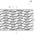

Classifications
-
- H01L23/14—
-
- C—CHEMISTRY; METALLURGY
- C08—ORGANIC MACROMOLECULAR COMPOUNDS; THEIR PREPARATION OR CHEMICAL WORKING-UP; COMPOSITIONS BASED THEREON
- C08J—WORKING-UP; GENERAL PROCESSES OF COMPOUNDING; AFTER-TREATMENT NOT COVERED BY SUBCLASSES C08B, C08C, C08F, C08G or C08H
- C08J5/00—Manufacture of articles or shaped materials containing macromolecular substances
- C08J5/24—Impregnating materials with prepolymers which can be polymerised in situ, e.g. manufacture of prepregs
- C08J5/241—Impregnating materials with prepolymers which can be polymerised in situ, e.g. manufacture of prepregs using inorganic fibres
- C08J5/244—Impregnating materials with prepolymers which can be polymerised in situ, e.g. manufacture of prepregs using inorganic fibres using glass fibres
-
- B—PERFORMING OPERATIONS; TRANSPORTING
- B32—LAYERED PRODUCTS
- B32B—LAYERED PRODUCTS, i.e. PRODUCTS BUILT-UP OF STRATA OF FLAT OR NON-FLAT, e.g. CELLULAR OR HONEYCOMB, FORM
- B32B15/00—Layered products comprising a layer of metal
- B32B15/04—Layered products comprising a layer of metal comprising metal as the main or only constituent of a layer, which is next to another layer of the same or of a different material
- B32B15/08—Layered products comprising a layer of metal comprising metal as the main or only constituent of a layer, which is next to another layer of the same or of a different material of synthetic resin
-
- B—PERFORMING OPERATIONS; TRANSPORTING
- B32—LAYERED PRODUCTS
- B32B—LAYERED PRODUCTS, i.e. PRODUCTS BUILT-UP OF STRATA OF FLAT OR NON-FLAT, e.g. CELLULAR OR HONEYCOMB, FORM
- B32B15/00—Layered products comprising a layer of metal
- B32B15/14—Layered products comprising a layer of metal next to a fibrous or filamentary layer
-
- B—PERFORMING OPERATIONS; TRANSPORTING
- B32—LAYERED PRODUCTS
- B32B—LAYERED PRODUCTS, i.e. PRODUCTS BUILT-UP OF STRATA OF FLAT OR NON-FLAT, e.g. CELLULAR OR HONEYCOMB, FORM
- B32B37/00—Methods or apparatus for laminating, e.g. by curing or by ultrasonic bonding
- B32B37/06—Methods or apparatus for laminating, e.g. by curing or by ultrasonic bonding characterised by the heating method
-
- B—PERFORMING OPERATIONS; TRANSPORTING
- B32—LAYERED PRODUCTS
- B32B—LAYERED PRODUCTS, i.e. PRODUCTS BUILT-UP OF STRATA OF FLAT OR NON-FLAT, e.g. CELLULAR OR HONEYCOMB, FORM
- B32B37/00—Methods or apparatus for laminating, e.g. by curing or by ultrasonic bonding
- B32B37/10—Methods or apparatus for laminating, e.g. by curing or by ultrasonic bonding characterised by the pressing technique, e.g. using action of vacuum or fluid pressure
-
- H—ELECTRICITY
- H05—ELECTRIC TECHNIQUES NOT OTHERWISE PROVIDED FOR
- H05K—PRINTED CIRCUITS; CASINGS OR CONSTRUCTIONAL DETAILS OF ELECTRIC APPARATUS; MANUFACTURE OF ASSEMBLAGES OF ELECTRICAL COMPONENTS
- H05K1/00—Printed circuits
- H05K1/02—Details
- H05K1/03—Use of materials for the substrate
-
- H—ELECTRICITY
- H10—SEMICONDUCTOR DEVICES; ELECTRIC SOLID-STATE DEVICES NOT OTHERWISE PROVIDED FOR
- H10W—GENERIC PACKAGES, INTERCONNECTIONS, CONNECTORS OR OTHER CONSTRUCTIONAL DETAILS OF DEVICES COVERED BY CLASS H10
- H10W70/00—Package substrates; Interposers; Redistribution layers [RDL]
- H10W70/01—Manufacture or treatment
- H10W70/05—Manufacture or treatment of insulating or insulated package substrates, or of interposers, or of redistribution layers
-
- H—ELECTRICITY
- H10—SEMICONDUCTOR DEVICES; ELECTRIC SOLID-STATE DEVICES NOT OTHERWISE PROVIDED FOR
- H10W—GENERIC PACKAGES, INTERCONNECTIONS, CONNECTORS OR OTHER CONSTRUCTIONAL DETAILS OF DEVICES COVERED BY CLASS H10
- H10W70/00—Package substrates; Interposers; Redistribution layers [RDL]
- H10W70/60—Insulating or insulated package substrates; Interposers; Redistribution layers
- H10W70/67—Insulating or insulated package substrates; Interposers; Redistribution layers characterised by their insulating layers or insulating parts
- H10W70/68—Shapes or dispositions thereof
- H10W70/685—Shapes or dispositions thereof comprising multiple insulating layers
-
- H—ELECTRICITY
- H10—SEMICONDUCTOR DEVICES; ELECTRIC SOLID-STATE DEVICES NOT OTHERWISE PROVIDED FOR
- H10W—GENERIC PACKAGES, INTERCONNECTIONS, CONNECTORS OR OTHER CONSTRUCTIONAL DETAILS OF DEVICES COVERED BY CLASS H10
- H10W70/00—Package substrates; Interposers; Redistribution layers [RDL]
- H10W70/60—Insulating or insulated package substrates; Interposers; Redistribution layers
- H10W70/67—Insulating or insulated package substrates; Interposers; Redistribution layers characterised by their insulating layers or insulating parts
- H10W70/69—Insulating materials thereof
-
- B—PERFORMING OPERATIONS; TRANSPORTING
- B32—LAYERED PRODUCTS
- B32B—LAYERED PRODUCTS, i.e. PRODUCTS BUILT-UP OF STRATA OF FLAT OR NON-FLAT, e.g. CELLULAR OR HONEYCOMB, FORM
- B32B2250/00—Layers arrangement
- B32B2250/40—Symmetrical or sandwich layers, e.g. ABA, ABCBA, ABCCBA
-
- B—PERFORMING OPERATIONS; TRANSPORTING
- B32—LAYERED PRODUCTS
- B32B—LAYERED PRODUCTS, i.e. PRODUCTS BUILT-UP OF STRATA OF FLAT OR NON-FLAT, e.g. CELLULAR OR HONEYCOMB, FORM
- B32B2260/00—Layered product comprising an impregnated, embedded, or bonded layer wherein the layer comprises an impregnation, embedding, or binder material
- B32B2260/02—Composition of the impregnated, bonded or embedded layer
- B32B2260/021—Fibrous or filamentary layer
-
- B—PERFORMING OPERATIONS; TRANSPORTING
- B32—LAYERED PRODUCTS
- B32B—LAYERED PRODUCTS, i.e. PRODUCTS BUILT-UP OF STRATA OF FLAT OR NON-FLAT, e.g. CELLULAR OR HONEYCOMB, FORM
- B32B2260/00—Layered product comprising an impregnated, embedded, or bonded layer wherein the layer comprises an impregnation, embedding, or binder material
- B32B2260/04—Impregnation, embedding, or binder material
- B32B2260/046—Synthetic resin
-
- B—PERFORMING OPERATIONS; TRANSPORTING
- B32—LAYERED PRODUCTS
- B32B—LAYERED PRODUCTS, i.e. PRODUCTS BUILT-UP OF STRATA OF FLAT OR NON-FLAT, e.g. CELLULAR OR HONEYCOMB, FORM
- B32B2305/00—Condition, form or state of the layers or laminate
- B32B2305/07—Parts immersed or impregnated in a matrix
- B32B2305/076—Prepregs
-
- B—PERFORMING OPERATIONS; TRANSPORTING
- B32—LAYERED PRODUCTS
- B32B—LAYERED PRODUCTS, i.e. PRODUCTS BUILT-UP OF STRATA OF FLAT OR NON-FLAT, e.g. CELLULAR OR HONEYCOMB, FORM
- B32B2307/00—Properties of the layers or laminate
- B32B2307/70—Other properties
- B32B2307/732—Dimensional properties
- B32B2307/737—Dimensions, e.g. volume or area
- B32B2307/7375—Linear, e.g. length, distance or width
- B32B2307/7376—Thickness
-
- B—PERFORMING OPERATIONS; TRANSPORTING
- B32—LAYERED PRODUCTS
- B32B—LAYERED PRODUCTS, i.e. PRODUCTS BUILT-UP OF STRATA OF FLAT OR NON-FLAT, e.g. CELLULAR OR HONEYCOMB, FORM
- B32B2457/00—Electrical equipment
-
- B—PERFORMING OPERATIONS; TRANSPORTING
- B32—LAYERED PRODUCTS
- B32B—LAYERED PRODUCTS, i.e. PRODUCTS BUILT-UP OF STRATA OF FLAT OR NON-FLAT, e.g. CELLULAR OR HONEYCOMB, FORM
- B32B2457/00—Electrical equipment
- B32B2457/08—PCBs, i.e. printed circuit boards
-
- C—CHEMISTRY; METALLURGY
- C08—ORGANIC MACROMOLECULAR COMPOUNDS; THEIR PREPARATION OR CHEMICAL WORKING-UP; COMPOSITIONS BASED THEREON
- C08J—WORKING-UP; GENERAL PROCESSES OF COMPOUNDING; AFTER-TREATMENT NOT COVERED BY SUBCLASSES C08B, C08C, C08F, C08G or C08H
- C08J2379/00—Characterised by the use of macromolecular compounds obtained by reactions forming in the main chain of the macromolecule a linkage containing nitrogen with or without oxygen, or carbon only, not provided for in groups C08J2361/00 - C08J2377/00
- C08J2379/04—Polycondensates having nitrogen-containing heterocyclic rings in the main chain; Polyhydrazides; Polyamide acids or similar polyimide precursors
- C08J2379/08—Polyimides; Polyester-imides; Polyamide-imides; Polyamide acids or similar polyimide precursors
-
- C—CHEMISTRY; METALLURGY
- C08—ORGANIC MACROMOLECULAR COMPOUNDS; THEIR PREPARATION OR CHEMICAL WORKING-UP; COMPOSITIONS BASED THEREON
- C08J—WORKING-UP; GENERAL PROCESSES OF COMPOUNDING; AFTER-TREATMENT NOT COVERED BY SUBCLASSES C08B, C08C, C08F, C08G or C08H
- C08J2463/00—Characterised by the use of epoxy resins; Derivatives of epoxy resins
-
- H—ELECTRICITY
- H10—SEMICONDUCTOR DEVICES; ELECTRIC SOLID-STATE DEVICES NOT OTHERWISE PROVIDED FOR
- H10W—GENERIC PACKAGES, INTERCONNECTIONS, CONNECTORS OR OTHER CONSTRUCTIONAL DETAILS OF DEVICES COVERED BY CLASS H10
- H10W70/00—Package substrates; Interposers; Redistribution layers [RDL]
- H10W70/60—Insulating or insulated package substrates; Interposers; Redistribution layers
- H10W70/67—Insulating or insulated package substrates; Interposers; Redistribution layers characterised by their insulating layers or insulating parts
- H10W70/69—Insulating materials thereof
- H10W70/695—Organic materials
Landscapes
- Chemical & Material Sciences (AREA)
- Engineering & Computer Science (AREA)
- Materials Engineering (AREA)
- Health & Medical Sciences (AREA)
- Microelectronics & Electronic Packaging (AREA)
- Inorganic Chemistry (AREA)
- Manufacturing & Machinery (AREA)
- Chemical Kinetics & Catalysis (AREA)
- Medicinal Chemistry (AREA)
- Polymers & Plastics (AREA)
- Organic Chemistry (AREA)
- Fluid Mechanics (AREA)
- Physics & Mathematics (AREA)
- Reinforced Plastic Materials (AREA)
- Laminated Bodies (AREA)
- Compositions Of Macromolecular Compounds (AREA)
Applications Claiming Priority (3)
| Application Number | Priority Date | Filing Date | Title |
|---|---|---|---|
| PCT/JP2020/035462 WO2022059167A1 (ja) | 2020-09-18 | 2020-09-18 | 半導体パッケージ用基板材料を製造する方法、プリプレグ、及び半導体パッケージ用基板材料 |
| JPPCT/JP2020/035462 | 2020-09-18 | ||
| PCT/JP2021/033973 WO2022059716A1 (ja) | 2020-09-18 | 2021-09-15 | 半導体パッケージ用基板材料を製造する方法、プリプレグ、及び半導体パッケージ用基板材料 |
Publications (1)
| Publication Number | Publication Date |
|---|---|
| KR20230058428A true KR20230058428A (ko) | 2023-05-03 |
Family
ID=80776026
Family Applications (1)
| Application Number | Title | Priority Date | Filing Date |
|---|---|---|---|
| KR1020237009217A Ceased KR20230058428A (ko) | 2020-09-18 | 2021-09-15 | 반도체 패키지용 기판 재료를 제조하는 방법, 프리프레그, 및 반도체 패키지용 기판 재료 |
Country Status (4)
| Country | Link |
|---|---|
| US (1) | US20230331946A1 (https=) |
| JP (2) | JP7239065B2 (https=) |
| KR (1) | KR20230058428A (https=) |
| WO (2) | WO2022059167A1 (https=) |
Families Citing this family (6)
| Publication number | Priority date | Publication date | Assignee | Title |
|---|---|---|---|---|
| WO2022059167A1 (ja) * | 2020-09-18 | 2022-03-24 | 昭和電工マテリアルズ株式会社 | 半導体パッケージ用基板材料を製造する方法、プリプレグ、及び半導体パッケージ用基板材料 |
| WO2023042305A1 (ja) * | 2021-09-15 | 2023-03-23 | 株式会社レゾナック | 半導体パッケージ用基板材料を製造する方法、プリプレグ、及びプリプレグの応用 |
| KR20250121006A (ko) * | 2022-12-07 | 2025-08-11 | 가부시끼가이샤 레조낙 | 금속장 적층판, 프린트 배선판 및 반도체 패키지 |
| CN120239650A (zh) * | 2022-12-07 | 2025-07-01 | 株式会社力森诺科 | 覆金属层叠板、印刷线路板及半导体封装体 |
| WO2025154213A1 (ja) * | 2024-01-17 | 2025-07-24 | 株式会社レゾナック | 半導体パッケージを製造する方法、半導体パッケージ用基板材料、及び半導体パッケージ用基板材料を製造する方法 |
| WO2025154212A1 (ja) * | 2024-01-17 | 2025-07-24 | 株式会社レゾナック | 半導体パッケージ用基板及びその製造方法、配線基板、並びに半導体パッケージ |
Citations (2)
| Publication number | Priority date | Publication date | Assignee | Title |
|---|---|---|---|---|
| JPH08198982A (ja) | 1995-01-24 | 1996-08-06 | Matsushita Electric Works Ltd | 積層板の製造方法 |
| JPH11126978A (ja) | 1997-10-24 | 1999-05-11 | Kyocera Corp | 多層配線基板 |
Family Cites Families (7)
| Publication number | Priority date | Publication date | Assignee | Title |
|---|---|---|---|---|
| JP2016050294A (ja) * | 2014-09-02 | 2016-04-11 | 日立化成株式会社 | 熱硬化性樹脂組成物、並びにこれを用いたプリプレグ、積層板及びプリント配線板 |
| JP6519128B2 (ja) * | 2014-09-19 | 2019-05-29 | 日立化成株式会社 | 熱硬化性樹脂組成物及びその製造方法、並びにこれを用いたプリプレグ、積層板及びプリント配線板 |
| JP6459343B2 (ja) * | 2014-09-26 | 2019-01-30 | パナソニックIpマネジメント株式会社 | プリプレグ、金属張積層板及びプリント配線板 |
| JP6606882B2 (ja) * | 2015-06-19 | 2019-11-20 | 日立化成株式会社 | 熱硬化性樹脂組成物、プリプレグ、積層板及び多層プリント配線板 |
| JP6911806B2 (ja) * | 2018-03-29 | 2021-07-28 | 味の素株式会社 | 樹脂組成物、シート状積層材料、プリント配線板及び半導体装置 |
| KR102672360B1 (ko) * | 2018-06-01 | 2024-06-04 | 미츠비시 가스 가가쿠 가부시키가이샤 | 수지 조성물, 프리프레그, 금속박 피복 적층판, 수지 시트 및 프린트 배선판 |
| WO2022059167A1 (ja) | 2020-09-18 | 2022-03-24 | 昭和電工マテリアルズ株式会社 | 半導体パッケージ用基板材料を製造する方法、プリプレグ、及び半導体パッケージ用基板材料 |
-
2020
- 2020-09-18 WO PCT/JP2020/035462 patent/WO2022059167A1/ja not_active Ceased
-
2021
- 2021-09-15 JP JP2022534621A patent/JP7239065B2/ja active Active
- 2021-09-15 KR KR1020237009217A patent/KR20230058428A/ko not_active Ceased
- 2021-09-15 US US18/245,347 patent/US20230331946A1/en active Pending
- 2021-09-15 WO PCT/JP2021/033973 patent/WO2022059716A1/ja not_active Ceased
-
2023
- 2023-03-01 JP JP2023031149A patent/JP7764871B2/ja active Active
Patent Citations (2)
| Publication number | Priority date | Publication date | Assignee | Title |
|---|---|---|---|---|
| JPH08198982A (ja) | 1995-01-24 | 1996-08-06 | Matsushita Electric Works Ltd | 積層板の製造方法 |
| JPH11126978A (ja) | 1997-10-24 | 1999-05-11 | Kyocera Corp | 多層配線基板 |
Also Published As
| Publication number | Publication date |
|---|---|
| TW202216868A (zh) | 2022-05-01 |
| JPWO2022059716A1 (https=) | 2022-03-24 |
| JP7764871B2 (ja) | 2025-11-06 |
| US20230331946A1 (en) | 2023-10-19 |
| JP7239065B2 (ja) | 2023-03-14 |
| JP2023081928A (ja) | 2023-06-13 |
| WO2022059716A1 (ja) | 2022-03-24 |
| WO2022059167A1 (ja) | 2022-03-24 |
Similar Documents
| Publication | Publication Date | Title |
|---|---|---|
| JP7239065B2 (ja) | 半導体パッケージ用基板材料を製造する方法、プリプレグ、及び半導体パッケージ用基板材料 | |
| JP7435712B2 (ja) | 樹脂組成物、半導体用配線層積層体及び半導体装置 | |
| KR101184527B1 (ko) | 감광성 접착제 조성물, 필름상 접착제, 접착 시트, 접착제 패턴의 형성방법, 접착제층 부착 반도체 웨이퍼, 반도체 장치, 및, 반도체 장치의 제조방법 | |
| JP6045772B2 (ja) | 感光性接着剤組成物、フィルム状接着剤、接着シート、接着剤パターン、接着剤層付半導体ウェハ、半導体装置、及び半導体装置の製造方法 | |
| US20100178501A1 (en) | Adhesive composition, film-like adhesive, adhesive sheet, and semiconductor device made with the same | |
| KR20120080634A (ko) | 반도체 장치, 반도체 장치의 제조 방법 및 접착제층 부착 반도체 웨이퍼 | |
| KR20120066672A (ko) | 접착제 조성물, 그것을 사용한 반도체 장치 및 그 제조 방법 | |
| JP5663826B2 (ja) | 接着シート、接着剤層付半導体ウェハ、並びに半導体装置及びその製造方法 | |
| WO2015008330A1 (ja) | 感光性樹脂組成物、フィルム状接着剤、接着シート、接着剤パターン、接着剤層付半導体ウェハ及び半導体装置 | |
| JP7794149B2 (ja) | 半導体パッケージ用基板材料を製造する方法、プリプレグ、及びプリプレグの応用 | |
| WO2022059711A1 (ja) | 有機コア材及びその製造方法、有機コア材を含む積層体、並びに配線板 | |
| JP2020095111A (ja) | 感光性樹脂組成物、並びにこれを用いた半導体用配線層及び半導体基板 | |
| WO2010032529A1 (ja) | 半導体装置及びその製造方法 | |
| KR20130046426A (ko) | 접착제층 부착 반도체 웨이퍼의 제조 방법, 감광성 접착제 및 반도체 장치 | |
| TWI918719B (zh) | 製造半導體封裝用基板材料之方法、預浸體及半導體封裝用基板材料 | |
| JP5263050B2 (ja) | 接着剤組成物及びそれを用いた半導体装置の製造方法、半導体装置 | |
| JP7447459B2 (ja) | 積層フィルム、配線基板を製造する方法、及び半導体装置を製造する方法 | |
| JP2016180929A (ja) | 感光性樹脂組成物、感光性フィルム、感光性シート、樹脂パターン、樹脂層付半導体ウェハ及び半導体装置。 | |
| TW202313809A (zh) | 製造半導體封裝用基板材料之方法、預浸體及預浸體的應用 | |
| JP5671778B2 (ja) | 半導体封止用フィルム状接着剤、半導体装置及びその製造方法 | |
| JP2009141008A (ja) | 半導体装置及びその製造方法、並びに、感光性接着フィルム |
Legal Events
| Date | Code | Title | Description |
|---|---|---|---|
| PA0105 | International application |
St.27 status event code: A-0-1-A10-A15-nap-PA0105 |
|
| PG1501 | Laying open of application |
St.27 status event code: A-1-1-Q10-Q12-nap-PG1501 |
|
| R18-X000 | Changes to party contact information recorded |
St.27 status event code: A-3-3-R10-R18-oth-X000 |
|
| A201 | Request for examination | ||
| PA0201 | Request for examination |
St.27 status event code: A-1-2-D10-D11-exm-PA0201 |
|
| E902 | Notification of reason for refusal | ||
| PE0902 | Notice of grounds for rejection |
St.27 status event code: A-1-2-D10-D21-exm-PE0902 |
|
| P11 | Amendment of application requested |
Free format text: ST27 STATUS EVENT CODE: A-2-2-P10-P11-NAP-X000 (AS PROVIDED BY THE NATIONAL OFFICE) |
|
| P11-X000 | Amendment of application requested |
St.27 status event code: A-2-2-P10-P11-nap-X000 |
|
| P13 | Application amended |
Free format text: ST27 STATUS EVENT CODE: A-2-2-P10-P13-NAP-X000 (AS PROVIDED BY THE NATIONAL OFFICE) |
|
| P13-X000 | Application amended |
St.27 status event code: A-2-2-P10-P13-nap-X000 |
|
| P22-X000 | Classification modified |
St.27 status event code: A-2-2-P10-P22-nap-X000 |
|
| B15 | Application refused following examination |
Free format text: ST27 STATUS EVENT CODE: N-2-6-B10-B15-EXM-PE0601 (AS PROVIDED BY THE NATIONAL OFFICE) |
|
| PE0601 | Decision on rejection of patent |
St.27 status event code: N-2-6-B10-B15-exm-PE0601 |