KR20150076260A - 광학 필름 - Google Patents
광학 필름 Download PDFInfo
- Publication number
- KR20150076260A KR20150076260A KR1020157015731A KR20157015731A KR20150076260A KR 20150076260 A KR20150076260 A KR 20150076260A KR 1020157015731 A KR1020157015731 A KR 1020157015731A KR 20157015731 A KR20157015731 A KR 20157015731A KR 20150076260 A KR20150076260 A KR 20150076260A
- Authority
- KR
- South Korea
- Prior art keywords
- cutting tool
- master
- prism
- film
- micrometers
- Prior art date
- Legal status (The legal status is an assumption and is not a legal conclusion. Google has not performed a legal analysis and makes no representation as to the accuracy of the status listed.)
- Ceased
Links
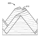
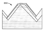
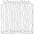
- 239000012788 optical film Substances 0.000 title abstract description 23
- 238000005520 cutting process Methods 0.000 abstract description 114
- 230000033001 locomotion Effects 0.000 abstract description 54
- 230000002265 prevention Effects 0.000 abstract description 19
- 238000000034 method Methods 0.000 abstract description 16
- 238000004519 manufacturing process Methods 0.000 abstract description 12
- 239000010408 film Substances 0.000 description 100
- 230000007547 defect Effects 0.000 description 16
- 238000007516 diamond turning Methods 0.000 description 10
- 230000007246 mechanism Effects 0.000 description 7
- 239000000463 material Substances 0.000 description 6
- 230000003287 optical effect Effects 0.000 description 6
- 238000013459 approach Methods 0.000 description 4
- NIXOWILDQLNWCW-UHFFFAOYSA-N acrylic acid group Chemical group C(C=C)(=O)O NIXOWILDQLNWCW-UHFFFAOYSA-N 0.000 description 3
- 230000000694 effects Effects 0.000 description 3
- 238000000605 extraction Methods 0.000 description 3
- 230000004048 modification Effects 0.000 description 3
- 238000012986 modification Methods 0.000 description 3
- 230000004044 response Effects 0.000 description 3
- 125000006850 spacer group Chemical group 0.000 description 3
- 239000000758 substrate Substances 0.000 description 3
- PXHVJJICTQNCMI-UHFFFAOYSA-N Nickel Chemical compound [Ni] PXHVJJICTQNCMI-UHFFFAOYSA-N 0.000 description 2
- 230000000712 assembly Effects 0.000 description 2
- 238000000429 assembly Methods 0.000 description 2
- 238000005266 casting Methods 0.000 description 2
- 230000008859 change Effects 0.000 description 2
- 238000009792 diffusion process Methods 0.000 description 2
- 238000005286 illumination Methods 0.000 description 2
- 238000007689 inspection Methods 0.000 description 2
- 239000004973 liquid crystal related substance Substances 0.000 description 2
- 239000011159 matrix material Substances 0.000 description 2
- 230000000737 periodic effect Effects 0.000 description 2
- 229920000139 polyethylene terephthalate Polymers 0.000 description 2
- 239000005020 polyethylene terephthalate Substances 0.000 description 2
- 230000001902 propagating effect Effects 0.000 description 2
- RYGMFSIKBFXOCR-UHFFFAOYSA-N Copper Chemical compound [Cu] RYGMFSIKBFXOCR-UHFFFAOYSA-N 0.000 description 1
- 229910000831 Steel Inorganic materials 0.000 description 1
- 230000009471 action Effects 0.000 description 1
- XAGFODPZIPBFFR-UHFFFAOYSA-N aluminium Chemical compound [Al] XAGFODPZIPBFFR-UHFFFAOYSA-N 0.000 description 1
- 229910052782 aluminium Inorganic materials 0.000 description 1
- 238000000149 argon plasma sintering Methods 0.000 description 1
- 230000009286 beneficial effect Effects 0.000 description 1
- 230000005540 biological transmission Effects 0.000 description 1
- 230000002860 competitive effect Effects 0.000 description 1
- 230000000295 complement effect Effects 0.000 description 1
- 238000010276 construction Methods 0.000 description 1
- 229910052802 copper Inorganic materials 0.000 description 1
- 239000010949 copper Substances 0.000 description 1
- 238000001723 curing Methods 0.000 description 1
- 230000000593 degrading effect Effects 0.000 description 1
- 230000001419 dependent effect Effects 0.000 description 1
- 238000010586 diagram Methods 0.000 description 1
- 229910003460 diamond Inorganic materials 0.000 description 1
- 239000010432 diamond Substances 0.000 description 1
- 230000009977 dual effect Effects 0.000 description 1
- 239000000428 dust Substances 0.000 description 1
- 230000008030 elimination Effects 0.000 description 1
- 238000003379 elimination reaction Methods 0.000 description 1
- 238000004049 embossing Methods 0.000 description 1
- 230000002708 enhancing effect Effects 0.000 description 1
- 238000001125 extrusion Methods 0.000 description 1
- 238000009434 installation Methods 0.000 description 1
- 230000001788 irregular Effects 0.000 description 1
- 230000007794 irritation Effects 0.000 description 1
- 238000001000 micrograph Methods 0.000 description 1
- 229910052759 nickel Inorganic materials 0.000 description 1
- 239000002245 particle Substances 0.000 description 1
- 230000010363 phase shift Effects 0.000 description 1
- 239000004033 plastic Substances 0.000 description 1
- 229920003023 plastic Polymers 0.000 description 1
- 230000010287 polarization Effects 0.000 description 1
- 229920000515 polycarbonate Polymers 0.000 description 1
- 239000004417 polycarbonate Substances 0.000 description 1
- 229920000728 polyester Polymers 0.000 description 1
- 239000011112 polyethylene naphthalate Substances 0.000 description 1
- -1 polyethylene terephthalate Polymers 0.000 description 1
- 230000003449 preventive effect Effects 0.000 description 1
- 230000008569 process Effects 0.000 description 1
- 238000003908 quality control method Methods 0.000 description 1
- 230000009467 reduction Effects 0.000 description 1
- 238000001878 scanning electron micrograph Methods 0.000 description 1
- 239000010959 steel Substances 0.000 description 1
- 230000001360 synchronised effect Effects 0.000 description 1
- 239000012780 transparent material Substances 0.000 description 1
Images


Classifications
-
- G—PHYSICS
- G02—OPTICS
- G02B—OPTICAL ELEMENTS, SYSTEMS OR APPARATUS
- G02B5/00—Optical elements other than lenses
- G02B5/04—Prisms
- G02B5/045—Prism arrays
-
- G—PHYSICS
- G02—OPTICS
- G02B—OPTICAL ELEMENTS, SYSTEMS OR APPARATUS
- G02B5/00—Optical elements other than lenses
- G02B5/02—Diffusing elements; Afocal elements
- G02B5/0205—Diffusing elements; Afocal elements characterised by the diffusing properties
- G02B5/021—Diffusing elements; Afocal elements characterised by the diffusing properties the diffusion taking place at the element's surface, e.g. by means of surface roughening or microprismatic structures
- G02B5/0221—Diffusing elements; Afocal elements characterised by the diffusing properties the diffusion taking place at the element's surface, e.g. by means of surface roughening or microprismatic structures the surface having an irregular structure
-
- B—PERFORMING OPERATIONS; TRANSPORTING
- B29—WORKING OF PLASTICS; WORKING OF SUBSTANCES IN A PLASTIC STATE IN GENERAL
- B29D—PRODUCING PARTICULAR ARTICLES FROM PLASTICS OR FROM SUBSTANCES IN A PLASTIC STATE
- B29D11/00—Producing optical elements, e.g. lenses or prisms
- B29D11/0074—Production of other optical elements not provided for in B29D11/00009- B29D11/0073
- B29D11/00798—Producing diffusers
-
- B—PERFORMING OPERATIONS; TRANSPORTING
- B26—HAND CUTTING TOOLS; CUTTING; SEVERING
- B26D—CUTTING; DETAILS COMMON TO MACHINES FOR PERFORATING, PUNCHING, CUTTING-OUT, STAMPING-OUT OR SEVERING
- B26D3/00—Cutting work characterised by the nature of the cut made; Apparatus therefor
- B26D3/06—Grooving involving removal of material from the surface of the work
-
- B—PERFORMING OPERATIONS; TRANSPORTING
- B29—WORKING OF PLASTICS; WORKING OF SUBSTANCES IN A PLASTIC STATE IN GENERAL
- B29C—SHAPING OR JOINING OF PLASTICS; SHAPING OF MATERIAL IN A PLASTIC STATE, NOT OTHERWISE PROVIDED FOR; AFTER-TREATMENT OF THE SHAPED PRODUCTS, e.g. REPAIRING
- B29C59/00—Surface shaping of articles, e.g. embossing; Apparatus therefor
- B29C59/002—Component parts, details or accessories; Auxiliary operations
-
- B—PERFORMING OPERATIONS; TRANSPORTING
- B29—WORKING OF PLASTICS; WORKING OF SUBSTANCES IN A PLASTIC STATE IN GENERAL
- B29C—SHAPING OR JOINING OF PLASTICS; SHAPING OF MATERIAL IN A PLASTIC STATE, NOT OTHERWISE PROVIDED FOR; AFTER-TREATMENT OF THE SHAPED PRODUCTS, e.g. REPAIRING
- B29C59/00—Surface shaping of articles, e.g. embossing; Apparatus therefor
- B29C59/16—Surface shaping of articles, e.g. embossing; Apparatus therefor by wave energy or particle radiation, e.g. infrared heating
-
- G—PHYSICS
- G02—OPTICS
- G02B—OPTICAL ELEMENTS, SYSTEMS OR APPARATUS
- G02B5/00—Optical elements other than lenses
- G02B5/02—Diffusing elements; Afocal elements
- G02B5/0205—Diffusing elements; Afocal elements characterised by the diffusing properties
- G02B5/021—Diffusing elements; Afocal elements characterised by the diffusing properties the diffusion taking place at the element's surface, e.g. by means of surface roughening or microprismatic structures
- G02B5/0231—Diffusing elements; Afocal elements characterised by the diffusing properties the diffusion taking place at the element's surface, e.g. by means of surface roughening or microprismatic structures the surface having microprismatic or micropyramidal shape
-
- G—PHYSICS
- G02—OPTICS
- G02B—OPTICAL ELEMENTS, SYSTEMS OR APPARATUS
- G02B5/00—Optical elements other than lenses
- G02B5/02—Diffusing elements; Afocal elements
- G02B5/0268—Diffusing elements; Afocal elements characterized by the fabrication or manufacturing method
-
- G—PHYSICS
- G02—OPTICS
- G02B—OPTICAL ELEMENTS, SYSTEMS OR APPARATUS
- G02B5/00—Optical elements other than lenses
- G02B5/02—Diffusing elements; Afocal elements
- G02B5/0273—Diffusing elements; Afocal elements characterized by the use
- G02B5/0278—Diffusing elements; Afocal elements characterized by the use used in transmission
-
- G—PHYSICS
- G02—OPTICS
- G02B—OPTICAL ELEMENTS, SYSTEMS OR APPARATUS
- G02B6/00—Light guides; Structural details of arrangements comprising light guides and other optical elements, e.g. couplings
- G02B6/0001—Light guides; Structural details of arrangements comprising light guides and other optical elements, e.g. couplings specially adapted for lighting devices or systems
- G02B6/0011—Light guides; Structural details of arrangements comprising light guides and other optical elements, e.g. couplings specially adapted for lighting devices or systems the light guides being planar or of plate-like form
- G02B6/0033—Means for improving the coupling-out of light from the light guide
- G02B6/0035—Means for improving the coupling-out of light from the light guide provided on the surface of the light guide or in the bulk of it
- G02B6/0038—Linear indentations or grooves, e.g. arc-shaped grooves or meandering grooves, extending over the full length or width of the light guide
-
- G—PHYSICS
- G02—OPTICS
- G02B—OPTICAL ELEMENTS, SYSTEMS OR APPARATUS
- G02B6/00—Light guides; Structural details of arrangements comprising light guides and other optical elements, e.g. couplings
- G02B6/0001—Light guides; Structural details of arrangements comprising light guides and other optical elements, e.g. couplings specially adapted for lighting devices or systems
- G02B6/0011—Light guides; Structural details of arrangements comprising light guides and other optical elements, e.g. couplings specially adapted for lighting devices or systems the light guides being planar or of plate-like form
- G02B6/0065—Manufacturing aspects; Material aspects
-
- Y—GENERAL TAGGING OF NEW TECHNOLOGICAL DEVELOPMENTS; GENERAL TAGGING OF CROSS-SECTIONAL TECHNOLOGIES SPANNING OVER SEVERAL SECTIONS OF THE IPC; TECHNICAL SUBJECTS COVERED BY FORMER USPC CROSS-REFERENCE ART COLLECTIONS [XRACs] AND DIGESTS
- Y10—TECHNICAL SUBJECTS COVERED BY FORMER USPC
- Y10T—TECHNICAL SUBJECTS COVERED BY FORMER US CLASSIFICATION
- Y10T83/00—Cutting
- Y10T83/02—Other than completely through work thickness
- Y10T83/0304—Grooving
Landscapes
- Physics & Mathematics (AREA)
- General Physics & Mathematics (AREA)
- Optics & Photonics (AREA)
- Engineering & Computer Science (AREA)
- Manufacturing & Machinery (AREA)
- Mechanical Engineering (AREA)
- Health & Medical Sciences (AREA)
- Ophthalmology & Optometry (AREA)
- Forests & Forestry (AREA)
- Life Sciences & Earth Sciences (AREA)
- Optical Elements Other Than Lenses (AREA)
- Shaping Of Tube Ends By Bending Or Straightening (AREA)
- Moulds For Moulding Plastics Or The Like (AREA)
- Numerical Control (AREA)
- Turning (AREA)
- Toxicology (AREA)
Applications Claiming Priority (3)
| Application Number | Priority Date | Filing Date | Title |
|---|---|---|---|
| US97424507P | 2007-09-21 | 2007-09-21 | |
| US60/974,245 | 2007-09-21 | ||
| PCT/US2008/071122 WO2009042286A1 (en) | 2007-09-21 | 2008-07-25 | Optical film |
Related Parent Applications (1)
| Application Number | Title | Priority Date | Filing Date |
|---|---|---|---|
| KR1020107008567A Division KR20100077168A (ko) | 2007-09-21 | 2008-07-25 | 광학 필름 |
Publications (1)
| Publication Number | Publication Date |
|---|---|
| KR20150076260A true KR20150076260A (ko) | 2015-07-06 |
Family
ID=40511780
Family Applications (2)
| Application Number | Title | Priority Date | Filing Date |
|---|---|---|---|
| KR1020157015731A Ceased KR20150076260A (ko) | 2007-09-21 | 2008-07-25 | 광학 필름 |
| KR1020107008567A Ceased KR20100077168A (ko) | 2007-09-21 | 2008-07-25 | 광학 필름 |
Family Applications After (1)
| Application Number | Title | Priority Date | Filing Date |
|---|---|---|---|
| KR1020107008567A Ceased KR20100077168A (ko) | 2007-09-21 | 2008-07-25 | 광학 필름 |
Country Status (7)
| Country | Link |
|---|---|
| US (2) | US8503082B2 (enExample) |
| EP (1) | EP2203301A4 (enExample) |
| JP (2) | JP5635403B2 (enExample) |
| KR (2) | KR20150076260A (enExample) |
| CN (1) | CN101835597B (enExample) |
| TW (1) | TWI532590B (enExample) |
| WO (1) | WO2009042286A1 (enExample) |
Families Citing this family (23)
| Publication number | Priority date | Publication date | Assignee | Title |
|---|---|---|---|---|
| US9733400B2 (en) * | 2005-06-09 | 2017-08-15 | Ubright Optronics Corporation | Light directing film |
| JP5283376B2 (ja) * | 2007-12-21 | 2013-09-04 | 三菱レイヨン株式会社 | プリズムシート成形用ロール金型製造方法 |
| WO2009146055A2 (en) * | 2008-04-02 | 2009-12-03 | 3M Innovative Properties Company | Methods and systems for fabricating optical films having superimposed features |
| TWI483013B (zh) | 2008-04-02 | 2015-05-01 | 3M Innovative Properties Co | 光導膜及其製造方法 |
| JP5277842B2 (ja) * | 2008-09-30 | 2013-08-28 | 王子ホールディングス株式会社 | 光拡散シート |
| US8899814B2 (en) * | 2009-02-26 | 2014-12-02 | Dai Nippon Printing Co., Ltd. | Optical sheet with unit prisms including unit prism groups |
| JP5477072B2 (ja) * | 2010-03-12 | 2014-04-23 | 大日本印刷株式会社 | 金型、金型の製造方法、プリズムシート、光学機能シート、光学フィルター及び映像表示装置 |
| US20160067931A1 (en) * | 2010-03-26 | 2016-03-10 | Ubright Optronics Corporation | Optical substrates having light collimating and diffusion structures |
| US9180609B2 (en) * | 2010-03-26 | 2015-11-10 | Ubright Optronics Corporation | Optical substrates having light collimating and diffusion structures |
| US10725330B2 (en) * | 2010-03-26 | 2020-07-28 | Ubright Optronics Corporation | Optical substrates having light collimating and diffusion structures |
| TWI458623B (zh) * | 2011-07-26 | 2014-11-01 | Benq Materials Corp | 用於製造相位差薄膜之滾輪的製造方法 |
| US10038356B2 (en) * | 2012-05-22 | 2018-07-31 | General Electric Company | Generator rotor refurbishing system and method of repairing a generator rotor |
| CN102789014A (zh) * | 2012-07-13 | 2012-11-21 | 北京康得新复合材料股份有限公司 | 一种增光膜和显示装置 |
| CN103630954A (zh) * | 2012-08-22 | 2014-03-12 | 友辉光电股份有限公司 | 光学膜、液晶显示器及液晶显示器的背光模块 |
| CN104871043B (zh) * | 2012-12-28 | 2017-09-26 | 旭硝子株式会社 | 光学元件、投影装置和光学元件的制造方法 |
| TWI494624B (zh) * | 2014-01-29 | 2015-08-01 | 群創光電股份有限公司 | 背光模組、包含其之顯示器及導光板之製備方法 |
| CN105388543B (zh) * | 2014-08-26 | 2018-12-14 | 友辉光电股份有限公司 | 在基板上形成凹凸结构的方法与模具制作的方法 |
| JP6169745B1 (ja) * | 2016-03-16 | 2017-07-26 | 株式会社マルヤテキスタイル | 3d模様付シート及びその製造方法 |
| TWI608457B (zh) * | 2016-05-04 | 2017-12-11 | 群創光電股份有限公司 | 顯示面板 |
| EP3774280B1 (en) * | 2018-03-29 | 2025-03-26 | 3M Innovative Properties Company | Method for making microfractured film |
| JP7337524B2 (ja) * | 2018-09-21 | 2023-09-04 | デクセリアルズ株式会社 | 微細加工装置、微細加工方法、転写型、及び転写物 |
| US11491672B2 (en) * | 2018-09-21 | 2022-11-08 | Dexerials Corporation | Microfabrication device, microfabrication method, transfer mold, and transfer object |
| US11624944B2 (en) * | 2020-07-29 | 2023-04-11 | Reald Spark, Llc | Backlight for switchable directional display |
Family Cites Families (30)
| Publication number | Priority date | Publication date | Assignee | Title |
|---|---|---|---|---|
| JP3128397B2 (ja) * | 1993-09-16 | 2001-01-29 | 株式会社クラレ | 積層体の製法 |
| DE69602588T2 (de) * | 1995-03-03 | 1999-10-14 | Minnesota Mining & Mfg | Lichtlenkender film mit in der höhe variierender strukturierter oberfläche und daraus hergestellter lichtlenkender artikel |
| US5919551A (en) * | 1996-04-12 | 1999-07-06 | 3M Innovative Properties Company | Variable pitch structured optical film |
| EP1057049B1 (en) * | 1998-02-18 | 2008-10-01 | Minnesota Mining And Manufacturing Company | Optical film |
| US6322236B1 (en) * | 1999-02-09 | 2001-11-27 | 3M Innovative Properties Company | Optical film with defect-reducing surface and method for making same |
| JP2001183642A (ja) * | 1999-12-24 | 2001-07-06 | Toppan Printing Co Ltd | マルチプリズムシート及びこれを用いた液晶表示装置 |
| US6862141B2 (en) * | 2002-05-20 | 2005-03-01 | General Electric Company | Optical substrate and method of making |
| US7180672B2 (en) * | 2002-05-20 | 2007-02-20 | General Electric Company | Optical substrate and method of making |
| US6952627B2 (en) * | 2002-12-18 | 2005-10-04 | General Electric Company | Method and apparatus for fabricating light management substrates |
| KR100432347B1 (ko) * | 2003-07-01 | 2004-05-20 | 주식회사 엘지에스 | 백라이트 유닛의 집광시트 |
| EP1694814A1 (en) | 2003-12-08 | 2006-08-30 | Covaris, Inc. | Apparatus and methods for sample preparation |
| US7072092B2 (en) * | 2003-12-31 | 2006-07-04 | General Electric Company | Optical substrate with modulated structure |
| US7106517B2 (en) * | 2003-12-31 | 2006-09-12 | General Electric Company | Display optical films |
| US7142767B2 (en) | 2003-12-31 | 2006-11-28 | 3M Innovative Properties Company | Scratch-resistant light directing films |
| KR20050092257A (ko) * | 2004-03-15 | 2005-09-21 | 엘지.필립스 엘시디 주식회사 | 프리즘 시트 및 그를 갖는 백라이트 유닛 |
| JP2005265894A (ja) * | 2004-03-16 | 2005-09-29 | Fuji Photo Film Co Ltd | 集光フィルタ |
| TW200600919A (en) * | 2004-06-22 | 2006-01-01 | Samsung Electronics Co Ltd | Optical film, backlight assembly and liquid crystal display device having the same |
| TWI304486B (en) * | 2006-10-19 | 2008-12-21 | Efun Technology Co Ltd | Brightness enhancement film having curved prism units and matte |
| US7203569B2 (en) * | 2004-08-31 | 2007-04-10 | General Electric Company | Machine tool control methods and designs for fabricating mesoscopic surface structures on substrates |
| US7278771B2 (en) * | 2004-11-22 | 2007-10-09 | 3M Innovative Properties Company | Optical film |
| JP2006235111A (ja) | 2005-02-23 | 2006-09-07 | General Electric Co <Ge> | 変調された構造体を有する光学基板 |
| US20060226583A1 (en) * | 2005-04-04 | 2006-10-12 | Marushin Patrick H | Light directing film |
| TWI351550B (en) * | 2005-06-09 | 2011-11-01 | Ubright Optronics Corp | Optical substrate |
| US20070019434A1 (en) * | 2005-07-22 | 2007-01-25 | Eastman Kodak Company | Turning film having variable pitch |
| US7418202B2 (en) * | 2005-08-04 | 2008-08-26 | 3M Innovative Properties Company | Article having a birefringent surface and microstructured features having a variable pitch or angles for use as a blur filter |
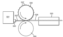
| US7293487B2 (en) | 2005-11-15 | 2007-11-13 | 3M Innovative Properties Company | Cutting tool having variable and independent movement in an x-direction and a z-direction into and laterally along a work piece for making microstructures |
| US7328638B2 (en) * | 2005-12-27 | 2008-02-12 | 3M Innovative Properties Company | Cutting tool using interrupted cut fast tool servo |
| TWI317025B (en) * | 2006-08-28 | 2009-11-11 | Eternal Chemical Co Ltd | Optical film |
| KR100936715B1 (ko) | 2007-03-16 | 2010-01-13 | 엘지전자 주식회사 | 광학필름 및 이를 포함하는 디스플레이 장치 |
| KR100905241B1 (ko) | 2007-04-13 | 2009-07-01 | 엘지전자 주식회사 | 복수의 구조체를 포함하는 광학 필름 및 이를 포함하는백라이트 유닛 |
-
2008
- 2008-07-25 US US12/678,676 patent/US8503082B2/en not_active Expired - Fee Related
- 2008-07-25 WO PCT/US2008/071122 patent/WO2009042286A1/en not_active Ceased
- 2008-07-25 CN CN2008801123656A patent/CN101835597B/zh not_active Expired - Fee Related
- 2008-07-25 KR KR1020157015731A patent/KR20150076260A/ko not_active Ceased
- 2008-07-25 JP JP2010525862A patent/JP5635403B2/ja not_active Expired - Fee Related
- 2008-07-25 EP EP08796595.0A patent/EP2203301A4/en not_active Withdrawn
- 2008-07-25 KR KR1020107008567A patent/KR20100077168A/ko not_active Ceased
- 2008-08-11 TW TW097130563A patent/TWI532590B/zh not_active IP Right Cessation
-
2013
- 2013-07-16 US US13/943,091 patent/US8885256B2/en active Active
-
2014
- 2014-10-16 JP JP2014211631A patent/JP6050299B2/ja not_active Expired - Fee Related
Also Published As
| Publication number | Publication date |
|---|---|
| JP6050299B2 (ja) | 2016-12-21 |
| WO2009042286A1 (en) | 2009-04-02 |
| KR20100077168A (ko) | 2010-07-07 |
| CN101835597B (zh) | 2013-05-22 |
| EP2203301A1 (en) | 2010-07-07 |
| CN101835597A (zh) | 2010-09-15 |
| JP2010540271A (ja) | 2010-12-24 |
| US8885256B2 (en) | 2014-11-11 |
| JP5635403B2 (ja) | 2014-12-03 |
| US8503082B2 (en) | 2013-08-06 |
| TW200914253A (en) | 2009-04-01 |
| US20110032623A1 (en) | 2011-02-10 |
| EP2203301A4 (en) | 2014-04-23 |
| JP2015071303A (ja) | 2015-04-16 |
| US20130301150A1 (en) | 2013-11-14 |
| TWI532590B (zh) | 2016-05-11 |
Similar Documents
| Publication | Publication Date | Title |
|---|---|---|
| US8503082B2 (en) | Optical film | |
| CN1161250C (zh) | 带减缺陷表面的光学薄膜及其制作方法 | |
| JP5873130B2 (ja) | 導光フィルム及び導光フィルムを製作するための方法 | |
| US8749722B2 (en) | Display device displaying an image for a first viewpoint and an image for a second viewpoint | |
| KR101280187B1 (ko) | 렌즈 시트, 면광원 장치 및 액정 표시 장치 | |
| KR20120026570A (ko) | 광 방향 전환 필름 및 이 필름을 사용한 디스플레이 | |
| US20080024870A1 (en) | Light-redirecting film containing optical modification layer | |
| CN101276101A (zh) | 具有可变厚度的光再定向膜 | |
| JP2008287221A (ja) | 不連続コーティングを有する光方向転換フィルム | |
| CN101061416A (zh) | 二维和三维视图显示器 | |
| JP2013077473A (ja) | 導光板、導光板の製造方法、金型、ディスプレイ用バックライトユニットおよびディスプレイ | |
| KR20090130430A (ko) | 액정 표시 장치, 면광원 장치 및 프리즘 시트, 및 이것들의 제조 방법 | |
| JP2011013430A (ja) | プリズムシートおよび該プリズムシートを用いた面光源装置 | |
| JP2012074308A (ja) | 光源ユニットおよび液晶表示装置 | |
| JP2008090324A (ja) | 液晶ディスプレイ用光拡散シート | |
| JP2011137856A (ja) | 直下型led光源バックライト用拡散シート | |
| JP2004102088A (ja) | 光学フィルムの製造方法及び液晶表示装置 | |
| MXPA01007967A (es) | Pelicula optica con superficie reductora de defectos y metodo para hacer la misma |
Legal Events
| Date | Code | Title | Description |
|---|---|---|---|
| A107 | Divisional application of patent | ||
| PA0104 | Divisional application for international application |
Comment text: Divisional Application for International Patent Patent event code: PA01041R01D Patent event date: 20150612 Application number text: 1020107008567 Filing date: 20100420 |
|
| PG1501 | Laying open of application | ||
| A201 | Request for examination | ||
| PA0201 | Request for examination |
Patent event code: PA02012R01D Patent event date: 20150713 Comment text: Request for Examination of Application |
|
| E902 | Notification of reason for refusal | ||
| PE0902 | Notice of grounds for rejection |
Comment text: Notification of reason for refusal Patent event date: 20150723 Patent event code: PE09021S01D |
|
| AMND | Amendment | ||
| E90F | Notification of reason for final refusal | ||
| PE0902 | Notice of grounds for rejection |
Comment text: Final Notice of Reason for Refusal Patent event date: 20160329 Patent event code: PE09021S02D |
|
| AMND | Amendment | ||
| E601 | Decision to refuse application | ||
| PE0601 | Decision on rejection of patent |
Patent event date: 20161020 Comment text: Decision to Refuse Application Patent event code: PE06012S01D Patent event date: 20160329 Comment text: Final Notice of Reason for Refusal Patent event code: PE06011S02I Patent event date: 20150723 Comment text: Notification of reason for refusal Patent event code: PE06011S01I |
|
| AMND | Amendment | ||
| J201 | Request for trial against refusal decision | ||
| PJ0201 | Trial against decision of rejection |
Patent event date: 20170119 Comment text: Request for Trial against Decision on Refusal Patent event code: PJ02012R01D Patent event date: 20161020 Comment text: Decision to Refuse Application Patent event code: PJ02011S01I Appeal kind category: Appeal against decision to decline refusal Appeal identifier: 2017101000295 Request date: 20170119 |
|
| PB0901 | Examination by re-examination before a trial |
Comment text: Amendment to Specification, etc. Patent event date: 20170119 Patent event code: PB09011R02I Comment text: Request for Trial against Decision on Refusal Patent event date: 20170119 Patent event code: PB09011R01I Comment text: Amendment to Specification, etc. Patent event date: 20160530 Patent event code: PB09011R02I Comment text: Amendment to Specification, etc. Patent event date: 20151023 Patent event code: PB09011R02I |
|
| E801 | Decision on dismissal of amendment | ||
| PE0801 | Dismissal of amendment |
Patent event code: PE08012E01D Comment text: Decision on Dismissal of Amendment Patent event date: 20170317 Patent event code: PE08011R01I Comment text: Amendment to Specification, etc. Patent event date: 20170119 Patent event code: PE08011R01I Comment text: Amendment to Specification, etc. Patent event date: 20160530 Patent event code: PE08011R01I Comment text: Amendment to Specification, etc. Patent event date: 20151023 |
|
| B601 | Maintenance of original decision after re-examination before a trial | ||
| PB0601 | Maintenance of original decision after re-examination before a trial | ||
| J301 | Trial decision |
Free format text: TRIAL NUMBER: 2017101000295; TRIAL DECISION FOR APPEAL AGAINST DECISION TO DECLINE REFUSAL REQUESTED 20170119 Effective date: 20180928 |
|
| PJ1301 | Trial decision |
Patent event code: PJ13011S01D Patent event date: 20180928 Comment text: Trial Decision on Objection to Decision on Refusal Appeal kind category: Appeal against decision to decline refusal Request date: 20170119 Decision date: 20180928 Appeal identifier: 2017101000295 |