KR20120095411A - 반도체 식각 방법 - Google Patents
반도체 식각 방법 Download PDFInfo
- Publication number
- KR20120095411A KR20120095411A KR1020127014823A KR20127014823A KR20120095411A KR 20120095411 A KR20120095411 A KR 20120095411A KR 1020127014823 A KR1020127014823 A KR 1020127014823A KR 20127014823 A KR20127014823 A KR 20127014823A KR 20120095411 A KR20120095411 A KR 20120095411A
- Authority
- KR
- South Korea
- Prior art keywords
- semiconductor
- etching
- etched
- photoresist
- reactive
- Prior art date
Links
- 239000004065 semiconductor Substances 0.000 title claims abstract description 131
- 238000000034 method Methods 0.000 title claims abstract description 57
- 238000005530 etching Methods 0.000 title claims abstract description 55
- 230000008569 process Effects 0.000 title description 5
- 229920002120 photoresistant polymer Polymers 0.000 claims abstract description 52
- 239000000463 material Substances 0.000 claims abstract description 34
- 238000000992 sputter etching Methods 0.000 claims abstract description 14
- 238000004140 cleaning Methods 0.000 claims abstract description 8
- 239000007789 gas Substances 0.000 claims description 32
- XKRFYHLGVUSROY-UHFFFAOYSA-N Argon Chemical compound [Ar] XKRFYHLGVUSROY-UHFFFAOYSA-N 0.000 claims description 16
- 239000000460 chlorine Substances 0.000 claims description 15
- IJGRMHOSHXDMSA-UHFFFAOYSA-N Atomic nitrogen Chemical compound N#N IJGRMHOSHXDMSA-UHFFFAOYSA-N 0.000 claims description 10
- 229910052786 argon Inorganic materials 0.000 claims description 8
- 230000005693 optoelectronics Effects 0.000 claims description 7
- 229910052793 cadmium Inorganic materials 0.000 claims description 6
- 229910052801 chlorine Inorganic materials 0.000 claims description 6
- ZAMOUSCENKQFHK-UHFFFAOYSA-N Chlorine atom Chemical compound [Cl] ZAMOUSCENKQFHK-UHFFFAOYSA-N 0.000 claims description 5
- BDOSMKKIYDKNTQ-UHFFFAOYSA-N cadmium atom Chemical compound [Cd] BDOSMKKIYDKNTQ-UHFFFAOYSA-N 0.000 claims description 5
- 229910052757 nitrogen Inorganic materials 0.000 claims description 5
- 229910052734 helium Inorganic materials 0.000 claims description 4
- FYYHWMGAXLPEAU-UHFFFAOYSA-N Magnesium Chemical compound [Mg] FYYHWMGAXLPEAU-UHFFFAOYSA-N 0.000 claims description 3
- BUGBHKTXTAQXES-UHFFFAOYSA-N Selenium Chemical compound [Se] BUGBHKTXTAQXES-UHFFFAOYSA-N 0.000 claims description 3
- HCHKCACWOHOZIP-UHFFFAOYSA-N Zinc Chemical compound [Zn] HCHKCACWOHOZIP-UHFFFAOYSA-N 0.000 claims description 3
- 229910045601 alloy Inorganic materials 0.000 claims description 3
- 239000000956 alloy Substances 0.000 claims description 3
- 239000001307 helium Substances 0.000 claims description 3
- SWQJXJOGLNCZEY-UHFFFAOYSA-N helium atom Chemical compound [He] SWQJXJOGLNCZEY-UHFFFAOYSA-N 0.000 claims description 3
- 229910052743 krypton Inorganic materials 0.000 claims description 3
- DNNSSWSSYDEUBZ-UHFFFAOYSA-N krypton atom Chemical compound [Kr] DNNSSWSSYDEUBZ-UHFFFAOYSA-N 0.000 claims description 3
- 229910052749 magnesium Inorganic materials 0.000 claims description 3
- 239000011777 magnesium Substances 0.000 claims description 3
- 229910052711 selenium Inorganic materials 0.000 claims description 3
- 239000011669 selenium Substances 0.000 claims description 3
- 229910052714 tellurium Inorganic materials 0.000 claims description 3
- PORWMNRCUJJQNO-UHFFFAOYSA-N tellurium atom Chemical compound [Te] PORWMNRCUJJQNO-UHFFFAOYSA-N 0.000 claims description 3
- 229910052724 xenon Inorganic materials 0.000 claims description 3
- FHNFHKCVQCLJFQ-UHFFFAOYSA-N xenon atom Chemical compound [Xe] FHNFHKCVQCLJFQ-UHFFFAOYSA-N 0.000 claims description 3
- 229910052725 zinc Inorganic materials 0.000 claims description 3
- 239000011701 zinc Substances 0.000 claims description 3
- 229910052754 neon Inorganic materials 0.000 claims description 2
- GKAOGPIIYCISHV-UHFFFAOYSA-N neon atom Chemical compound [Ne] GKAOGPIIYCISHV-UHFFFAOYSA-N 0.000 claims description 2
- 238000000605 extraction Methods 0.000 abstract description 12
- 238000001020 plasma etching Methods 0.000 description 19
- 239000000758 substrate Substances 0.000 description 17
- 150000002500 ions Chemical class 0.000 description 10
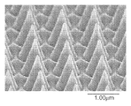
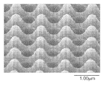
- 238000001878 scanning electron micrograph Methods 0.000 description 6
- -1 Si 3 N 4 Inorganic materials 0.000 description 5
- 238000005424 photoluminescence Methods 0.000 description 5
- 239000006096 absorbing agent Substances 0.000 description 4
- 238000001312 dry etching Methods 0.000 description 4
- 239000000203 mixture Substances 0.000 description 4
- XUIMIQQOPSSXEZ-UHFFFAOYSA-N Silicon Chemical compound [Si] XUIMIQQOPSSXEZ-UHFFFAOYSA-N 0.000 description 3
- 239000006227 byproduct Substances 0.000 description 3
- 238000009616 inductively coupled plasma Methods 0.000 description 3
- 229910052710 silicon Inorganic materials 0.000 description 3
- 239000010703 silicon Substances 0.000 description 3
- 238000003631 wet chemical etching Methods 0.000 description 3
- 206010073306 Exposure to radiation Diseases 0.000 description 2
- 229910004298 SiO 2 Inorganic materials 0.000 description 2
- NINIDFKCEFEMDL-UHFFFAOYSA-N Sulfur Chemical compound [S] NINIDFKCEFEMDL-UHFFFAOYSA-N 0.000 description 2
- QVGXLLKOCUKJST-UHFFFAOYSA-N atomic oxygen Chemical compound [O] QVGXLLKOCUKJST-UHFFFAOYSA-N 0.000 description 2
- 230000000052 comparative effect Effects 0.000 description 2
- 238000001918 dark-field optical micrograph Methods 0.000 description 2
- 238000000354 decomposition reaction Methods 0.000 description 2
- 238000010586 diagram Methods 0.000 description 2
- 239000012776 electronic material Substances 0.000 description 2
- 238000005259 measurement Methods 0.000 description 2
- 229910052751 metal Inorganic materials 0.000 description 2
- 239000002184 metal Substances 0.000 description 2
- 150000002739 metals Chemical class 0.000 description 2
- 239000001301 oxygen Substances 0.000 description 2
- 229910052760 oxygen Inorganic materials 0.000 description 2
- 238000000206 photolithography Methods 0.000 description 2
- 229920000642 polymer Polymers 0.000 description 2
- 238000004544 sputter deposition Methods 0.000 description 2
- 229910052717 sulfur Inorganic materials 0.000 description 2
- 239000011593 sulfur Substances 0.000 description 2
- 238000001039 wet etching Methods 0.000 description 2
- VXEGSRKPIUDPQT-UHFFFAOYSA-N 4-[4-(4-methoxyphenyl)piperazin-1-yl]aniline Chemical compound C1=CC(OC)=CC=C1N1CCN(C=2C=CC(N)=CC=2)CC1 VXEGSRKPIUDPQT-UHFFFAOYSA-N 0.000 description 1
- 229910000980 Aluminium gallium arsenide Inorganic materials 0.000 description 1
- 101001053401 Arabidopsis thaliana Acid beta-fructofuranosidase 3, vacuolar Proteins 0.000 description 1
- 229910014265 BrCl Inorganic materials 0.000 description 1
- KZBUYRJDOAKODT-UHFFFAOYSA-N Chlorine Chemical compound ClCl KZBUYRJDOAKODT-UHFFFAOYSA-N 0.000 description 1
- GYHNNYVSQQEPJS-UHFFFAOYSA-N Gallium Chemical compound [Ga] GYHNNYVSQQEPJS-UHFFFAOYSA-N 0.000 description 1
- 229910001218 Gallium arsenide Inorganic materials 0.000 description 1
- UFHFLCQGNIYNRP-UHFFFAOYSA-N Hydrogen Chemical compound [H][H] UFHFLCQGNIYNRP-UHFFFAOYSA-N 0.000 description 1
- 229910000661 Mercury cadmium telluride Inorganic materials 0.000 description 1
- OAICVXFJPJFONN-UHFFFAOYSA-N Phosphorus Chemical compound [P] OAICVXFJPJFONN-UHFFFAOYSA-N 0.000 description 1
- 229910003902 SiCl 4 Inorganic materials 0.000 description 1
- RTAQQCXQSZGOHL-UHFFFAOYSA-N Titanium Chemical compound [Ti] RTAQQCXQSZGOHL-UHFFFAOYSA-N 0.000 description 1
- 229910007709 ZnTe Inorganic materials 0.000 description 1
- 230000004075 alteration Effects 0.000 description 1
- 229910052782 aluminium Inorganic materials 0.000 description 1
- XAGFODPZIPBFFR-UHFFFAOYSA-N aluminium Chemical compound [Al] XAGFODPZIPBFFR-UHFFFAOYSA-N 0.000 description 1
- 229910052787 antimony Inorganic materials 0.000 description 1
- WATWJIUSRGPENY-UHFFFAOYSA-N antimony atom Chemical compound [Sb] WATWJIUSRGPENY-UHFFFAOYSA-N 0.000 description 1
- 229910052785 arsenic Inorganic materials 0.000 description 1
- RQNWIZPPADIBDY-UHFFFAOYSA-N arsenic atom Chemical compound [As] RQNWIZPPADIBDY-UHFFFAOYSA-N 0.000 description 1
- 230000015572 biosynthetic process Effects 0.000 description 1
- CODNYICXDISAEA-UHFFFAOYSA-N bromine monochloride Chemical compound BrCl CODNYICXDISAEA-UHFFFAOYSA-N 0.000 description 1
- 239000000969 carrier Substances 0.000 description 1
- 239000007795 chemical reaction product Substances 0.000 description 1
- 239000003795 chemical substances by application Substances 0.000 description 1
- 238000002508 contact lithography Methods 0.000 description 1
- 238000001816 cooling Methods 0.000 description 1
- 238000005260 corrosion Methods 0.000 description 1
- 230000007797 corrosion Effects 0.000 description 1
- 238000004132 cross linking Methods 0.000 description 1
- 230000003247 decreasing effect Effects 0.000 description 1
- 238000000151 deposition Methods 0.000 description 1
- 230000008021 deposition Effects 0.000 description 1
- 230000005684 electric field Effects 0.000 description 1
- 239000012634 fragment Substances 0.000 description 1
- 229910052733 gallium Inorganic materials 0.000 description 1
- 239000001257 hydrogen Substances 0.000 description 1
- 229910052739 hydrogen Inorganic materials 0.000 description 1
- 230000003116 impacting effect Effects 0.000 description 1
- 229910052738 indium Inorganic materials 0.000 description 1
- APFVFJFRJDLVQX-UHFFFAOYSA-N indium atom Chemical compound [In] APFVFJFRJDLVQX-UHFFFAOYSA-N 0.000 description 1
- 239000011261 inert gas Substances 0.000 description 1
- 230000003993 interaction Effects 0.000 description 1
- 238000000025 interference lithography Methods 0.000 description 1
- 238000001459 lithography Methods 0.000 description 1
- 238000004519 manufacturing process Methods 0.000 description 1
- 230000007246 mechanism Effects 0.000 description 1
- 238000001000 micrograph Methods 0.000 description 1
- 238000012986 modification Methods 0.000 description 1
- 230000004048 modification Effects 0.000 description 1
- 238000001451 molecular beam epitaxy Methods 0.000 description 1
- 239000002086 nanomaterial Substances 0.000 description 1
- 238000000059 patterning Methods 0.000 description 1
- 230000002085 persistent effect Effects 0.000 description 1
- 229910052698 phosphorus Inorganic materials 0.000 description 1
- 239000011574 phosphorus Substances 0.000 description 1
- 230000000704 physical effect Effects 0.000 description 1
- 239000000047 product Substances 0.000 description 1
- 230000000750 progressive effect Effects 0.000 description 1
- 238000005086 pumping Methods 0.000 description 1
- 239000000376 reactant Substances 0.000 description 1
- 230000004044 response Effects 0.000 description 1
- SBIBMFFZSBJNJF-UHFFFAOYSA-N selenium;zinc Chemical compound [Se]=[Zn] SBIBMFFZSBJNJF-UHFFFAOYSA-N 0.000 description 1
- 239000005049 silicon tetrachloride Substances 0.000 description 1
- 239000002210 silicon-based material Substances 0.000 description 1
- 229910052719 titanium Inorganic materials 0.000 description 1
- 239000010936 titanium Substances 0.000 description 1
- 231100000331 toxic Toxicity 0.000 description 1
- 230000002588 toxic effect Effects 0.000 description 1
- FAQYAMRNWDIXMY-UHFFFAOYSA-N trichloroborane Chemical compound ClB(Cl)Cl FAQYAMRNWDIXMY-UHFFFAOYSA-N 0.000 description 1
- WFKWXMTUELFFGS-UHFFFAOYSA-N tungsten Chemical compound [W] WFKWXMTUELFFGS-UHFFFAOYSA-N 0.000 description 1
- 229910052721 tungsten Inorganic materials 0.000 description 1
- 239000010937 tungsten Substances 0.000 description 1
Images


Classifications
-
- H—ELECTRICITY
- H01—ELECTRIC ELEMENTS
- H01L—SEMICONDUCTOR DEVICES NOT COVERED BY CLASS H10
- H01L21/00—Processes or apparatus adapted for the manufacture or treatment of semiconductor or solid state devices or of parts thereof
- H01L21/02—Manufacture or treatment of semiconductor devices or of parts thereof
- H01L21/04—Manufacture or treatment of semiconductor devices or of parts thereof the devices having at least one potential-jump barrier or surface barrier, e.g. PN junction, depletion layer or carrier concentration layer
- H01L21/18—Manufacture or treatment of semiconductor devices or of parts thereof the devices having at least one potential-jump barrier or surface barrier, e.g. PN junction, depletion layer or carrier concentration layer the devices having semiconductor bodies comprising elements of Group IV of the Periodic System or AIIIBV compounds with or without impurities, e.g. doping materials
- H01L21/30—Treatment of semiconductor bodies using processes or apparatus not provided for in groups H01L21/20 - H01L21/26
- H01L21/302—Treatment of semiconductor bodies using processes or apparatus not provided for in groups H01L21/20 - H01L21/26 to change their surface-physical characteristics or shape, e.g. etching, polishing, cutting
- H01L21/306—Chemical or electrical treatment, e.g. electrolytic etching
- H01L21/3065—Plasma etching; Reactive-ion etching
-
- H—ELECTRICITY
- H01—ELECTRIC ELEMENTS
- H01L—SEMICONDUCTOR DEVICES NOT COVERED BY CLASS H10
- H01L31/00—Semiconductor devices sensitive to infrared radiation, light, electromagnetic radiation of shorter wavelength or corpuscular radiation and specially adapted either for the conversion of the energy of such radiation into electrical energy or for the control of electrical energy by such radiation; Processes or apparatus specially adapted for the manufacture or treatment thereof or of parts thereof; Details thereof
- H01L31/02—Details
- H01L31/0236—Special surface textures
- H01L31/02363—Special surface textures of the semiconductor body itself, e.g. textured active layers
-
- H—ELECTRICITY
- H01—ELECTRIC ELEMENTS
- H01L—SEMICONDUCTOR DEVICES NOT COVERED BY CLASS H10
- H01L21/00—Processes or apparatus adapted for the manufacture or treatment of semiconductor or solid state devices or of parts thereof
- H01L21/02—Manufacture or treatment of semiconductor devices or of parts thereof
- H01L21/04—Manufacture or treatment of semiconductor devices or of parts thereof the devices having at least one potential-jump barrier or surface barrier, e.g. PN junction, depletion layer or carrier concentration layer
- H01L21/34—Manufacture or treatment of semiconductor devices or of parts thereof the devices having at least one potential-jump barrier or surface barrier, e.g. PN junction, depletion layer or carrier concentration layer the devices having semiconductor bodies not provided for in groups H01L21/0405, H01L21/0445, H01L21/06, H01L21/16 and H01L21/18 with or without impurities, e.g. doping materials
- H01L21/46—Treatment of semiconductor bodies using processes or apparatus not provided for in groups H01L21/428
- H01L21/461—Treatment of semiconductor bodies using processes or apparatus not provided for in groups H01L21/428 to change their surface-physical characteristics or shape, e.g. etching, polishing, cutting
- H01L21/465—Chemical or electrical treatment, e.g. electrolytic etching
-
- H—ELECTRICITY
- H01—ELECTRIC ELEMENTS
- H01L—SEMICONDUCTOR DEVICES NOT COVERED BY CLASS H10
- H01L2933/00—Details relating to devices covered by the group H01L33/00 but not provided for in its subgroups
- H01L2933/0083—Periodic patterns for optical field-shaping in or on the semiconductor body or semiconductor body package, e.g. photonic bandgap structures
-
- H—ELECTRICITY
- H01—ELECTRIC ELEMENTS
- H01L—SEMICONDUCTOR DEVICES NOT COVERED BY CLASS H10
- H01L33/00—Semiconductor devices with at least one potential-jump barrier or surface barrier specially adapted for light emission; Processes or apparatus specially adapted for the manufacture or treatment thereof or of parts thereof; Details thereof
- H01L33/005—Processes
- H01L33/0095—Post-treatment of devices, e.g. annealing, recrystallisation or short-circuit elimination
-
- H—ELECTRICITY
- H01—ELECTRIC ELEMENTS
- H01L—SEMICONDUCTOR DEVICES NOT COVERED BY CLASS H10
- H01L33/00—Semiconductor devices with at least one potential-jump barrier or surface barrier specially adapted for light emission; Processes or apparatus specially adapted for the manufacture or treatment thereof or of parts thereof; Details thereof
- H01L33/02—Semiconductor devices with at least one potential-jump barrier or surface barrier specially adapted for light emission; Processes or apparatus specially adapted for the manufacture or treatment thereof or of parts thereof; Details thereof characterised by the semiconductor bodies
- H01L33/20—Semiconductor devices with at least one potential-jump barrier or surface barrier specially adapted for light emission; Processes or apparatus specially adapted for the manufacture or treatment thereof or of parts thereof; Details thereof characterised by the semiconductor bodies with a particular shape, e.g. curved or truncated substrate
- H01L33/22—Roughened surfaces, e.g. at the interface between epitaxial layers
-
- Y—GENERAL TAGGING OF NEW TECHNOLOGICAL DEVELOPMENTS; GENERAL TAGGING OF CROSS-SECTIONAL TECHNOLOGIES SPANNING OVER SEVERAL SECTIONS OF THE IPC; TECHNICAL SUBJECTS COVERED BY FORMER USPC CROSS-REFERENCE ART COLLECTIONS [XRACs] AND DIGESTS
- Y02—TECHNOLOGIES OR APPLICATIONS FOR MITIGATION OR ADAPTATION AGAINST CLIMATE CHANGE
- Y02E—REDUCTION OF GREENHOUSE GAS [GHG] EMISSIONS, RELATED TO ENERGY GENERATION, TRANSMISSION OR DISTRIBUTION
- Y02E10/00—Energy generation through renewable energy sources
- Y02E10/50—Photovoltaic [PV] energy
Applications Claiming Priority (2)
| Application Number | Priority Date | Filing Date | Title |
|---|---|---|---|
| US25929909P | 2009-11-09 | 2009-11-09 | |
| US61/259,299 | 2009-11-09 |
Publications (1)
| Publication Number | Publication Date |
|---|---|
| KR20120095411A true KR20120095411A (ko) | 2012-08-28 |
Family
ID=43970710
Family Applications (1)
| Application Number | Title | Priority Date | Filing Date |
|---|---|---|---|
| KR1020127014823A KR20120095411A (ko) | 2009-11-09 | 2010-11-02 | 반도체 식각 방법 |
Country Status (7)
| Country | Link |
|---|---|
| US (1) | US8765611B2 (de) |
| EP (1) | EP2499663A2 (de) |
| JP (1) | JP5723377B2 (de) |
| KR (1) | KR20120095411A (de) |
| CN (1) | CN102893378A (de) |
| TW (1) | TW201135832A (de) |
| WO (1) | WO2011056783A2 (de) |
Families Citing this family (12)
| Publication number | Priority date | Publication date | Assignee | Title |
|---|---|---|---|---|
| JP5710433B2 (ja) * | 2011-09-13 | 2015-04-30 | 株式会社東芝 | 成膜装置のクリーニング方法および成膜装置 |
| FR2984769B1 (fr) * | 2011-12-22 | 2014-03-07 | Total Sa | Procede de texturation de la surface d'un substrat de silicium, substrat structure et dispositif photovoltaique comportant un tel substrat structure |
| US8883028B2 (en) | 2011-12-28 | 2014-11-11 | Lam Research Corporation | Mixed mode pulsing etching in plasma processing systems |
| EP2922103B1 (de) | 2012-08-21 | 2017-04-05 | Oji Holdings Corporation | Substrat für lichtemittierende Halbleiterelemente und lichtemittierendes Halbleiterelement |
| WO2014051909A1 (en) * | 2012-09-25 | 2014-04-03 | Applied Materials, Inc. | Chamber clean with in gas heating source |
| CN103901516B (zh) * | 2012-12-26 | 2016-06-15 | 清华大学 | 光栅的制备方法 |
| US8941145B2 (en) * | 2013-06-17 | 2015-01-27 | The Boeing Company | Systems and methods for dry etching a photodetector array |
| US9012305B1 (en) * | 2014-01-29 | 2015-04-21 | Applied Materials, Inc. | Wafer dicing using hybrid laser scribing and plasma etch approach with intermediate non-reactive post mask-opening clean |
| JP6871706B2 (ja) | 2016-09-30 | 2021-05-12 | 日機装株式会社 | 半導体発光素子の製造方法 |
| JPWO2021095608A1 (de) * | 2019-11-12 | 2021-05-20 | ||
| CN113823992B (zh) * | 2021-09-14 | 2022-11-11 | 苏州长瑞光电有限公司 | 半导体器件制造方法及半导体器件 |
| CN115343788B (zh) * | 2022-08-18 | 2024-03-15 | 上海交通大学 | 基于循环刻蚀工艺的石英微透镜制备方法及石英微透镜 |
Family Cites Families (23)
| Publication number | Priority date | Publication date | Assignee | Title |
|---|---|---|---|---|
| JPH0294522A (ja) * | 1988-09-30 | 1990-04-05 | Toshiba Corp | ドライエッチング方法 |
| US5404027A (en) * | 1991-05-15 | 1995-04-04 | Minnesota Mining & Manufacturing Compay | Buried ridge II-VI laser diode |
| DE69320963T2 (de) * | 1992-06-22 | 1999-05-12 | Lam Res Corp | Plasmareinigungsverfahren zum entfernen von rückständen in einer plasmabehandlungskammer |
| DE4241045C1 (de) * | 1992-12-05 | 1994-05-26 | Bosch Gmbh Robert | Verfahren zum anisotropen Ätzen von Silicium |
| JPH07335620A (ja) * | 1994-06-09 | 1995-12-22 | Sony Corp | Ii−vi族化合物半導体の選択的ドライエッチング方法 |
| EP0774772A1 (de) | 1995-11-17 | 1997-05-21 | Applied Materials, Inc. | Verfahren zum physikalischen Ätzen von elektrisch leitenden Siliziumoberflächen |
| DE19736370C2 (de) * | 1997-08-21 | 2001-12-06 | Bosch Gmbh Robert | Verfahren zum anisotropen Ätzen von Silizium |
| KR100269323B1 (ko) * | 1998-01-16 | 2000-10-16 | 윤종용 | 반도체장치의백금막식각방법 |
| IT1301840B1 (it) * | 1998-06-30 | 2000-07-07 | Stmicroelettronica S R L | Metodo per incrementare la seletttvita' tra un film di materialefotosensibile ed uno strato da sottoporre ed incisione in processi |
| DE19919832A1 (de) * | 1999-04-30 | 2000-11-09 | Bosch Gmbh Robert | Verfahren zum anisotropen Plasmaätzen von Halbleitern |
| SE9903213D0 (sv) * | 1999-06-21 | 1999-09-10 | Carl Fredrik Carlstroem | Dry etching process of compound semiconductor materials |
| US6352081B1 (en) * | 1999-07-09 | 2002-03-05 | Applied Materials, Inc. | Method of cleaning a semiconductor device processing chamber after a copper etch process |
| US6347874B1 (en) * | 2000-02-16 | 2002-02-19 | 3M Innovative Properties Company | Wedge light extractor with risers |
| JP3776824B2 (ja) * | 2002-04-05 | 2006-05-17 | 株式会社東芝 | 半導体発光素子およびその製造方法 |
| DE10247913A1 (de) * | 2002-10-14 | 2004-04-22 | Robert Bosch Gmbh | Plasmaanlage und Verfahren zum anisotropen Einätzen von Strukturen in ein Substrat |
| US7238970B2 (en) * | 2003-10-30 | 2007-07-03 | Matsushita Electric Industrial Co., Ltd. | Semiconductor device and method for fabricating the same |
| JP2005353972A (ja) | 2004-06-14 | 2005-12-22 | Canon Inc | プラズマ処理方法 |
| US7402831B2 (en) * | 2004-12-09 | 2008-07-22 | 3M Innovative Properties Company | Adapting short-wavelength LED's for polychromatic, broadband, or “white” emission |
| US7575007B2 (en) * | 2006-08-23 | 2009-08-18 | Applied Materials, Inc. | Chamber recovery after opening barrier over copper |
| WO2008083188A2 (en) | 2006-12-29 | 2008-07-10 | 3M Innovative Properties Company | Led light source with converging extractor in an optical element |
| US8179034B2 (en) * | 2007-07-13 | 2012-05-15 | 3M Innovative Properties Company | Light extraction film for organic light emitting diode display and lighting devices |
| CN101472455A (zh) | 2007-12-29 | 2009-07-01 | 3M创新有限公司 | 电磁屏蔽衬垫和用于填充电磁屏蔽系统中的间隙的方法 |
| CN102473817A (zh) * | 2009-06-30 | 2012-05-23 | 3M创新有限公司 | 无镉再发光半导体构造 |
-
2010
- 2010-11-02 JP JP2012537938A patent/JP5723377B2/ja not_active Expired - Fee Related
- 2010-11-02 US US12/917,826 patent/US8765611B2/en not_active Expired - Fee Related
- 2010-11-02 KR KR1020127014823A patent/KR20120095411A/ko not_active Application Discontinuation
- 2010-11-02 WO PCT/US2010/055096 patent/WO2011056783A2/en active Application Filing
- 2010-11-02 EP EP10828972A patent/EP2499663A2/de not_active Withdrawn
- 2010-11-02 CN CN2010800506808A patent/CN102893378A/zh active Pending
- 2010-11-08 TW TW099138381A patent/TW201135832A/zh unknown
Also Published As
| Publication number | Publication date |
|---|---|
| JP5723377B2 (ja) | 2015-05-27 |
| CN102893378A (zh) | 2013-01-23 |
| TW201135832A (en) | 2011-10-16 |
| US20110108956A1 (en) | 2011-05-12 |
| US8765611B2 (en) | 2014-07-01 |
| WO2011056783A3 (en) | 2011-07-28 |
| WO2011056783A2 (en) | 2011-05-12 |
| EP2499663A2 (de) | 2012-09-19 |
| JP2013510442A (ja) | 2013-03-21 |
Similar Documents
| Publication | Publication Date | Title |
|---|---|---|
| US8765611B2 (en) | Etching process for semiconductors | |
| US6762134B2 (en) | Metal-assisted chemical etch to produce porous group III-V materials | |
| US8273663B2 (en) | Process for anisotropic etching of semiconductors | |
| EP3026716B1 (de) | Lichtemittierendes halbleiterelement und verfahren zur herstellung davon | |
| Park et al. | Enhancement of photo-and electro-luminescence of GaN-based LED structure grown on a nanometer-scaled patterned sapphire substrate | |
| KR20180061093A (ko) | 나노패턴의 형성방법, 발광소자의 제조방법 및 그에 의해 제조된 발광소자 | |
| US20130140596A1 (en) | Light emitting diode | |
| Park et al. | Low angle forward reflected neutral beam source and its applications | |
| KR20180060585A (ko) | 나노패턴의 형성방법, 발광소자의 제조방법 및 그에 의해 제조된 발광소자 | |
| Pearton et al. | Science of dry etching of III-V materials | |
| JP2017063099A (ja) | 凹凸構造を含む基板の製造方法及び半導体発光素子の製造方法 | |
| Byeon et al. | Enhancement of the photon extraction of green and blue LEDs by patterning the indium tin oxide top layer | |
| KR101586441B1 (ko) | 광전자소자용 팔라듐 금속층의 식각 방법 | |
| Jaloustre et al. | Preferential crystal orientation etching of GaN nanopillars in Cl2 plasma | |
| CN112921403A (zh) | 碳化硅晶片的刻蚀方法 | |
| Teo et al. | Deep reactive ion etching for pillar type nanophotonic crystal | |
| KR100780832B1 (ko) | 산화아연 물질에 대한 건식 식각 방법 | |
| Pearton et al. | Semiconductor (III-V) Thin Films: Plasma Etching | |
| Forchel et al. | InP/InGaAs nanofabrication and optical characterization | |
| Lee et al. | Emission Enhancement of InGaN/GaN Light Emitting Diode by Using Ag Nanoparticles | |
| Pearton | Dry Etching of Semiconductors at the Nano-and Micro-Scale | |
| Irrera et al. | Room Temperature Light Emission from Silicon Nanowires Fabricated by a Metal-Assisted Wet Etching Process | |
| Batoni et al. | Very Low Pressure Magnetron Reactive Ion Etching of GaN and Al x Ga 1− x N Using Dichlorofluoromethane (Halocarbon 12) | |
| EP1557874A2 (de) | Verfahren zum ätzen von Halbleiterstrukturen mit hohem Aspekt-Verhältnis in III-V Verbindungen für optoelektronische Bauelemente | |
| Doan et al. | Enhanced cathodoluminescence of KOH-treated InGaN/GaN LEDs with deep nano-hole arrays |
Legal Events
| Date | Code | Title | Description |
|---|---|---|---|
| WITN | Application deemed withdrawn, e.g. because no request for examination was filed or no examination fee was paid |