KR20120095411A - Etching process for semiconductors - Google Patents
Etching process for semiconductors Download PDFInfo
- Publication number
- KR20120095411A KR20120095411A KR1020127014823A KR20127014823A KR20120095411A KR 20120095411 A KR20120095411 A KR 20120095411A KR 1020127014823 A KR1020127014823 A KR 1020127014823A KR 20127014823 A KR20127014823 A KR 20127014823A KR 20120095411 A KR20120095411 A KR 20120095411A
- Authority
- KR
- South Korea
- Prior art keywords
- semiconductor
- etching
- etched
- photoresist
- reactive
- Prior art date
Links
- 239000004065 semiconductor Substances 0.000 title claims abstract description 131
- 238000000034 method Methods 0.000 title claims abstract description 57
- 238000005530 etching Methods 0.000 title claims abstract description 55
- 230000008569 process Effects 0.000 title description 5
- 229920002120 photoresistant polymer Polymers 0.000 claims abstract description 52
- 239000000463 material Substances 0.000 claims abstract description 34
- 238000000992 sputter etching Methods 0.000 claims abstract description 14
- 238000004140 cleaning Methods 0.000 claims abstract description 8
- 239000007789 gas Substances 0.000 claims description 32
- XKRFYHLGVUSROY-UHFFFAOYSA-N Argon Chemical compound [Ar] XKRFYHLGVUSROY-UHFFFAOYSA-N 0.000 claims description 16
- 239000000460 chlorine Substances 0.000 claims description 15
- IJGRMHOSHXDMSA-UHFFFAOYSA-N Atomic nitrogen Chemical compound N#N IJGRMHOSHXDMSA-UHFFFAOYSA-N 0.000 claims description 10
- 229910052786 argon Inorganic materials 0.000 claims description 8
- 230000005693 optoelectronics Effects 0.000 claims description 7
- 229910052793 cadmium Inorganic materials 0.000 claims description 6
- 229910052801 chlorine Inorganic materials 0.000 claims description 6
- ZAMOUSCENKQFHK-UHFFFAOYSA-N Chlorine atom Chemical compound [Cl] ZAMOUSCENKQFHK-UHFFFAOYSA-N 0.000 claims description 5
- BDOSMKKIYDKNTQ-UHFFFAOYSA-N cadmium atom Chemical compound [Cd] BDOSMKKIYDKNTQ-UHFFFAOYSA-N 0.000 claims description 5
- 229910052757 nitrogen Inorganic materials 0.000 claims description 5
- 229910052734 helium Inorganic materials 0.000 claims description 4
- FYYHWMGAXLPEAU-UHFFFAOYSA-N Magnesium Chemical compound [Mg] FYYHWMGAXLPEAU-UHFFFAOYSA-N 0.000 claims description 3
- BUGBHKTXTAQXES-UHFFFAOYSA-N Selenium Chemical compound [Se] BUGBHKTXTAQXES-UHFFFAOYSA-N 0.000 claims description 3
- HCHKCACWOHOZIP-UHFFFAOYSA-N Zinc Chemical compound [Zn] HCHKCACWOHOZIP-UHFFFAOYSA-N 0.000 claims description 3
- 229910045601 alloy Inorganic materials 0.000 claims description 3
- 239000000956 alloy Substances 0.000 claims description 3
- 239000001307 helium Substances 0.000 claims description 3
- SWQJXJOGLNCZEY-UHFFFAOYSA-N helium atom Chemical compound [He] SWQJXJOGLNCZEY-UHFFFAOYSA-N 0.000 claims description 3
- 229910052743 krypton Inorganic materials 0.000 claims description 3
- DNNSSWSSYDEUBZ-UHFFFAOYSA-N krypton atom Chemical compound [Kr] DNNSSWSSYDEUBZ-UHFFFAOYSA-N 0.000 claims description 3
- 229910052749 magnesium Inorganic materials 0.000 claims description 3
- 239000011777 magnesium Substances 0.000 claims description 3
- 229910052711 selenium Inorganic materials 0.000 claims description 3
- 239000011669 selenium Substances 0.000 claims description 3
- 229910052714 tellurium Inorganic materials 0.000 claims description 3
- PORWMNRCUJJQNO-UHFFFAOYSA-N tellurium atom Chemical compound [Te] PORWMNRCUJJQNO-UHFFFAOYSA-N 0.000 claims description 3
- 229910052724 xenon Inorganic materials 0.000 claims description 3
- FHNFHKCVQCLJFQ-UHFFFAOYSA-N xenon atom Chemical compound [Xe] FHNFHKCVQCLJFQ-UHFFFAOYSA-N 0.000 claims description 3
- 229910052725 zinc Inorganic materials 0.000 claims description 3
- 239000011701 zinc Substances 0.000 claims description 3
- 229910052754 neon Inorganic materials 0.000 claims description 2
- GKAOGPIIYCISHV-UHFFFAOYSA-N neon atom Chemical compound [Ne] GKAOGPIIYCISHV-UHFFFAOYSA-N 0.000 claims description 2
- 238000000605 extraction Methods 0.000 abstract description 12
- 238000001020 plasma etching Methods 0.000 description 19
- 239000000758 substrate Substances 0.000 description 17
- 150000002500 ions Chemical class 0.000 description 10
- 238000001878 scanning electron micrograph Methods 0.000 description 6
- -1 Si 3 N 4 Inorganic materials 0.000 description 5
- 238000005424 photoluminescence Methods 0.000 description 5
- 239000006096 absorbing agent Substances 0.000 description 4
- 238000001312 dry etching Methods 0.000 description 4
- 239000000203 mixture Substances 0.000 description 4
- XUIMIQQOPSSXEZ-UHFFFAOYSA-N Silicon Chemical compound [Si] XUIMIQQOPSSXEZ-UHFFFAOYSA-N 0.000 description 3
- 239000006227 byproduct Substances 0.000 description 3
- 238000009616 inductively coupled plasma Methods 0.000 description 3
- 229910052710 silicon Inorganic materials 0.000 description 3
- 239000010703 silicon Substances 0.000 description 3
- 238000003631 wet chemical etching Methods 0.000 description 3
- 206010073306 Exposure to radiation Diseases 0.000 description 2
- 229910004298 SiO 2 Inorganic materials 0.000 description 2
- NINIDFKCEFEMDL-UHFFFAOYSA-N Sulfur Chemical compound [S] NINIDFKCEFEMDL-UHFFFAOYSA-N 0.000 description 2
- QVGXLLKOCUKJST-UHFFFAOYSA-N atomic oxygen Chemical compound [O] QVGXLLKOCUKJST-UHFFFAOYSA-N 0.000 description 2
- 230000000052 comparative effect Effects 0.000 description 2
- 238000001918 dark-field optical micrograph Methods 0.000 description 2
- 238000000354 decomposition reaction Methods 0.000 description 2
- 238000010586 diagram Methods 0.000 description 2
- 239000012776 electronic material Substances 0.000 description 2
- 238000005259 measurement Methods 0.000 description 2
- 229910052751 metal Inorganic materials 0.000 description 2
- 239000002184 metal Substances 0.000 description 2
- 150000002739 metals Chemical class 0.000 description 2
- 239000001301 oxygen Substances 0.000 description 2
- 229910052760 oxygen Inorganic materials 0.000 description 2
- 238000000206 photolithography Methods 0.000 description 2
- 229920000642 polymer Polymers 0.000 description 2
- 238000004544 sputter deposition Methods 0.000 description 2
- 229910052717 sulfur Inorganic materials 0.000 description 2
- 239000011593 sulfur Substances 0.000 description 2
- 238000001039 wet etching Methods 0.000 description 2
- VXEGSRKPIUDPQT-UHFFFAOYSA-N 4-[4-(4-methoxyphenyl)piperazin-1-yl]aniline Chemical compound C1=CC(OC)=CC=C1N1CCN(C=2C=CC(N)=CC=2)CC1 VXEGSRKPIUDPQT-UHFFFAOYSA-N 0.000 description 1
- 229910000980 Aluminium gallium arsenide Inorganic materials 0.000 description 1
- 101001053401 Arabidopsis thaliana Acid beta-fructofuranosidase 3, vacuolar Proteins 0.000 description 1
- 229910014265 BrCl Inorganic materials 0.000 description 1
- KZBUYRJDOAKODT-UHFFFAOYSA-N Chlorine Chemical compound ClCl KZBUYRJDOAKODT-UHFFFAOYSA-N 0.000 description 1
- GYHNNYVSQQEPJS-UHFFFAOYSA-N Gallium Chemical compound [Ga] GYHNNYVSQQEPJS-UHFFFAOYSA-N 0.000 description 1
- 229910001218 Gallium arsenide Inorganic materials 0.000 description 1
- UFHFLCQGNIYNRP-UHFFFAOYSA-N Hydrogen Chemical compound [H][H] UFHFLCQGNIYNRP-UHFFFAOYSA-N 0.000 description 1
- 229910000661 Mercury cadmium telluride Inorganic materials 0.000 description 1
- OAICVXFJPJFONN-UHFFFAOYSA-N Phosphorus Chemical compound [P] OAICVXFJPJFONN-UHFFFAOYSA-N 0.000 description 1
- 229910003902 SiCl 4 Inorganic materials 0.000 description 1
- RTAQQCXQSZGOHL-UHFFFAOYSA-N Titanium Chemical compound [Ti] RTAQQCXQSZGOHL-UHFFFAOYSA-N 0.000 description 1
- 229910007709 ZnTe Inorganic materials 0.000 description 1
- 230000004075 alteration Effects 0.000 description 1
- 229910052782 aluminium Inorganic materials 0.000 description 1
- XAGFODPZIPBFFR-UHFFFAOYSA-N aluminium Chemical compound [Al] XAGFODPZIPBFFR-UHFFFAOYSA-N 0.000 description 1
- 229910052787 antimony Inorganic materials 0.000 description 1
- WATWJIUSRGPENY-UHFFFAOYSA-N antimony atom Chemical compound [Sb] WATWJIUSRGPENY-UHFFFAOYSA-N 0.000 description 1
- 229910052785 arsenic Inorganic materials 0.000 description 1
- RQNWIZPPADIBDY-UHFFFAOYSA-N arsenic atom Chemical compound [As] RQNWIZPPADIBDY-UHFFFAOYSA-N 0.000 description 1
- 230000015572 biosynthetic process Effects 0.000 description 1
- CODNYICXDISAEA-UHFFFAOYSA-N bromine monochloride Chemical compound BrCl CODNYICXDISAEA-UHFFFAOYSA-N 0.000 description 1
- 239000000969 carrier Substances 0.000 description 1
- 239000007795 chemical reaction product Substances 0.000 description 1
- 239000003795 chemical substances by application Substances 0.000 description 1
- 238000002508 contact lithography Methods 0.000 description 1
- 238000001816 cooling Methods 0.000 description 1
- 238000005260 corrosion Methods 0.000 description 1
- 230000007797 corrosion Effects 0.000 description 1
- 238000004132 cross linking Methods 0.000 description 1
- 230000003247 decreasing effect Effects 0.000 description 1
- 238000000151 deposition Methods 0.000 description 1
- 230000008021 deposition Effects 0.000 description 1
- 230000005684 electric field Effects 0.000 description 1
- 239000012634 fragment Substances 0.000 description 1
- 229910052733 gallium Inorganic materials 0.000 description 1
- 239000001257 hydrogen Substances 0.000 description 1
- 229910052739 hydrogen Inorganic materials 0.000 description 1
- 230000003116 impacting effect Effects 0.000 description 1
- 229910052738 indium Inorganic materials 0.000 description 1
- APFVFJFRJDLVQX-UHFFFAOYSA-N indium atom Chemical compound [In] APFVFJFRJDLVQX-UHFFFAOYSA-N 0.000 description 1
- 239000011261 inert gas Substances 0.000 description 1
- 230000003993 interaction Effects 0.000 description 1
- 238000000025 interference lithography Methods 0.000 description 1
- 238000001459 lithography Methods 0.000 description 1
- 238000004519 manufacturing process Methods 0.000 description 1
- 230000007246 mechanism Effects 0.000 description 1
- 238000001000 micrograph Methods 0.000 description 1
- 238000012986 modification Methods 0.000 description 1
- 230000004048 modification Effects 0.000 description 1
- 238000001451 molecular beam epitaxy Methods 0.000 description 1
- 239000002086 nanomaterial Substances 0.000 description 1
- 238000000059 patterning Methods 0.000 description 1
- 230000002085 persistent effect Effects 0.000 description 1
- 229910052698 phosphorus Inorganic materials 0.000 description 1
- 239000011574 phosphorus Substances 0.000 description 1
- 230000000704 physical effect Effects 0.000 description 1
- 239000000047 product Substances 0.000 description 1
- 230000000750 progressive effect Effects 0.000 description 1
- 238000005086 pumping Methods 0.000 description 1
- 239000000376 reactant Substances 0.000 description 1
- 230000004044 response Effects 0.000 description 1
- SBIBMFFZSBJNJF-UHFFFAOYSA-N selenium;zinc Chemical compound [Se]=[Zn] SBIBMFFZSBJNJF-UHFFFAOYSA-N 0.000 description 1
- 239000005049 silicon tetrachloride Substances 0.000 description 1
- 239000002210 silicon-based material Substances 0.000 description 1
- 229910052719 titanium Inorganic materials 0.000 description 1
- 239000010936 titanium Substances 0.000 description 1
- 231100000331 toxic Toxicity 0.000 description 1
- 230000002588 toxic effect Effects 0.000 description 1
- FAQYAMRNWDIXMY-UHFFFAOYSA-N trichloroborane Chemical compound ClB(Cl)Cl FAQYAMRNWDIXMY-UHFFFAOYSA-N 0.000 description 1
- WFKWXMTUELFFGS-UHFFFAOYSA-N tungsten Chemical compound [W] WFKWXMTUELFFGS-UHFFFAOYSA-N 0.000 description 1
- 229910052721 tungsten Inorganic materials 0.000 description 1
- 239000010937 tungsten Substances 0.000 description 1
Images


Classifications
-
- H—ELECTRICITY
- H01—ELECTRIC ELEMENTS
- H01L—SEMICONDUCTOR DEVICES NOT COVERED BY CLASS H10
- H01L21/00—Processes or apparatus adapted for the manufacture or treatment of semiconductor or solid state devices or of parts thereof
- H01L21/02—Manufacture or treatment of semiconductor devices or of parts thereof
- H01L21/04—Manufacture or treatment of semiconductor devices or of parts thereof the devices having at least one potential-jump barrier or surface barrier, e.g. PN junction, depletion layer or carrier concentration layer
- H01L21/18—Manufacture or treatment of semiconductor devices or of parts thereof the devices having at least one potential-jump barrier or surface barrier, e.g. PN junction, depletion layer or carrier concentration layer the devices having semiconductor bodies comprising elements of Group IV of the Periodic System or AIIIBV compounds with or without impurities, e.g. doping materials
- H01L21/30—Treatment of semiconductor bodies using processes or apparatus not provided for in groups H01L21/20 - H01L21/26
- H01L21/302—Treatment of semiconductor bodies using processes or apparatus not provided for in groups H01L21/20 - H01L21/26 to change their surface-physical characteristics or shape, e.g. etching, polishing, cutting
- H01L21/306—Chemical or electrical treatment, e.g. electrolytic etching
- H01L21/3065—Plasma etching; Reactive-ion etching
-
- H—ELECTRICITY
- H01—ELECTRIC ELEMENTS
- H01L—SEMICONDUCTOR DEVICES NOT COVERED BY CLASS H10
- H01L31/00—Semiconductor devices sensitive to infrared radiation, light, electromagnetic radiation of shorter wavelength or corpuscular radiation and specially adapted either for the conversion of the energy of such radiation into electrical energy or for the control of electrical energy by such radiation; Processes or apparatus specially adapted for the manufacture or treatment thereof or of parts thereof; Details thereof
- H01L31/02—Details
- H01L31/0236—Special surface textures
- H01L31/02363—Special surface textures of the semiconductor body itself, e.g. textured active layers
-
- H—ELECTRICITY
- H01—ELECTRIC ELEMENTS
- H01L—SEMICONDUCTOR DEVICES NOT COVERED BY CLASS H10
- H01L21/00—Processes or apparatus adapted for the manufacture or treatment of semiconductor or solid state devices or of parts thereof
- H01L21/02—Manufacture or treatment of semiconductor devices or of parts thereof
- H01L21/04—Manufacture or treatment of semiconductor devices or of parts thereof the devices having at least one potential-jump barrier or surface barrier, e.g. PN junction, depletion layer or carrier concentration layer
- H01L21/34—Manufacture or treatment of semiconductor devices or of parts thereof the devices having at least one potential-jump barrier or surface barrier, e.g. PN junction, depletion layer or carrier concentration layer the devices having semiconductor bodies not provided for in groups H01L21/0405, H01L21/0445, H01L21/06, H01L21/16 and H01L21/18 with or without impurities, e.g. doping materials
- H01L21/46—Treatment of semiconductor bodies using processes or apparatus not provided for in groups H01L21/428
- H01L21/461—Treatment of semiconductor bodies using processes or apparatus not provided for in groups H01L21/428 to change their surface-physical characteristics or shape, e.g. etching, polishing, cutting
- H01L21/465—Chemical or electrical treatment, e.g. electrolytic etching
-
- H—ELECTRICITY
- H01—ELECTRIC ELEMENTS
- H01L—SEMICONDUCTOR DEVICES NOT COVERED BY CLASS H10
- H01L2933/00—Details relating to devices covered by the group H01L33/00 but not provided for in its subgroups
- H01L2933/0083—Periodic patterns for optical field-shaping in or on the semiconductor body or semiconductor body package, e.g. photonic bandgap structures
-
- H—ELECTRICITY
- H01—ELECTRIC ELEMENTS
- H01L—SEMICONDUCTOR DEVICES NOT COVERED BY CLASS H10
- H01L33/00—Semiconductor devices with at least one potential-jump barrier or surface barrier specially adapted for light emission; Processes or apparatus specially adapted for the manufacture or treatment thereof or of parts thereof; Details thereof
- H01L33/005—Processes
- H01L33/0095—Post-treatment of devices, e.g. annealing, recrystallisation or short-circuit elimination
-
- H—ELECTRICITY
- H01—ELECTRIC ELEMENTS
- H01L—SEMICONDUCTOR DEVICES NOT COVERED BY CLASS H10
- H01L33/00—Semiconductor devices with at least one potential-jump barrier or surface barrier specially adapted for light emission; Processes or apparatus specially adapted for the manufacture or treatment thereof or of parts thereof; Details thereof
- H01L33/02—Semiconductor devices with at least one potential-jump barrier or surface barrier specially adapted for light emission; Processes or apparatus specially adapted for the manufacture or treatment thereof or of parts thereof; Details thereof characterised by the semiconductor bodies
- H01L33/20—Semiconductor devices with at least one potential-jump barrier or surface barrier specially adapted for light emission; Processes or apparatus specially adapted for the manufacture or treatment thereof or of parts thereof; Details thereof characterised by the semiconductor bodies with a particular shape, e.g. curved or truncated substrate
- H01L33/22—Roughened surfaces, e.g. at the interface between epitaxial layers
-
- Y—GENERAL TAGGING OF NEW TECHNOLOGICAL DEVELOPMENTS; GENERAL TAGGING OF CROSS-SECTIONAL TECHNOLOGIES SPANNING OVER SEVERAL SECTIONS OF THE IPC; TECHNICAL SUBJECTS COVERED BY FORMER USPC CROSS-REFERENCE ART COLLECTIONS [XRACs] AND DIGESTS
- Y02—TECHNOLOGIES OR APPLICATIONS FOR MITIGATION OR ADAPTATION AGAINST CLIMATE CHANGE
- Y02E—REDUCTION OF GREENHOUSE GAS [GHG] EMISSIONS, RELATED TO ENERGY GENERATION, TRANSMISSION OR DISTRIBUTION
- Y02E10/00—Energy generation through renewable energy sources
- Y02E10/50—Photovoltaic [PV] energy
Abstract
II-VI 또는 III-V 반도체와 같은 반도체의 식각 방법이 제공된다. 본 방법은 비반응성 가스를 이용하여 식각 마스크를 통해 반도체를 스퍼터 식각하고, 반도체를 제거하고, 반응성 가스로 챔버를 세정하는 단계를 포함한다. 식각 마스크는 포토레지스트를 포함한다. 본 방법을 이용하여, 반도체 재료 내로 식각된 광 추출 요소 또는 나노/마이크로-구조물을 가진 발광 다이오드가 제작될 수 있다.Methods of etching semiconductors, such as II-VI or III-V semiconductors, are provided. The method includes sputter etching a semiconductor through an etch mask using a non-reactive gas, removing the semiconductor, and cleaning the chamber with a reactive gas. The etching mask includes a photoresist. Using this method, light emitting diodes with light extraction elements or nano / micro-structures etched into a semiconductor material can be fabricated.
Description
본 발명은 넓게는 반도체의 식각 방법에 관한 것이다.The present invention relates generally to a method of etching a semiconductor.
광전자공학의 빠른 발전은 반도체 표면 상에 나노미터 크기의 패턴을 생성하는 방법에 대한 필요성을 야기하였다. 전형적으로, 이들 패턴은 많은 기술에 의해 반도체 기판 내로 식각된다. 예를 들어, 습식 화학 식각은 매우 다양한 반도체를 식각하기 위해 이용되어 왔다. 그러나, 습식 화학 식각은 등방성일 수 있어서, 제작될 수 있는 특징부의 종횡비를 제한하며, 공정의 균일성이 낮다. 광전자공학 산업에서 생산 산업은 습식 식각을 이용하여 달성될 수 있는 것보다 더 제어된 식각 절차를 요구한다.Rapid advances in optoelectronics have led to the need for methods of generating nanometer-sized patterns on semiconductor surfaces. Typically, these patterns are etched into the semiconductor substrate by many techniques. For example, wet chemical etching has been used to etch a wide variety of semiconductors. However, wet chemical etching can be isotropic, limiting the aspect ratio of the features that can be fabricated and the process uniformity is low. In the optoelectronics industry, the production industry requires more controlled etching procedures than can be achieved using wet etching.
습식 화학 식각의 단점의 결과로서, 건식 식각 방법이 반도체를 위해 개발되었다. 예를 들어, 반응성 이온 식각은 규소 기판에서 잘 제어된 식각 프로파일을 생성하기 위해 이용되어 왔다. 반응성 이온 식각은, 반응기 내의 저압 반응성 가스 혼합물에서의 전기 방전을 통해, 라디칼 및 이온과 같은 화학적 반응성 화학종을 발생시키는 것을 수반한다. 이러한 방식으로 발생된 반응성 화학종은 전기장에 의해 기판을 향해 가속되어 규소와 반응하여 휘발성 반응 생성물을 생성하며 이들은 펌핑 배출된다. 반응성 화학종이 기판 내로 패턴을 식각하도록 하기 위해 식각 전에 식각 마스크가 기판에 적용될 수 있다. 양전하 반응성 화학종의 거의 수직 낙하 때문에, 식각이 기판 내로 진행할 때 식각은 식각된 특징부의 측벽 상에서 훨씬 더 느리다.As a result of the disadvantages of wet chemical etching, dry etching methods have been developed for semiconductors. For example, reactive ion etching has been used to create well controlled etching profiles in silicon substrates. Reactive ion etching involves generating chemically reactive species such as radicals and ions through electrical discharge in a low pressure reactive gas mixture in the reactor. Reactive species generated in this way are accelerated toward the substrate by an electric field to react with silicon to produce volatile reaction products which are pumped out. An etching mask may be applied to the substrate prior to etching to allow the reactive species to etch the pattern into the substrate. Because of the near vertical fall of the positively charged reactive species, the etching is much slower on the sidewalls of the etched features as the etching proceeds into the substrate.
예를 들어, SiO2, Si3N4, 또는 금속으로 제조된 경질 식각 마스크가 반도체 포토리소그래피 분야의 당업자에게 잘 알려져 있다. 그러나, 이들 마스크는 전형적으로 포토레지스트가 적용되기 전에 별도의 단계에서 진공 침착될 필요가 있기 때문에 제작하기 어렵다. 경질 식각 마스크는 공정을 더 복잡하게 하고 더 많은 공정 단계를 추가한다. 부가적으로, 식각 후, 경질 마스크는 건식 식각 또는 습식 식각에 의해 제거될 필요가 있다. 더욱이, 많은 식각 화학에서, 이들 재료는 많은 II-VI 또는 III-V 반도체의 속도와 가까운 속도로 식각되는 경향이 있어 그들의 사용을 제한한다. 펌핑을 통해 진공 챔버로부터 쉽게 제거될 수 있는 휘발성 부산물을 형성하는, 규소와 같은 반도체에 반응성 이온 식각이 매우 유용한 한편, 반응성 이온 식각은 II-VI 반도체에 대해 매우 실용적이지 못한데, 그 이유는 이들 재료가 반응성 이온과 쉽게 반응하지 않으며 전형적으로는 휘발성 부산물을 형성하지 않기 때문이다. 건식 식각은 대부분의 반도체 재료의 패턴화를 위해 잘 확립되어 있다. 염소(Cl2)계 반응성 이온 식각(RIE)은 다양한 광전자공학 디바이스 및 검출기를 제작하기 위하여 III-V 및 II-VI 반도체의 건식 식각에 널리 사용된다. Cl2/Ar, Cl2/N2, Cl2/He, Cl2/BCl3/Ar, BCl3/Ar, BrCl3, SiCl4/Ar, CCl2F2/H2/Ar, 등을 비롯한 다른 가스 시스템이 또한 조사되었다. 그러나, 이들 반응물과 그들의 생성물은 부식성이며 독성인 것으로 알려져 있다. 또한, Cl-계 RIE가 사용될 경우, 지속적인 Cl2 잔류물에 의한 부식으로 인하여, 빠른 후-식각 분해가 관찰되었다. 카드뮴-함유 반도체의 구체적인 경우에, 카드뮴 할라이드가 증기압을 가지며 이는 유용한 식각을 위한 기초를 제공하기에는 너무 낮은 정도의 크기이다. 카드뮴 휘발성의 부재하에서, 가장 가능성 있는 결과는 반도체 표면 상에서의 카드뮴-농축 재료의 형성이다. 따라서, CH4/H2 및 CH4/H2/Ar 계 화학이 개발되었으며 Cd-함유 반도체의 플라즈마 식각에 알맞다. 그러나, 이들 방법은 식각 정지부 메커니즘으로 작용하는 넓은 범위의 중합체 침착, 거친 표면, 및 낮은 식각 속도(50 ㎚/min 미만)를 비롯한 몇몇 단점이 있다.For example, hard etch masks made of SiO 2 , Si 3 N 4 , or metals are well known to those skilled in the art of semiconductor photolithography. However, these masks are typically difficult to fabricate because they need to be vacuum deposited in a separate step before the photoresist is applied. Hard etch masks complicate the process and add more process steps. In addition, after etching, the hard mask needs to be removed by dry etching or wet etching. Moreover, in many etching chemistries, these materials tend to be etched at rates close to those of many II-VI or III-V semiconductors, limiting their use. While reactive ion etching is very useful for semiconductors such as silicon, which form volatile byproducts that can be easily removed from the vacuum chamber through pumping, reactive ion etching is not very practical for II-VI semiconductors because these materials This is because it does not readily react with reactive ions and typically does not form volatile byproducts. Dry etching is well established for the patterning of most semiconductor materials. Chlorine (Cl 2 ) based reactive ion etching (RIE) is widely used for dry etching of III-V and II-VI semiconductors to fabricate various optoelectronic devices and detectors. Including Cl 2 / Ar, Cl 2 / N 2 , Cl 2 / He, Cl 2 / BCl 3 / Ar, BCl 3 / Ar, BrCl 3 , SiCl 4 / Ar, CCl 2 F 2 / H 2 / Ar, and the like. Other gas systems have also been investigated. However, these reactants and their products are known to be corrosive and toxic. In addition, when Cl-based RIE was used, fast post-etch decomposition was observed due to corrosion by persistent Cl 2 residues. In the specific case of cadmium-containing semiconductors, the cadmium halide has a vapor pressure, which is too low in size to provide a basis for useful etching. In the absence of cadmium volatility, the most likely result is the formation of cadmium-concentrated materials on the semiconductor surface. Thus, CH 4 / H 2 and CH 4 / H 2 / Ar based chemistries have been developed and are suitable for plasma etching of Cd-containing semiconductors. However, these methods have some disadvantages, including a wide range of polymer deposition, rough surfaces, and low etching rates (less than 50 nm / min) that act as etch stop mechanisms.
II-VI 또는 III-V 반도체 기판을 빠르게, 효율적으로, 선택적으로, 그리고 경제적으로 식각할 수 있는 이들 반도체의 식각 방법이 필요하다. 예를 들어, II-VI 또는 III-V 반도체를 포함하는 발광 다이오드(LED)와 같은 광전자공학 디바이스를 패턴화하기 위해 사용될 수 있는 II-VI 또는 III-V 반도체의 식각 방법이 필요하다. 부가적으로, 광 추출 요소 또는 한정된 픽셀을 포함하는 발광 다이오드와 같은 광전자공학 디바이스의 생산 방법이 필요하다.There is a need for an etching method of these semiconductors capable of rapidly, efficiently, selectively and economically etching II-VI or III-V semiconductor substrates. For example, there is a need for etching methods of II-VI or III-V semiconductors that can be used to pattern optoelectronic devices such as light emitting diodes (LEDs) including II-VI or III-V semiconductors. In addition, there is a need for a method of producing an optoelectronic device, such as a light emitting diode comprising a light extraction element or a defined pixel.
반도체의 식각 방법이 제공되는데, 본 방법은 식각 마스크가 위에 있는 반도체를 진공 챔버 내에 제공하는 단계 및 반도체 표면으로부터 재료를 제거하고 적어도 하나의 식각된 표면을 제공하기 위하여 비반응성 식각 가스를 이용하여 식각 마스크를 통해 반도체를 스퍼터 식각하는 단계, 진공 챔버로부터 적어도 하나의 식각된 표면을 가진 반도체를 제거하는 단계, 및 진공 챔버를 세정하는 단계를 포함하며, 여기서 반도체는 III-V 반도체, II-VI 반도체, 또는 그들의 조합을 포함한다. 반도체는 III-V 반도체,II-VI 반도체, 또는 그들의 조합을 포함할 수 있다. 제공된 방법은 카드뮴, 마그네슘, 아연, 황, 셀레늄, 텔루륨, 또는 그들의 조합을 포함하지만 이로 제한되지 않는 II-VI 반도체에 유용할 수 있다. 제공된 방법은 또한 알루미늄, 갈륨, 인듐, 비소, 인, 질소, 안티몬, 또는 그들의 조합을 포함하지만 이로 제한되지 않는 III-V 반도체에 유용할 수 있다. 비반응성 식각 가스는 아르곤, 크립톤, 크세논, 헬륨, 네온, 질소, 또는 그들의 조합을 포함하지만 이로 제한되지 않는다. 제공된 방법은 반응성 가스로 진공 챔버를 세정하는 것을 포함한다.A method of etching a semiconductor is provided, the method comprising providing a semiconductor with an etch mask over it in a vacuum chamber and etching using a non-reactive etching gas to remove material from the semiconductor surface and provide at least one etched surface. Sputter etching the semiconductor through the mask, removing the semiconductor with at least one etched surface from the vacuum chamber, and cleaning the vacuum chamber, wherein the semiconductor is a III-V semiconductor, a II-VI semiconductor. Or combinations thereof. The semiconductor can include a III-V semiconductor, a II-VI semiconductor, or a combination thereof. The provided methods may be useful for II-VI semiconductors including but not limited to cadmium, magnesium, zinc, sulfur, selenium, tellurium, or combinations thereof. The provided methods may also be useful for III-V semiconductors including but not limited to aluminum, gallium, indium, arsenic, phosphorus, nitrogen, antimony, or combinations thereof. Non-reactive etching gases include, but are not limited to, argon, krypton, xenon, helium, neon, nitrogen, or combinations thereof. The provided method includes cleaning the vacuum chamber with a reactive gas.
본 발명에서:In the present invention:
"추출 요소"는 발광 다이오드와 같은 자기-발광원으로부터의 광 추출을 향상시키는 나노/마이크로구조의 임의의 유형 및 배열을 말한다."Extraction element" refers to any type and arrangement of nano / microstructures that enhances light extraction from a self-emitting source such as a light emitting diode.
"비반응성 가스"는 물리적 스퍼터링에 의해 기판을 식각하기 위해 사용될 수 있는 가스를 말한다. 스퍼터 식각은 주로, 운동 에너지 전달을 통해 표면 원자를 대체하거나 배출할 수 있는 활동적인 화학종을 이용한 표면의 물리적 충격을 통해 발생하며, 활성 화학종은 기판과 실질적으로 반응하지 않으며 배출된 재료는 전형적으로 비휘발성이다."Non-reactive gas" refers to a gas that can be used to etch a substrate by physical sputtering. Sputter etching occurs primarily through the physical impact of the surface with active species that can replace or release surface atoms through the transfer of kinetic energy, where the active species do not substantially react with the substrate and the discharged material is typically As non-volatile.
"반응성 이온 식각"은 플라즈마 방전에서 반응성 가스를 이온화하고 그것을 기판을 향해 가속하는 공정을 말하는데, 여기서 반응성 화학종은 기판과 화학적으로 반응하여 휘발성 화학종을 형성할 수 있다."Reactive ion etching" refers to a process of ionizing a reactive gas and accelerating it toward a substrate in a plasma discharge, where the reactive species may chemically react with the substrate to form volatile species.
"스퍼터 식각"은 이온으로부터 기판 상의 재료에 운동량을 전달함으로써 기판으로부터 재료를 제거하기 위하여 이온으로 기판에 충격을 가하는 것을 말하며, 이것은 식각 가스 내의 화학종이 운동량 전달에 의해 기판 재료를 물리적으로 제거한다는 점에서 반응성 이온 식각과 구별된다."Sputter etching" refers to the impact of a substrate with ions to remove material from the substrate by transferring momentum from the ions to the material on the substrate, which means that the species in the etching gas physically removes the substrate material by momentum transfer. In reactive ion etching.
제공된 방법 및 제공된 방법에 의해 제조된 구조물은 II-VI 및 III-V 반도체와 같은 반도체를 식각할 수 있다. 제공된 방법은 이들 재료를 빠르게, 효율적으로, 선택적으로 그리고 경제적으로 식각할 수 있으며 추출 요소와 같은 구조물이 위에 있는 발광 다이오드와 같은 광전자공학 디바이스를 제공할 수 있는 방법이다.The provided method and the structures produced by the provided method can etch semiconductors such as II-VI and III-V semiconductors. The provided method is a method that can quickly, efficiently, selectively and economically etch these materials and provide an optoelectronic device, such as a light emitting diode, on which a structure such as an extraction element is located.
상기 본 발명의 개요는 본 발명의 각각의 개시된 실시 형태 또는 모든 구현 형태를 설명하고자 하는 것이 아니다. 이어지는 도면의 간단한 설명 및 구체적인 내용은 예시적인 실시 형태를 보다 구체적으로 예시한다.The above summary of the present invention is not intended to describe each disclosed embodiment or every implementation of the present invention. The brief description and the detailed description of the drawings that follow more particularly exemplify illustrative embodiments.
<도 1a 내지 도 1b>
도 1a 내지 도 1b는 제공된 방법의 단계의 개략 측면도이다.
<도 2>
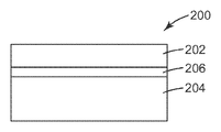
도 2는 제공된 방법에서 유용한 예시적인 반도체 구성의 개략 측면도이다.
<도 3>
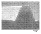
도 3은 실시예 1에서 생성된 식각된 반도체의 주사 전자 현미경사진이다.
<도 4a>
도 4a는 실시예 2에서 생성된 식각된 반도체의 주사 전자 현미경사진이다.
<도 4b>
도 4b는 실시예 2에서 생성된 식각된 반도체의 암시야 광학 현미경사진이다.
<도 5a>
도 5a는 실시예 3에 사용된 포토레지스트 패턴의 주사 전자 현미경사진이다.
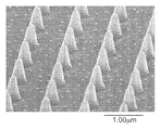
<도 5b 및 도 5c>
도 5b 및 도 5c는 실시예 3에서 생성된 식각된 반도체의 주사 전자 현미경사진이다.1A to 1B.
1A-1B are schematic side views of the steps of a provided method.
2,
2 is a schematic side view of an exemplary semiconductor configuration useful in the provided method.
3,
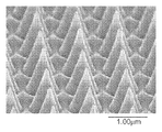
3 is a scanning electron micrograph of the etched semiconductor produced in Example 1. FIG.
4A,
4A is a scanning electron micrograph of the etched semiconductor produced in Example 2. FIG.
4 (b)
4B is a dark field optical micrograph of the etched semiconductor produced in Example 2. FIG.
Figure 5a
5A is a scanning electron micrograph of the photoresist pattern used in Example 3. FIG.
5b and 5c
5B and 5C are scanning electron micrographs of etched semiconductors produced in Example 3. FIG.
하기의 설명에서, 명세서의 일부를 형성하며 몇몇 특정 실시 형태가 예로서 도시되어 있는 첨부 도면을 참조한다. 본 발명의 범주 또는 사상으로부터 벗어남이 없이 다른 실시 형태가 고려되고 이루어질 수 있음을 이해하여야 한다. 따라서, 하기의 상세한 설명은 제한적인 의미로 취해져서는 안 된다.In the following description, reference is made to the accompanying drawings, which form a part of the specification and in which some specific embodiments are shown by way of example. It is to be understood that other embodiments may be contemplated and made without departing from the scope or spirit of the invention. Accordingly, the following detailed description should not be taken in a limiting sense.
달리 표시되지 않는 한, 본 명세서 및 특허청구범위에 사용되는 특징부의 크기, 양 및 물리적 특성을 표현하는 모든 숫자는 모든 경우에 "약"이라는 용어로 수식되는 것으로 이해되어야 한다. 따라서, 반대로 표시되지 않는 한, 전술한 명세서 및 첨부된 특허청구범위에 기재된 수치적 파라미터는 당업자가 본 명세서에 개시된 교시를 이용하여 얻고자 하는 원하는 특성에 따라 변할 수 있는 근사치이다. 종점(end point)에 의한 수치 범위의 사용은 그 범위 내의 모든 수 (예를 들어, 1 내지 5는 1, 1.5, 2, 2.75, 3, 3.80, 4 및 5를 포함함) 및 그 범위 내의 임의의 범위를 포함한다.Unless otherwise indicated, all numbers expressing the size, quantity, and physical properties of features used in this specification and claims are to be understood as being modified in all instances by the term "about." Thus, unless indicated to the contrary, the numerical parameters set forth in the foregoing specification and the appended claims are approximations that may vary depending upon the desired properties sought by those skilled in the art using the teachings disclosed herein. The use of a numerical range by end point can be any number within that range (e.g., 1 to 5 includes 1, 1.5, 2, 2.75, 3, 3.80, 4, and 5) and any within that range. Coverage of
제공된 방법은 종래의 식각 장비를 이용할 수 있으며, 따라서 특수 장비의 필요성을 제거할 수 있다. 제공된 방법은 반응성-이온 식각 대신 스퍼터 식각을 이용하며, 따라서 반응성-이온과 반응성이 아닌 반도체, 예를 들어, 비규소 재료로 제조된 반도체에서 유용하다. 일부 실시 형태에서, 이들 반도체는, 예를 들어 III-V 반도체, 예를 들어, GaAs, InP, AlGaAs, GaInAsP, 또는 GaInNAs를 포함한다. 다른 실시 형태에서, 제공된 방법은, 예를 들어 카드뮴, 마그네슘, 아연, 황, 셀레늄, 텔루륨, 및 그들의 조합을 포함할 수 있는 재료와 같은 II-VI 반도체를 식각하기에 유용하다. 예시적인 II-VI 반도체 재료는 CdMgZnSe 합금을 포함할 수 있다. CdZnSe, ZnSSe, ZnMgSSe,ZnS, CdS, ZnSe, ZnTe, ZnSeTe, HgCdSe, 및 HgCdTe와 같은 다른 II-VI 반도체가 또한 제공된 방법을 이용하여 식각될 수 있다.The provided method can utilize conventional etching equipment, thus eliminating the need for special equipment. The provided method utilizes sputter etching instead of reactive-ion etching and is therefore useful in semiconductors that are not reactive with reactive-ions, such as semiconductors made from non-silicon materials. In some embodiments, these semiconductors include, for example, III-V semiconductors, such as GaAs, InP, AlGaAs, GaInAsP, or GaInNAs. In other embodiments, provided methods are useful for etching II-VI semiconductors, such as materials that may include, for example, cadmium, magnesium, zinc, sulfur, selenium, tellurium, and combinations thereof. Exemplary II-VI semiconductor materials may include CdMgZnSe alloys. Other II-VI semiconductors such as CdZnSe, ZnSSe, ZnMgSSe, ZnS, CdS, ZnSe, ZnTe, ZnSeTe, HgCdSe, and HgCdTe can also be etched using the provided methods.
제공된 방법은 반도체의 스퍼터 식각 방법에 관한 것이다. 식각에 저항하여 식각되는 반도체 표면의 일부를 한정하는 식각 마스크가 위에 있는 반도체가 제공된다. 전형적인 식각 마스크는 경질 재료, 예를 들어, SiO2, Si3N4, 및 티타늄 또는 텅스텐과 같은 금속으로 제조될 수 있다. 그러나, 이들 경질 재료로 제조된 마스크는 제작하는 데 다소 시간이 걸리며(그가 침착된 후 포토레지스트를 이용하여 패턴화되어야 하기 때문임) 마스크는 때로는 반도체의 식각 속도와 유사한 속도로 스퍼터 식각에 의해 식각될 수 있다. 포토레지스트만이 식각 마스크로서 또한 유용할 수 있다. 포토레지스트 식각 마스크는 방사선에 노출시 염기성 현상제에 가용성이 되는 중합체로 이루어진 포지티브 포토레지스트 및 방사선에 노출시 가교결합하여 불용성이 되는 네거티브 포토레지스트를 포함할 수 있다. 예시적인 포지티브 포토레지스트는 UV5 포토레지스트 및 쉽리(Shipley) 1813 포토레지스트(둘 모두 미국 매사추세츠주 말보로 소재의 롬 앤드 하스 일렉트로닉 머티리얼스(Rohm and Hass Electronic Materials)로부터 입수가능함)를 포함한다. 예시적인 네거티브 포토레지스트는 UVN 30(롬 앤드 하스 일렉트로닉 머티리얼스로부터 입수가능함), 및 퓨쳐렉스(FUTURREX) 네거티브 포토레지스트, 예를 들어 NR9-1000P 및 NR9-3000PY(미국 뉴저지주 프랭클린 소재의 퓨쳐렉스로부터 입수가능함)을 포함한다. 포토레지스트는 반도체 리소그래피 분야의 당업자에게 잘 알려져 있다. 포토레지스트 식각 마스크를 이용하여 II-VI 또는 III-V 반도체를 스퍼터 식각하는 방법은 본 출원과 동일자에 출원된 공계류중인 출원, 대리인 문서 번호 제65811US002호에 설명되어 있다.The provided method relates to a sputter etching method of a semiconductor. A semiconductor is provided with an etch mask overlying a portion of the semiconductor surface that is etched in response to etching. Typical etching masks can be made of hard materials, such as SiO 2 , Si 3 N 4 , and metals such as titanium or tungsten. However, masks made from these hard materials take some time to fabricate (because they must be patterned using photoresist after they are deposited) and masks are sometimes etched by sputter etching at a rate similar to that of semiconductors. Can be. Only photoresist may also be useful as an etch mask. The photoresist etch mask may comprise a positive photoresist made of a polymer that is soluble in a basic developer upon exposure to radiation and a negative photoresist that becomes insoluble by crosslinking upon exposure to radiation. Exemplary positive photoresists include UV5 photoresists and Shipley 1813 photoresists (both available from Rohm and Hass Electronic Materials, Marlborough, Mass.). Exemplary negative photoresists are UVN 30 (available from Rohm and Haas Electronic Materials), and Futurex negative photoresists, such as NR9-1000P and NR9-3000PY (Furtex, Franklin, NJ). Available). Photoresists are well known to those skilled in the art of semiconductor lithography. A method of sputter etching II-VI or III-V semiconductors using photoresist etching masks is described in co-pending application, agent document no.
반도체 재료는 비반응성 식각 가스의 이온으로 반도체 표면에 충격을 가함으로써, 식각 마스크에 의해 차단되지 않은 영역에서 스퍼터 식각될 수 있다. 식각 가스 이온은 반도체의 노출된 표면으로부터 재료(부산물)를 제거하거나 방출시킬 수 있다. 식각은 전형적으로 식각 마스크에 의해 보호되지 않은 반도체 표면 상에서 발생한다. 식각 마스크는, 예를 들어 이미지 픽셀을 한정하거나 반도체 재료의 표면 상에 광 추출기를 생성하기 위한 패턴을 제공하는 패턴화된 개구를 가질 수 있다. 비반응성 식각 가스 이온은 사실상 수직 방식으로 반도체 재료의 표면 상에 충돌할 수 있다. 즉, 식각제 이온은 본질적으로 직선으로 - 전형적으로 반도체 재료의 표면에 직각 또는 거의 직각으로 - 반도체 재료의 표면을 타격하도록 구성될 수 있다. 식각제는 운동 에너지의 전달에 의해 반도체 재료로부터 노출된 분자를 제거하거나 방출할 수 있다.The semiconductor material can be sputter etched in an area not blocked by the etch mask by impacting the semiconductor surface with ions of the non-reactive etching gas. Etch gas ions may remove or release the material (by-products) from the exposed surface of the semiconductor. Etching typically occurs on a semiconductor surface that is not protected by an etch mask. The etching mask may have a patterned opening that defines a pattern for defining an image pixel or for generating a light extractor on the surface of the semiconductor material, for example. Non-reactive etching gas ions can impinge on the surface of the semiconductor material in a substantially vertical manner. That is, the etchant ions may be configured to strike the surface of the semiconductor material in an essentially straight line—typically at or near or perpendicular to the surface of the semiconductor material. The etchant can remove or release the exposed molecules from the semiconductor material by the transfer of kinetic energy.
예시적인 비반응성 식각 가스(식각제)는 아르곤, 크립톤, 크세논, 질소, 또는 그들의 조합을 포함할 수 있다. 이들 가스는 실질적으로 불활성 가스이므로 반도체 재료와 반응하는 경향이 거의 또는 전혀 없다. 따라서, 그들은 물리적 충격에 의해, 반도체 재료의 노출된 표면 상의 분자에 운동량을 전달함으로써 식각하는 경향을 갖는다. 이러한 재료는 그 후 방출될 수 있으며 반도체 벽의 식각된 수직 표면과 같은 이전에 식각된 다른 표면 상에 침착될 수 있다. 대안적으로, 방출된 재료는 파편으로서 진공 챔버 내의 어딘가에 침착될 수 있다. 파편은 축적되어 결국에는 식각 공정을 오염시킬 수 있다. 파편은 전형적으로 진공 챔버를 세정함으로써 주기적으로 제거된다.Exemplary non-reactive etching gases (etchants) may include argon, krypton, xenon, nitrogen, or combinations thereof. These gases are substantially inert gases and therefore have little or no tendency to react with semiconductor materials. Thus, they tend to etch by transferring physical momentum to molecules on the exposed surface of the semiconductor material. Such material may then be released and deposited on other previously etched surfaces, such as etched vertical surfaces of semiconductor walls. Alternatively, the released material may be deposited somewhere in the vacuum chamber as debris. Debris can accumulate and eventually contaminate the etching process. Debris is typically removed periodically by cleaning the vacuum chamber.
놀랍게도, 둘 모두가 예를 들어 아르곤과 같은 비반응성 가스를 이용하여 스퍼터 식각될 때, 포토레지스트로 제조된 식각 마스크가 II-VI 또는 III-V 반도체에 비하여 스퍼터 식각에 대해 높은 선택성을 가질 수 있음이 밝혀졌다. 예를 들어, 포토레지스트가 네거티브 포토레지스트, 예를 들어 NR9-1000P 또는 NR9-3000PY(미국 뉴저지주 프랭클린 소재의 퓨쳐렉스로부터 입수가능함)이고, 반도체가 II-VI 반도체, 예를 들어 CdMgZnSe일 경우, 반도체는 포토레지스트보다 6 내지 12배 빠른 속도로 식각되는 것으로 밝혀졌다. 제공된 방법의 일부 실시 형태에서, 반도체는 약 100 ㎚/min 초과, 약 300 ㎚/min 초과, 약 500 ㎚/min 초과, 또는 심지어 약 1000 ㎚/min 초과의 속도로 식각될 수 있다. 일부 실시 형태에서, 포토레지스트 식각 마스크는 약 100 ㎚/min 미만, 약 50 ㎚/min 미만, 또는 심지어 약 25 ㎚/min 미만의 속도로 식각될 수 있다. 일부 실시 형태에서, 반도체 식각 속도 대 포토레지스트 식각 속도의 비는 약 3 초과, 약 6 초과, 약 10 초과, 또는 심지어 약 12 초과이다.Surprisingly, when both are sputter etched using a non-reactive gas such as, for example, argon, an etch mask made of photoresist may have a high selectivity for sputter etching over II-VI or III-V semiconductors. Turned out. For example, if the photoresist is a negative photoresist, such as NR9-1000P or NR9-3000PY (available from Futurex, Franklin, NJ), and the semiconductor is a II-VI semiconductor, such as CdMgZnSe, The semiconductor has been found to be etched 6-12 times faster than photoresist. In some embodiments of provided methods, the semiconductor may be etched at a rate of greater than about 100 nm / min, greater than about 300 nm / min, greater than about 500 nm / min, or even greater than about 1000 nm / min. In some embodiments, the photoresist etch mask may be etched at a rate of less than about 100 nm / min, less than about 50 nm / min, or even less than about 25 nm / min. In some embodiments, the ratio of semiconductor etch rate to photoresist etch rate is greater than about 3, greater than about 6, greater than about 10, or even greater than about 12.
제공된 방법은 도면을 참조하여 더 잘 이해될 수 있다. 도 1a 내지 도 1b는 제공된 방법의 단계의 개략 측면도이다. 도 1a는 패턴화된 포토레지스트(104)가 위에 배치된 반도체 재료(102)를 포함하는 도면이다. 패턴화된 포토레지스트(104)는 반도체 재료(102)의 일부를 노출시키는 트렌치(103)를 갖는다. 반도체 재료(102)의 스퍼터 식각은 비반응성 가스를 이용하여 수행된다. 도 1b는 스퍼터 식각 후, 트렌치(103)가 확대되어 포토레지스트(104)에 의해 덮이지 않은 노출된 반도체 재료(102)의 일부가 반도체 재료(102)의 원래 표면 아래에서 식각되었음을 도시한다.The provided method can be better understood with reference to the drawings. 1A-1B are schematic side views of the steps of a provided method. 1A is a diagram that includes a
반도체의 제공된 이방성 식각 방법을 이용하여, 예를 들어 광 추출 요소와 같은 식각된 특징부를 반도체 내에 형성할 수 있다. 일부 실시 형태에서, 제공된 방법은 II-VI 반도체를 이용하여 제조된 전자장치 디바이스 상의 디스플레이에서 작은 픽셀을 한정하는 추출 요소를 식각하는 데 이용될 수 있다. 이들 픽셀은 매우 작을 수 있다. 예를 들어, 픽셀은 약 10 마이크로미터 미만의 최장 치수를 가질 수 있다. 픽셀은 약 1 마이크로미터인 트렌치에 의해 분리될 수 있다. 그러한 예시적인 디바이스는 하향-변환(down-converted) 발광 다이오드 (LED)를 포함한다. 다른 실시 형태에서, 제공된 방법은 II-VI 반도체로부터 제조된 LED의 면 상에 광 추출기를 형성하기 위해 이용될 수 있다. 그러한 광 추출기는 LED 면으로부터 방출되는 광의 양을 증가시킬 수 있다. 예시적인 광 추출 요소는 임의의 유형의 구조물로 제한되지 않는다. 일부 실시 형태에서, 광 추출 요소는, 예를 들어 미국 특허 출원 공개 제2009/0015757호(포츠(Potts) 등)에 개시된 바와 같은 회절 또는 산란 나노구조물; 예를 들어, 미국 특허 제6,347,874호와 제6,379,016호(둘 모두 보이드(Boyd) 등)에 개시된 바와 같은 라이저(riser)를 가진 구조물; 및 국제 특허 출원 공개 WO 2008/083188호(루(Lu) 등)에 개시된 것과 같은 구조물을 포함할 수 있다. 일부 실시 형태에서, 광 추출 요소는 약 500 ㎚만큼 작은 치수를 가질 수 있다.The provided anisotropic etching method of the semiconductor can be used to form etched features in the semiconductor, such as, for example, light extraction elements. In some embodiments, provided methods can be used to etch extraction elements that define small pixels in a display on an electronic device fabricated using II-VI semiconductors. These pixels can be very small. For example, a pixel can have a longest dimension of less than about 10 micrometers. The pixels may be separated by trenches that are about 1 micrometer in length. Such exemplary devices include down-converted light emitting diodes (LEDs). In other embodiments, provided methods can be used to form light extractors on the side of LEDs made from II-VI semiconductors. Such light extractors can increase the amount of light emitted from the LED side. Exemplary light extraction elements are not limited to any type of structure. In some embodiments, the light extracting elements may include diffraction or scattering nanostructures as disclosed, for example, in US Patent Application Publication No. 2009/0015757 (Potts et al.); Structures having risers as disclosed, for example, in US Pat. Nos. 6,347,874 and 6,379,016 (boyd, et al.); And structures such as those disclosed in WO 2008/083188 (Lu et al.). In some embodiments, the light extraction element can have a dimension as small as about 500 nm.
전형적으로, 아르곤 가스는 비반응성 식각 가스로 이용되는데, 이는, 예를 들어 염소 가스와 같은 반응성-이온 상호작용에 의해 식각하는 가스만큼 많이 반도체 특성을 열화시키지 않고 II-VI 또는 III-V 반도체를 효과적으로 식각하는 경향이 있기 때문이다. 그러나, 전술된 바와 같이, 원치않는 파편이 반도체의 스퍼터링에 의해 생성될 수 있다. 이들 파편은 플라즈마 식각 시스템의 내부 표면 상에 침착되어, 그에 따라서 시스템의 전기 특성을 변화시켜, 불안정한 식각 속도를 야기할 수 있다. 파편은 또한 잠재적으로 샘플 상에 재침착될 수 있다. 따라서, 비반응성 식각 가스를 이용할 경우, 진공 챔버로부터 반도체를 주기적으로 제거하고, 예를 들어, 염소, 산소, 또는 그들의 조합과 같은 반응성 가스로 챔버를 충전하여 진공 챔버 내부에 축적된 파편과 반응하여 이를 휘발시키도록 하는 것이 바람직하다. 매우 다양한 반응성 가스 및 반응성 가스의 조합이 챔버 세정에 사용될 수 있다. 이들은, 예를 들어 염소, 산소, 삼염화붕소, 사염화규소, 및 수소를 포함한다. 전형적으로 이들 반응성 가스는 아르곤, 헬륨, 또는 질소와 같은 비반응성 가스와 혼합될 수 있다.Typically, argon gas is used as a non-reactive etching gas, which does not deteriorate semiconductor properties as much as gas that is etched by reactive-ion interactions, such as chlorine gas, for example. This is because they tend to be etched effectively. However, as mentioned above, unwanted debris can be produced by sputtering of the semiconductor. These fragments may be deposited on the inner surface of the plasma etching system, thus changing the electrical properties of the system, resulting in unstable etching rates. Debris can also potentially be redeposited on the sample. Therefore, when using a non-reactive etching gas, the semiconductor is periodically removed from the vacuum chamber, and the chamber is filled with a reactive gas such as, for example, chlorine, oxygen, or a combination thereof to react with the debris accumulated inside the vacuum chamber. It is desirable to volatilize it. A wide variety of reactive gases and combinations of reactive gases can be used for chamber cleaning. These include, for example, chlorine, oxygen, boron trichloride, silicon tetrachloride, and hydrogen. Typically these reactive gases can be mixed with non-reactive gases such as argon, helium, or nitrogen.
반도체를 더 깊게 스퍼터 식각하는 것이 필요한 경우에, 샘플을 목표 깊이의 일부까지 스퍼터 식각하고, 챔버로부터 샘플을 제거하고, 챔버를 세정하고, 이어서 샘플을 추가 식각을 위해 챔버로 돌려보내는 것이 유리할 수 있다. 이러한 식각-및-세정 사이클을 반복하여 임의의 원하는 식각 깊이에 도달할 수 있다.If it is necessary to sputter etch the semiconductor deeper, it may be advantageous to sputter etch the sample to a portion of the target depth, remove the sample from the chamber, clean the chamber, and then return the sample to the chamber for further etching. . This etch-and-clean cycle can be repeated to reach any desired etch depth.
본 발명의 목적 및 이점은 하기의 실시예에 의해 추가로 예시되지만, 이들 실시예에 인용된 특정 물질 및 그 양 뿐만 아니라 기타 조건이나 상세 사항은 본 발명을 부당하게 제한하는 것으로 해석되어서는 안된다.The objects and advantages of the present invention are further illustrated by the following examples, but the specific materials and amounts recited in these examples as well as other conditions or details should not be construed as unduly limiting the present invention.
실시예Example
CdMgZnSe 합금에 기반한 II-VI 반도체 색상 변환기 층 구조물을 InP 기판 상에 분자 빔 에피택시(molecular beam epitaxy)에 의해 성장시켰다. 색상 변환기 층 구조물은 도 2에 개략적으로 도시되며, 층 두께와 조성은 다음의 표 I에 나타난다. 도 2는 상부 윈도우(202), 흡수기(204), 및 상부 윈도우(202)의 조성으로부터 흡수기(204)까지 점진적으로 변하는 점진적 조성 층(206)을 포함하는 색상 변환기 층(200)의 개략도이다. 흡수기 층(도시 안함)에는, 펌프 광이 흡수기 층 내에 흡수되고 긴 파장에서 광을 재방출할 때 발생되는 캐리어를 포획하는 양자 우물(quantum well)이 매립된다. 색상 변환기 구조물의 상세한 설명은, 예를 들어 미국 특허 제7,402,831호(밀러(Miller) 등)에서 찾을 수 있다.II-VI semiconductor color converter layer structures based on CdMgZnSe alloys were grown by molecular beam epitaxy on InP substrates. The color converter layer structure is shown schematically in FIG. 2 and the layer thicknesses and compositions are shown in Table I below. 2 is a schematic diagram of a
[표 I]TABLE I

비교예Comparative example 1 - One - IIII -- VIVI 반도체의 Semiconductor ClCl 22 반응성 이온 Reactive ions 식각Etching
네거티브 포토레지스트(NR1-1000P, 미국 뉴저지주 프랭클린 소재의 퓨쳐렉스로부터 입수가능함) 및 종래의 접촉 리소그래피를 이용하여 전술된 II-VI 반도체 구조물 상에 리지(ridge)의 포토레지스트 패턴을 생성하였다. 그 후, 다음 실시예에서 설명되는 바와 같이 식각을 위해 샘플을 작은 조각으로 벽개하였다. 식각은 상업적인 반응성 이온 시스템(RIE, 모델 플라즈마 랩(Model PLASMA LAB) 시스템 100, 영국 야턴 소재의 옥스포드 인스트루먼츠(Oxford Instruments)로부터 입수가능함)에서 실시하였다.Negative photoresist (NR1-1000P, available from Futurex, Franklin, NJ) and conventional contact lithography were used to create ridge photoresist patterns on the aforementioned II-VI semiconductor structures. The sample was then cleaved into small pieces for etching as described in the next example. Etching was performed in a commercial reactive ion system (RIE, Model PLASMA LAB System 100, available from Oxford Instruments, Yaton, UK).
포토레지스트 마스크가 위에 있는 II-VI 반도체의 작은 벽개된 샘플을 Si 캐리어 웨이퍼 상에 놓고, RIE 챔버 내에 두고, 0.8 Pa(6 mTorr)의 압력과 4 × 30 초 간격의 식각 시간으로, 80 sccm Cl2, 5 sccm Ar, 75 내지 200 와트 무선 주파수(RF) 출력, 1200 와트 유도 결합 플라즈마 출력을 이용하여 플라즈마 식각하였다. 포토레지스트는 Cl2 플라즈마 식각에 의해 심각하게 손상되었다. 포토레지스트의 식각 속도는 1000 ㎚/min으로 측정되었다. 반도체의 식각 속도 대 포토레지스트의 속도의 비는 0.19였다. 따라서, 염소에 의해 생성된 반응성 화학종은 포토레지스트와 반응하며 그것이 II-VI 반도체를 식각하는 것보다 훨씬 빠르게 포토레지스트를 식각한다.A small cleaved sample of II-VI semiconductor with a photoresist mask on it is placed on a Si carrier wafer, placed in a RIE chamber, at a pressure of 0.8 Pa (6 mTorr) and etch time at intervals of 4 x 30 seconds, 80 sccm Cl Plasma etching was performed using 2 , 5 sccm Ar, 75-200 watt radio frequency (RF) output, 1200 watt inductively coupled plasma output. The photoresist was severely damaged by Cl 2 plasma etching. The etching rate of the photoresist was measured at 1000 nm / min. The ratio of the etch rate of the semiconductor to the rate of the photoresist was 0.19. Thus, reactive species produced by chlorine react with the photoresist and etch the photoresist much faster than it etches II-VI semiconductors.
실시예 1 - 포토레지스트 마스크를 가진 II-VI 반도체의 Ar 식각Example 1 Ar Etching of II-VI Semiconductor with Photoresist Mask
전술된 II-VI 반도체 색상 변환기 샘플을 미국 뉴저지주 프랭클린 소재의 퓨처렉스로부터 입수가능한 NR9-1000P 네거티브 포토레지스트를 이용하여 스트라이프 패턴을 가진 포토레지스트 마스크로 오버코팅하였다. 스트라이프 패턴은 치수가 2 ㎛ 와 100 ㎛였다. 포토레지스트 마스크가 위에 있는 II-VI 반도체의 작은 벽개된 샘플을 Si 캐리어 웨이퍼 상에 놓고, RIE 챔버 내에 두고, 0.5 내지 4.0 Pa(4 내지 30 mTorr)의 압력과 5 × 60 초 간격의 식각 시간으로, 5 내지 50 sccm Ar, 20 내지 200 와트 Rf 출력, 700 내지 2000 와트 유도 결합 플라즈마 출력(ICP)을 이용하여 플라즈마 식각하였다. 폭이 2 ㎛만큼 작은 픽셀 스트라이프는 처리 후 수 개월 동안 강한 광발광(photoluminescence)을 계속 보여주었다. 식각 시간이 6 × 30초 간격(이 간격 동안 기판의 냉각을 허용하기 위함)인 것을 제외하고는 비교예 1에서와 동일한 조건하에서 Cl2로 식각한 동일 샘플은 1일 후에 광발광의 빠른 분해를 나타냈다. 도 3은 아르곤 스퍼터 식각 방법을 이용하여 식각된 반도체의 현미경사진이다. 얻어진 식각 프로파일은 약 63도의 벽 각도를 가졌다. 반도체 대 포토레지스트의 식각 속도의 비는 약 6 내지 약 12로 변하였으며 RF 출력을 변화시켜 제어할 수 있었다. 낮은 RF 출력은 상기 비를 증가시켰으나 식각 속도를 감소시켰다. II-VI 반도체 색상 변환기의 식각 속도는 300 ㎚/min 내지 500 ㎚/min 범위였다.The II-VI semiconductor color converter sample described above was overcoated with a photoresist mask with a stripe pattern using the NR9-1000P negative photoresist available from Futureex, Franklin, NJ. Stripe patterns had dimensions of 2 μm and 100 μm. A small cleaved sample of II-VI semiconductor with a photoresist mask on it is placed on a Si carrier wafer, placed in a RIE chamber, with a pressure of 0.5 to 4.0 Pa (4 to 30 mTorr) and an etch time of 5 x 60 seconds. Plasma etching was performed using 5 to 50 sccm Ar, 20 to 200 Watt Rf output, 700 to 2000 Watt Inductively Coupled Plasma Output (ICP). Pixel stripes as small as 2 μm continued to show strong photoluminescence for several months after treatment. The same sample etched with Cl 2 under the same conditions as in Comparative Example 1, except that the etching time was at 6 × 30 second intervals (to allow cooling of the substrate during this interval), resulted in rapid decomposition of photoluminescence after one day. Indicated. 3 is a micrograph of a semiconductor etched using an argon sputter etching method. The etch profile obtained had a wall angle of about 63 degrees. The ratio of etch rate of semiconductor to photoresist varied from about 6 to about 12 and could be controlled by varying the RF output. Low RF power increased the ratio but decreased the etching rate. The etching rate of the II-VI semiconductor color converter ranged from 300 nm / min to 500 nm / min.
실시예Example 2 - 2 - IIII -- VIVI 반도체 재료에서 3 마이크로미터 3 micrometers in semiconductor materials 트렌치의Trench ArAr 식각Etching
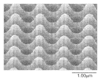
NR9-3000PY 네거티브 포토레지스트(미국 뉴저지주 프랭클린 소재의 퓨처렉스로부터 입수가능함)를 이용한 광학 리소그래피에 의해 제조된 표 1에서 전술된 바와 같은 II-VI 반도체 색상 변환기 구조물 상의 패턴화된 포토레지스트를 실시예 1의 절차를 이용하여 식각하였다. 도 4a는 생성된 구조물의 주사 전자 현미경사진이며 가로질러 대략 6 ㎛의 리지를 남기는 3 ㎛ 폭의 트렌치의 패턴을 도시한다. 도 4b는 반도체 리지의 광발광을 보여주는 암시야 광학 현미경사진이다. 관찰된 것은 일련의 방출 "픽셀"인데, 여기서 반도체 색상 변화기는 그대로 남아 있었다(포토레지스트에 의해 식각 동안 보호됨).Example a patterned photoresist on an II-VI semiconductor color converter structure as described above in Table 1 prepared by optical lithography using NR9-3000PY negative photoresist (available from Futurex, Franklin, NJ). It was etched using the procedure of 1. 4A is a scanning electron micrograph of the resulting structure and shows a pattern of 3 μm wide trenches leaving approximately 6 μm ridges across. 4B is a dark field optical micrograph showing photoluminescence of semiconductor ridges. What was observed was a series of emission "pixels" where the semiconductor color changer remained intact (protected during etching by the photoresist).
실시예 3 - 광 추출을 위한 II-VI 반도체의 Ar 플라즈마 식각Example 3 Ar Plasma Etching of II-VI Semiconductor for Light Extraction
표 1에서 전술된 바와 같은 II-VI 반도체 색상 변환기 구조물 상의 패턴화된 포토레지스트를 다음과 같이 제조하였다. 광 추출을 위해 구멍 또는 기둥 구조물을 가진 2-차원 격자 패턴을, 레이저 다이오드 공급원에 기초한 간섭 리소그래피를 이용하여 TELR-P003PM 포토레지스트(미국 매사추세츠주 말보로 소재의 쉽리로부터 입수가능함)에서 생성하였다. 격자는 1 ㎛ 피치로 400 내지 500 ㎚ 특징부를 가졌다. 패턴화된 포토레지스트-코팅된 반도체를 실시예 1에서 설명된 것과 유사한 조건하에서 Ar 식각되게 하였다. 도 5a는 식각 전에 반도체 상에 직경 400 ㎚의 기둥 구조물을 가진 포토레지스트 패턴의 주사 전자 현미경사진이다. 도 5b는 Ar 플라즈마 식각 후 도 5a와 동일한 도면을 도시하는데, 포토레지스트는 여전히 제자리에 있다. 식각 후, 남아 있는 포토레지스트는 구조가 피라미드형이었으며 포토레지스트 주변의 반도체는 식각되어 레지스트 아래에 원뿔 기둥을 남겼다(잔여 포토레지스트와 반도체 사이의 경계는 도 5b에서 볼 수 있으며, 기부에서 원뿔 구조의 꼭지점까지의 길이의 대략 2/3임). 추가의 Ar 식각은 도 5c에 도시된 반도체에서 패턴을 생성하였다. 광발광 측정은 도 5c에 예시된 식각된 샘플에 대해 50.4%의 외부 양자 효율을 나타냈다. 식각 전 평면 샘플의 광발광 측정은 29.7%의 외부 양자 효율을 나타냈다. 이러한 실시예는 II-VI 반도체 상의 광 추출 구조물이 방출되는 광의 수율을 어떻게 증가시키는지를 보여준다.The patterned photoresist on the II-VI semiconductor color converter structure as described above in Table 1 was prepared as follows. Two-dimensional grating patterns with hole or columnar structures for light extraction were generated in TELR-P003PM photoresist (available from Easily, Marlborough, Mass.) Using interference lithography based on laser diode sources. The grating had 400-500 nm features at a 1 μm pitch. The patterned photoresist-coated semiconductor was allowed to etch Ar under conditions similar to those described in Example 1. 5A is a scanning electron micrograph of a photoresist pattern with a pillar structure of 400 nm in diameter on a semiconductor prior to etching. 5B shows the same view as FIG. 5A after an Ar plasma etch, with the photoresist still in place. After etching, the remaining photoresist was pyramidal in structure and the semiconductor around the photoresist was etched away leaving a conical pillar under the resist (the boundary between the remaining photoresist and the semiconductor can be seen in FIG. Approximately two thirds of the length to the vertex). Further Ar etching produced a pattern in the semiconductor shown in FIG. 5C. Photoluminescence measurements showed an external quantum efficiency of 50.4% for the etched sample illustrated in FIG. 5C. Photoluminescence measurements of the preetched planar samples showed an external quantum efficiency of 29.7%. This example shows how the light extraction structure on the II-VI semiconductor increases the yield of light emitted.
본 발명의 범위 및 취지를 벗어나지 않고도 본 발명의 다양한 변형 및 변경이 당업자에게 명백하게 될 것이다. 본 발명은 본 명세서에 설명된 예시적인 실시 형태 및 실시예에 의해 부당하게 제한되는 것으로 의도되지 않고 그러한 실시예 및 실시 형태는 단지 예로서 제시된 것이며, 본 발명의 범주는 본 명세서에 하기와 같이 설명되는 특허청구범위에 의해서만 한정되는 것으로 의도됨을 이해하여야 한다. 본 개시 내용에 인용된 모든 참고 문헌은 전체적으로 본 명세서에 참고로 포함된다.Various modifications and alterations of this invention will become apparent to those skilled in the art without departing from the scope and spirit of this invention. The invention is not intended to be unduly limited by the illustrative embodiments and examples described herein and such examples and embodiments are presented by way of example only, and the scope of the invention is described herein as follows. It is to be understood that it is intended to be limited only by the claims that follow. All references cited in this disclosure are incorporated herein by reference in their entirety.
Claims (16)
반도체의 표면으로부터 재료를 제거하고 적어도 하나의 식각된 표면을 제공하기 위해 비반응성 식각 가스를 이용하여 식각 마스크를 통해 반도체를 스퍼터 식각하는 단계;
진공 챔버로부터 적어도 하나의 식각된 표면을 가진 반도체를 제거하는 단계; 및
진공 챔버를 세정하는 단계를 포함하며,
여기서 반도체는 III-V 반도체, II-VI 반도체, 또는 그들의 조합을 포함하며,
진공 챔버를 세정하는 단계는 진공 챔버 내로 반응성 가스를 도입하고 반응성 가스를 가진 플라즈마를 형성하여 진공 챔버 내의 침착물을 휘발시키는 단계를 포함하는 반도체 식각 방법.Providing a semiconductor with an etch mask over it in a vacuum chamber; And
Sputter etching the semiconductor through an etch mask using a non-reactive etching gas to remove material from the surface of the semiconductor and provide at least one etched surface;
Removing the semiconductor with at least one etched surface from the vacuum chamber; And
Cleaning the vacuum chamber,
Wherein the semiconductor comprises a III-V semiconductor, a II-VI semiconductor, or a combination thereof,
Cleaning the vacuum chamber includes introducing a reactive gas into the vacuum chamber and forming a plasma with the reactive gas to volatilize deposits in the vacuum chamber.
적어도 하나의 식각된 표면을 가진 반도체를 챔버 세정 후 진공 챔버로 돌려보내는 단계; 및
비반응성 식각 가스를 이용하여 식각 마스크를 통해 반도체를 추가로 스퍼터 식각하는 단계를 추가로 포함하는 방법.The method of claim 1,
Returning the semiconductor with at least one etched surface to the vacuum chamber after chamber cleaning; And
Further sputter etching the semiconductor through the etch mask using a non-reactive etching gas.
Applications Claiming Priority (2)
| Application Number | Priority Date | Filing Date | Title |
|---|---|---|---|
| US25929909P | 2009-11-09 | 2009-11-09 | |
| US61/259,299 | 2009-11-09 |
Publications (1)
| Publication Number | Publication Date |
|---|---|
| KR20120095411A true KR20120095411A (en) | 2012-08-28 |
Family
ID=43970710
Family Applications (1)
| Application Number | Title | Priority Date | Filing Date |
|---|---|---|---|
| KR1020127014823A KR20120095411A (en) | 2009-11-09 | 2010-11-02 | Etching process for semiconductors |
Country Status (7)
| Country | Link |
|---|---|
| US (1) | US8765611B2 (en) |
| EP (1) | EP2499663A2 (en) |
| JP (1) | JP5723377B2 (en) |
| KR (1) | KR20120095411A (en) |
| CN (1) | CN102893378A (en) |
| TW (1) | TW201135832A (en) |
| WO (1) | WO2011056783A2 (en) |
Families Citing this family (12)
| Publication number | Priority date | Publication date | Assignee | Title |
|---|---|---|---|---|
| JP5710433B2 (en) * | 2011-09-13 | 2015-04-30 | 株式会社東芝 | Film forming apparatus cleaning method and film forming apparatus |
| FR2984769B1 (en) * | 2011-12-22 | 2014-03-07 | Total Sa | METHOD FOR TEXTURING THE SURFACE OF A SILICON SUBSTRATE, STRUCTURED SUBSTRATE, AND PHOTOVOLTAIC DEVICE COMPRISING SUCH A STRUCTURED SUBSTRATE |
| US8883028B2 (en) | 2011-12-28 | 2014-11-11 | Lam Research Corporation | Mixed mode pulsing etching in plasma processing systems |
| EP2922103B1 (en) | 2012-08-21 | 2017-04-05 | Oji Holdings Corporation | Substrate for semiconductor light emitting elements and semiconductor light emitting element |
| WO2014051909A1 (en) * | 2012-09-25 | 2014-04-03 | Applied Materials, Inc. | Chamber clean with in gas heating source |
| CN103901516B (en) * | 2012-12-26 | 2016-06-15 | 清华大学 | The preparation method of grating |
| US8941145B2 (en) * | 2013-06-17 | 2015-01-27 | The Boeing Company | Systems and methods for dry etching a photodetector array |
| US9012305B1 (en) * | 2014-01-29 | 2015-04-21 | Applied Materials, Inc. | Wafer dicing using hybrid laser scribing and plasma etch approach with intermediate non-reactive post mask-opening clean |
| JP6871706B2 (en) | 2016-09-30 | 2021-05-12 | 日機装株式会社 | Manufacturing method of semiconductor light emitting device |
| JPWO2021095608A1 (en) * | 2019-11-12 | 2021-05-20 | ||
| CN113823992B (en) * | 2021-09-14 | 2022-11-11 | 苏州长瑞光电有限公司 | Semiconductor device manufacturing method and semiconductor device |
| CN115343788B (en) * | 2022-08-18 | 2024-03-15 | 上海交通大学 | Quartz micro-lens preparation method based on cyclic etching process and quartz micro-lens |
Family Cites Families (23)
| Publication number | Priority date | Publication date | Assignee | Title |
|---|---|---|---|---|
| JPH0294522A (en) * | 1988-09-30 | 1990-04-05 | Toshiba Corp | Dry etching method |
| US5404027A (en) * | 1991-05-15 | 1995-04-04 | Minnesota Mining & Manufacturing Compay | Buried ridge II-VI laser diode |
| DE69320963T2 (en) * | 1992-06-22 | 1999-05-12 | Lam Res Corp | PLASMA CLEANING METHOD FOR REMOVING RESIDUES IN A PLASMA TREATMENT CHAMBER |
| DE4241045C1 (en) * | 1992-12-05 | 1994-05-26 | Bosch Gmbh Robert | Process for anisotropic etching of silicon |
| JPH07335620A (en) * | 1994-06-09 | 1995-12-22 | Sony Corp | Selective dry-etching method for ii-vi group compound semiconductor |
| EP0774772A1 (en) | 1995-11-17 | 1997-05-21 | Applied Materials, Inc. | Methods for physically etching silicon electrically conducting surfaces |
| DE19736370C2 (en) * | 1997-08-21 | 2001-12-06 | Bosch Gmbh Robert | Process for anisotropic etching of silicon |
| KR100269323B1 (en) * | 1998-01-16 | 2000-10-16 | 윤종용 | Method for etching platinum layer in semiconductor device |
| IT1301840B1 (en) * | 1998-06-30 | 2000-07-07 | Stmicroelettronica S R L | Enhancing selectivity between light-sensitive material film and layer to be subjected to etching in electronic semiconductor device fabrication processes, involves radiating wafer with ion beam |
| DE19919832A1 (en) * | 1999-04-30 | 2000-11-09 | Bosch Gmbh Robert | Process for anisotropic plasma etching of semiconductors |
| SE9903213D0 (en) * | 1999-06-21 | 1999-09-10 | Carl Fredrik Carlstroem | Dry etching process of compound semiconductor materials |
| US6352081B1 (en) * | 1999-07-09 | 2002-03-05 | Applied Materials, Inc. | Method of cleaning a semiconductor device processing chamber after a copper etch process |
| US6347874B1 (en) * | 2000-02-16 | 2002-02-19 | 3M Innovative Properties Company | Wedge light extractor with risers |
| JP3776824B2 (en) * | 2002-04-05 | 2006-05-17 | 株式会社東芝 | Semiconductor light emitting device and manufacturing method thereof |
| DE10247913A1 (en) * | 2002-10-14 | 2004-04-22 | Robert Bosch Gmbh | Process for the anisotropic etching of structures in a substrate arranged in an etching chamber used in semiconductor manufacture comprises using an etching gas and a passivating gas which is fed to the chamber in defined periods |
| US7238970B2 (en) * | 2003-10-30 | 2007-07-03 | Matsushita Electric Industrial Co., Ltd. | Semiconductor device and method for fabricating the same |
| JP2005353972A (en) | 2004-06-14 | 2005-12-22 | Canon Inc | Plasma processing method |
| US7402831B2 (en) * | 2004-12-09 | 2008-07-22 | 3M Innovative Properties Company | Adapting short-wavelength LED's for polychromatic, broadband, or “white” emission |
| US7575007B2 (en) * | 2006-08-23 | 2009-08-18 | Applied Materials, Inc. | Chamber recovery after opening barrier over copper |
| WO2008083188A2 (en) | 2006-12-29 | 2008-07-10 | 3M Innovative Properties Company | Led light source with converging extractor in an optical element |
| US8179034B2 (en) * | 2007-07-13 | 2012-05-15 | 3M Innovative Properties Company | Light extraction film for organic light emitting diode display and lighting devices |
| CN101472455A (en) | 2007-12-29 | 2009-07-01 | 3M创新有限公司 | Electromagnetic shielding liner and method for filling clearance of electromagnetic shielding system |
| CN102473817A (en) * | 2009-06-30 | 2012-05-23 | 3M创新有限公司 | Cadmium-free re-emitting semiconductor construction |
-
2010
- 2010-11-02 JP JP2012537938A patent/JP5723377B2/en not_active Expired - Fee Related
- 2010-11-02 US US12/917,826 patent/US8765611B2/en not_active Expired - Fee Related
- 2010-11-02 KR KR1020127014823A patent/KR20120095411A/en not_active Application Discontinuation
- 2010-11-02 WO PCT/US2010/055096 patent/WO2011056783A2/en active Application Filing
- 2010-11-02 EP EP10828972A patent/EP2499663A2/en not_active Withdrawn
- 2010-11-02 CN CN2010800506808A patent/CN102893378A/en active Pending
- 2010-11-08 TW TW099138381A patent/TW201135832A/en unknown
Also Published As
| Publication number | Publication date |
|---|---|
| JP5723377B2 (en) | 2015-05-27 |
| CN102893378A (en) | 2013-01-23 |
| TW201135832A (en) | 2011-10-16 |
| US20110108956A1 (en) | 2011-05-12 |
| US8765611B2 (en) | 2014-07-01 |
| WO2011056783A3 (en) | 2011-07-28 |
| WO2011056783A2 (en) | 2011-05-12 |
| EP2499663A2 (en) | 2012-09-19 |
| JP2013510442A (en) | 2013-03-21 |
Similar Documents
| Publication | Publication Date | Title |
|---|---|---|
| US8765611B2 (en) | Etching process for semiconductors | |
| US6762134B2 (en) | Metal-assisted chemical etch to produce porous group III-V materials | |
| US8273663B2 (en) | Process for anisotropic etching of semiconductors | |
| EP3026716B1 (en) | Semiconductor light emitting element and method for manufacturing same | |
| Park et al. | Enhancement of photo-and electro-luminescence of GaN-based LED structure grown on a nanometer-scaled patterned sapphire substrate | |
| KR20180061093A (en) | Method for forming nano patterns, method for preparing light emitting device and light emitting device prepared by the same | |
| US20130140596A1 (en) | Light emitting diode | |
| Park et al. | Low angle forward reflected neutral beam source and its applications | |
| KR20180060585A (en) | Method for forming nano patterns, method for preparing light emitting device and light emitting device prepared by the same | |
| Pearton et al. | Science of dry etching of III-V materials | |
| JP2017063099A (en) | Method for manufacturing substrate including uneven structure, and method for manufacturing semiconductor light-emitting device | |
| Byeon et al. | Enhancement of the photon extraction of green and blue LEDs by patterning the indium tin oxide top layer | |
| KR101586441B1 (en) | Method for etching of palladium layer for opto-electronic device | |
| Jaloustre et al. | Preferential crystal orientation etching of GaN nanopillars in Cl2 plasma | |
| CN112921403A (en) | Etching method of silicon carbide wafer | |
| Teo et al. | Deep reactive ion etching for pillar type nanophotonic crystal | |
| KR100780832B1 (en) | Dry etching method for zno materials | |
| Pearton et al. | Semiconductor (III-V) Thin Films: Plasma Etching | |
| Forchel et al. | InP/InGaAs nanofabrication and optical characterization | |
| Lee et al. | Emission Enhancement of InGaN/GaN Light Emitting Diode by Using Ag Nanoparticles | |
| Pearton | Dry Etching of Semiconductors at the Nano-and Micro-Scale | |
| Irrera et al. | Room Temperature Light Emission from Silicon Nanowires Fabricated by a Metal-Assisted Wet Etching Process | |
| Batoni et al. | Very Low Pressure Magnetron Reactive Ion Etching of GaN and Al x Ga 1− x N Using Dichlorofluoromethane (Halocarbon 12) | |
| EP1557874A2 (en) | Method for etching high aspect ratio features in III-V based compounds for optoelectronic devices | |
| Doan et al. | Enhanced cathodoluminescence of KOH-treated InGaN/GaN LEDs with deep nano-hole arrays |
Legal Events
| Date | Code | Title | Description |
|---|---|---|---|
| WITN | Application deemed withdrawn, e.g. because no request for examination was filed or no examination fee was paid |